364
Arria V Device Handbook Volume 1: Device Interfaces and Integration Subscribe Send Feedback AV-5V2 2019.10.03 101 Innovation Drive San Jose, CA 95134 www.altera.com
Arria V Device HandbookVolume 1: Device Interfaces and Integration
Subscribe
Send Feedback
AV-5V22019.10.03
101 Innovation DriveSan Jose, CA 95134www.altera.com
Contents
Logic Array Blocks and Adaptive Logic Modules in Arria V Devices............... 1-1LAB ............................................................................................................................................................... 1-1
MLAB ............................................................................................................................................... 1-2Local and Direct Link Interconnects ............................................................................................1-4LAB Control Signals........................................................................................................................ 1-5ALM Resources ............................................................................................................................... 1-7ALM Output .................................................................................................................................... 1-9
ALM Operating Modes ............................................................................................................................ 1-11Normal Mode ................................................................................................................................ 1-11Extended LUT Mode .................................................................................................................... 1-12Arithmetic Mode ...........................................................................................................................1-12Shared Arithmetic Mode ..............................................................................................................1-13
Logic Array Blocks and Adaptive Logic Modules in Arria V Devices Revision History................. 1-15
Embedded Memory Blocks in Arria V Devices.................................................. 2-1Types of Embedded Memory..................................................................................................................... 2-1
Embedded Memory Capacity in Arria V Devices.......................................................................2-2Embedded Memory Design Guidelines for Arria V Devices.................................................................2-2
Guideline: Consider the Memory Block Selection...................................................................... 2-2Guideline: Implement External Conflict Resolution...................................................................2-3Guideline: Customize Read-During-Write Behavior.................................................................. 2-3Guideline: Consider Power-Up State and Memory Initialization............................................. 2-7Guideline: Control Clocking to Reduce Power Consumption...................................................2-7
Embedded Memory Features..................................................................................................................... 2-7Embedded Memory Configurations..............................................................................................2-9Mixed-Width Port Configurations.............................................................................................. 2-10
Embedded Memory Modes...................................................................................................................... 2-12Embedded Memory Clocking Modes..................................................................................................... 2-14
Clocking Modes for Each Memory Mode.................................................................................. 2-14Asynchronous Clears in Clocking Modes.................................................................................. 2-15Output Read Data in Simultaneous Read/Write........................................................................2-15Independent Clock Enables in Clocking Modes........................................................................2-15
Parity Bit in Memory Blocks.....................................................................................................................2-15Byte Enable in Embedded Memory Blocks............................................................................................ 2-16
Byte Enable Controls in Memory Blocks.................................................................................... 2-16Data Byte Output........................................................................................................................... 2-16RAM Blocks Operations............................................................................................................... 2-17
Memory Blocks Packed Mode Support...................................................................................................2-17Memory Blocks Address Clock Enable Support.................................................................................... 2-17Memory Blocks Error Correction Code Support.................................................................................. 2-19
Error Correction Code Truth Table.............................................................................................2-19Embedded Memory Blocks in Arria V Devices Revision History...................................................... 2-20
TOC-2 Arria V Device Handbook Volume 1: Device Interfaces and Integration
Altera Corporation
Variable Precision DSP Blocks in Arria V Devices.............................................3-1Features..........................................................................................................................................................3-1Supported Operational Modes in Arria V Devices................................................................................. 3-2Resources.......................................................................................................................................................3-4Design Considerations................................................................................................................................ 3-5
Operational Modes.......................................................................................................................... 3-5Internal Coefficient and Pre-Adder............................................................................................... 3-6Accumulator..................................................................................................................................... 3-6Chainout Adder................................................................................................................................3-7
Block Architecture....................................................................................................................................... 3-7Input Register Bank....................................................................................................................... 3-11Pre-Adder........................................................................................................................................3-16Internal Coefficient........................................................................................................................ 3-17Multipliers....................................................................................................................................... 3-17Adder............................................................................................................................................... 3-17Accumulator and Chainout Adder.............................................................................................. 3-18Systolic Registers............................................................................................................................ 3-18Double Accumulation Register.................................................................................................... 3-19Output Register Bank.................................................................................................................... 3-19
Operational Mode Descriptions.............................................................................................................. 3-19Independent Multiplier Mode......................................................................................................3-19Independent Complex Multiplier Mode..................................................................................... 3-27Multiplier Adder Sum Mode........................................................................................................ 3-33Sum of Square Mode......................................................................................................................3-3718 x 18 Multiplication Summed with 36-Bit Input Mode.........................................................3-38Systolic FIR Mode.......................................................................................................................... 3-39
Variable Precision DSP Blocks in Arria V Devices Revision History.................................................3-43
Clock Networks and PLLs in Arria V Devices.................................................... 4-1Clock Networks............................................................................................................................................ 4-1
Clock Resources in Arria V Devices..............................................................................................4-1Types of Clock Networks................................................................................................................ 4-3Clock Sources Per Quadrant...........................................................................................................4-6Types of Clock Regions................................................................................................................... 4-7Clock Network Sources................................................................................................................... 4-8Clock Output Connections...........................................................................................................4-11Clock Control Block...................................................................................................................... 4-11Clock Power Down........................................................................................................................ 4-14Clock Enable Signals......................................................................................................................4-14
Arria V PLLs............................................................................................................................................... 4-16PLL Physical Counters in Arria V Devices.................................................................................4-17PLL Locations in Arria V Devices............................................................................................... 4-17PLL Migration Guidelines ........................................................................................................... 4-22Fractional PLL Architecture......................................................................................................... 4-23PLL Cascading................................................................................................................................4-23PLL External Clock I/O Pins........................................................................................................ 4-24
Arria V Device Handbook Volume 1: Device Interfaces and Integration TOC-3
Altera Corporation

PLL Control Signals....................................................................................................................... 4-25Clock Feedback Modes..................................................................................................................4-26Clock Multiplication and Division.............................................................................................. 4-32Programmable Phase Shift............................................................................................................4-33Programmable Duty Cycle............................................................................................................4-33Clock Switchover............................................................................................................................4-33PLL Reconfiguration and Dynamic Phase Shift........................................................................ 4-38
Clock Networks and PLLs in Arria V Devices Revision History........................................................ 4-38
I/O Features in Arria V Devices..........................................................................5-1I/O Resources Per Package for Arria V Devices...................................................................................... 5-1I/O Vertical Migration for Arria V Devices............................................................................................. 5-4
Verifying Pin Migration Compatibility.........................................................................................5-5I/O Standards Support in Arria V Devices...............................................................................................5-5
I/O Standards Support for FPGA I/O in Arria V Devices..........................................................5-6I/O Standards Support for HPS I/O in Arria V Devices.............................................................5-7I/O Standards Voltage Levels in Arria V Devices........................................................................ 5-8MultiVolt I/O Interface in Arria V Devices................................................................................5-10
I/O Design Guidelines for Arria V Devices............................................................................................5-11Mixing Voltage-Referenced and Non-Voltage-Referenced I/O Standards.............................5-11Guideline: Use the Same VCCPD for All I/O Banks in a Group................................................5-12Guideline: Ensure Compatible VCCIO and VCCPD Voltage in the Same Bank....................... 5-13Guideline: VREF Pin Restrictions................................................................................................. 5-13Guideline: Observe Device Absolute Maximum Rating for 3.3 V Interfacing...................... 5-13Guideline: Use PLL Integer Mode for LVDS Applications....................................................... 5-14Guideline: Pin Placement for General Purpose High-Speed Signals...................................... 5-14
I/O Banks Locations in Arria V Devices................................................................................................ 5-14I/O Banks Groups in Arria V Devices.................................................................................................... 5-17
Modular I/O Banks for Arria V GX Devices..............................................................................5-18Modular I/O Banks for Arria V GT Devices..............................................................................5-20Modular I/O Banks for Arria V GZ Devices..............................................................................5-21Modular I/O Banks for Arria V SX Devices...............................................................................5-22Modular I/O Banks for Arria V ST Devices............................................................................... 5-23
I/O Element Structure in Arria V Devices............................................................................................. 5-23I/O Buffer and Registers in Arria V Devices.............................................................................. 5-24
Programmable IOE Features in Arria V Devices.................................................................................. 5-26Programmable Current Strength................................................................................................. 5-28Programmable Output Slew Rate Control..................................................................................5-29Programmable IOE Delay.............................................................................................................5-30Programmable Output Buffer Delay........................................................................................... 5-30Programmable Pre-Emphasis.......................................................................................................5-31Programmable Differential Output Voltage............................................................................... 5-31Open-Drain Output.......................................................................................................................5-32Pull-up Resistor.............................................................................................................................. 5-33Bus-Hold Circuitry........................................................................................................................ 5-33
On-Chip I/O Termination in Arria V Devices...................................................................................... 5-33RS OCT without Calibration in Arria V Devices.......................................................................5-34RS OCT with Calibration in Arria V Devices............................................................................ 5-36
TOC-4 Arria V Device Handbook Volume 1: Device Interfaces and Integration
Altera Corporation
RT OCT with Calibration in Arria V Devices............................................................................5-38Dynamic OCT in Arria V Devices.............................................................................................. 5-40LVDS Input RD OCT in Arria V Devices................................................................................... 5-41OCT Calibration Block in Arria V Devices................................................................................5-42
External I/O Termination for Arria V Devices......................................................................................5-45Single-ended I/O Termination..................................................................................................... 5-46Differential I/O Termination........................................................................................................ 5-48
I/O Features in Arria V Devices Revision History................................................................................ 5-54
High-Speed Differential I/O Interfaces and DPA in Arria V Devices................6-1Dedicated High-Speed Circuitries in Arria V Devices........................................................................... 6-2
SERDES and DPA Bank Locations in Arria V Devices.............................................................. 6-2LVDS SERDES Circuitry.................................................................................................................6-4True LVDS Buffers in Arria V Devices..........................................................................................6-5Emulated LVDS Buffers in Arria V Devices.................................................................................6-7
High-Speed I/O Design Guidelines for Arria V Devices........................................................................6-7PLLs and Clocking for Arria V Devices........................................................................................6-7LVDS Interface with External PLL Mode..................................................................................... 6-8Pin Placement Guidelines for DPA and Non-DPA Differential Channels.............................6-13
Differential Transmitter in Arria V Devices...........................................................................................6-21Transmitter Blocks......................................................................................................................... 6-21Transmitter Clocking.....................................................................................................................6-22Serializer Bypass for DDR and SDR Operations....................................................................... 6-23Programmable Differential Output Voltage............................................................................... 6-23Programmable Pre-Emphasis.......................................................................................................6-24
Differential Receiver in Arria V Devices................................................................................................ 6-25Receiver Blocks in Arria V Devices............................................................................................. 6-26Receiver Modes in Arria V Devices.............................................................................................6-30Receiver Clocking for Arria V Devices....................................................................................... 6-32Differential I/O Termination for Arria V Devices.....................................................................6-33
Source-Synchronous Timing Budget.......................................................................................................6-34Differential Data Orientation....................................................................................................... 6-34Differential I/O Bit Position..........................................................................................................6-34Transmitter Channel-to-Channel Skew...................................................................................... 6-36Receiver Skew Margin for Non-DPA Mode............................................................................... 6-36
High-Speed Differential I/O Interfaces and DPA in Arria V Devices Revision History..................6-39
External Memory Interfaces in Arria V Devices.................................................7-1External Memory Performance..................................................................................................................7-2HPS External Memory Performance.........................................................................................................7-2Memory Interface Pin Support in Arria V Devices.................................................................................7-3
Guideline: Using DQ/DQS Pins.....................................................................................................7-3DQ/DQS Bus Mode Pins for Arria V Devices............................................................................. 7-4DQ/DQS Groups in Arria V GX....................................................................................................7-5DQ/DQS Groups in Arria V GT....................................................................................................7-7DQ/DQS Groups in Arria V GZ....................................................................................................7-8DQ/DQS Groups in Arria V SX.....................................................................................................7-8
Arria V Device Handbook Volume 1: Device Interfaces and Integration TOC-5
Altera Corporation
DQ/DQS Groups in Arria V ST.....................................................................................................7-9External Memory Interface Features in Arria V Devices..................................................................... 7-10
UniPHY IP...................................................................................................................................... 7-10External Memory Interface Datapath......................................................................................... 7-10DQS Phase-Shift Circuitry............................................................................................................7-12PHY Clock (PHYCLK) Networks................................................................................................7-20DQS Logic Block............................................................................................................................ 7-23Leveling Circuitry for Arria V GZ Devices................................................................................ 7-26Dynamic OCT Control................................................................................................................. 7-28IOE Registers.................................................................................................................................. 7-28Delay Chains...................................................................................................................................7-31I/O and DQS Configuration Blocks............................................................................................ 7-34
Hard Memory Controller..........................................................................................................................7-34Features of the Hard Memory Controller................................................................................... 7-35Multi-Port Front End ....................................................................................................................7-37Bonding Support............................................................................................................................ 7-37Hard Memory Controller Width for Arria V GX......................................................................7-41Hard Memory Controller Width for Arria V GT...................................................................... 7-41Hard Memory Controller Width for Arria V SX.......................................................................7-42Hard Memory Controller Width for Arria V ST....................................................................... 7-42
External Memory Interfaces in Arria V Devices Revision History.....................................................7-43
Configuration, Design Security, and Remote System Upgrades in Arria VDevices............................................................................................................. 8-1
Enhanced Configuration and Configuration via Protocol..................................................................... 8-1MSEL Pin Settings........................................................................................................................................8-2Configuration Sequence..............................................................................................................................8-4
Power Up........................................................................................................................................... 8-6Reset...................................................................................................................................................8-6Configuration................................................................................................................................... 8-7Configuration Error Handling....................................................................................................... 8-7Initialization......................................................................................................................................8-7User Mode......................................................................................................................................... 8-7
Configuration Timing Waveforms.............................................................................................................8-8FPP Configuration Timing............................................................................................................. 8-8AS Configuration Timing............................................................................................................. 8-10PS Configuration Timing..............................................................................................................8-11
Device Configuration Pins........................................................................................................................8-11I/O Standards and Drive Strength for Configuration Pins.......................................................8-14Configuration Pin Options in the Intel Quartus Prime Software............................................8-14
Fast Passive Parallel Configuration..........................................................................................................8-15Fast Passive Parallel Single-Device Configuration.................................................................... 8-15Fast Passive Parallel Multi-Device Configuration..................................................................... 8-16Transmitting Configuration Data................................................................................................ 8-18
Active Serial Configuration...................................................................................................................... 8-19DATA Clock (DCLK).................................................................................................................... 8-20Active Serial Single-Device Configuration................................................................................. 8-20Active Serial Multi-Device Configuration..................................................................................8-21
TOC-6 Arria V Device Handbook Volume 1: Device Interfaces and Integration
Altera Corporation
Estimating the Active Serial Configuration Time..................................................................... 8-23Using EPCS and EPCQ Devices...............................................................................................................8-23
Controlling EPCS and EPCQ Devices........................................................................................ 8-24Trace Length and Loading Guideline..........................................................................................8-24Programming EPCS and EPCQ Devices.................................................................................... 8-24
Passive Serial Configuration.....................................................................................................................8-28Passive Serial Single-Device Configuration Using an External Host......................................8-29Passive Serial Single-Device Configuration Using an Altera Download Cable.....................8-29Passive Serial Multi-Device Configuration.................................................................................8-30
JTAG Configuration.................................................................................................................................. 8-33JTAG Single-Device Configuration............................................................................................. 8-34JTAG Multi-Device Configuration.............................................................................................. 8-35CONFIG_IO JTAG Instruction................................................................................................... 8-36
Configuration Data Compression............................................................................................................8-37Enabling Compression Before Design Compilation................................................................. 8-37Enabling Compression After Design Compilation....................................................................8-37Using Compression in Multi-Device Configuration.................................................................8-37
Remote System Upgrades..........................................................................................................................8-38Configuration Images....................................................................................................................8-39Configuration Sequence in the Remote Update Mode............................................................. 8-40Remote System Upgrade Circuitry.............................................................................................. 8-40Enabling Remote System Upgrade Circuitry............................................................................. 8-41Remote System Upgrade Registers.............................................................................................. 8-42Remote System Upgrade State Machine..................................................................................... 8-43User Watchdog Timer................................................................................................................... 8-43
Design Security...........................................................................................................................................8-44Altera Unique Chip ID IP Core....................................................................................................8-45JTAG Secure Mode.........................................................................................................................8-45Security Key Types.........................................................................................................................8-45Security Modes............................................................................................................................... 8-46Design Security Implementation Steps....................................................................................... 8-47
Configuration, Design Security, and Remote System Upgrades in Arria V Devices RevisionHistory................................................................................................................................................... 8-47
SEU Mitigation for Arria V Devices................................................................... 9-1Error Detection Features.............................................................................................................................9-1Configuration Error Detection...................................................................................................................9-1User Mode Error Detection........................................................................................................................ 9-1Specifications................................................................................................................................................ 9-2
Minimum EMR Update Interval....................................................................................................9-2Error Detection Frequency............................................................................................................. 9-3CRC Calculation Time For Entire Device.................................................................................... 9-3
Using Error Detection Features in User Mode.........................................................................................9-4Enabling Error Detection................................................................................................................9-5CRC_ERROR Pin.............................................................................................................................9-5Error Detection Registers................................................................................................................9-5Error Detection Process.................................................................................................................. 9-8Testing the Error Detection Block................................................................................................. 9-9
Arria V Device Handbook Volume 1: Device Interfaces and Integration TOC-7
Altera Corporation
SEU Mitigation for Arria V Devices Revision History......................................................................... 9-10
JTAG Boundary-Scan Testing in Arria V Devices............................................ 10-1BST Operation Control ............................................................................................................................ 10-1
IDCODE .........................................................................................................................................10-1Supported JTAG Instruction ....................................................................................................... 10-3JTAG Secure Mode ........................................................................................................................10-7JTAG Private Instruction ............................................................................................................. 10-7
I/O Voltage for JTAG Operation .............................................................................................................10-8Performing BST .........................................................................................................................................10-8Enabling and Disabling IEEE Std. 1149.1 BST Circuitry .....................................................................10-9Guidelines for IEEE Std. 1149.1 Boundary-Scan Testing...................................................................10-10IEEE Std. 1149.1 Boundary-Scan Register .......................................................................................... 10-10
Boundary-Scan Cells of an Arria V Device I/O Pin............................................................... 10-11IEEE Std. 1149.6 Boundary-Scan Register........................................................................................... 10-13JTAG Boundary-Scan Testing inArria V Devices Revision History.................................................10-15
Power Management in Arria V Devices............................................................11-1Power Consumption.................................................................................................................................. 11-1
Dynamic Power Equation............................................................................................................. 11-2Programmable Power Technology...........................................................................................................11-2Temperature Sensing Diode..................................................................................................................... 11-3
Internal Temperature Sensing Diode.......................................................................................... 11-4External Temperature Sensing Diode..........................................................................................11-4
Hot-Socketing Feature...............................................................................................................................11-5Hot-Socketing Implementation............................................................................................................... 11-6Arria V GX, GT, SX, and ST Power-Up Sequence.................................................................................11-7Arria V GZ Power-Up Sequence..............................................................................................................11-9Power-On Reset Circuitry.......................................................................................................................11-11
Power Supplies Monitored and Not Monitored by the POR Circuitry.................................11-12Power Management in Arria V Devices Revision History.................................................................11-13
TOC-8 Arria V Device Handbook Volume 1: Device Interfaces and Integration
Altera Corporation

Logic Array Blocks and Adaptive Logic Modulesin Arria V Devices 1
2019.10.03
AV-52001 Subscribe Send Feedback
This chapter describes the features of the logic array block (LAB) in the Arria® V core fabric.
The LAB is composed of basic building blocks known as adaptive logic modules (ALMs) that you canconfigure to implement logic functions, arithmetic functions, and register functions.
You can use a quarter of the available LABs in the Arria V devices as a memory LAB (MLAB).
The Intel® Quartus® Prime software and other supported third-party synthesis tools, in conjunction withparameterized functions such as the library of parameterized modules (LPM), automatically choose theappropriate mode for common functions such as counters, adders, subtractors, and arithmetic functions.
This chapter contains the following sections:
• LAB• ALM Operating Modes
Related InformationArria V Device Handbook: Known IssuesLists the planned updates to the Arria V Device Handbook chapters.
LABThe LABs are configurable logic blocks that consist of a group of logic resources. Each LAB containsdedicated logic for driving control signals to its ALMs.
MLAB is a superset of the LAB and includes all the LAB features.
Intel Corporation. All rights reserved. Intel, the Intel logo, Altera, Arria, Cyclone, Enpirion, MAX, Nios, Quartus and Stratix words and logos are trademarks ofIntel Corporation or its subsidiaries in the U.S. and/or other countries. Intel warrants performance of its FPGA and semiconductor products to currentspecifications in accordance with Intel's standard warranty, but reserves the right to make changes to any products and services at any time without notice.Intel assumes no responsibility or liability arising out of the application or use of any information, product, or service described herein except as expresslyagreed to in writing by Intel. Intel customers are advised to obtain the latest version of device specifications before relying on any published informationand before placing orders for products or services.*Other names and brands may be claimed as the property of others.
ISO9001:2015Registered
www.altera.com101 Innovation Drive, San Jose, CA 95134

Figure 1-1: LAB Structure and Interconnects Overview in Arria V Devices
This figure shows an overview of the Arria V LAB and MLAB structure with the LAB interconnects.
Fast Local Interconnect Is Driven from Either Sides by Column Interconnect
and LABs, and from Above by Row Interconnect
Column Interconnects of Variable Speed and Length
Row Interconnects of Variable Speed and Length
MLABLABLocal Interconnect
ALMs
C2/C4 C12
R14
R3/R6
Direct-Link Interconnect from
Adjacent Block
Direct-Link Interconnect to Adjacent Block
Direct-Link Interconnect to Adjacent Block
Direct-Link Interconnect from Adjacent Block
Connects to adjacent LABs, memory blocks,
digital signal processing (DSP) blocks, or I/O
element (IOE) outputs.
MLABEach MLAB supports a maximum of 640 bits of simple dual-port SRAM.
You can configure each ALM in an MLAB in the following configurations:
• A 32 x 2 memory block, resulting in a configuration of 32 x 20 simple dual-port SRAM block forArria V GX, GT, SX, and ST devices
• Either a 64 × 1 or a 32 × 2 block, resulting in a configuration of either a 64 × 10 or a 32 × 20 simpledual-port SRAM block for Arria V GZ devices
1-2 MLABAV-52001
2019.10.03
Altera Corporation Logic Array Blocks and Adaptive Logic Modules in Arria V Devices
Send Feedback
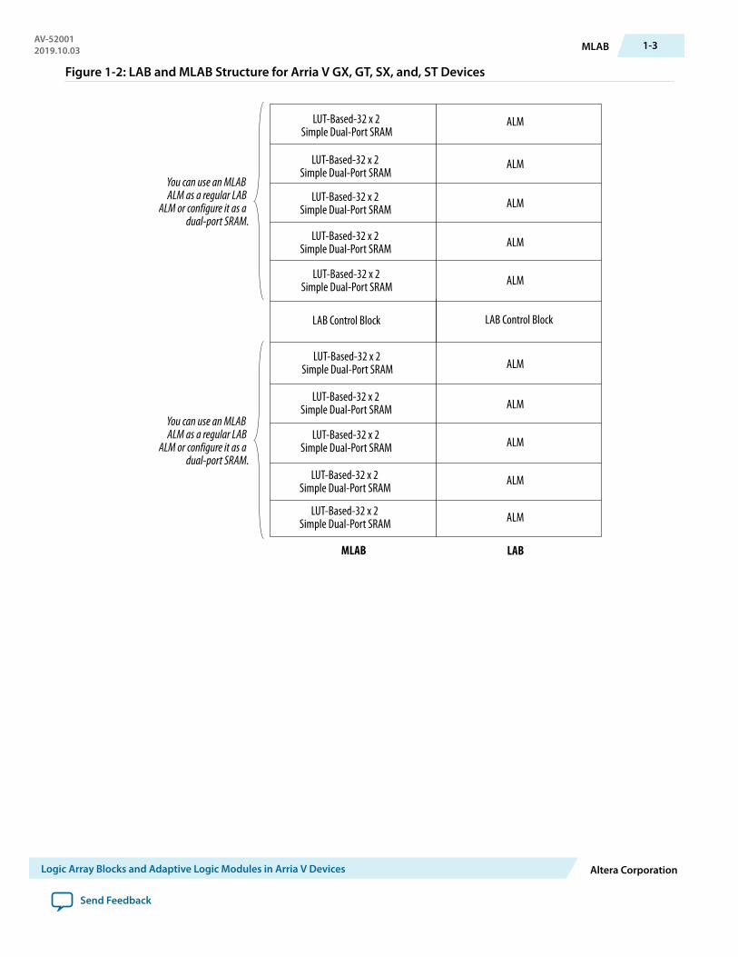
Figure 1-2: LAB and MLAB Structure for Arria V GX, GT, SX, and, ST Devices
MLAB LAB
LUT-Based-32 x 2Simple Dual-Port SRAM
LUT-Based-32 x 2Simple Dual-Port SRAM
LUT-Based-32 x 2Simple Dual-Port SRAM
LUT-Based-32 x 2Simple Dual-Port SRAM
LUT-Based-32 x 2Simple Dual-Port SRAM
LUT-Based-32 x 2Simple Dual-Port SRAM
LUT-Based-32 x 2Simple Dual-Port SRAM
LUT-Based-32 x 2Simple Dual-Port SRAM
LUT-Based-32 x 2Simple Dual-Port SRAM
LUT-Based-32 x 2Simple Dual-Port SRAM
ALM
ALM
ALM
ALM
ALM
ALM
ALM
ALM
ALM
ALM
LAB Control BlockLAB Control Block
You can use an MLAB ALM as a regular LAB
ALM or configure it as a dual-port SRAM.
You can use an MLAB ALM as a regular LAB
ALM or configure it as a dual-port SRAM.
AV-520012019.10.03 MLAB 1-3
Logic Array Blocks and Adaptive Logic Modules in Arria V Devices Altera Corporation
Send Feedback

Figure 1-3: LAB and MLAB Structure for Arria V GZ Devices
MLAB LAB
LUT-Based-64 x 1Simple Dual-Port SRAM
LUT-Based-64 x 1Simple Dual-Port SRAM
LUT-Based-64 x 1Simple Dual-Port SRAM
LUT-Based-64 x 1Simple Dual-Port SRAM
LUT-Based-64 x 1Simple Dual-Port SRAM
LUT-Based-64 x 1Simple Dual-Port SRAM
LUT-Based-64 x 1Simple Dual-Port SRAM
LUT-Based-64 x 1Simple Dual-Port SRAM
LUT-Based-64 x 1Simple Dual-Port SRAM
LUT-Based-64 x 1Simple Dual-Port SRAM
ALM
ALM
ALM
ALM
ALM
ALM
ALM
ALM
ALM
ALM
LAB Control BlockLAB Control Block
You can use an MLAB ALM as a regular LAB
ALM or configure it as a dual-port SRAM.
You can use an MLAB ALM as a regular LAB
ALM or configure it as a dual-port SRAM.
Local and Direct Link InterconnectsEach LAB can drive 30 ALMs through fast-local and direct-link interconnects. Ten ALMs are in any givenLAB and ten ALMs are in each of the adjacent LABs.
The local interconnect can drive ALMs in the same LAB using column and row interconnects and ALMoutputs in the same LAB.
Neighboring LABs, MLABs, M20K and M10K blocks, or digital signal processing (DSP) blocks from theleft or right can also drive the LAB’s local interconnect using the direct link connection.
The direct link connection feature minimizes the use of row and column interconnects, providing higherperformance and flexibility.
1-4 Local and Direct Link InterconnectsAV-52001
2019.10.03
Altera Corporation Logic Array Blocks and Adaptive Logic Modules in Arria V Devices
Send Feedback
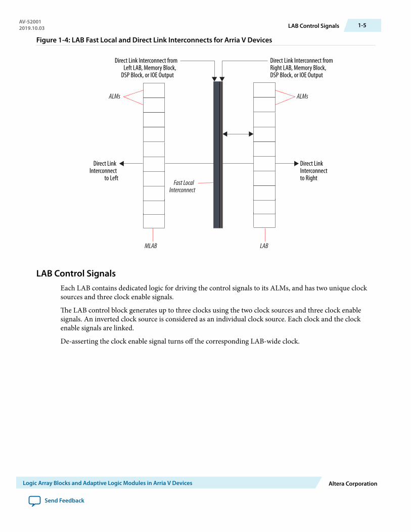
Figure 1-4: LAB Fast Local and Direct Link Interconnects for Arria V Devices
MLAB
ALMs ALMs
LAB
Fast Local Interconnect
Direct Link Interconnect from Left LAB, Memory Block,
DSP Block, or IOE Output
Direct Link Interconnect
to Left
Direct Link Interconnect to Right
Direct Link Interconnect from Right LAB, Memory Block, DSP Block, or IOE Output
LAB Control SignalsEach LAB contains dedicated logic for driving the control signals to its ALMs, and has two unique clocksources and three clock enable signals.
The LAB control block generates up to three clocks using the two clock sources and three clock enablesignals. An inverted clock source is considered as an individual clock source. Each clock and the clockenable signals are linked.
De-asserting the clock enable signal turns off the corresponding LAB-wide clock.
AV-520012019.10.03 LAB Control Signals 1-5
Logic Array Blocks and Adaptive Logic Modules in Arria V Devices Altera Corporation
Send Feedback

Figure 1-5: LAB-Wide Control Signals for Arria V GX, GT, SX, and, ST Devices
This figure shows the clock sources and clock enable signals in a LAB.
Dedicated RowLAB Clocks
Local Interconnect
Local Interconnect
Local Interconnect
Local Interconnect
labclk2 syncload
labclkena0or asyncloador labpreset
labclk0 labclk1 labclr1
labclkena1 labclkena2 labclr0 synclr
6
6
6
There are two uniqueclock signals per LAB.
1-6 LAB Control SignalsAV-52001
2019.10.03
Altera Corporation Logic Array Blocks and Adaptive Logic Modules in Arria V Devices
Send Feedback

Figure 1-6: LAB-Wide Control Signals for Arria V GZ Devices
This figure shows the clock sources and clock enable signals in a LAB.
Dedicated RowLAB Clocks
Local Interconnect
Local Interconnect
Local Interconnect
Local Interconnect
Local Interconnect
Local Interconnect
labclk2 syncloadlabclkena0
or asyncloador labpreset
labclk0 labclk1 labclr1labclkena1 labclkena2 labclr0 synclr
6
6
6
There are two uniqueclock signals per LAB.
ALM ResourcesOne ALM contains four programmable registers. Each register has the following ports:
• Data• Clock• Synchronous and asynchronous clear• Synchronous load
Global signals, general-purpose I/O (GPIO) pins, or any internal logic can drive the clock and clearcontrol signals of an ALM register.
GPIO pins or internal logic drives the clock enable signal.
For combinational functions, the registers are bypassed and the output of the look-up table (LUT) drivesdirectly to the outputs of an ALM.
Note: The Intel Quartus Prime software automatically configures the ALMs for optimized performance.
AV-520012019.10.03 ALM Resources 1-7
Logic Array Blocks and Adaptive Logic Modules in Arria V Devices Altera Corporation
Send Feedback
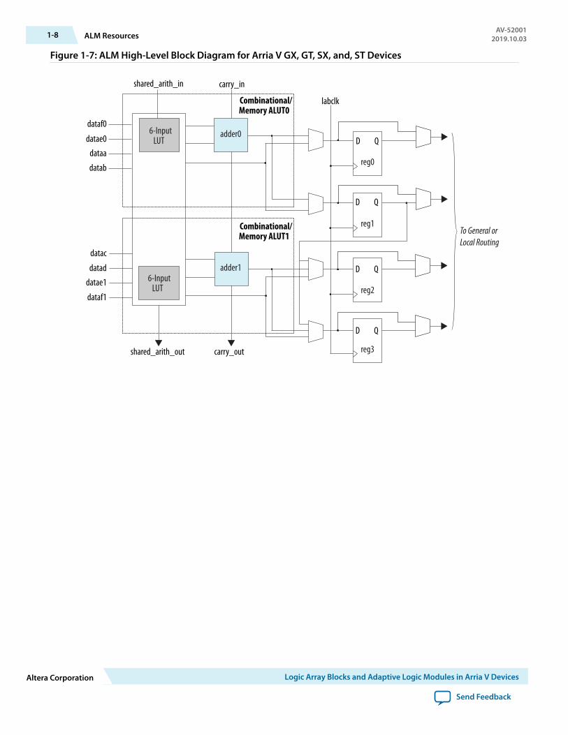
Figure 1-7: ALM High-Level Block Diagram for Arria V GX, GT, SX, and, ST Devices
datac
datad
datae1
dataf1
adder1
datae0
dataf0
dataa
datab
carry_in
carry_out
Combinational/ Memory ALUT0
6-InputLUT
6-InputLUT
shared_arith_out
shared_arith_in
Combinational/ Memory ALUT1
adder0
reg0
labclk
reg1
reg2
reg3
D Q
D Q
D Q
D Q
To General or Local Routing
1-8 ALM ResourcesAV-52001
2019.10.03
Altera Corporation Logic Array Blocks and Adaptive Logic Modules in Arria V Devices
Send Feedback

Figure 1-8: ALM High-Level Block Diagram for Arria V GZ Devices
datac
datad
datae1
dataf1
adder1
datae0
dataf0
dataa
datab
carry_in
carry_out
Combinational/Memory ALUT0
6-Input LUT
6-Input LUT
shared_arith_out
shared_arith_in
Combinational/Memory ALUT1
adder0
labclk
reg1 To General or Local Routing
reg0
reg3
reg2
ALM OutputThe general routing outputs in each ALM drive the local, row, and column routing resources. Two ALMoutputs can drive column, row, or direct link routing connections, and one of these ALM outputs can alsodrive local interconnect resources.
The LUT, adder, or register output can drive the ALM outputs. The LUT or adder can drive one outputwhile the register drives another output.
Register packing improves device utilization by allowing unrelated register and combinational logic to bepacked into a single ALM. Another mechanism to improve fitting is to allow the register output to feedback into the look-up table (LUT) of the same ALM so that the register is packed with its own fan-outLUT. The ALM can also drive out registered and unregistered versions of the LUT or adder output.
AV-520012019.10.03 ALM Output 1-9
Logic Array Blocks and Adaptive Logic Modules in Arria V Devices Altera Corporation
Send Feedback
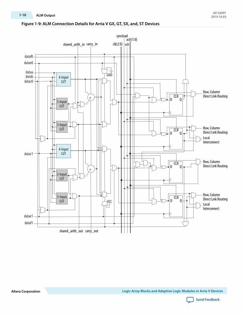
Figure 1-9: ALM Connection Details for Arria V GX, GT, SX, and, ST Devices
D QCLR
D QCLR
Row, ColumnDirect Link Routing
D QCLR
Local Interconnect
Local Interconnect
D QCLR
carry_out
GND
VCC
aclr[1:0]sclr
syncload
clk[2:0]carry_in
+
shared_arith_out
shared_arith_in
4-InputLUT
4-InputLUT
3-InputLUT
3-InputLUT
3-InputLUT
3-InputLUT
+
dataf0
datae0
dataadatab
datac1
datae1
dataf1
datac0
Row, ColumnDirect Link Routing
Row, ColumnDirect Link Routing
Row, ColumnDirect Link Routing
1-10 ALM OutputAV-52001
2019.10.03
Altera Corporation Logic Array Blocks and Adaptive Logic Modules in Arria V Devices
Send Feedback
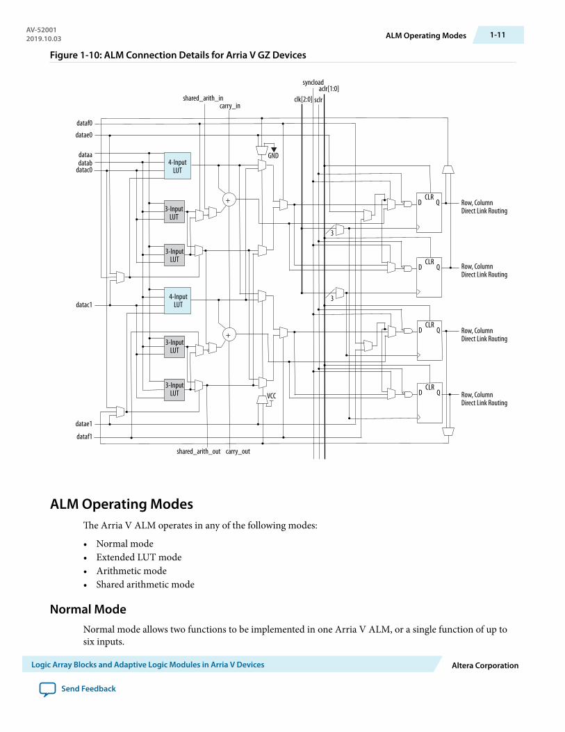
Figure 1-10: ALM Connection Details for Arria V GZ Devices
+
carry_in
dataf0
datae0
dataadatab
datac1
datae1
dataf1
shared_arith_out carry_out
shared_arith_in
4-InputLUT
4-InputLUT
3-InputLUT
3-InputLUT
3-InputLUT
3-InputLUT
+
datac0
GND
VCC
aclr[1:0]sclr
syncload
clk[2:0]
D QCLR
D QCLR
Row, ColumnDirect Link Routing
D QCLR
D QCLR
3
3
Row, ColumnDirect Link Routing
Row, ColumnDirect Link Routing
Row, ColumnDirect Link Routing
ALM Operating ModesThe Arria V ALM operates in any of the following modes:
• Normal mode• Extended LUT mode• Arithmetic mode• Shared arithmetic mode
Normal ModeNormal mode allows two functions to be implemented in one Arria V ALM, or a single function of up tosix inputs.
AV-520012019.10.03 ALM Operating Modes 1-11
Logic Array Blocks and Adaptive Logic Modules in Arria V Devices Altera Corporation
Send Feedback
Up to eight data inputs from the LAB local interconnect are inputs to the combinational logic.
The ALM can support certain combinations of completely independent functions and various combina‐tions of functions that have common inputs.
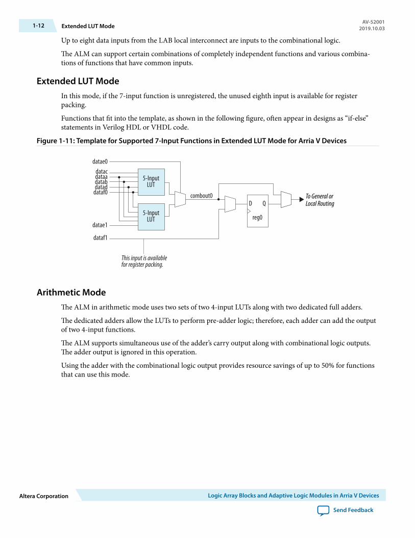
Extended LUT ModeIn this mode, if the 7-input function is unregistered, the unused eighth input is available for registerpacking.
Functions that fit into the template, as shown in the following figure, often appear in designs as “if-else”statements in Verilog HDL or VHDL code.
Figure 1-11: Template for Supported 7-Input Functions in Extended LUT Mode for Arria V Devices
datae0
combout0
5-InputLUT
5-InputLUT
datacdataadatabdatad
dataf0
datae1
dataf1
D Q
reg0
This input is availablefor register packing.
To General orLocal Routing
Arithmetic ModeThe ALM in arithmetic mode uses two sets of two 4-input LUTs along with two dedicated full adders.
The dedicated adders allow the LUTs to perform pre-adder logic; therefore, each adder can add the outputof two 4-input functions.
The ALM supports simultaneous use of the adder’s carry output along with combinational logic outputs.The adder output is ignored in this operation.
Using the adder with the combinational logic output provides resource savings of up to 50% for functionsthat can use this mode.
1-12 Extended LUT ModeAV-52001
2019.10.03
Altera Corporation Logic Array Blocks and Adaptive Logic Modules in Arria V Devices
Send Feedback

Figure 1-12: ALM in Arithmetic Mode for Arria V Devices
datae0carry_in
carry_out
dataadatabdatac
dataddatae1
4-InputLUT
4-InputLUT
4-InputLUT
4-InputLUT
adder1
dataf0
dataf1
adder0
reg1 To General orLocal Routing
reg0
reg3
reg2
Carry Chain
The carry chain provides a fast carry function between the dedicated adders in arithmetic or sharedarithmetic mode.
The two-bit carry select feature in Arria V devices halves the propagation delay of carry chains within theALM. Carry chains can begin in either the first ALM or the fifth ALM in a LAB. The final carry-out signalis routed to an ALM, where it is fed to local, row, or column interconnects.
To avoid routing congestion in one small area of the device when a high fan-in arithmetic function isimplemented, the LAB can support carry chains that only use either the top half or bottom half of the LABbefore connecting to the next LAB. This leaves the other half of the ALMs in the LAB available forimplementing narrower fan-in functions in normal mode. Carry chains that use the top five ALMs in thefirst LAB carry into the top half of the ALMs in the next LAB in the column. Carry chains that use thebottom five ALMs in the first LAB carry into the bottom half of the ALMs in the next LAB within thecolumn. You can bypass the top-half of the LAB columns and bottom-half of the MLAB columns.
The Intel Quartus Prime Compiler creates carry chains longer than 20 ALMs (10 ALMs in arithmetic orshared arithmetic mode) by linking LABs together automatically. For enhanced fitting, a long carry chainruns vertically, allowing fast horizontal connections to the TriMatrix memory and DSP blocks. A carrychain can continue as far as a full column.
Shared Arithmetic ModeThe ALM in shared arithmetic mode can implement a 3-input add in the ALM.
AV-520012019.10.03 Shared Arithmetic Mode 1-13
Logic Array Blocks and Adaptive Logic Modules in Arria V Devices Altera Corporation
Send Feedback

This mode configures the ALM with four 4-input LUTs. Each LUT either computes the sum of three inputsor the carry of three inputs. The output of the carry computation is fed to the next adder using a dedicatedconnection called the shared arithmetic chain.
Figure 1-13: ALM in Shared Arithmetic Mode for Arria V Devices
datae0
carry_in
shared_arith_in
shared_arith_out
carry_out
dataadatabdatac
dataddatae1
4-InputLUT
4-InputLUT
4-InputLUT
4-InputLUT
labclk
reg1 To General orLocal Routing
reg0
reg3
reg2
Shared Arithmetic Chain
The shared arithmetic chain available in enhanced arithmetic mode allows the ALM to implement a3-input adder. This significantly reduces the resources necessary to implement large adder trees orcorrelator functions.
The shared arithmetic chain can begin in either the first or sixth ALM in a LAB.
Similar to carry chains, the top and bottom half of the shared arithmetic chains in alternate LAB columnscan be bypassed. This capability allows the shared arithmetic chain to cascade through half of the ALMs inan LAB while leaving the other half available for narrower fan-in functionality. In every LAB, the columnis top-half bypassable; while in MLAB, columns are bottom-half bypassable.
The Intel Quartus Prime Compiler creates shared arithmetic chains longer than 20 ALMs (10 ALMs inarithmetic or shared arithmetic mode) by linking LABs together automatically. To enhance fitting, a longshared arithmetic chain runs vertically, allowing fast horizontal connections to the TriMatrix memory andDSP blocks. A shared arithmetic chain can continue as far as a full column.
1-14 Shared Arithmetic ModeAV-52001
2019.10.03
Altera Corporation Logic Array Blocks and Adaptive Logic Modules in Arria V Devices
Send Feedback

Logic Array Blocks and Adaptive Logic Modules in Arria V DevicesRevision History
Date Version Changes
December2016
2016.12.09 Added description on clock source in the LAB Control Signals section.
December2015
2015.12.21 Changed instances of Quartus II to Quartus Prime.
January 2014 2014.01.10 Added multiplexers for the bypass paths and register outputs in thefollowing diagrams:
• ALM High-Level Block Diagram for Arria V GX, GT, SX, and STDevices
• ALM High-Level Block Diagram for Arria V GZ Devices• Template for Supported 7-Input Functions in Extended LUT Mode for
Arria V Devices• ALM in Arithmetic Mode for Arria V Devices• ALM in Shared Arithmetic Mode for Arria V Devices
May 2013 2013.05.06 • Added link to the known document issues in the Knowledge Base.• Updated local and direct link interconnects section to add M20K
memory block.• Removed register chain outputs information in ALM output section.• Removed reg_chain_in and reg_chain_out ports in ALM high-
level block diagram and ALM connection details diagram forArria V GX, GT, SX, and ST devices.
November2012
2012.11.19 • Added MLAB structure for Arria V GZ devices.• Added LAB-wide control signals diagram for Arria V GZ devices.• Added ALM high level block diagram for Arria V GZ devices.• Added ALM connection details diagram for Arria V GZ devices.• Reorganized content and updated template.
June 2012 2.0 Updated for the Quartus II software v12.0 release:
• Restructured chapter.• Updated Figure 1–6.
November2011
1.1 Restructured chapter.
May 2011 1.0 Initial release.
AV-520012019.10.03 Logic Array Blocks and Adaptive Logic Modules in Arria V Devices Revision History 1-15
Logic Array Blocks and Adaptive Logic Modules in Arria V Devices Altera Corporation
Send Feedback
Embedded Memory Blocks in Arria V Devices 22019.10.03
AV-52002 Subscribe Send Feedback
The embedded memory blocks in the devices are flexible and designed to provide an optimal amount ofsmall- and large-sized memory arrays to fit your design requirements.
Related InformationArria V Device Handbook: Known IssuesLists the planned updates to the Arria V Device Handbook chapters.
Types of Embedded MemoryThe Arria V devices contain two types of memory blocks:
• 20 Kb M20K or 10 Kb M10K blocks—blocks of dedicated memory resources. The M20K and M10Kblocks are ideal for larger memory arrays while still providing a large number of independent ports.
• 640 bit memory logic array blocks (MLABs)—enhanced memory blocks that are configured from dual-purpose logic array blocks (LABs). The MLABs are ideal for wide and shallow memory arrays. TheMLABs are optimized for implementation of shift registers for digital signal processing (DSP) applica‐tions, wide shallow FIFO buffers, and filter delay lines. Each MLAB is made up of ten adaptive logicmodules (ALMs). In the Arria V devices, you can configure these ALMs as ten 32 x 2 blocks, giving youone 32 x 20 simple dual-port SRAM block per MLAB. You can also configure these ALMs, in Arria VGZ devices, as ten 64 x 1 blocks, giving you one 64 x 10 simple dual-port SRAM block per MLAB.
Intel Corporation. All rights reserved. Intel, the Intel logo, Altera, Arria, Cyclone, Enpirion, MAX, Nios, Quartus and Stratix words and logos are trademarks ofIntel Corporation or its subsidiaries in the U.S. and/or other countries. Intel warrants performance of its FPGA and semiconductor products to currentspecifications in accordance with Intel's standard warranty, but reserves the right to make changes to any products and services at any time without notice.Intel assumes no responsibility or liability arising out of the application or use of any information, product, or service described herein except as expresslyagreed to in writing by Intel. Intel customers are advised to obtain the latest version of device specifications before relying on any published informationand before placing orders for products or services.*Other names and brands may be claimed as the property of others.
ISO9001:2015Registered
www.altera.com101 Innovation Drive, San Jose, CA 95134
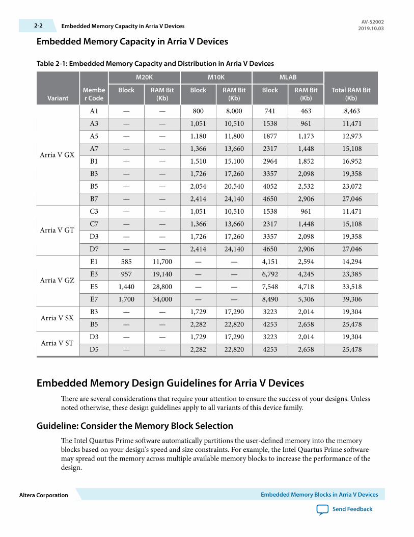
Embedded Memory Capacity in Arria V Devices
Table 2-1: Embedded Memory Capacity and Distribution in Arria V Devices
VariantMember Code
M20K M10K MLAB
Total RAM Bit(Kb)
Block RAM Bit(Kb)
Block RAM Bit(Kb)
Block RAM Bit(Kb)
Arria V GX
A1 — — 800 8,000 741 463 8,463A3 — — 1,051 10,510 1538 961 11,471A5 — — 1,180 11,800 1877 1,173 12,973A7 — — 1,366 13,660 2317 1,448 15,108B1 — — 1,510 15,100 2964 1,852 16,952B3 — — 1,726 17,260 3357 2,098 19,358B5 — — 2,054 20,540 4052 2,532 23,072B7 — — 2,414 24,140 4650 2,906 27,046
Arria V GT
C3 — — 1,051 10,510 1538 961 11,471C7 — — 1,366 13,660 2317 1,448 15,108D3 — — 1,726 17,260 3357 2,098 19,358D7 — — 2,414 24,140 4650 2,906 27,046
Arria V GZ
E1 585 11,700 — — 4,151 2,594 14,294E3 957 19,140 — — 6,792 4,245 23,385E5 1,440 28,800 — — 7,548 4,718 33,518E7 1,700 34,000 — — 8,490 5,306 39,306
Arria V SXB3 — — 1,729 17,290 3223 2,014 19,304B5 — — 2,282 22,820 4253 2,658 25,478
Arria V STD3 — — 1,729 17,290 3223 2,014 19,304D5 — — 2,282 22,820 4253 2,658 25,478
Embedded Memory Design Guidelines for Arria V DevicesThere are several considerations that require your attention to ensure the success of your designs. Unlessnoted otherwise, these design guidelines apply to all variants of this device family.
Guideline: Consider the Memory Block SelectionThe Intel Quartus Prime software automatically partitions the user-defined memory into the memoryblocks based on your design's speed and size constraints. For example, the Intel Quartus Prime softwaremay spread out the memory across multiple available memory blocks to increase the performance of thedesign.
2-2 Embedded Memory Capacity in Arria V DevicesAV-52002
2019.10.03
Altera Corporation Embedded Memory Blocks in Arria V Devices
Send Feedback

To assign the memory to a specific block size manually, use the RAM IP core in the IP Catalog.
For the memory logic array blocks (MLAB), you can implement single-port SRAM through emulationusing the Intel Quartus Prime software. Emulation results in minimal additional use of logic resources.
Because of the dual-purpose architecture of the MLAB, only data input and output registers are availablein the block. The MLABs gain read address registers from the ALMs. However, the write address and readdata registers are internal to the MLABs.
Guideline: Implement External Conflict ResolutionIn the true dual-port RAM mode, you can perform two write operations to the same memory location.However, the memory blocks do not have internal conflict resolution circuitry. To avoid unknown databeing written to the address, implement external conflict resolution logic to the memory block.
Guideline: Customize Read-During-Write BehaviorCustomize the read-during-write behavior of the memory blocks to suit your design requirements.
Figure 2-1: Read-During-Write Data Flow
This figure shows the difference between the two types of read-during-write operations available—sameport and mixed port.
Port Adata in
Port Bdata in
Port Adata out
Port Bdata out
Mixed-portdata flowSame-portdata flow
FPGA Device
Same-Port Read-During-Write Mode
The same-port read-during-write mode applies to a single-port RAM or the same port of a true dual-portRAM.
Table 2-2: Output Modes for Embedded Memory Blocks in Same-Port Read-During-Write Mode
This table lists the available output modes if you select the embedded memory blocks in the same-portread-during-write mode.
Output Mode Memory Type Description
"new data"
(flow-through)
M20K, M10K The new data is available on the rising edge of thesame clock cycle on which the new data is written.
"don't care" M10K, MLAB The RAM outputs "don't care" values for a read-during-write operation.
AV-520022019.10.03 Guideline: Implement External Conflict Resolution 2-3
Embedded Memory Blocks in Arria V Devices Altera Corporation
Send Feedback
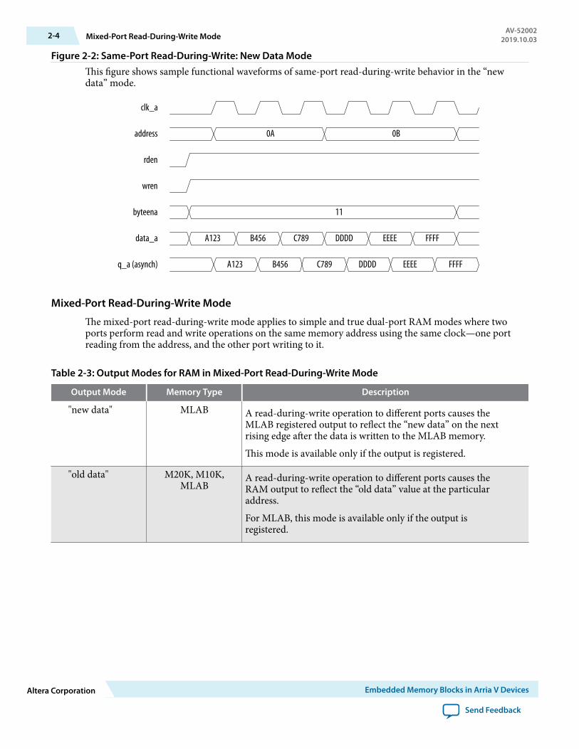
Figure 2-2: Same-Port Read-During-Write: New Data ModeThis figure shows sample functional waveforms of same-port read-during-write behavior in the “newdata” mode.
clk_a
address
rden
wren
byteena
data_a
q_a (asynch)
A123 B456 C789 DDDD EEEE FFFF
A123 B456 C789 DDDD EEEE FFFF
0A 0B
11
Mixed-Port Read-During-Write Mode
The mixed-port read-during-write mode applies to simple and true dual-port RAM modes where twoports perform read and write operations on the same memory address using the same clock—one portreading from the address, and the other port writing to it.
Table 2-3: Output Modes for RAM in Mixed-Port Read-During-Write Mode
Output Mode Memory Type Description
"new data" MLAB A read-during-write operation to different ports causes theMLAB registered output to reflect the “new data” on the nextrising edge after the data is written to the MLAB memory.
This mode is available only if the output is registered.
"old data" M20K, M10K,MLAB
A read-during-write operation to different ports causes theRAM output to reflect the “old data” value at the particularaddress.
For MLAB, this mode is available only if the output isregistered.
2-4 Mixed-Port Read-During-Write ModeAV-52002
2019.10.03
Altera Corporation Embedded Memory Blocks in Arria V Devices
Send Feedback

Output Mode Memory Type Description
"don't care" M20K, M10K,MLAB
The RAM outputs “don’t care” or “unknown” value.
• For M20K or M10K memory, the Intel Quartus Primesoftware does not analyze the timing between write and readoperations.
• For MLAB, the Intel Quartus Prime software analyzes thetiming between write and read operations by default. Todisable this behavior, turn on the Do not analyze the timingbetween write and read operation. Metastability issues areprevented by never writing and reading at the sameaddress at the same time option.
"constraineddon't care"
MLAB The RAM outputs “don’t care” or “unknown” value. The IntelQuartus Prime software analyzes the timing between write andread operations in the MLAB.
Figure 2-3: Mixed-Port Read-During-Write: New Data ModeThis figure shows a sample functional waveform of mixed-port read-during-write behavior for the “newdata” mode.
XXXX
11
clk_a&b
address_a
wren_a
byteena_a
rden_b
data_a
q_b (registered)
address_b
AAAA BBBB CCCC DDDD EEEE FFFF
A0 A1
A0 A1
AAAA BBBB CCCC DDDD EEEE FFFF
AV-520022019.10.03 Mixed-Port Read-During-Write Mode 2-5
Embedded Memory Blocks in Arria V Devices Altera Corporation
Send Feedback
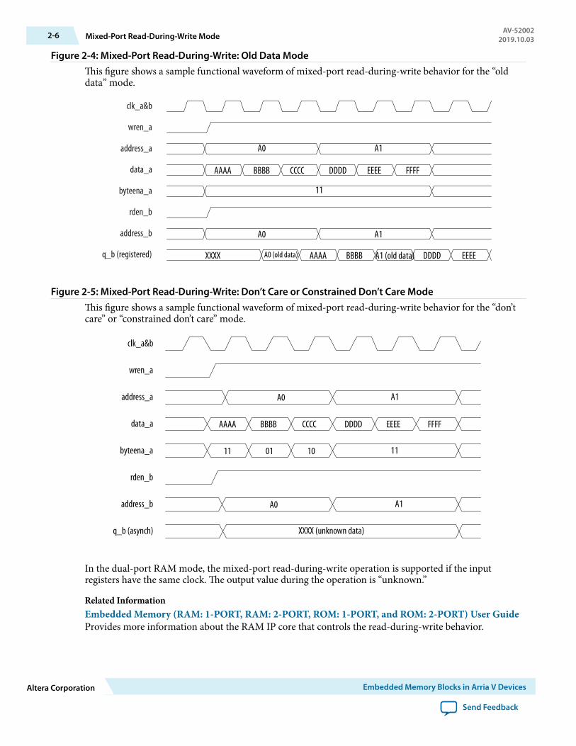
Figure 2-4: Mixed-Port Read-During-Write: Old Data ModeThis figure shows a sample functional waveform of mixed-port read-during-write behavior for the “olddata” mode.
XXXX
11
clk_a&b
address_a
wren_a
byteena_a
rden_b
data_a
q_b (registered)
address_b
AAAA BBBB CCCC DDDD EEEE FFFF
A0 A1
A0 A1
AAAA BBBB A1 (old data) DDDD EEEEA0 (old data)
Figure 2-5: Mixed-Port Read-During-Write: Don’t Care or Constrained Don’t Care ModeThis figure shows a sample functional waveform of mixed-port read-during-write behavior for the “don’tcare” or “constrained don’t care” mode.
clk_a&b
wren_a
address_a A0 A1
data_a
byteena_a
rden_b
address_b
q_b (asynch) XXXX (unknown data)
A0 A1
11 1101 10
AAAA BBBB CCCC DDDD EEEE FFFF
In the dual-port RAM mode, the mixed-port read-during-write operation is supported if the inputregisters have the same clock. The output value during the operation is “unknown.”
Related InformationEmbedded Memory (RAM: 1-PORT, RAM: 2-PORT, ROM: 1-PORT, and ROM: 2-PORT) User GuideProvides more information about the RAM IP core that controls the read-during-write behavior.
2-6 Mixed-Port Read-During-Write ModeAV-52002
2019.10.03
Altera Corporation Embedded Memory Blocks in Arria V Devices
Send Feedback

Guideline: Consider Power-Up State and Memory InitializationConsider the power up state of the different types of memory blocks if you are designing logic thatevaluates the initial power-up values, as listed in the following table.
Table 2-4: Initial Power-Up Values of Embedded Memory Blocks
Memory Type Output Registers Power Up Value
MLABUsed Zero (cleared)
Bypassed Read memory contents
M20K, M10KUsed Zero (cleared)
Bypassed Zero (cleared)
By default, the Intel Quartus Prime software initializes the RAM cells in Arria V devices to zero unless youspecify a .mif.
All memory blocks support initialization with a .mif. You can create .mif files in the Intel Quartus Primesoftware and specify their use with the RAM IP core when you instantiate a memory in your design. Evenif a memory is pre-initialized (for example, using a .mif), it still powers up with its output cleared.
Related Information
• Embedded Memory (RAM: 1-PORT, RAM: 2-PORT, ROM: 1-PORT, and ROM: 2-PORT) UserGuideProvides more information about .mif files.
• Quartus II HandbookProvides more information about .mif files.
Guideline: Control Clocking to Reduce Power ConsumptionReduce AC power consumption in your design by controlling the clocking of each memory block:
• Use the read-enable signal to ensure that read operations occur only when necessary. If your designdoes not require read-during-write, you can reduce your power consumption by de-asserting the read-enable signal during write operations, or during the period when no memory operations occur.
• Use the Intel Quartus Prime software to automatically place any unused memory blocks in low-powermode to reduce static power.
Embedded Memory Features
Table 2-5: Memory Features in Arria V Devices
This table summarizes the features supported by the embedded memory blocks.
AV-520022019.10.03 Guideline: Consider Power-Up State and Memory Initialization 2-7
Embedded Memory Blocks in Arria V Devices Altera Corporation
Send Feedback
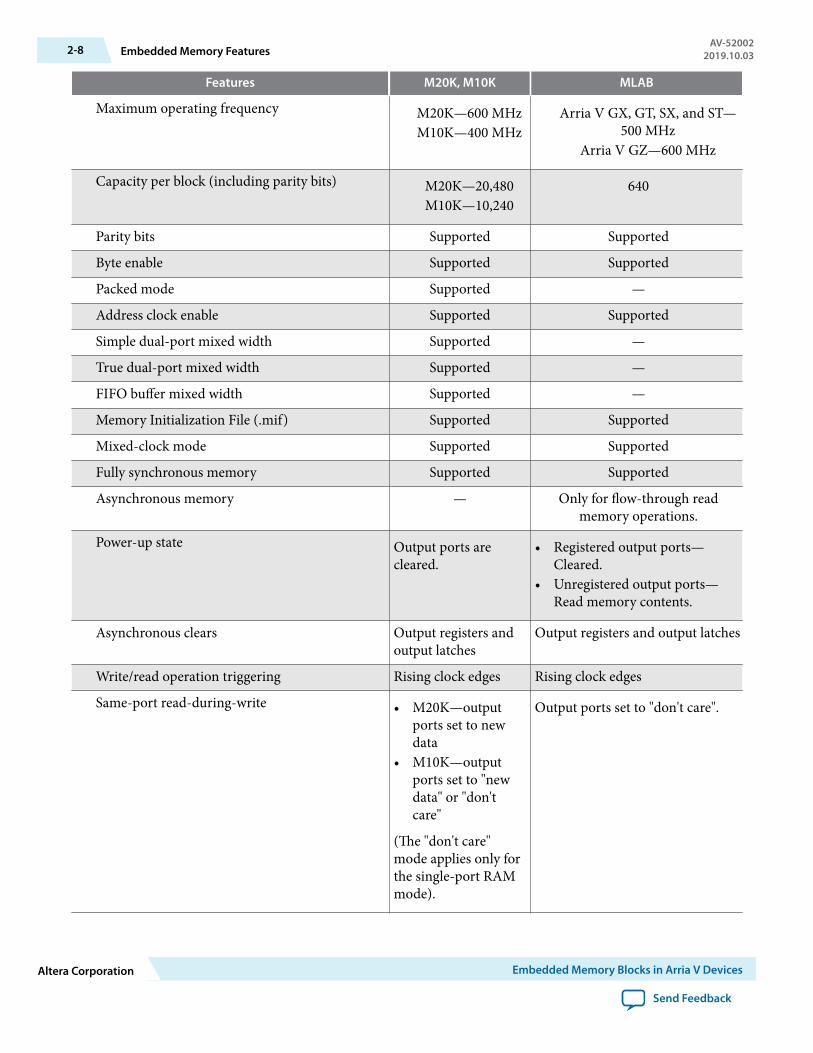
Features M20K, M10K MLAB
Maximum operating frequency M20K—600 MHzM10K—400 MHz
Arria V GX, GT, SX, and ST—500 MHz
Arria V GZ—600 MHz
Capacity per block (including parity bits) M20K—20,480M10K—10,240
640
Parity bits Supported Supported
Byte enable Supported Supported
Packed mode Supported —
Address clock enable Supported Supported
Simple dual-port mixed width Supported —
True dual-port mixed width Supported —
FIFO buffer mixed width Supported —
Memory Initialization File (.mif) Supported Supported
Mixed-clock mode Supported Supported
Fully synchronous memory Supported Supported
Asynchronous memory — Only for flow-through readmemory operations.
Power-up state Output ports arecleared.
• Registered output ports—Cleared.
• Unregistered output ports—Read memory contents.
Asynchronous clears Output registers andoutput latches
Output registers and output latches
Write/read operation triggering Rising clock edges Rising clock edges
Same-port read-during-write • M20K—outputports set to newdata
• M10K—outputports set to "newdata" or "don'tcare"
(The "don't care"mode applies only forthe single-port RAMmode).
Output ports set to "don't care".
2-8 Embedded Memory FeaturesAV-52002
2019.10.03
Altera Corporation Embedded Memory Blocks in Arria V Devices
Send Feedback

Features M20K, M10K MLAB
Mixed-port read-during-write Output ports set to"old data" or "don'tcare".
Output ports set to "old data", "newdata", "don't care", or "constraineddon't care".
ECC support Soft IP support usingthe Intel QuartusPrime software.
Built-in support inx32-wide simple dual-port mode (M20Konly).
Soft IP support using the IntelQuartus Prime software.
Related InformationEmbedded Memory (RAM: 1-PORT, RAM: 2-PORT, ROM: 1-PORT, and ROM: 2-PORT) User GuideProvides more information about the embedded memory features.
Embedded Memory Configurations
Table 2-6: Supported Embedded Memory Block Configurations for Arria V Devices
This table lists the maximum configurations supported for the embedded memory blocks. Theinformation is applicable only to the single-port RAM and ROM modes.
Memory Block Depth (bits) Programmable Width
MLAB32 x16, x18, or x20
64(1) x10
M20K
512 x401K x202K x104K x58K x2
16K x1
M10K
256 x40 or x32512 x20 or x161K x10 or x82K x5 or x44K x28K x1
(1) Available for Arria V GZ devices only.
AV-520022019.10.03 Embedded Memory Configurations 2-9
Embedded Memory Blocks in Arria V Devices Altera Corporation
Send Feedback
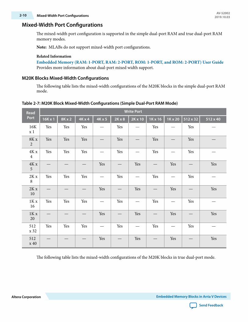
Mixed-Width Port ConfigurationsThe mixed-width port configuration is supported in the simple dual-port RAM and true dual-port RAMmemory modes.
Note: MLABs do not support mixed-width port configurations.
Related InformationEmbedded Memory (RAM: 1-PORT, RAM: 2-PORT, ROM: 1-PORT, and ROM: 2-PORT) User GuideProvides more information about dual-port mixed width support.
M20K Blocks Mixed-Width Configurations
The following table lists the mixed-width configurations of the M20K blocks in the simple dual-port RAMmode.
Table 2-7: M20K Block Mixed-Width Configurations (Simple Dual-Port RAM Mode)
ReadPort
Write Port
16K x 1 8K x 2 4K x 4 4K x 5 2K x 8 2K x 10 1K x 16 1K x 20 512 x 32 512 x 40
16K x 1
Yes Yes Yes — Yes — Yes — Yes —
8K x 2
Yes Yes Yes — Yes — Yes — Yes —
4K x 4
Yes Yes Yes — Yes — Yes — Yes —
4K x 5
— — — Yes — Yes — Yes — Yes
2K x 8
Yes Yes Yes — Yes — Yes — Yes —
2K x 10
— — — Yes — Yes — Yes — Yes
1K x 16
Yes Yes Yes — Yes — Yes — Yes —
1K x 20
— — — Yes — Yes — Yes — Yes
512 x 32
Yes Yes Yes — Yes — Yes — Yes —
512 x 40
— — — Yes — Yes — Yes — Yes
The following table lists the mixed-width configurations of the M20K blocks in true dual-port mode.
2-10 Mixed-Width Port ConfigurationsAV-52002
2019.10.03
Altera Corporation Embedded Memory Blocks in Arria V Devices
Send Feedback
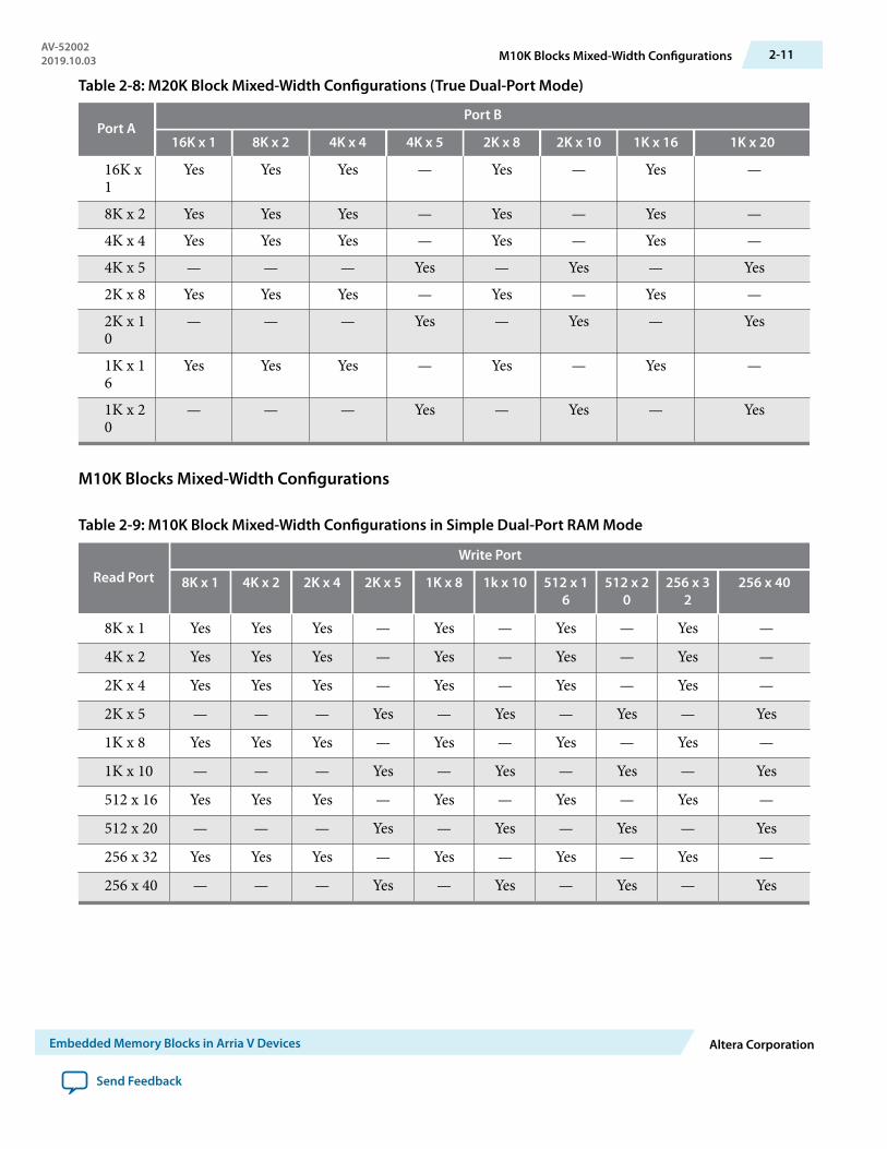
Table 2-8: M20K Block Mixed-Width Configurations (True Dual-Port Mode)
Port APort B
16K x 1 8K x 2 4K x 4 4K x 5 2K x 8 2K x 10 1K x 16 1K x 20
16K x 1
Yes Yes Yes — Yes — Yes —
8K x 2 Yes Yes Yes — Yes — Yes —4K x 4 Yes Yes Yes — Yes — Yes —4K x 5 — — — Yes — Yes — Yes2K x 8 Yes Yes Yes — Yes — Yes —2K x 10
— — — Yes — Yes — Yes
1K x 16
Yes Yes Yes — Yes — Yes —
1K x 20
— — — Yes — Yes — Yes
M10K Blocks Mixed-Width Configurations
Table 2-9: M10K Block Mixed-Width Configurations in Simple Dual-Port RAM Mode
Read Port
Write Port
8K x 1 4K x 2 2K x 4 2K x 5 1K x 8 1k x 10 512 x 16
512 x 20
256 x 32
256 x 40
8K x 1 Yes Yes Yes — Yes — Yes — Yes —
4K x 2 Yes Yes Yes — Yes — Yes — Yes —
2K x 4 Yes Yes Yes — Yes — Yes — Yes —
2K x 5 — — — Yes — Yes — Yes — Yes
1K x 8 Yes Yes Yes — Yes — Yes — Yes —
1K x 10 — — — Yes — Yes — Yes — Yes
512 x 16 Yes Yes Yes — Yes — Yes — Yes —
512 x 20 — — — Yes — Yes — Yes — Yes
256 x 32 Yes Yes Yes — Yes — Yes — Yes —
256 x 40 — — — Yes — Yes — Yes — Yes
AV-520022019.10.03 M10K Blocks Mixed-Width Configurations 2-11
Embedded Memory Blocks in Arria V Devices Altera Corporation
Send Feedback

Table 2-10: M10K Block Mixed-Width Configurations in True Dual-Port Mode
Port BPort A
8K x 1 4K x 2 2K x 4 2K x 5 1K x 8 1K x 10 512 x 16 512 x 20
8K x 1 Yes Yes Yes — Yes — Yes —
4K x 2 Yes Yes Yes — Yes — Yes —
2K x 4 Yes Yes Yes — Yes — Yes —
2K x 5 — — — Yes — Yes — Yes
1K x 8 Yes Yes Yes — Yes — Yes —
1K x 10 — — — Yes — Yes — Yes
512 x 16 Yes Yes Yes — Yes — Yes —
512 x 20 — — — Yes — Yes — Yes
Embedded Memory ModesCaution: To avoid corrupting the memory contents, do not violate the setup or hold time on any of the
memory block input registers during read or write operations. This is applicable if you use thememory blocks in single-port RAM, simple dual-port RAM, true dual-port RAM, or ROMmode.
Table 2-11: Memory Modes Supported in the Embedded Memory Blocks
This table lists and describes the memory modes that are supported in the Arria V embedded memoryblocks.
Memory Mode
M20Kand
M10KSupport
MLABSupport Description
Single-port RAM Yes Yes You can perform only one read or one write operation at a time.
Use the read enable port to control the RAM output portsbehavior during a write operation:
• To retain the previous values that are held during the mostrecent active read enable—create a read-enable port andperform the write operation with the read enable portdeasserted.
• To show the new data being written, the old data at thataddress, or a "Don't Care" value when read-during-writeoccurs at the same address location—do not create a read-enable signal, or activate the read enable during a writeoperation.
2-12 Embedded Memory ModesAV-52002
2019.10.03
Altera Corporation Embedded Memory Blocks in Arria V Devices
Send Feedback

Memory Mode
M20Kand
M10KSupport
MLABSupport Description
Simple dual-portRAM
Yes Yes You can simultaneously perform one read and one writeoperations to different locations where the write operationhappens on port A and the read operation happens on port B.
True dual-portRAM
Yes — You can perform any combination of two port operations: tworeads, two writes, or one read and one write at two differentclock frequencies.
Shift-register Yes Yes You can use the memory blocks as a shift-register block to savelogic cells and routing resources.
This is useful in DSP applications that require local data storagesuch as finite impulse response (FIR) filters, pseudo-randomnumber generators, multi-channel filtering, and auto- andcross- correlation functions. Traditionally, the local data storageis implemented with standard flip-flops that exhaust many logiccells for large shift registers.
The input data width (w), the length of the taps (m), and thenumber of taps (n) determine the size of a shift register(w × m × n). You can cascade memory blocks to implementlarger shift registers.
ROM Yes Yes You can use the memory blocks as ROM.
• Initialize the ROM contents of the memory blocks usinga .mif or .hex.
• The address lines of the ROM are registered on M20K orM10K blocks but can be unregistered on MLABs.
• The outputs can be registered or unregistered.• The output registers can be asynchronously cleared.• The ROM read operation is identical to the read operation in
the single-port RAM configuration.
FIFO Yes Yes You can use the memory blocks as FIFO buffers. Use theSCFIFO and DCFIFO IP cores to implement single- and dual-clock asynchronous FIFO buffers in your design.
For designs with many small and shallow FIFO buffers, theMLABs are ideal for the FIFO mode. However, the MLABs donot support mixed-width FIFO mode.
Related Information
• Embedded Memory (RAM: 1-PORT, RAM: 2-PORT, ROM: 1-PORT, and ROM: 2-PORT) UserGuideProvides more information memory modes.
AV-520022019.10.03 Embedded Memory Modes 2-13
Embedded Memory Blocks in Arria V Devices Altera Corporation
Send Feedback
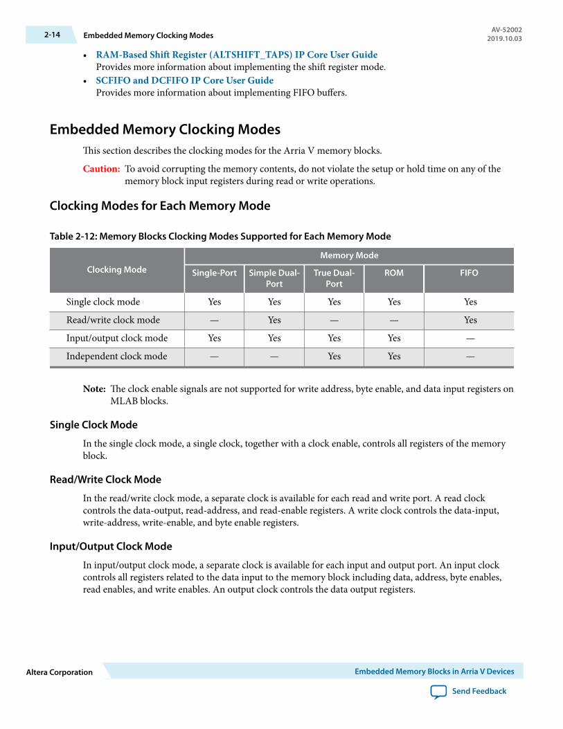
• RAM-Based Shift Register (ALTSHIFT_TAPS) IP Core User GuideProvides more information about implementing the shift register mode.
• SCFIFO and DCFIFO IP Core User GuideProvides more information about implementing FIFO buffers.
Embedded Memory Clocking ModesThis section describes the clocking modes for the Arria V memory blocks.
Caution: To avoid corrupting the memory contents, do not violate the setup or hold time on any of thememory block input registers during read or write operations.
Clocking Modes for Each Memory Mode
Table 2-12: Memory Blocks Clocking Modes Supported for Each Memory Mode
Clocking Mode
Memory Mode
Single-Port Simple Dual-Port
True Dual-Port
ROM FIFO
Single clock mode Yes Yes Yes Yes Yes
Read/write clock mode — Yes — — Yes
Input/output clock mode Yes Yes Yes Yes —
Independent clock mode — — Yes Yes —
Note: The clock enable signals are not supported for write address, byte enable, and data input registers onMLAB blocks.
Single Clock Mode
In the single clock mode, a single clock, together with a clock enable, controls all registers of the memoryblock.
Read/Write Clock Mode
In the read/write clock mode, a separate clock is available for each read and write port. A read clockcontrols the data-output, read-address, and read-enable registers. A write clock controls the data-input,write-address, write-enable, and byte enable registers.
Input/Output Clock Mode
In input/output clock mode, a separate clock is available for each input and output port. An input clockcontrols all registers related to the data input to the memory block including data, address, byte enables,read enables, and write enables. An output clock controls the data output registers.
2-14 Embedded Memory Clocking ModesAV-52002
2019.10.03
Altera Corporation Embedded Memory Blocks in Arria V Devices
Send Feedback

Independent Clock Mode
In the independent clock mode, a separate clock is available for each port (A and B). Clock A controls allregisters on the port A side; clock B controls all registers on the port B side.
Note: You can create independent clock enable for different input and output registers to control the shutdown of a particular register for power saving purposes. From the parameter editor, click MoreOptions (beside the clock enable option) to set the available independent clock enable that youprefer.
Asynchronous Clears in Clocking ModesIn all clocking modes, asynchronous clears are available only for output latches and output registers. Forthe independent clock mode, this is applicable on both ports.
Output Read Data in Simultaneous Read/WriteIf you perform a simultaneous read/write to the same address location using the read/write clock mode,the output read data is unknown. If you require the output read data to be a known value, use single-clockor input/output clock mode and select the appropriate read-during-write behavior in the IP Catalog.
Note: MLAB memory blocks only support simultaneous read/write operations when operating in singleclock mode.
Independent Clock Enables in Clocking ModesIndependent clock enables are supported in the following clocking modes:
• Read/write clock mode—supported for both the read and write clocks.• Independent clock mode—supported for the registers of both ports.
To save power, you can control the shut down of a particular register using the clock enables.
Related InformationGuideline: Control Clocking to Reduce Power Consumption on page 2-7
Parity Bit in Memory Blocks
Table 2-13: Parity Bit Support for the Embedded Memory Blocks
This table describes the parity bit support for the memory blocks.M20K, M10K MLAB
• The parity bit is the fifth bit associated with each4 data bits in data widths of 5, 10, 20, and 40 (bits4, 9, 14, 19, 24, 29, 34, and 39).
• In non-parity data widths, the parity bits areskipped during read or write operations.
• Parity function is not performed on the paritybit.
• The parity bit is the ninth bit associated witheach byte.
• The ninth bit can store a parity bit or serve as anadditional bit.
• Parity function is not performed on the paritybit.
AV-520022019.10.03 Independent Clock Mode 2-15
Embedded Memory Blocks in Arria V Devices Altera Corporation
Send Feedback
Byte Enable in Embedded Memory BlocksThe embedded memory blocks support byte enable controls:
• The byte enable controls mask the input data so that only specific bytes of data are written. Theunwritten bytes retain the values written previously.
• The write enable (wren) signal, together with the byte enable (byteena) signal, control the writeoperations on the RAM blocks. By default, the byteena signal is high (enabled) and only the wrensignal controls the writing.
• The byte enable registers do not have a clear port.• If you are using parity bits, on the M20K and M10K blocks, the byte enable function controls 8 data
bits and 2 parity bits; on the MLABs, the byte enable function controls all 10 bits in the widest mode.• The MSB and LSB of the byteena signal correspond to the MSB and LSB of the data bus, respectively.• The byte enables are active high.
Byte Enable Controls in Memory Blocks
Table 2-14: byteena Controls in x20 Data Width
byteena[1:0] Data Bits Written
11 (default) [19:10] [9:0]
10 [19:10] —01 — [9:0]
Table 2-15: byteena Controls in x40 Data Width
byteena[3:0] Data Bits Written
1111 (default) [39:30] [29:20] [19:10] [9:0]
1000 [39:30] — — —0100 — [29:20] — —0010 — — [19:10] —0001 — — — [9:0]
Note: If you use the ECC feature on the M20K blocks, you cannot use the byte enable feature.
Data Byte OutputIn M10K blocks, the corresponding masked data byte output appears as a “don’t care” value.
In M20K blocks or MLABs, when you de-assert a byte-enable bit during a write cycle, the correspondingdata byte output appears as either a “don't care” value or the current data at that location. You can controlthe output value for the masked byte in the M20K blocks or MLABs by using the Intel Quartus Primesoftware.
2-16 Byte Enable in Embedded Memory BlocksAV-52002
2019.10.03
Altera Corporation Embedded Memory Blocks in Arria V Devices
Send Feedback

RAM Blocks OperationsFigure 2-6: Byte Enable Functional Waveform
This figure shows how the wren and byteena signals control the operations of the RAM blocks. For theM10K blocks, the write-masked data byte output appears as a “don’t care” value because the “current data”value is not supported.
inclock
wren
address
data
byteena
contents at a0
contents at a1
contents at a2
contents at a3
contents at a4
don’t care: q (asynch)
current data: q (asynch)
an a0 a1 a2 a3 a4 a0
XXXXXXXX XXXXXXXXABCDEF12
ABCDEF12
XXXX XXXX1000 0100 0010 0001 1111
FFFFFFFF
FFFFFFFF
FFFFFFFF
FFFFFFFF
FFFFFFFF
FFFFFF12
FFFFFF12
FFFFEFFF
FFFFEFFF
FFCDFFFF
FFCDFFFF
ABFFFFFF
ABFFFFFF
ABFFFFFFdoutn
doutn
ABXXXXXX XXCDXXXX XXXXEFXX XXXXXX12 ABCDEF12
ABFFFFFFABCDEF12
Memory Blocks Packed Mode SupportThe M20K and M10K memory blocks support packed mode.
The packed mode feature packs two independent single-port RAM blocks into one memory block. TheIntel Quartus Prime software automatically implements packed mode where appropriate by placing thephysical RAM block in true dual-port mode and using the MSB of the address to distinguish between thetwo logical RAM blocks. The size of each independent single-port RAM must not exceed half of the targetblock size.
Memory Blocks Address Clock Enable SupportThe embedded memory blocks support address clock enable, which holds the previous address value for aslong as the signal is enabled (addressstall = 1). When the memory blocks are configured in dual-portmode, each port has its own independent address clock enable. The default value for the address clockenable signal is low (disabled).
AV-520022019.10.03 RAM Blocks Operations 2-17
Embedded Memory Blocks in Arria V Devices Altera Corporation
Send Feedback
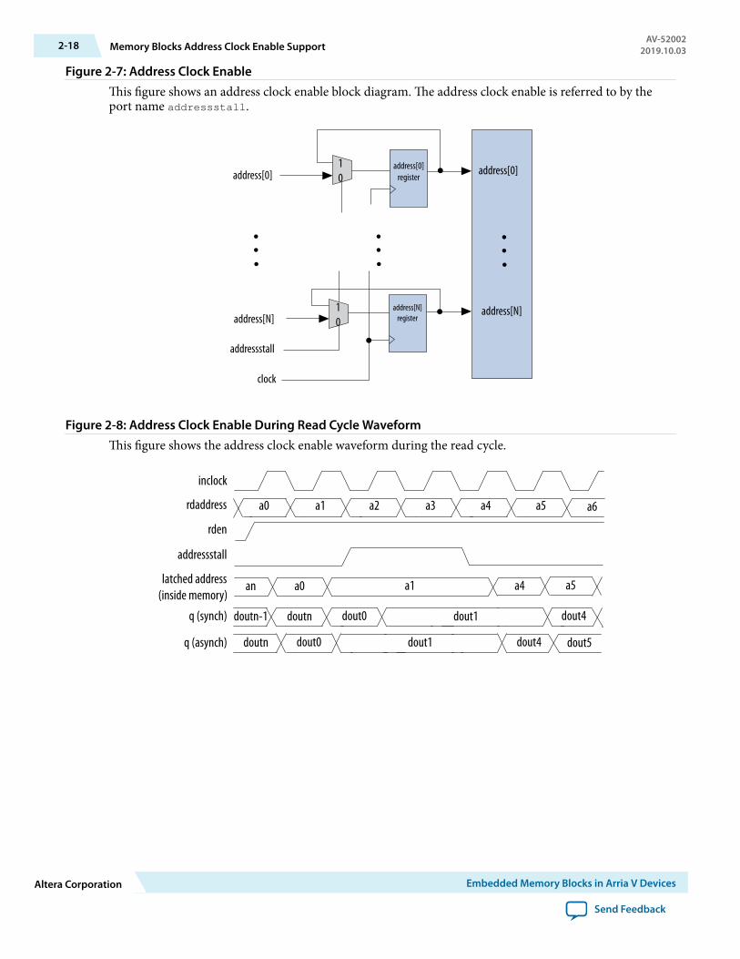
Figure 2-7: Address Clock EnableThis figure shows an address clock enable block diagram. The address clock enable is referred to by theport name addressstall.
address[0]
address[N]
addressstall
clock
10
address[0]register
address[N]register
address[N]
address[0]
10
Figure 2-8: Address Clock Enable During Read Cycle WaveformThis figure shows the address clock enable waveform during the read cycle.
inclock
rden
rdaddress
q (synch)
a0 a1 a2 a3 a4 a5 a6
q (asynch)
an a0 a4 a5latched address(inside memory)
dout0 dout1 dout4
dout4 dout5
addressstall
a1
doutn-1 doutn
doutn dout0 dout1
2-18 Memory Blocks Address Clock Enable SupportAV-52002
2019.10.03
Altera Corporation Embedded Memory Blocks in Arria V Devices
Send Feedback

Figure 2-9: Address Clock Enable During the Write Cycle WaveformThis figure shows the address clock enable waveform during the write cycle.
inclock
wren
wraddress a0 a1 a2 a3 a4 a5 a6
an a0 a4 a5latched address(inside memory)
addressstall
a1
data 00 01 02 03 04 05 06
contents at a0
contents at a1
contents at a2
contents at a3
contents at a4
contents at a5
XX
04XX
00
0301XX 02
XX
XX
XX 05
Memory Blocks Error Correction Code SupportECC allows you to detect and correct data errors at the output of the memory. ECC can perform single-error correction, double-adjacent-error correction, and triple-adjacent-error detection in a 32-bit word.However, ECC cannot detect four or more errors.
The M20K blocks have built-in support for ECC when in x32-wide simple dual-port mode:
• The M20K runs slower than non-ECC simple-dual port mode when ECC is engaged. However, you canenable optional ECC pipeline registers before the output decoder to achieve the same performance asnon-ECC simple-dual port mode at the expense of one cycle of latency.
• The M20K ECC status is communicated with two ECC status flag signals—e (error) and ue (uncorrect‐able error). The status flags are part of the regular output from the memory block. When ECC isengaged, you cannot access two of the parity bits because the ECC status flag replaces them.
Error Correction Code Truth Table
Table 2-16: ECC Status Flags Truth Table
e (error)
eccstatus[1]
ue (uncorrectable error)
eccstatus[0]
Status
0 0 No error.0 1 Illegal.
AV-520022019.10.03 Memory Blocks Error Correction Code Support 2-19
Embedded Memory Blocks in Arria V Devices Altera Corporation
Send Feedback
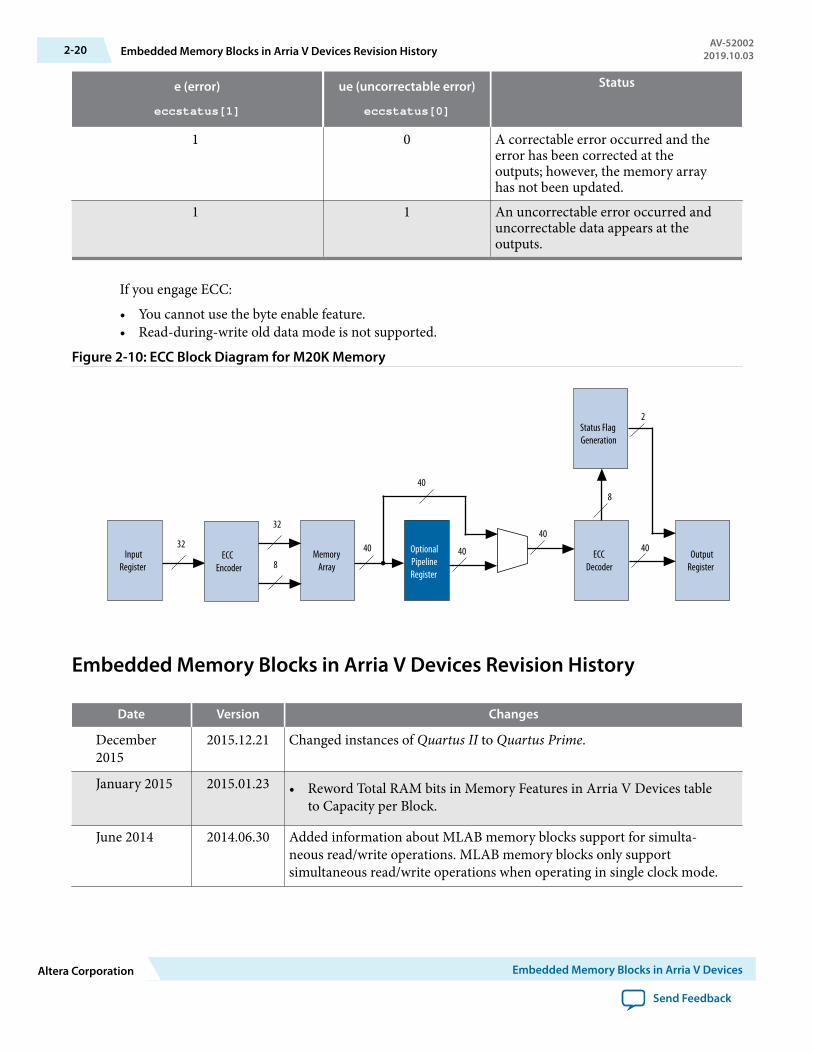
e (error)
eccstatus[1]
ue (uncorrectable error)
eccstatus[0]
Status
1 0 A correctable error occurred and theerror has been corrected at theoutputs; however, the memory arrayhas not been updated.
1 1 An uncorrectable error occurred anduncorrectable data appears at theoutputs.
If you engage ECC:
• You cannot use the byte enable feature.• Read-during-write old data mode is not supported.
Figure 2-10: ECC Block Diagram for M20K Memory
Input Register
32Memory
ArrayECC
Decoder
Status FlagGeneration
OutputRegister
40 40
40
40
ECC Encoder 8
32
OptionalPipelineRegister
40
8
2
Embedded Memory Blocks in Arria V Devices Revision History
Date Version Changes
December2015
2015.12.21 Changed instances of Quartus II to Quartus Prime.
January 2015 2015.01.23 • Reword Total RAM bits in Memory Features in Arria V Devices tableto Capacity per Block.
June 2014 2014.06.30 Added information about MLAB memory blocks support for simulta‐neous read/write operations. MLAB memory blocks only supportsimultaneous read/write operations when operating in single clock mode.
2-20 Embedded Memory Blocks in Arria V Devices Revision HistoryAV-52002
2019.10.03
Altera Corporation Embedded Memory Blocks in Arria V Devices
Send Feedback
Date Version Changes
May 2013 2013.05.06 • Moved all links to the Related Information section of respective topicsfor easy reference.
• Added link to the known document issues in the Knowledge Base.• Corrected the description about the "don't care" output mode for
RAM in mixed-port read-during-write.• Reorganized the structure of the supported memory configurations
topics (single-port and mixed-width dual-port) to improve clarityabout maximum data widths supported for each configuration.
• Added a description to the table listing the maximum embeddedmemory configurations to clarify that the information applies only tothe single port or ROM mode.
• Removed the topic about mixed-width configurations for MLABs andadded a note to clarify that MLABs do not support mixed-widthconfiguration.
November2012
2012.11.19 • Reorganized content and updated template.• Added information for Arria V GZ including M20K memory,
memory features, and memory capacity.• Added and updated memory capacity information from the Arria V
Device Overview for easy reference.• Moved information about supported memory block configurations
into its own table.• Added short descriptions of each clocking mode.• Added topic about the packed mode support.• Added topic about the address clock enable support.• Added topic about ECC support and the ECC truth table.
June 2012 2.0 • Restructured the chapter.• Updated the “Memory Modes”, “Clocking Modes”, and “Design
Considerations” sections.• Updated Table 2–1.• Added the “Parity Bit” and “Byte Enable” sections.• Moved the memory capacity information to the Arria V Device
Overview.
November2011
1.1 • Updated Table 2–1.• Restructured chapter.
May 2011 1.0 Initial release.
AV-520022019.10.03 Embedded Memory Blocks in Arria V Devices Revision History 2-21
Embedded Memory Blocks in Arria V Devices Altera Corporation
Send Feedback

Variable Precision DSP Blocks in Arria V Devices 32019.10.03
AV-52003 Subscribe Send Feedback
This chapter describes how the variable-precision digital signal processing (DSP) blocks in Arria V devicesare optimized to support higher bit precision in high-performance DSP applications.
Related InformationArria V Device Handbook: Known IssuesLists the planned updates to the Arria V Device Handbook chapters.
FeaturesThe Arria V variable precision DSP blocks offer the following features:
• High-performance, power-optimized, and fully registered multiplication operations• 9-bit, 18-bit, 27-bit, and 36-bit(2) word lengths• 18 x 19 and 18 x 25 complex multiplications (2)
• Built-in addition, subtraction, and 64-bit accumulation unit to combine multiplication results• Cascading 19-bit or 27-bit to form the tap-delay line for filtering applications• Cascading 64-bit output bus to propagate output results from one block to the next block without
external logic support• Hard pre-adder supported in 18-bit, 19-bit, and 27-bit mode for symmetric filters• Internal coefficient register bank for filter implementation• 18-bit and 27-bit systolic finite impulse response (FIR) filters with distributed output adder
Related InformationArria V Device OverviewProvides more information about the number of multipliers in each Arria V device.
(2) Only applicable for certain device variant. Refer to Supported Operational Modes in Arria V Devices fordetails.
Intel Corporation. All rights reserved. Intel, the Intel logo, Altera, Arria, Cyclone, Enpirion, MAX, Nios, Quartus and Stratix words and logos are trademarks ofIntel Corporation or its subsidiaries in the U.S. and/or other countries. Intel warrants performance of its FPGA and semiconductor products to currentspecifications in accordance with Intel's standard warranty, but reserves the right to make changes to any products and services at any time without notice.Intel assumes no responsibility or liability arising out of the application or use of any information, product, or service described herein except as expresslyagreed to in writing by Intel. Intel customers are advised to obtain the latest version of device specifications before relying on any published informationand before placing orders for products or services.*Other names and brands may be claimed as the property of others.
ISO9001:2015Registered
www.altera.com101 Innovation Drive, San Jose, CA 95134
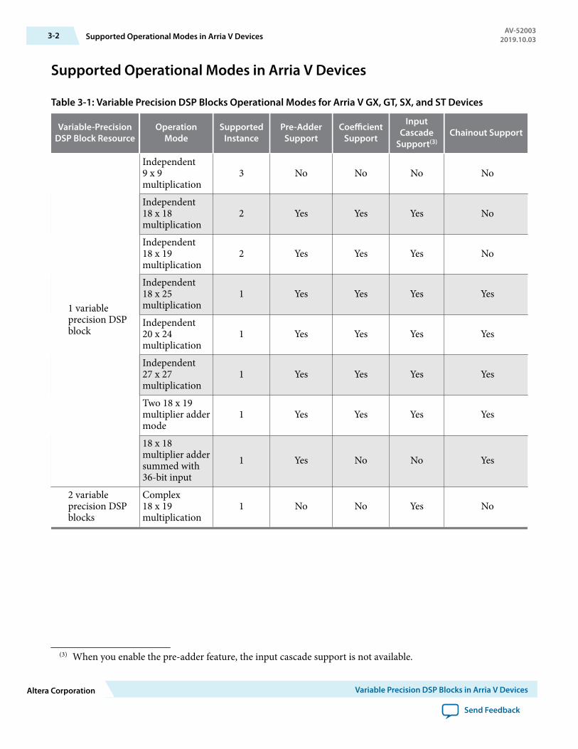
Supported Operational Modes in Arria V Devices
Table 3-1: Variable Precision DSP Blocks Operational Modes for Arria V GX, GT, SX, and ST Devices
Variable-PrecisionDSP Block Resource
OperationMode
SupportedInstance
Pre-AdderSupport
CoefficientSupport
InputCascade
Support(3)Chainout Support
1 variableprecision DSPblock
Independent9 x 9multiplication
3 No No No No
Independent18 x 18multiplication
2 Yes Yes Yes No
Independent18 x 19multiplication
2 Yes Yes Yes No
Independent18 x 25multiplication
1 Yes Yes Yes Yes
Independent20 x 24multiplication
1 Yes Yes Yes Yes
Independent27 x 27multiplication
1 Yes Yes Yes Yes
Two 18 x 19multiplier addermode
1 Yes Yes Yes Yes
18 x 18multiplier addersummed with36-bit input
1 Yes No No Yes
2 variableprecision DSPblocks
Complex18 x 19multiplication
1 No No Yes No
(3) When you enable the pre-adder feature, the input cascade support is not available.
3-2 Supported Operational Modes in Arria V DevicesAV-52003
2019.10.03
Altera Corporation Variable Precision DSP Blocks in Arria V Devices
Send Feedback
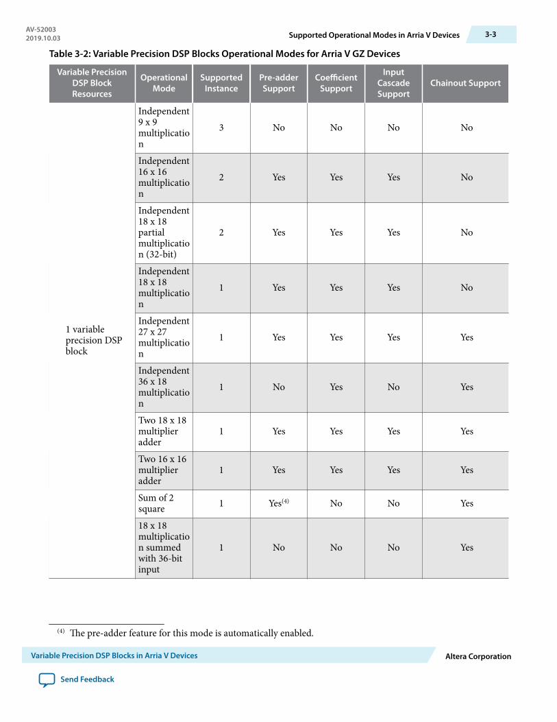
Table 3-2: Variable Precision DSP Blocks Operational Modes for Arria V GZ Devices
Variable PrecisionDSP BlockResources
OperationalMode
SupportedInstance
Pre-adderSupport
CoefficientSupport
InputCascadeSupport
Chainout Support
1 variableprecision DSPblock
Independent9 x 9multiplication
3 No No No No
Independent16 x 16multiplication
2 Yes Yes Yes No
Independent18 x 18partialmultiplication (32-bit)
2 Yes Yes Yes No
Independent18 x 18multiplication
1 Yes Yes Yes No
Independent27 x 27multiplication
1 Yes Yes Yes Yes
Independent36 x 18multiplication
1 No Yes No Yes
Two 18 x 18multiplieradder
1 Yes Yes Yes Yes
Two 16 x 16multiplieradder
1 Yes Yes Yes Yes
Sum of 2square 1 Yes(4) No No Yes
18 x 18multiplication summedwith 36-bitinput
1 No No No Yes
(4) The pre-adder feature for this mode is automatically enabled.
AV-520032019.10.03 Supported Operational Modes in Arria V Devices 3-3
Variable Precision DSP Blocks in Arria V Devices Altera Corporation
Send Feedback

Variable PrecisionDSP BlockResources
OperationalMode
SupportedInstance
Pre-adderSupport
CoefficientSupport
InputCascadeSupport
Chainout Support
2 variableprecision DSPblocks
Independent18 x 18multiplication
3 No No No No
Independent36 x 36multiplication
1 No No No No
Complex18 x 18multiplication
1 Yes Yes Yes Yes
Four 18 x 18multiplieradder
1 Yes Yes Yes No
Two 27 x 27multiplieradder
1 Yes Yes Yes No
Two 18 x 36multiplieradder
1 No Yes No No
3 variableprecision DSPblocks
Complex18 x 25multiplication
1 Yes(4) No No No
4 variableprecision DSPblocks
Complex27 x 27multiplication
1 Yes Yes Yes No
Resources
Table 3-3: Number of Multipliers in Arria V Devices
The table lists the variable-precision DSP resources by bit precision for each Arria V device.
3-4 ResourcesAV-52003
2019.10.03
Altera Corporation Variable Precision DSP Blocks in Arria V Devices
Send Feedback
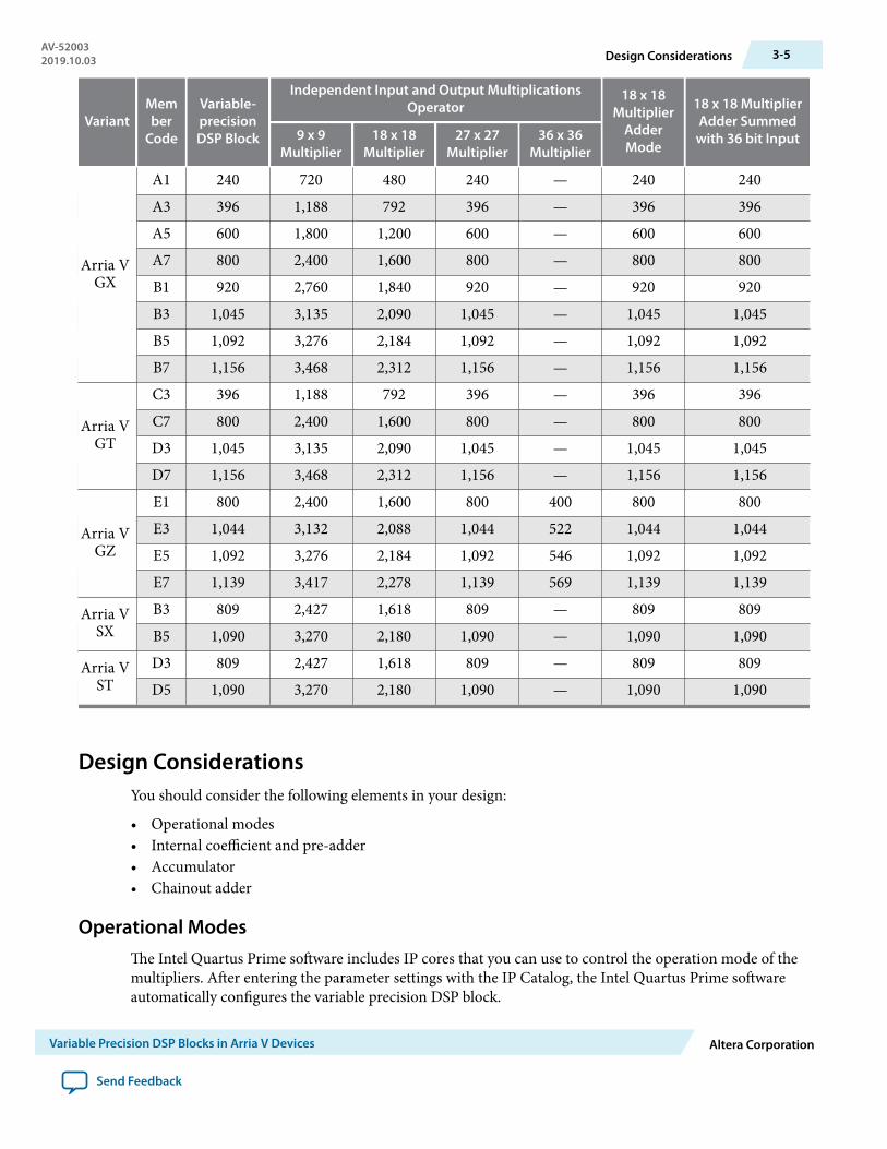
VariantMember
Code
Variable-precisionDSP Block
Independent Input and Output MultiplicationsOperator
18 x 18Multiplier
AdderMode
18 x 18 MultiplierAdder Summed
with 36 bit Input9 x 9Multiplier
18 x 18Multiplier
27 x 27Multiplier
36 x 36Multiplier
Arria VGX
A1 240 720 480 240 — 240 240A3 396 1,188 792 396 — 396 396A5 600 1,800 1,200 600 — 600 600A7 800 2,400 1,600 800 — 800 800B1 920 2,760 1,840 920 — 920 920B3 1,045 3,135 2,090 1,045 — 1,045 1,045B5 1,092 3,276 2,184 1,092 — 1,092 1,092B7 1,156 3,468 2,312 1,156 — 1,156 1,156
Arria VGT
C3 396 1,188 792 396 — 396 396C7 800 2,400 1,600 800 — 800 800D3 1,045 3,135 2,090 1,045 — 1,045 1,045D7 1,156 3,468 2,312 1,156 — 1,156 1,156
Arria VGZ
E1 800 2,400 1,600 800 400 800 800E3 1,044 3,132 2,088 1,044 522 1,044 1,044E5 1,092 3,276 2,184 1,092 546 1,092 1,092E7 1,139 3,417 2,278 1,139 569 1,139 1,139
Arria VSX
B3 809 2,427 1,618 809 — 809 809B5 1,090 3,270 2,180 1,090 — 1,090 1,090
Arria VST
D3 809 2,427 1,618 809 — 809 809D5 1,090 3,270 2,180 1,090 — 1,090 1,090
Design ConsiderationsYou should consider the following elements in your design:
• Operational modes• Internal coefficient and pre-adder• Accumulator• Chainout adder
Operational ModesThe Intel Quartus Prime software includes IP cores that you can use to control the operation mode of themultipliers. After entering the parameter settings with the IP Catalog, the Intel Quartus Prime softwareautomatically configures the variable precision DSP block.
AV-520032019.10.03 Design Considerations 3-5
Variable Precision DSP Blocks in Arria V Devices Altera Corporation
Send Feedback

Altera provides two methods for implementing various modes of the Arria V variable precision DSP blockin a design—using the Intel Quartus Prime DSP IP cores and HDL inferring.
The following Intel Quartus Prime IP cores are supported for the Arria V variable precision DSP blocksimplementation:
• LPM_MULT• ALTERA_MULT_ADD• ALTMULT_COMPLEX• ALTMEMMULT
Related Information
• Introduction to Altera IP Cores• Integer Arithmetic IP Cores User Guide• Floating-Point IP Cores User Guide• Quartus II Software Help
Internal Coefficient and Pre-AdderTo use the pre-adder feature, all input data and multipliers must have the same clock setting.
The input cascade support is not available when you enable the pre-adder feature.
Table 3-4: Internal Coefficient and Pre-Adder Features in Arria V Devices
Mode Arria V GX, GT, SX, and ST Arria V GZ
18-bit The coefficient feature and pre-adder featurecan be used independently.
The coefficient feature must be enabledwhen the pre-adder feature is enabled.
27-bit The coefficient feature and pre-adder featurecan be used independently.
The coefficient feature and pre-adderfeature can be used independently.
With pre-adder enabled:
• If the multiplicand input comes fromdynamic input due to widthlimitation in the input registers—theinput data width is restricted to22 bits.
• If the multiplicand input comes fromthe internal coefficients—the datawidth of the multiplicand is 27 bits.
Note: When you enable the pre-adder feature, all input data must have the same clock setting.
AccumulatorThe accumulator in the Arria V GX, GT, SX, and ST devices supports double accumulation by enablingthe 64-bit double accumulation registers located between the output register bank and the accumulator.
3-6 Internal Coefficient and Pre-AdderAV-52003
2019.10.03
Altera Corporation Variable Precision DSP Blocks in Arria V Devices
Send Feedback

The double accumulation registers are set statically in the programming file.
The accumulator in the Arria V GZ devices does not support double accumulation. The accumulatorfeature is not available in multi-block modes.
Chainout AdderYou can use the output chaining path to add results from other DSP blocks.
Block ArchitectureThe Arria V variable precision DSP block consists of the following elements:
• Input register bank• Pre-adder• Internal coefficient• Multipliers• Adder• Accumulator and chainout adder• Systolic registers• Double accumulation register• Output register bank
If the variable precision DSP block is not configured in systolic FIR mode, both systolic registers arebypassed.
AV-520032019.10.03 Chainout Adder 3-7
Variable Precision DSP Blocks in Arria V Devices Altera Corporation
Send Feedback

Figure 3-1: Variable Precision DSP Block Architecture in 18 x 19 Mode for Arria V GX, GT, SX, and ST Devices
Inpu
t Reg
ister
Bank
scanin
scanout
LOADCONST
ACCUMULATE
NEGATE
dataa_y0[18..0]
dataa_z0[17..0]
dataa_x0[17..0]
COEFSELA[2..0]
datab_y1[18..0]
datab_z1[17..0]
datab_x1[17..0]
COEFSELB[2..0]
SUB_COMPLEX
+/-
Pre-Adder
+/-
Pre-Adder
+/-
InternalCoefficient
InternalCoefficient
Multiplier
Adder
+/- +/-
Systolic Registers
(1)
Systolic Register (1)
Chainout adder/accumulator
+
Outp
ut Re
giste
r Ban
k
Constant
Double Accumulation
Register
chainin[63..0]
chainout[63..0]
Result[73..0]
Multiplier
x
x
CLK[2..0]
ENA[2..0]
ACLR[1..0]
Note:1. When enabled, systolic registers are clocked with the same clock source as the output register bank.
3-8 Block ArchitectureAV-52003
2019.10.03
Altera Corporation Variable Precision DSP Blocks in Arria V Devices
Send Feedback

Figure 3-2: Variable Precision DSP Block Architecture in 27 x 27 Mode for Arria V GX, GT, SX, and ST Devices
+
Constant
64
DoubleAccumulation
Register
Result[63..0]
chainout[63..0]
InternalCoefficients
+/-
LOADCONST
ACCUMULATE
NEG
dataa_y0[26..0]dataa_z0[25..0]
dataa_x0[26..0]
COEFSELA[2..0]
Multiplierx
chainin[63..0]
OutputRegister
Bank
Chainout Adder/Accumulator
InputRegister
Bank
Pre-Adder+/-
AV-520032019.10.03 Block Architecture 3-9
Variable Precision DSP Blocks in Arria V Devices Altera Corporation
Send Feedback
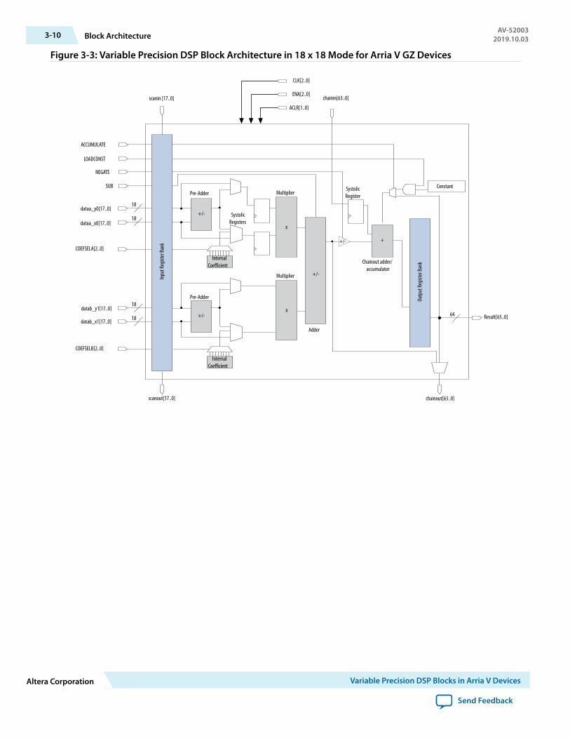
Figure 3-3: Variable Precision DSP Block Architecture in 18 x 18 Mode for Arria V GZ Devices
Outp
ut Re
giste
r Ban
k
COEFSELA[2..0]
COEFSELB[2..0]
+/-
Pre-Adder
+/-
Pre-Adder
+/-
InternalCoefficient
InternalCoefficient
Multiplier
Multiplier
Adder
+/-
Systolic Registers
Systolic Register
Chainout adder/accumulator
+
chainin[63..0]
chainout[63..0]
Result[65..0]
x
x
dataa_y0[17..0]
dataa_x0[17..0]
datab_y1[17..0]
datab_x1[17..0]
18
18
18
1864
ACCUMULATE
LOADCONST
NEGATE
SUB Constant
CLK[2..0]
ENA[2..0]
ACLR[1..0]
scanin [17..0]
Inpu
t Reg
ister
Bank
scanout[17..0]
+/-
3-10 Block ArchitectureAV-52003
2019.10.03
Altera Corporation Variable Precision DSP Blocks in Arria V Devices
Send Feedback
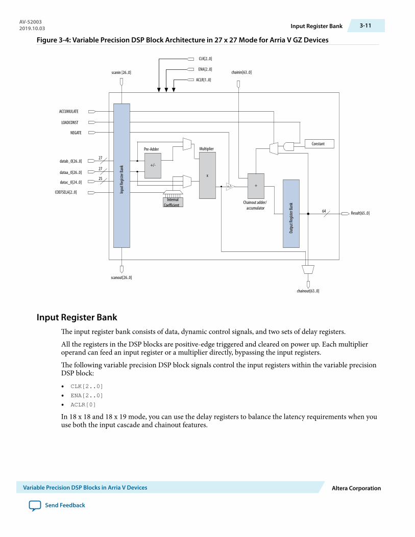
Figure 3-4: Variable Precision DSP Block Architecture in 27 x 27 Mode for Arria V GZ Devices
Outp
ut Re
giste
r Ban
k
COEFSELA[2..0]
Pre-Adder
+/-
InternalCoefficient
Multiplier
Chainout adder/accumulator
+
chainin[63..0]
chainout[63..0]
Result[65..0]
x
datab_0[26..0]
dataa_0[26..0]
27
27
datac_0[24..0]25
64
ACCUMULATE
LOADCONST
NEGATE
Constant
CLK[2..0]
ENA[2..0]
ACLR[1..0]
scanin [26..0]
Inpu
t Reg
ister
Bank
scanout[26..0]
+/-
Input Register BankThe input register bank consists of data, dynamic control signals, and two sets of delay registers.
All the registers in the DSP blocks are positive-edge triggered and cleared on power up. Each multiplieroperand can feed an input register or a multiplier directly, bypassing the input registers.
The following variable precision DSP block signals control the input registers within the variable precisionDSP block:
• CLK[2..0]
• ENA[2..0]
• ACLR[0]
In 18 x 18 and 18 x 19 mode, you can use the delay registers to balance the latency requirements when youuse both the input cascade and chainout features.
AV-520032019.10.03 Input Register Bank 3-11
Variable Precision DSP Blocks in Arria V Devices Altera Corporation
Send Feedback
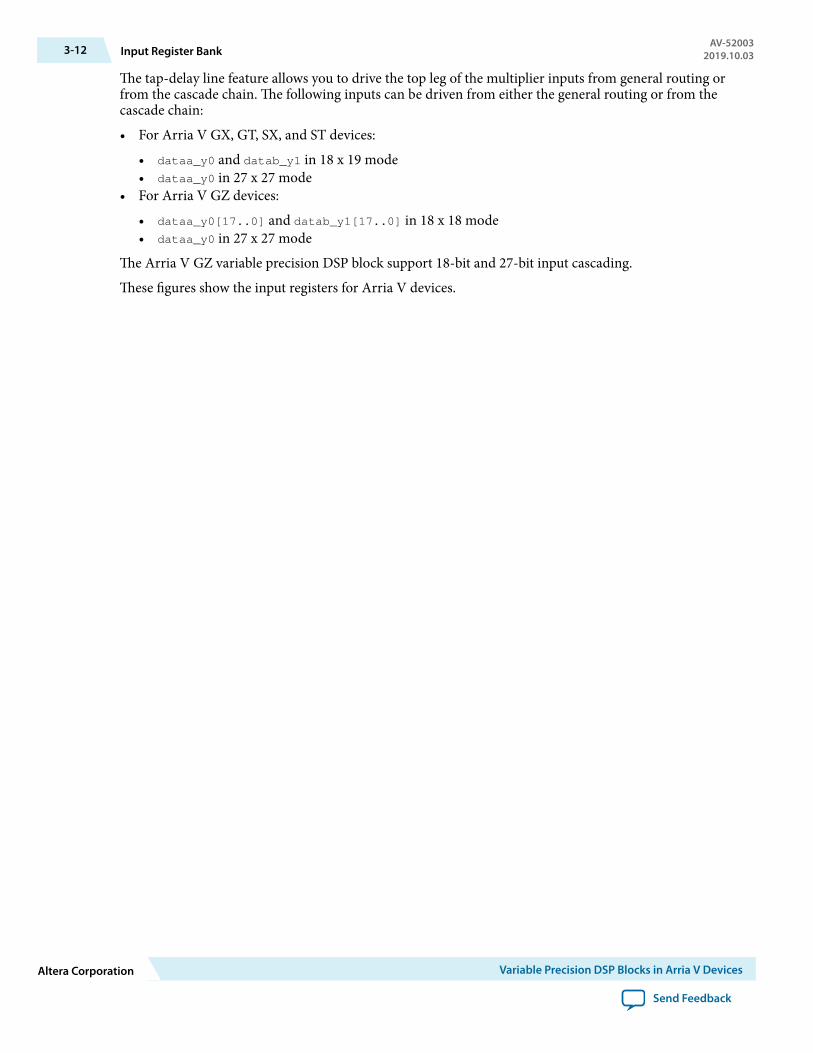
The tap-delay line feature allows you to drive the top leg of the multiplier inputs from general routing orfrom the cascade chain. The following inputs can be driven from either the general routing or from thecascade chain:
• For Arria V GX, GT, SX, and ST devices:
• dataa_y0 and datab_y1 in 18 x 19 mode• dataa_y0 in 27 x 27 mode
• For Arria V GZ devices:
• dataa_y0[17..0] and datab_y1[17..0] in 18 x 18 mode• dataa_y0 in 27 x 27 mode
The Arria V GZ variable precision DSP block support 18-bit and 27-bit input cascading.
These figures show the input registers for Arria V devices.
3-12 Input Register BankAV-52003
2019.10.03
Altera Corporation Variable Precision DSP Blocks in Arria V Devices
Send Feedback
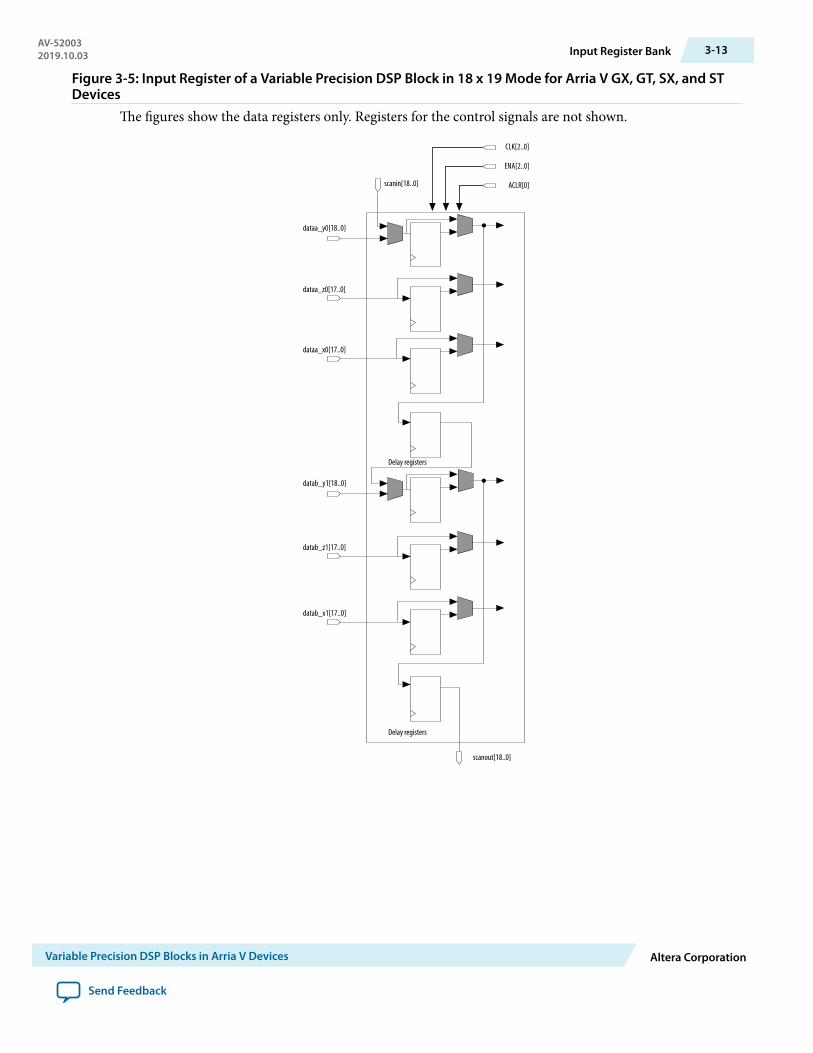
Figure 3-5: Input Register of a Variable Precision DSP Block in 18 x 19 Mode for Arria V GX, GT, SX, and STDevices
The figures show the data registers only. Registers for the control signals are not shown.
dataa_y0[18..0]
dataa_z0[17..0]
dataa_x0[17..0]
datab_y1[18..0]
Delay registers
datab_z1[17..0]
datab_x1[17..0]
Delay registers
scanin[18..0]
scanout[18..0]
CLK[2..0]
ENA[2..0]
ACLR[0]
AV-520032019.10.03 Input Register Bank 3-13
Variable Precision DSP Blocks in Arria V Devices Altera Corporation
Send Feedback
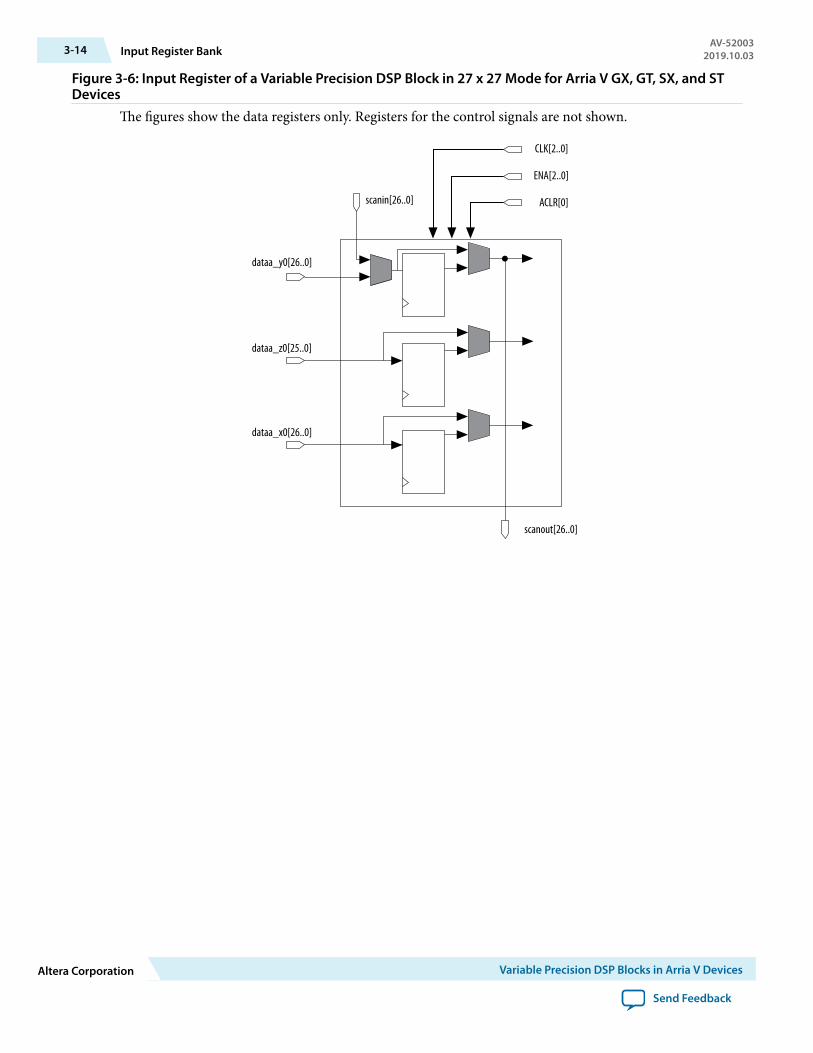
Figure 3-6: Input Register of a Variable Precision DSP Block in 27 x 27 Mode for Arria V GX, GT, SX, and STDevices
The figures show the data registers only. Registers for the control signals are not shown.
dataa_y0[26..0]
dataa_z0[25..0]
dataa_x0[26..0]
scanin[26..0]
CLK[2..0]
ENA[2..0]
ACLR[0]
scanout[26..0]
3-14 Input Register BankAV-52003
2019.10.03
Altera Corporation Variable Precision DSP Blocks in Arria V Devices
Send Feedback

Figure 3-7: Input Register of a Variable Precision DSP Block in 18 x 18 Mode for Arria V GZ DevicesThe figures show the data registers only. Registers for the control signals are not shown.
dataa_y0[17..0]
dataa_x0[17..0]
datab_y1[17..0]
Delay registers
datab_x1[17..0]
Delay registers
scanin[17..0]
scanout[17..0]
CLK[2..0]
ENA[2..0]
ACLR[0]
AV-520032019.10.03 Input Register Bank 3-15
Variable Precision DSP Blocks in Arria V Devices Altera Corporation
Send Feedback

Figure 3-8: Input Register of a Variable Precision DSP Block in 27 x 27 Mode for Arria V GZ DevicesThe figures show the data registers only. Registers for the control signals are not shown.
dataa_y0[26..0]
dataa_x0[26..0]
dataa_z0[24..0]
scanin[26..0]
CLK[2..0]
ENA[2..0]
ACLR[0]
scanout[26..0]
Pre-Adder
Arria V GX, GT, SX, and ST Devices
Each variable precision DSP block has two 19-bit pre-adders. You can configure these pre-adders in thefollowing configurations:
• Two independent 19-bit pre-adders• One 27-bit pre-adder
The pre-adder supports both addition and subtraction in the following input configurations:
• 18-bit (signed) addition or subtraction for 18 x 19 mode• 17-bit (unsigned) addition or subtraction for 18 x 19 mode• 26-bit addition or subtraction for 27 x 27 mode
Arria V GZ Devices
Each variable precision DSP block has two 18-bit pre-adders. You can configure these pre-adders in thefollowing configurations:
• Two independent 18-bit adders• One 26-bit adder
3-16 Pre-AdderAV-52003
2019.10.03
Altera Corporation Variable Precision DSP Blocks in Arria V Devices
Send Feedback
The pre-adder supports both addition and subtraction in the following input configurations:
• 17-bit addition or subtraction for 18-bit applications• 25-bit addition or subtraction for 27-bit applications
Internal CoefficientThe Arria V variable precision DSP block has the flexibility of selecting the multiplicand from either thedynamic input or the internal coefficient.
The internal coefficient can support up to eight constant coefficients for the multiplicands in 18-bit and27-bit modes. When you enable the internal coefficient feature, COEFSELA/COEFSELB are used to controlthe selection of the coefficient multiplexer.
MultipliersA single variable precision DSP block can perform many multiplications in parallel, depending on the datawidth of the multiplier.
There are two multipliers per variable precision DSP block. You can configure these two multipliers inseveral operational modes.
For Arria V GX, GT, SX, and ST devices:
• One 27 x 27 multiplier• Two 18 (signed)/(unsigned) x 19 (signed) multipliers• Three 9 x 9 multipliers
For Arria V GZ devices:
• One 27 x 27 multiplier• Two individual 16 x 16 multipliers• Two individual 18 x 18 partial multipliers, with only 32-bit LSB multiplication result for each multipli‐
cation• One individual 18 x 18 multiplier, with full 36-bit multiplication result• One individual 27 x 27 multiplier• One individual 36 x 18 multiplier• There individual 9 x 9 multipliers
For Arria V GZ devices, you can use two adjacent DSP blocks to construct an individual 36-bit multiplier.
Related InformationOperational Mode Descriptions on page 3-19Provides more information about the operational modes of the multipliers.
AdderYou can use the adder in various sizes, depending on the operational mode:
• One 64-bit adder with the 64-bit accumulator• Two 18 x 19 modes—the adder is divided into two 37-bit adders to produce the full 37-bit result of
each independent 18 x 19 multiplication• Three 9 x 9 modes—you can use the adder as three 18-bit adders to produce three 9 x 9 multiplication
results independently
AV-520032019.10.03 Internal Coefficient 3-17
Variable Precision DSP Blocks in Arria V Devices Altera Corporation
Send Feedback

Accumulator and Chainout AdderThe Arria V variable precision DSP block supports a 64-bit accumulator and a 64-bit adder.
For Arria V GX, GT, SX, and ST devices, the accumulator and chainout adder features are not supportedin two independent 18 x 19 modes and three independent 9 x 9 modes.
For Arria V GZ devices, you can use the 64-bit adder as full adder.
The following signals can dynamically control the function of the accumulator:
• NEGATE
• LOADCONST
• ACCUMULATE
Table 3-5: Accumulator Functions and Dynamic Control Signals
This table lists the dynamic signals settings and description for each function. In this table, X denotes a"don't care" value.
Function Description NEGATE LOADCONST ACCUMULATE
Zeroing Disables theaccumulator. 0 0 0
Preload
Loads an initial valueto the accumulator.Only one bit of the64-bit preload valuecan be “1”. It can beused as rounding theDSP result to anyposition of the 64-bitresult.
0 1 0
AccumulationAdds the currentresult to the previousaccumulate result.
0 X 1
Decimation
This function takesthe current result,converts it into two’scomplement, andadds it to theprevious result.
1 X 1
Systolic RegistersThere are two systolic registers per variable precision DSP block. If the variable precision DSP block is notconfigured in systolic FIR mode, both systolic registers are bypassed.
The first set of systolic registers consists of the following registers:
• 18-bit and 19-bit registers that are used to register the 18-bit and 19-bit inputs of the upper multiplierrespectively for Arria V GX, GT, SX, and ST devices
• 18-bit registers that are used to register the 18-bit inputs of the upper multiplier for Arria V GZ devices
3-18 Accumulator and Chainout AdderAV-52003
2019.10.03
Altera Corporation Variable Precision DSP Blocks in Arria V Devices
Send Feedback

The second set of systolic registers are used to delay the chainout output to the next variable precision DSPblock.
You must clock all the systolic registers with the same clock source as the output register bank.
Double Accumulation RegisterThe double accumulation register is an extra register in the feedback path of the accumulator. Enabling thedouble accumulation register will cause an extra clock cycle delay in the feedback path of the accumulator.
This register has the same CLK, ENA, and ACLR settings as the output register bank.
By enabling this register, you can have two accumulator channels using the same number of variableprecision DSP block.
Double accumulation register is not available in Arria V GZ devices.
Output Register BankThe positive edge of the clock signal triggers the 64-bit bypassable output register bank and is cleared afterpower up.
The following variable precision DSP block signals control the output register per variable precision DSPblock:
• CLK[2..0]
• ENA[2..0]
• ACLR[1]
Operational Mode DescriptionsThis section describes how you can configure an Arria V variable precision DSP block to efficientlysupport the following operational modes:
• Independent Multiplier Mode• Independent Complex Multiplier Mode• Multiplier Adder Sum Mode• Sum of Square Mode (Arria V GZ only)• 18 x 18 Multiplication Summed with 36-Bit Input Mode• Systolic FIR Mode
Independent Multiplier ModeIn independent input and output multiplier mode, the variable precision DSP blocks perform individualmultiplication operations for general purpose multipliers.
Table 3-6: Variable Precision DSP Block Independent Multiplier Mode Configurations for Arria V Devices
Configuration Multipliers per block Device Variant Support
9 x 9 3 All16 x 16 1 Arria V GZ
AV-520032019.10.03 Double Accumulation Register 3-19
Variable Precision DSP Blocks in Arria V Devices Altera Corporation
Send Feedback
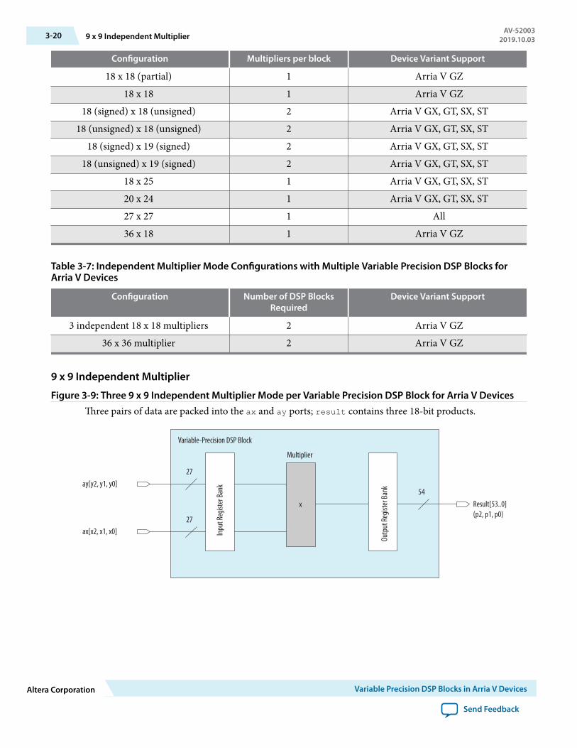
Configuration Multipliers per block Device Variant Support
18 x 18 (partial) 1 Arria V GZ18 x 18 1 Arria V GZ
18 (signed) x 18 (unsigned) 2 Arria V GX, GT, SX, ST18 (unsigned) x 18 (unsigned) 2 Arria V GX, GT, SX, ST
18 (signed) x 19 (signed) 2 Arria V GX, GT, SX, ST18 (unsigned) x 19 (signed) 2 Arria V GX, GT, SX, ST
18 x 25 1 Arria V GX, GT, SX, ST20 x 24 1 Arria V GX, GT, SX, ST27 x 27 1 All36 x 18 1 Arria V GZ
Table 3-7: Independent Multiplier Mode Configurations with Multiple Variable Precision DSP Blocks forArria V Devices
Configuration Number of DSP BlocksRequired
Device Variant Support
3 independent 18 x 18 multipliers 2 Arria V GZ36 x 36 multiplier 2 Arria V GZ
9 x 9 Independent Multiplier
Figure 3-9: Three 9 x 9 Independent Multiplier Mode per Variable Precision DSP Block for Arria V DevicesThree pairs of data are packed into the ax and ay ports; result contains three 18-bit products.
Inpu
t Reg
ister
Bank
Multiplier
x Result[53..0](p2, p1, p0)
ay[y2, y1, y0]
ax[x2, x1, x0]
27
27
54
Variable-Precision DSP Block
Outp
ut Re
giste
r Ban
k
3-20 9 x 9 Independent MultiplierAV-52003
2019.10.03
Altera Corporation Variable Precision DSP Blocks in Arria V Devices
Send Feedback
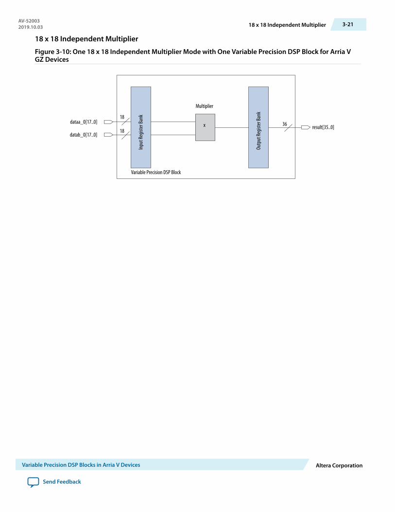
18 x 18 Independent Multiplier
Figure 3-10: One 18 x 18 Independent Multiplier Mode with One Variable Precision DSP Block for Arria VGZ Devices
result[35..0]
Outp
ut Re
giste
r Ban
k
dataa_0[17..0]
datab_0[17..0]
Multiplier
Variable Precision DSP Block
x 3618
18
Inpu
t Reg
ister
Bank
AV-520032019.10.03 18 x 18 Independent Multiplier 3-21
Variable Precision DSP Blocks in Arria V Devices Altera Corporation
Send Feedback

Figure 3-11: Three 18 x 18 Independent Multiplier Mode with Two Variable Precision DSP Blocks for Arria VGZ Devices
datab_0[17..0]
dataa_0[17..0]
dataa_2[17..0]
dataa_2[17..0]
datab_2[17..0]
datab_2[17..0]
datab_1[17..0]
dataa_1[17..0]
Variable Precision DSP Block 1
Variable Precision DSP Block 2
result_0[35..0]
result_1[35..0]
result_2[17..0]
result_2[35..18]
Multiplier
Inpu
t Reg
ister
Bank
Outp
ut Re
giste
r Ban
k
x
Multiplier
x
x
x
Outp
ut Re
giste
r Ban
k
18
36
18
18
36
18
18
18
18
18
18
18
Inpu
t Reg
ister
Bank
Multiplier
Multiplier
3-22 18 x 18 Independent MultiplierAV-52003
2019.10.03
Altera Corporation Variable Precision DSP Blocks in Arria V Devices
Send Feedback

18 x 18 or 18 x 19 Independent Multiplier
Figure 3-12: Two 18 x 18 or 18 x 19 Independent Multiplier Mode per Variable Precision DSP Block forArria V GX, GT, SX, and ST Devices
In this figure, the variables are defined as follows:
• n = 19 and m = 37 for 18 x 19 mode• n = 18 and m = 36 for 18 x 18 mode
[(m-1)..0]
Multiplier
x
Multiplier
x
Inpu
t Reg
ister
Bank
data_b1[(n-1)..0]
data_a1[17..0]
n
18
Variable-Precision DSP Block
data_b0[(n-1)..0]
data_a0[17..0]
n
18
m
[(m-1)..0]m
Outp
ut Re
giste
r Ban
k
AV-520032019.10.03 18 x 18 or 18 x 19 Independent Multiplier 3-23
Variable Precision DSP Blocks in Arria V Devices Altera Corporation
Send Feedback
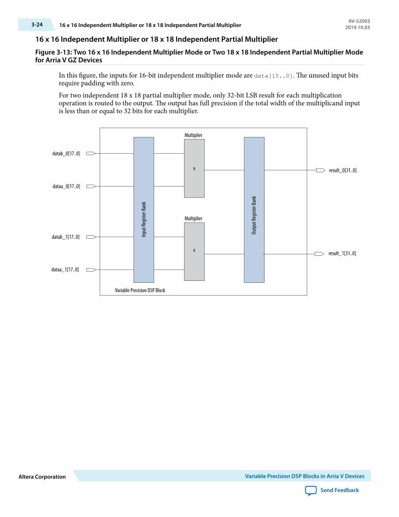
16 x 16 Independent Multiplier or 18 x 18 Independent Partial Multiplier
Figure 3-13: Two 16 x 16 Independent Multiplier Mode or Two 18 x 18 Independent Partial Multiplier Modefor Arria V GZ Devices
In this figure, the inputs for 16-bit independent multiplier mode are data[15..0]. The unused input bitsrequire padding with zero.
For two independent 18 x 18 partial multiplier mode, only 32-bit LSB result for each multiplicationoperation is routed to the output. The output has full precision if the total width of the multiplicand inputis less than or equal to 32 bits for each multiplier.
datab_0[17..0]
dataa_0[17..0]
dataa_1[17..0]
datab_1[17..0] Inpu
t Reg
ister
Bank
Outp
ut Re
giste
r Ban
k
Multiplier
x
x
Multiplier
Variable Precision DSP Block
result_0[31..0]
result_1[31..0]
3-24 16 x 16 Independent Multiplier or 18 x 18 Independent Partial MultiplierAV-52003
2019.10.03
Altera Corporation Variable Precision DSP Blocks in Arria V Devices
Send Feedback
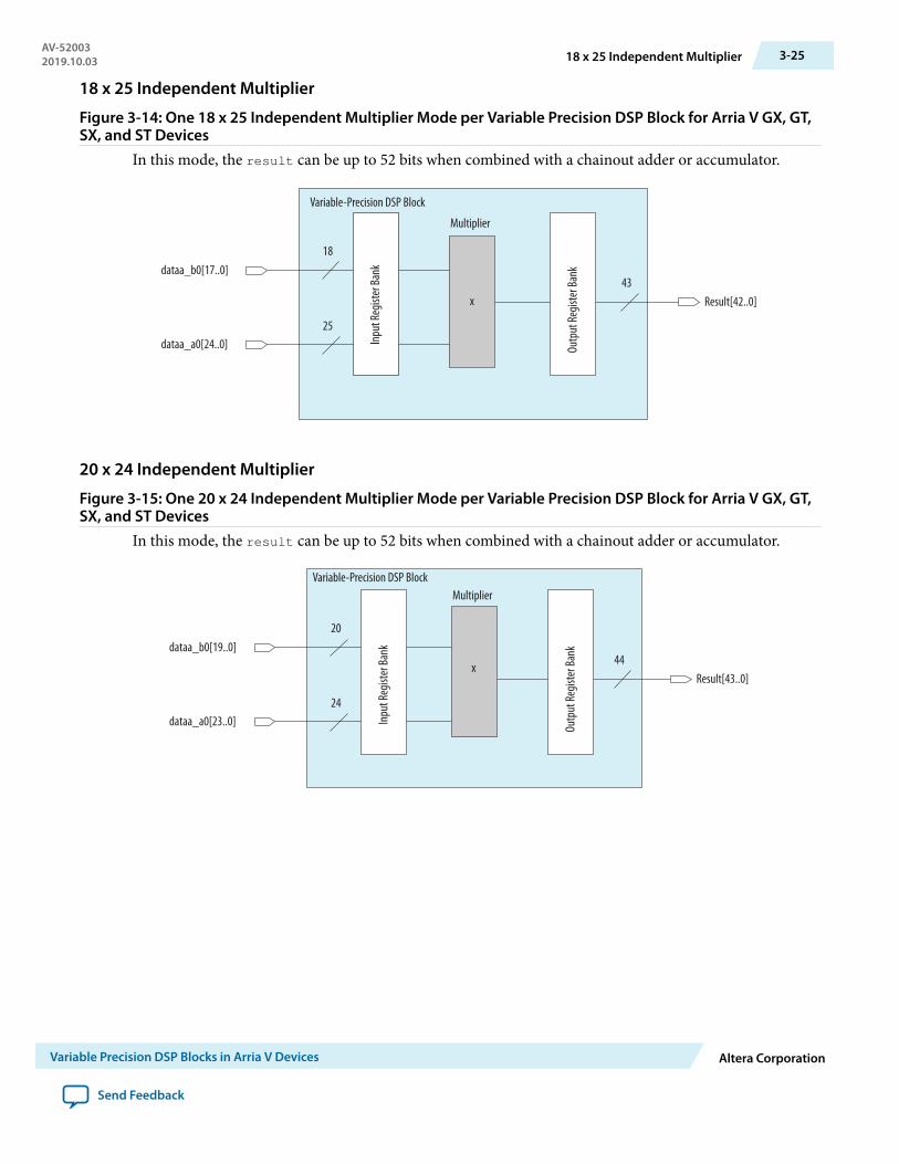
18 x 25 Independent Multiplier
Figure 3-14: One 18 x 25 Independent Multiplier Mode per Variable Precision DSP Block for Arria V GX, GT,SX, and ST Devices
In this mode, the result can be up to 52 bits when combined with a chainout adder or accumulator.
Inpu
t Reg
ister
Bank
Multiplier
Result[42..0]
dataa_b0[17..0]
dataa_a0[24..0]
18
25
43
Variable-Precision DSP Block
Outp
ut Re
giste
r Ban
k
x
20 x 24 Independent Multiplier
Figure 3-15: One 20 x 24 Independent Multiplier Mode per Variable Precision DSP Block for Arria V GX, GT,SX, and ST Devices
In this mode, the result can be up to 52 bits when combined with a chainout adder or accumulator.
Inpu
t Reg
ister
Bank
Multiplier
xResult[43..0]
dataa_b0[19..0]
dataa_a0[23..0]
20
24
44
Variable-Precision DSP BlockOu
tput
Regis
ter B
ank
AV-520032019.10.03 18 x 25 Independent Multiplier 3-25
Variable Precision DSP Blocks in Arria V Devices Altera Corporation
Send Feedback

27 x 27 Independent Multiplier
Figure 3-16: One 27 x 27 Independent Multiplier Mode per Variable Precision DSP Block for Arria V DevicesIn this mode, the result can be up to 64 bits when combined with a chainout adder or accumulator.
Inpu
t Reg
ister
Bank
Multiplier
x Result[53..0]
dataa_b0[26..0]
dataa_a0[26..0]
27
27
54
Variable-Precision DSP Block
Outp
ut Re
giste
r Ban
k
36 x 18 Independent Multiplier
Figure 3-17: One 36 x 18 Independent Multiplier Mode for Arria V GZ Devices
Outp
ut Re
giste
r Ban
k
dataa_0[35..18]datab_0[17..0]
datab_0[17..0]
dataa_0[17..0]
result[53..0]
Multiplier
x
Multiplier
Variable Precision DSP Block
+
x
Inpu
t Reg
ister
Bank
18
18
1818
54
36-Bit Independent Multiplier
You can efficiently construct an individual 36-bit multiplier with two adjacent variable precision DSPblocks. The 36 x 36 multiplication consists of four 18 x 18 multipliers.
3-26 27 x 27 Independent MultiplierAV-52003
2019.10.03
Altera Corporation Variable Precision DSP Blocks in Arria V Devices
Send Feedback
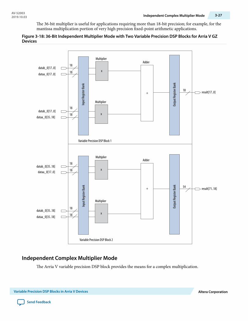
The 36-bit multiplier is useful for applications requiring more than 18-bit precision; for example, for themantissa multiplication portion of very high precision fixed-point arithmetic applications.
Figure 3-18: 36-Bit Independent Multiplier Mode with Two Variable Precision DSP Blocks for Arria V GZDevices
datab_0[17..0]
dataa_0[17..0]
dataa_0[35..18]
datab_0[17..0]
datab_0[35..18]
dataa_0[17..0]
datab_0[35..18]
dataa_0[35..18]
Variable Precision DSP Block 1
Variable Precision DSP Block 2
result[17..0]
result[71..18]
18
18
18
18
18
54
18
18
18
18 x
x
x
x
Multiplier
x
Multiplier
Multiplier
Multiplier
Adder
Adder
+
+
Inpu
t Reg
ister
Bank
Inpu
t Reg
ister
Bank
Outp
ut Re
giste
r Ban
kOu
tput
Regis
ter B
ank
Independent Complex Multiplier ModeThe Arria V variable precision DSP block provides the means for a complex multiplication.
AV-520032019.10.03 Independent Complex Multiplier Mode 3-27
Variable Precision DSP Blocks in Arria V Devices Altera Corporation
Send Feedback
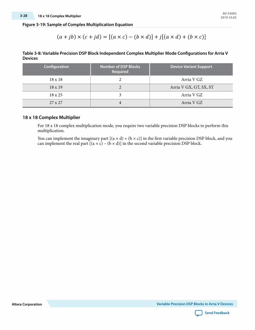
Figure 3-19: Sample of Complex Multiplication Equation
Table 3-8: Variable Precision DSP Block Independent Complex Multiplier Mode Configurations for Arria VDevices
Configuration Number of DSP BlocksRequired
Device Variant Support
18 x 18 2 Arria V GZ18 x 19 2 Arria V GX, GT, SX, ST18 x 25 3 Arria V GZ27 x 27 4 Arria V GZ
18 x 18 Complex Multiplier
For 18 x 18 complex multiplication mode, you require two variable precision DSP blocks to perform thismultiplication.
You can implement the imaginary part [(a × d) + (b × c)] in the first variable precision DSP block, and youcan implement the real part [(a × c) – (b × d)] in the second variable precision DSP block.
3-28 18 x 18 Complex MultiplierAV-52003
2019.10.03
Altera Corporation Variable Precision DSP Blocks in Arria V Devices
Send Feedback
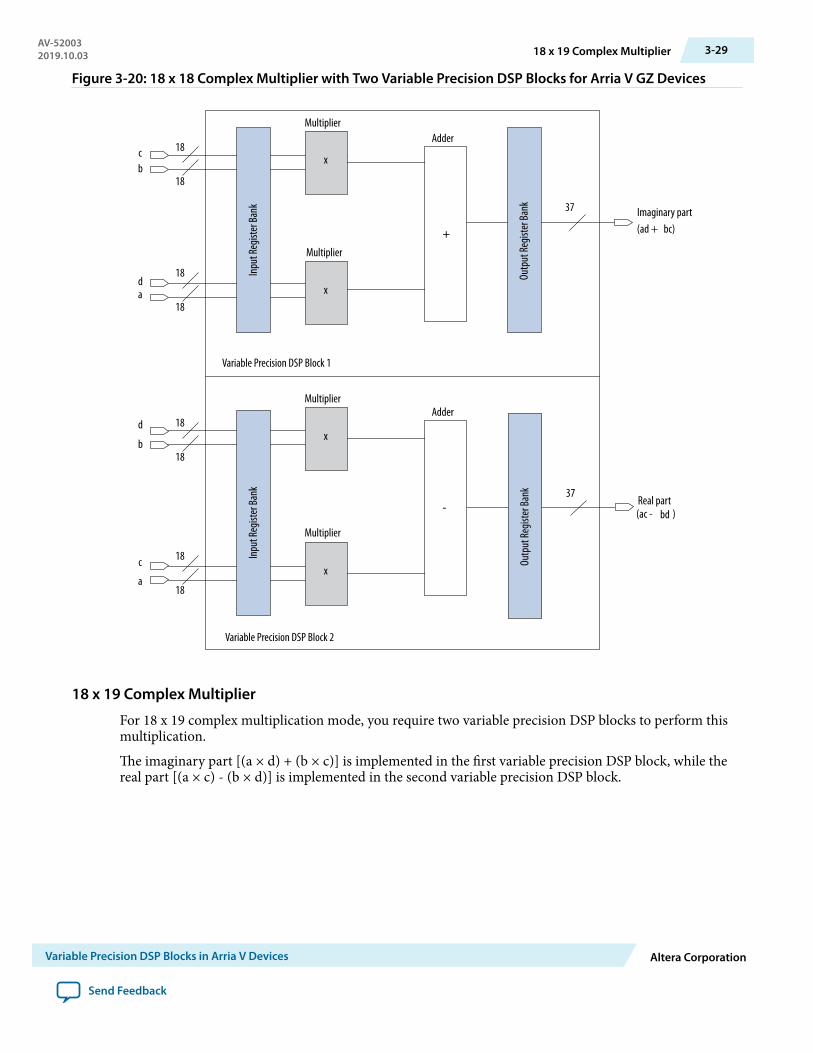
Figure 3-20: 18 x 18 Complex Multiplier with Two Variable Precision DSP Blocks for Arria V GZ Devices
37
37
cb
a
b
d
d
c
a
Variable Precision DSP Block 1
Variable Precision DSP Block 2
18
18
18
18
18
18
18
18
Outp
ut Re
giste
r Ban
kOu
tput
Regis
ter B
ank
Multiplier
x
Multiplier
Multiplier
Multiplier
x
(ad + bc)Imaginary part
(ac - bd )Real part
Adder
+
Adder
-
x
x
Inpu
t Reg
ister
Bank
Inpu
t Reg
ister
Bank
18 x 19 Complex Multiplier
For 18 x 19 complex multiplication mode, you require two variable precision DSP blocks to perform thismultiplication.
The imaginary part [(a × d) + (b × c)] is implemented in the first variable precision DSP block, while thereal part [(a × c) - (b × d)] is implemented in the second variable precision DSP block.
AV-520032019.10.03 18 x 19 Complex Multiplier 3-29
Variable Precision DSP Blocks in Arria V Devices Altera Corporation
Send Feedback

Figure 3-21: One 18 x 19 Complex Multiplier with Two Variable Precision DSP Blocks for Arria V GX, GT, SX,and ST Devices
Variable-Precision DSP Block 1
Variable-Precision DSP Block 2
Inpu
t Reg
ister
Bank
Imaginary Part(ad+bc)
Multiplier
c[18..0]
b[17..0]
19
18
Multiplier
d[18..0]
a[17..0]
19
18
38
Adder
+
x
x
Outp
ut Re
giste
r Ban
k
Inpu
t Reg
ister
Bank
Real Part(ac-bd)
d[18..0]
b[17..0]
19
18
c[18..0]
a[17..0]
19
18
38
Outp
ut Re
giste
r Ban
k
Multiplier
Multiplier
Adder
-
x
x
18 x 25 Complex Multiplier
Arria V GZ devices support an individual 18 x 25 complex multiplication mode.
A 27 x 27 multiplier allows you to implement an individual 18 x 25 complex multiplication mode withthree variable precision DSP blocks only. The pre-adder feature is automatically enabled for you toimplement an individual 18 x 25 complex multiplication mode efficiently.
3-30 18 x 25 Complex MultiplierAV-52003
2019.10.03
Altera Corporation Variable Precision DSP Blocks in Arria V Devices
Send Feedback

Figure 3-22: 18 x 25 Complex Multiplication Equation
Figure 3-23: 18 x 25 Complex Multiplier with Three Variable Precision DSP Blocks for Arria V GZ Devices
Variable Precision DSP Block 1
Chainout Adder
Chainout Adder
+
Variable Precision DSP Block 2
Variable Precision DSP Block 3
[(c + d) b + (a - b) d]
[(c - d) a + (a - b) d]
d[17..0]
a[24..0]
b[24..0]
b[24..0]
c[17..0]
d[17..0]
c[17..0]
d[17..0]
a[24..0]
44
44
Inpu
t Reg
ister
Bank
Inpu
t Reg
ister
Bank
Inpu
t Reg
ister
Bank
Pre-
adde
r &
Coeff
icien
t Sele
ctPr
e-ad
der &
Co
effici
ent S
elect
Pre-
adde
r &
Coeff
icien
t Sele
ct
x
Multiplier
x
Multiplier
Multiplier
x
x
Outp
ut Re
giste
r Ban
kOu
tput
Regis
ter B
ank
25
25
18
18
18
18
18
25
25
+
27 x 27 Complex Multiplier
Arria V GZ devices support an individual 27 x 27 complex multiplication mode. You require four variableprecision DSP blocks to implement an individual 27 x 27 complex multiplication mode.
You can implement the imaginary part [(a x d) + (b x c)] in the first and second variable precision DSPblocks, and you can implement the real part [(a x c) - (b x d)] in the third and fourth variable precisionDSP blocks.
You can achieve the difference of two 27 x 27 multiplications by enabling the NEGATE control signal in thefourth variable precision DSP block.
AV-520032019.10.03 27 x 27 Complex Multiplier 3-31
Variable Precision DSP Blocks in Arria V Devices Altera Corporation
Send Feedback

Figure 3-24: 27 x 27 Complex Multiplier with Four Variable Precision Blocks for Arria V GZ Devices
[(a × d) + (b × c)]
b[26..0]
a[26..0]
b[26..0]
a[26..0]
d[26..0]
c[26..0]
c[26..0]
d[26..0]
Variable Precision DSP Block 1
Variable Precision DSP Block 2
Variable Precision DSP Block 3
[(a × c) - (b × d)]
Outp
ut Re
giste
r Ban
k
Variable Precision DSP Block 4
55
55
Multiplier
x
Multiplier
x
Multiplier
x
Multiplier
x +
Outp
ut Re
giste
r Ban
k
Chainout Adder
Chainout Adder
+
Inpu
t Reg
ister
Bank
Inpu
t Reg
ister
Bank
Inpu
t Reg
ister
Bank
Inpu
t Reg
ister
Bank
27
27
27
27
27
27
27
27
3-32 27 x 27 Complex MultiplierAV-52003
2019.10.03
Altera Corporation Variable Precision DSP Blocks in Arria V Devices
Send Feedback

Multiplier Adder Sum Mode
Table 3-9: Variable Precision DSP Block Multiplier Adder Sum Mode Configurations for Arria V Devices
Mode Configuration Number of DSPBlocks Required
Device Variant Support
Two-multiplier Adder Sum
16 x 16 1 Arria V GZ18 x 18 1 Arria V GZ18 x 19 1 Arria V GX, GT, SX, ST27 x 27 2 Arria V GZ36 x 18 2 Arria V GZ
Four-multiplier Adder Sum 18 x 18 2 Arria V GZ
One Sum of Two 18 x 18 Multipliers or Two 16 x 16 Multipliers
Figure 3-25: One Sum of Two 18 x 18 Multipliers or Two 16 x 16 Multipliers with One Variable Precision DSPBlock for Arria V GZ Devices
In this figure, for 18-bit multiplier adder sum mode, the input data width is 18 bits and the output datawidth is 37 bits.
For 16-bit multiplier adder sum mode, the input data width is 16 bits and the unused input bit requirespadding with zeroes. The output data width is 33 bits.
datab_0[ ]
dataa_0[ ]
datab_1[ ]
dataa_1[ ]
Inpu
t Reg
ister
Bank Result[]
Multiplier
Adder
SUB
Outp
ut R
egist
er Ba
nkx
x
+/-
Multiplier
AV-520032019.10.03 Multiplier Adder Sum Mode 3-33
Variable Precision DSP Blocks in Arria V Devices Altera Corporation
Send Feedback
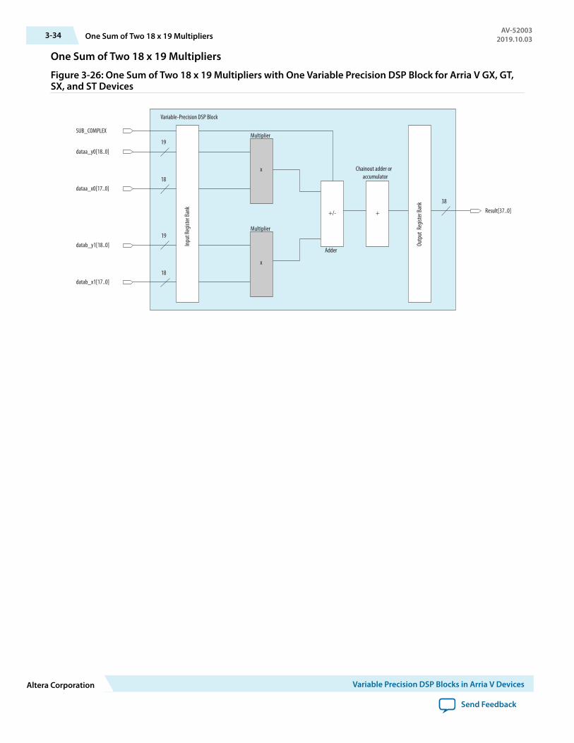
One Sum of Two 18 x 19 Multipliers
Figure 3-26: One Sum of Two 18 x 19 Multipliers with One Variable Precision DSP Block for Arria V GX, GT,SX, and ST Devices
Inpu
t Reg
ister
Bank Result[37..0]
dataa_y0[18..0]
dataa_x0[17..0]
19
18
Variable-Precision DSP Block
datab_y1[18..0]
datab_x1[17..0]
19
18
38
Multiplier
Multiplier
Adder
+/-
Chainout adder oraccumulator
SUB_COMPLEX
Outp
ut R
egist
er Ba
nk
+
x
x
3-34 One Sum of Two 18 x 19 MultipliersAV-52003
2019.10.03
Altera Corporation Variable Precision DSP Blocks in Arria V Devices
Send Feedback

One Sum of Two 27 x 27 Multipliers
Figure 3-27: One Sum of Two 27 x 27 Multipliers with Two Variable Precision DSP Blocks for Arria V GZDevices
Variable Precision DSP Block 2
Variable Precision DSP Block 1
Multiplier
x
Result[54..0]55
Outp
ut Re
giste
r Ban
k
x +
Multiplier Chainout adder
Chainout[53..0]
dataa_0[26..0]
datab_0[26..0]
dataa_1[26..0]
NEGATE
datab_1[26..0]
Inpu
t Reg
ister
Bank
Inpu
t Reg
ister
Bank
27
27
27
27
+/-
AV-520032019.10.03 One Sum of Two 27 x 27 Multipliers 3-35
Variable Precision DSP Blocks in Arria V Devices Altera Corporation
Send Feedback
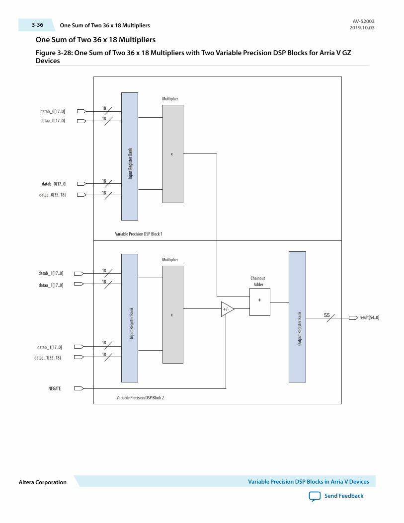
One Sum of Two 36 x 18 Multipliers
Figure 3-28: One Sum of Two 36 x 18 Multipliers with Two Variable Precision DSP Blocks for Arria V GZDevices
Inpu
t Reg
ister
Bank
Inpu
t Reg
ister
Bank
Outp
ut Re
giste
r Ban
k
dataa_0[35..18]
datab_1[17..0]
datab_1[17..0]
dataa_1[35..18]
NEGATE
Variable Precision DSP Block 1
Variable Precision DSP Block 2
result[54..0]
datab_0[17..0]
dataa_0[17..0]
datab_0[17..0]
dataa_1[17..0]
Multiplier
x
Multiplier
x
Chainout Adder
+
18
18
18
18
18
18
55
18
18
+/-
3-36 One Sum of Two 36 x 18 MultipliersAV-52003
2019.10.03
Altera Corporation Variable Precision DSP Blocks in Arria V Devices
Send Feedback

One Sum of Four 18 x 18 Multipliers
Figure 3-29: One Sum of Four 18 x 18 Multipliers with Two Variable Precision DSP Blocks for Arria V GZDevices
result[37..0]
Inpu
t Reg
ister
Bank
18
18
Variable Precision DSP Block 1
18
18
Multiplier
Adder
SUB
18
18
Variable Precision DSP Block 2
18
38
18
SUB
x
x
+/-
Inpu
t Reg
ister
Bank
Outp
ut Re
giste
r Ban
k
Adder
Chainout adderx
x
+/- +
dataa_1[17..0]
datab_2[17..0]
datab_3[17..0]
dataa_3[17..0]
NEGATE
datab_1[17..0]
dataa_0[17..0]
datab_0[17..0]
dataa_2[17..0]
+/-
Multiplier
Multiplier
Multiplier
Sum of Square ModeThe Arria V variable precision DSP block can implement one sum of square mode.
AV-520032019.10.03 One Sum of Four 18 x 18 Multipliers 3-37
Variable Precision DSP Blocks in Arria V Devices Altera Corporation
Send Feedback
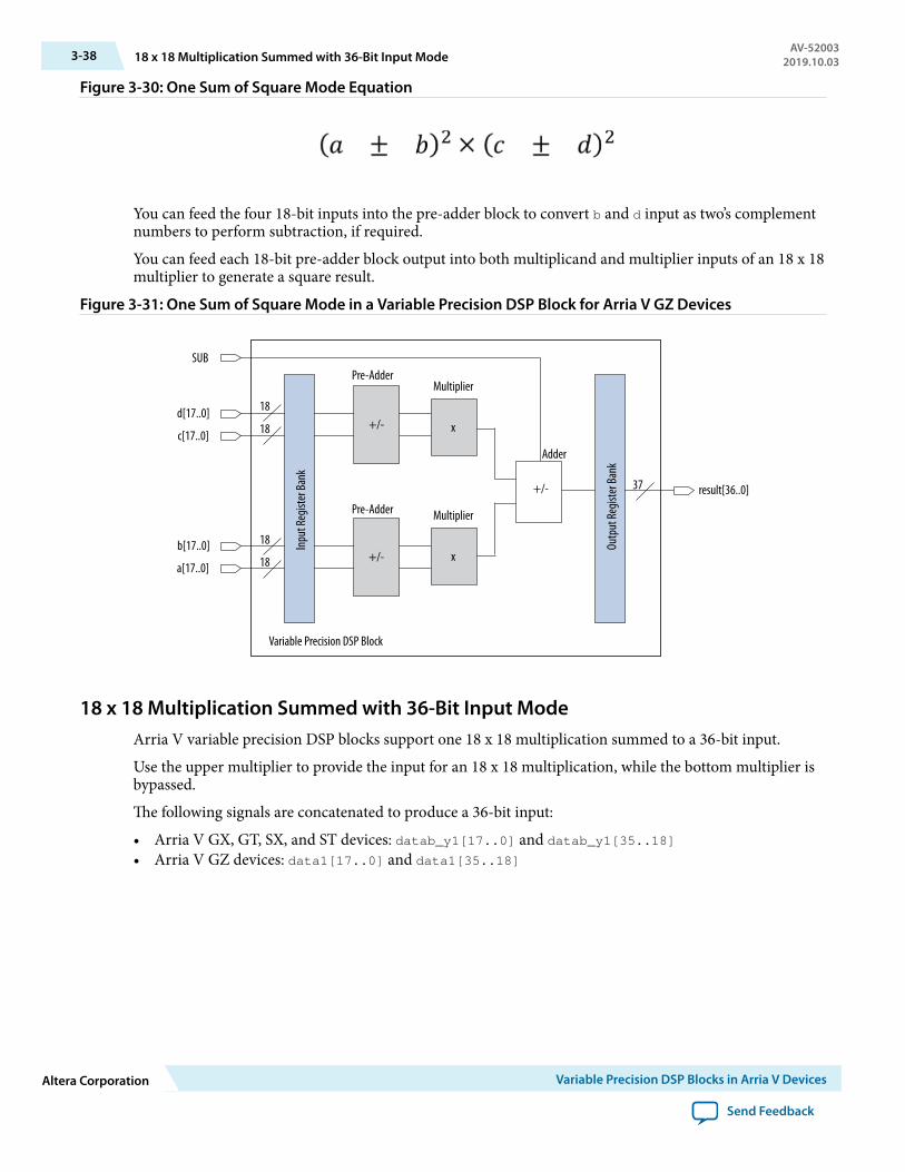
Figure 3-30: One Sum of Square Mode Equation
You can feed the four 18-bit inputs into the pre-adder block to convert b and d input as two’s complementnumbers to perform subtraction, if required.
You can feed each 18-bit pre-adder block output into both multiplicand and multiplier inputs of an 18 x 18multiplier to generate a square result.
Figure 3-31: One Sum of Square Mode in a Variable Precision DSP Block for Arria V GZ Devices
Multiplier
result[36..0]
b[17..0]
a[17..0]
Multiplier
x
Adder
Pre-Adder
d[17..0]
SUB
c[17..0]+/-
Pre-Adder
Variable Precision DSP Block
+/-
+/-
Inpu
t Reg
ister
Bank
Outp
ut Re
giste
r Ban
k
18
37
18
18
18
x
18 x 18 Multiplication Summed with 36-Bit Input ModeArria V variable precision DSP blocks support one 18 x 18 multiplication summed to a 36-bit input.
Use the upper multiplier to provide the input for an 18 x 18 multiplication, while the bottom multiplier isbypassed.
The following signals are concatenated to produce a 36-bit input:
• Arria V GX, GT, SX, and ST devices: datab_y1[17..0] and datab_y1[35..18]• Arria V GZ devices: data1[17..0] and data1[35..18]
3-38 18 x 18 Multiplication Summed with 36-Bit Input ModeAV-52003
2019.10.03
Altera Corporation Variable Precision DSP Blocks in Arria V Devices
Send Feedback
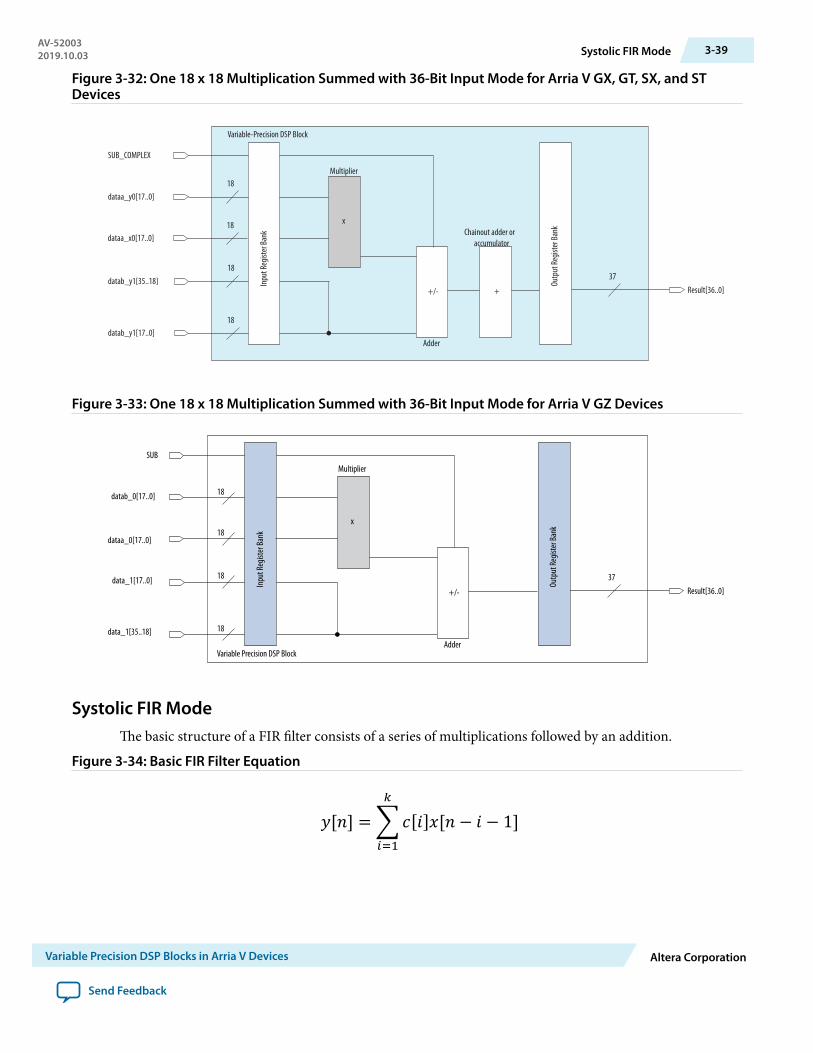
Figure 3-32: One 18 x 18 Multiplication Summed with 36-Bit Input Mode for Arria V GX, GT, SX, and STDevices
Inpu
t Reg
ister
Bank
Result[36..0]
dataa_y0[17..0]
dataa_x0[17..0]
18
18
Variable-Precision DSP Block
datab_y1[35..18]
datab_y1[17..0]
18
18
37
Multiplier
Adder
Chainout adder oraccumulator
SUB_COMPLEX
Outp
ut Re
giste
r Ban
k
x
+/- +
Figure 3-33: One 18 x 18 Multiplication Summed with 36-Bit Input Mode for Arria V GZ Devices
data_1[35..18]
data_1[17..0]
dataa_0[17..0]
datab_0[17..0]
Inpu
t Reg
ister
Bank
Result[36..0]
Variable Precision DSP Block
3718
18
18
18
Multiplier
Adder
SUB
Outp
ut Re
giste
r Ban
k
x
+/-
Systolic FIR ModeThe basic structure of a FIR filter consists of a series of multiplications followed by an addition.
Figure 3-34: Basic FIR Filter Equation
AV-520032019.10.03 Systolic FIR Mode 3-39
Variable Precision DSP Blocks in Arria V Devices Altera Corporation
Send Feedback
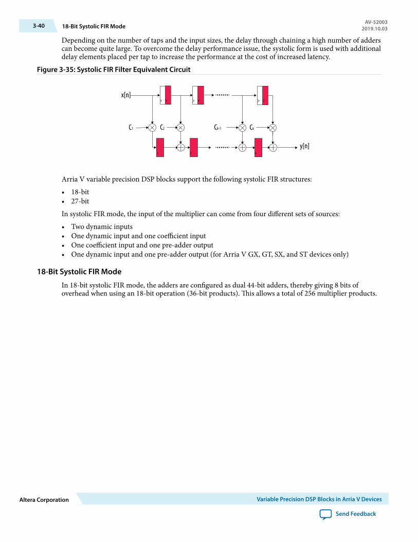
Depending on the number of taps and the input sizes, the delay through chaining a high number of adderscan become quite large. To overcome the delay performance issue, the systolic form is used with additionaldelay elements placed per tap to increase the performance at the cost of increased latency.
Figure 3-35: Systolic FIR Filter Equivalent Circuit
x[n]
y[n]
C1 C2 Ck-1 Ck
Arria V variable precision DSP blocks support the following systolic FIR structures:
• 18-bit• 27-bit
In systolic FIR mode, the input of the multiplier can come from four different sets of sources:
• Two dynamic inputs• One dynamic input and one coefficient input• One coefficient input and one pre-adder output• One dynamic input and one pre-adder output (for Arria V GX, GT, SX, and ST devices only)
18-Bit Systolic FIR Mode
In 18-bit systolic FIR mode, the adders are configured as dual 44-bit adders, thereby giving 8 bits ofoverhead when using an 18-bit operation (36-bit products). This allows a total of 256 multiplier products.
3-40 18-Bit Systolic FIR ModeAV-52003
2019.10.03
Altera Corporation Variable Precision DSP Blocks in Arria V Devices
Send Feedback

Figure 3-36: 18-Bit Systolic FIR Mode for Arria V GX, GT, SX, and ST Devices
Inpu
t Reg
ister
Bank
dataa_y0[17..0]
dataa_z0[17..0]
dataa_x0[17..0]
COEFSELA[2..0]
datab_y1[17..0]
datab_z1[17..0]
datab_x1[17..0]
COEFSELB[2..0]
+/-
Pre-Adder
+/-
Pre-Adder
+/-
InternalCoefficient
InternalCoefficient
Multiplier
Multiplier
Adder
+/-
Systolic Registers (1)
Systolic Register (1)
Chainout adder oraccumulator
+
Outp
ut Re
giste
r Ban
k
chainin[43..0]
chainout[43..0]
Result[43..0]
18-bit Systolic FIR
x
x
Note:1. The systolic registers have the same clock source as the output register bank.
18
18
18
18
18
18
3
3
44
44
44
AV-520032019.10.03 18-Bit Systolic FIR Mode 3-41
Variable Precision DSP Blocks in Arria V Devices Altera Corporation
Send Feedback
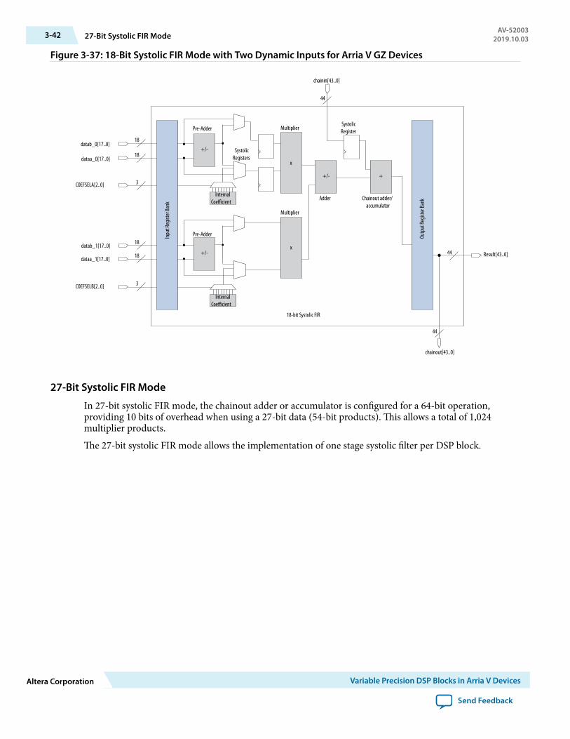
Figure 3-37: 18-Bit Systolic FIR Mode with Two Dynamic Inputs for Arria V GZ Devices
Inpu
t Reg
ister
Bank
Outp
ut Re
giste
r Ban
k
COEFSELA[2..0]
COEFSELB[2..0]
+/-
Pre-Adder
+/-
Pre-Adder
+/-
InternalCoefficient
InternalCoefficient
Multiplier
Multiplier
Adder
+/-
Systolic Registers
Systolic Register
Chainout adder/accumulator
+
chainin[43..0]
chainout[43..0]
Result[43..0]
18-bit Systolic FIR
x
x
datab_0[17..0]
dataa_0[17..0]
datab_1[17..0]
dataa_1[17..0]
18
18
18
18
3
44
3
44
44
27-Bit Systolic FIR Mode
In 27-bit systolic FIR mode, the chainout adder or accumulator is configured for a 64-bit operation,providing 10 bits of overhead when using a 27-bit data (54-bit products). This allows a total of 1,024multiplier products.
The 27-bit systolic FIR mode allows the implementation of one stage systolic filter per DSP block.
3-42 27-Bit Systolic FIR ModeAV-52003
2019.10.03
Altera Corporation Variable Precision DSP Blocks in Arria V Devices
Send Feedback

Figure 3-38: 27-Bit Systolic FIR Mode for Arria V GX, GT, SX, and ST Devices
Inpu
t Reg
ister
Bank
dataa_y0[25..0]
dataa_z0[25..0]
dataa_x0[26..0]
COEFSELA[2..0]
Pre-Adder
+/-
InternalCoefficient
Multiplier
Adder
+/-
Chainout adder oraccumulator
+
chainin[63..0]
chainout[63..0]
27-bit Systolic FIR
27 x
Outp
ut Re
giste
r Ban
k
26
3
27
26
64
64
Figure 3-39: 27-Bit Systolic FIR Mode for Arria V GZ Devices
Inpu
t Reg
ister
Bank
COEFSELA[2..0]
Pre-Adder
+/-
InternalCoefficient
Multiplier
Chainout adder oraccumulator
+
chainin[63..0]
chainout[63..0]
27-bit Systolic FIR
27 x
Outp
ut Re
giste
r Ban
kdatab_0[26..0]
dataa_0[26..0]
datac_0[24..0]
27
3
25
27
64
64
Variable Precision DSP Blocks in Arria V Devices Revision History
Date Version Changes
December2015
2015.12.21 Changed instances of Quartus II to Quartus Prime.
June 2015 2015.06.12 • Updated Systolic FIR Filter Equivalent Circuit figure.
AV-520032019.10.03 Variable Precision DSP Blocks in Arria V Devices Revision History 3-43
Variable Precision DSP Blocks in Arria V Devices Altera Corporation
Send Feedback

Date Version Changes
May 2015 2015.05.08 Added footnote in Features section to clarify certain features are onlyapplicable to certain Arria V device variant.
June 2014 2014.06.30 Updated the supported megafunctions from ALTMULT_ADD andALTMULT _ACCUM to ALTERA_MULT_ADD.
May 2013 2013.05.06 • Added link to the known document issues in the Knowledge Base.• Moved all links to the Related Information section of respective topics
for easy reference.• Updated the variable DSP blocks and multipliers counts for the Arria
V SX and ST device variants.• Updated Figure 3-21, changed 37 to 38.• Updated Figure 3-22 by changing the Complex Multiplication
Equation.• Update Figure 3-26, changed 37 to 38.
November2012
2012.11.29 • Added resources for Arria V devices.• Updated design considerations for Arria V devices in operational
modes.• Added DSP block architecture in 27 x 27 mode for Arria V GX, GT,
SX, and ST devices.• Added DSP block architecture in 18 x 18 and 27 x 27 modes for
Arria V GZ devices.• Updated DSP block architecture information on input register bank,
pre-adder, multipliers, accumulator and chainout adder, and systolicregisters for Arria V GZ devices.
• Added 16 x 16, 18 x 18 (partial), 18 x 18, 36 x 18, and 36-bitindependent multiplier modes for Arria V GZ devices.
• Added 18 x 18, 18 x 25, and 27 x 27 independent complex multipliermodes for Arria V GZ devices.
• Added 16 x 16, 18 x 18, 27 x 27, and 36 x 18 multiplier adder summodes for Arria V GZ devices.
• Added sum of square mode for Arria V GZ devices.• Added 18 x 18 multiplication summed with 36-bit input mode for
Arria V GZ devices.• Added 18-bit and 27-bit systolic FIR modes for Arria V GZ devices.• Reorganized content and updated template.
3-44 Variable Precision DSP Blocks in Arria V Devices Revision HistoryAV-52003
2019.10.03
Altera Corporation Variable Precision DSP Blocks in Arria V Devices
Send Feedback
Date Version Changes
June 2012 2.0 Updated for the Quartus II software v12.0 release:
• Restructured chapter.• Added “Design Considerations”, “Adder”, and “Double Accumulation
Register” sections.• Updated Figure 3–1 and Figure 3–13.• Added Table 3–3.• Updated “Systolic Registers” and “Systolic FIR Mode” sections.• Added Equation 3–2.• Added Figure 3–12.
May 2011 1.0 Initial release.
AV-520032019.10.03 Variable Precision DSP Blocks in Arria V Devices Revision History 3-45
Variable Precision DSP Blocks in Arria V Devices Altera Corporation
Send Feedback
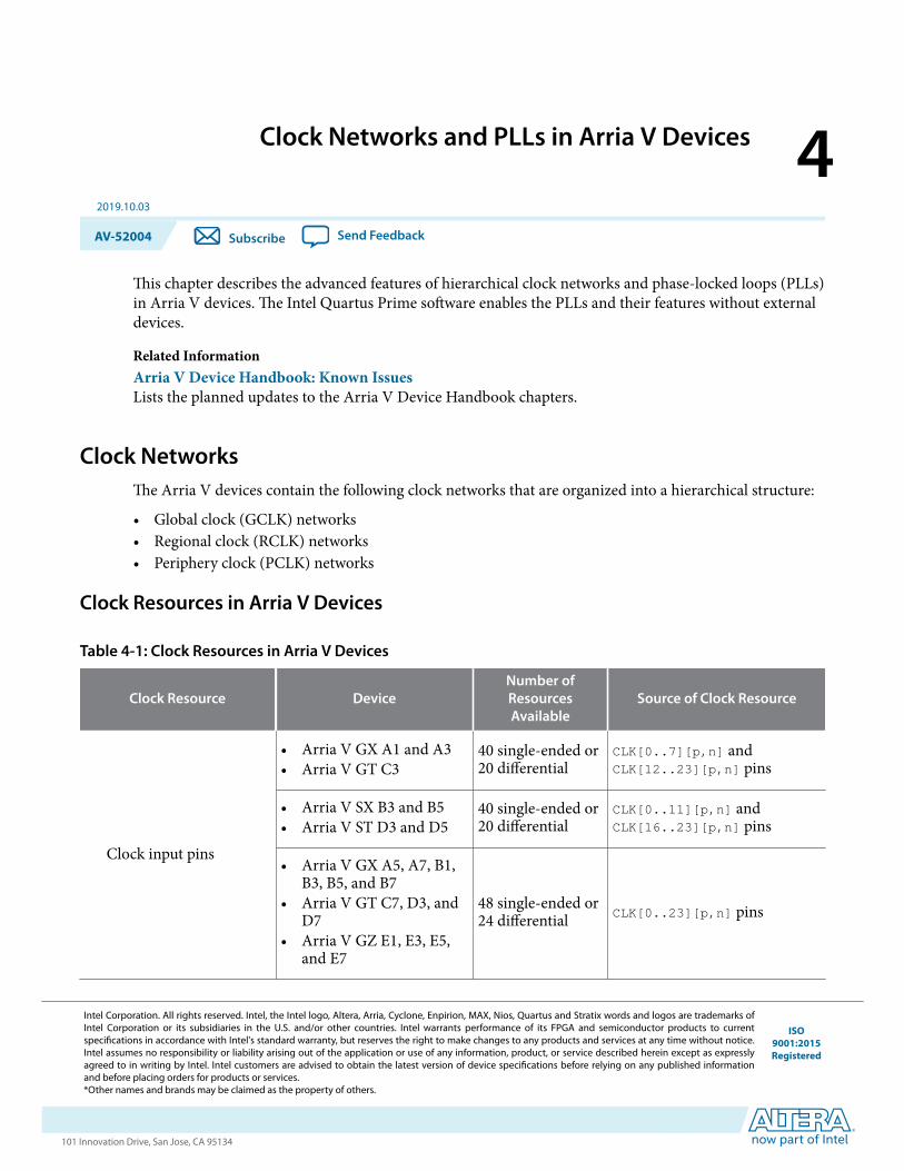
Clock Networks and PLLs in Arria V Devices 42019.10.03
AV-52004 Subscribe Send Feedback
This chapter describes the advanced features of hierarchical clock networks and phase-locked loops (PLLs)in Arria V devices. The Intel Quartus Prime software enables the PLLs and their features without externaldevices.
Related InformationArria V Device Handbook: Known IssuesLists the planned updates to the Arria V Device Handbook chapters.
Clock NetworksThe Arria V devices contain the following clock networks that are organized into a hierarchical structure:
• Global clock (GCLK) networks• Regional clock (RCLK) networks• Periphery clock (PCLK) networks
Clock Resources in Arria V Devices
Table 4-1: Clock Resources in Arria V Devices
Clock Resource DeviceNumber ofResourcesAvailable
Source of Clock Resource
Clock input pins
• Arria V GX A1 and A3• Arria V GT C3
40 single-ended or20 differential
CLK[0..7][p,n] andCLK[12..23][p,n] pins
• Arria V SX B3 and B5• Arria V ST D3 and D5
40 single-ended or20 differential
CLK[0..11][p,n] andCLK[16..23][p,n] pins
• Arria V GX A5, A7, B1,B3, B5, and B7
• Arria V GT C7, D3, andD7
• Arria V GZ E1, E3, E5,and E7
48 single-ended or24 differential CLK[0..23][p,n] pins
Intel Corporation. All rights reserved. Intel, the Intel logo, Altera, Arria, Cyclone, Enpirion, MAX, Nios, Quartus and Stratix words and logos are trademarks ofIntel Corporation or its subsidiaries in the U.S. and/or other countries. Intel warrants performance of its FPGA and semiconductor products to currentspecifications in accordance with Intel's standard warranty, but reserves the right to make changes to any products and services at any time without notice.Intel assumes no responsibility or liability arising out of the application or use of any information, product, or service described herein except as expresslyagreed to in writing by Intel. Intel customers are advised to obtain the latest version of device specifications before relying on any published informationand before placing orders for products or services.*Other names and brands may be claimed as the property of others.
ISO9001:2015Registered
www.altera.com101 Innovation Drive, San Jose, CA 95134
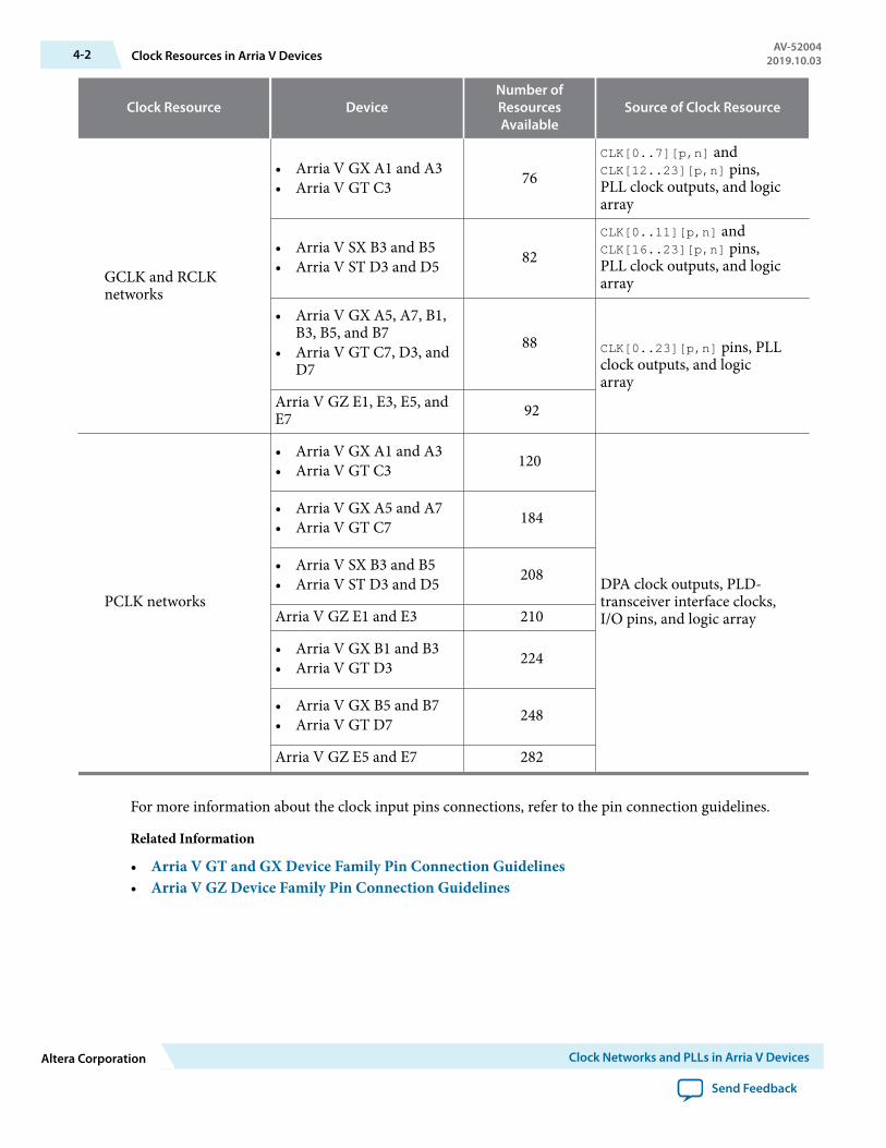
Clock Resource DeviceNumber ofResourcesAvailable
Source of Clock Resource
GCLK and RCLKnetworks
• Arria V GX A1 and A3• Arria V GT C3 76
CLK[0..7][p,n] andCLK[12..23][p,n] pins,PLL clock outputs, and logicarray
• Arria V SX B3 and B5• Arria V ST D3 and D5 82
CLK[0..11][p,n] andCLK[16..23][p,n] pins,PLL clock outputs, and logicarray
• Arria V GX A5, A7, B1,B3, B5, and B7
• Arria V GT C7, D3, andD7
88 CLK[0..23][p,n] pins, PLLclock outputs, and logicarray
Arria V GZ E1, E3, E5, andE7 92
PCLK networks
• Arria V GX A1 and A3• Arria V GT C3 120
DPA clock outputs, PLD-transceiver interface clocks,I/O pins, and logic array
• Arria V GX A5 and A7• Arria V GT C7 184
• Arria V SX B3 and B5• Arria V ST D3 and D5 208
Arria V GZ E1 and E3 210
• Arria V GX B1 and B3• Arria V GT D3 224
• Arria V GX B5 and B7• Arria V GT D7 248
Arria V GZ E5 and E7 282
For more information about the clock input pins connections, refer to the pin connection guidelines.
Related Information
• Arria V GT and GX Device Family Pin Connection Guidelines• Arria V GZ Device Family Pin Connection Guidelines
4-2 Clock Resources in Arria V DevicesAV-52004
2019.10.03
Altera Corporation Clock Networks and PLLs in Arria V Devices
Send Feedback
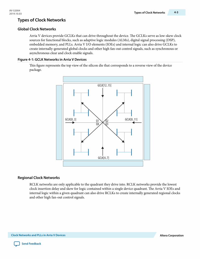
Types of Clock Networks
Global Clock Networks
Arria V devices provide GCLKs that can drive throughout the device. The GCLKs serve as low-skew clocksources for functional blocks, such as adaptive logic modules (ALMs), digital signal processing (DSP),embedded memory, and PLLs. Arria V I/O elements (IOEs) and internal logic can also drive GCLKs tocreate internally-generated global clocks and other high fan-out control signals, such as synchronous orasynchronous clear and clock enable signals.
Figure 4-1: GCLK Networks in Arria V Devices
This figure represents the top view of the silicon die that corresponds to a reverse view of the devicepackage.
GCLK[12..15]
GCLK[8..11]
GCLK[4..7]
GCLK[0..3] Q1Q4
Q2Q3
Regional Clock Networks
RCLK networks are only applicable to the quadrant they drive into. RCLK networks provide the lowestclock insertion delay and skew for logic contained within a single device quadrant. The Arria V IOEs andinternal logic within a given quadrant can also drive RCLKs to create internally generated regional clocksand other high fan-out control signals.
AV-520042019.10.03 Types of Clock Networks 4-3
Clock Networks and PLLs in Arria V Devices Altera Corporation
Send Feedback
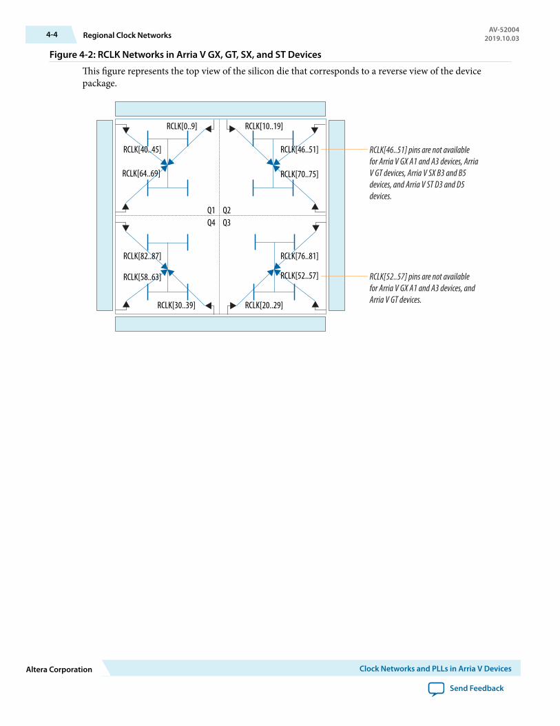
Figure 4-2: RCLK Networks in Arria V GX, GT, SX, and ST Devices
This figure represents the top view of the silicon die that corresponds to a reverse view of the devicepackage.
RCLK[64..69] RCLK[70..75]
RCLK[82..87] RCLK[76..81]
RCLK[58..63] RCLK[52..57]
RCLK[40..45] RCLK[46..51]
RCLK[0..9] RCLK[10..19]
RCLK[30..39] RCLK[20..29]
Q1 Q2Q3Q4
RCLK[46..51] pins are not available for Arria V GX A1 and A3 devices, Arria V GT devices, Arria V SX B3 and B5 devices, and Arria V ST D3 and D5 devices.
RCLK[52..57] pins are not available for Arria V GX A1 and A3 devices, and Arria V GT devices.
4-4 Regional Clock NetworksAV-52004
2019.10.03
Altera Corporation Clock Networks and PLLs in Arria V Devices
Send Feedback
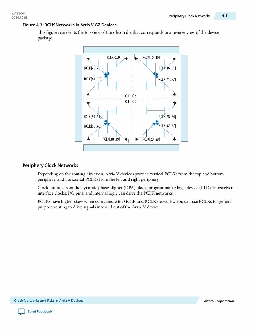
Figure 4-3: RCLK Networks in Arria V GZ Devices
This figure represents the top view of the silicon die that corresponds to a reverse view of the devicepackage.
RCLK[64..70] RCLK[71..77]
RCLK[85..91] RCLK[78..84]
RCLK[58..63] RCLK[52..57]
RCLK[40..45] RCLK[46..51]
RCLK[0..9] RCLK[10..19]
RCLK[30..39] RCLK[20..29]
Q1 Q2Q3Q4
Periphery Clock Networks
Depending on the routing direction, Arria V devices provide vertical PCLKs from the top and bottomperiphery, and horizontal PCLKs from the left and right periphery.
Clock outputs from the dynamic phase aligner (DPA) block, programmable logic device (PLD)-transceiverinterface clocks, I/O pins, and internal logic can drive the PCLK networks.
PCLKs have higher skew when compared with GCLK and RCLK networks. You can use PCLKs for generalpurpose routing to drive signals into and out of the Arria V device.
AV-520042019.10.03 Periphery Clock Networks 4-5
Clock Networks and PLLs in Arria V Devices Altera Corporation
Send Feedback

Figure 4-4: PCLK Networks in Arria V Devices
This figure represents the top view of the silicon die that corresponds to a reverse view of the devicepackage.
Q1 Q2
Q4 Q3
Horizontal PCLK
Horizontal PCLK
Horizontal PCLK
Horizontal PCLK
Vertical PCLK
Vertical PCLK
Verti
cal P
CLK
Verti
cal P
CLK
Verti
cal P
CLK
Vertical PCLK
Horizontal PCLK
Horizontal PCLK
HorizontalPCLK
Horizontal PCLK
Verti
cal P
CLK
Vertical PCLK
Clock Sources Per QuadrantThe Arria V devices provide 30 section clock (SCLK) networks in each spine clock per quadrant. TheSCLK networks can drive six row clocks in each logic array block (LAB) row, nine column I/O clocks, andtwo core reference clocks. The SCLKs are the clock resources to the core functional blocks, PLLs, and I/Ointerfaces of the device.
A spine clock is another layer of routing between the GCLK, RCLK, and PCLK networks before each clockis connected to the clock routing for each LAB row. The settings for spine clocks are transparent. The IntelQuartus Prime software automatically routes the spine clock based on the GCLK, RCLK, and PCLKnetworks.
The following figure shows SCLKs driven by the GCLK, RCLK, PCLK, or the PLL feedback clock networksin each spine clock per quadrant. The GCLK, RCLK, PCLK, and PLL feedback clocks share the samerouting to the SCLKs. To ensure successful design fitting in the Intel Quartus Prime software, the totalnumber of clock resources must not exceed the SCLK limits in each region.
4-6 Clock Sources Per QuadrantAV-52004
2019.10.03
Altera Corporation Clock Networks and PLLs in Arria V Devices
Send Feedback

Figure 4-5: Hierarchical Clock Networks in Each Spine Clock Per Quadrant
SCLK
Column I/O clock: clock that drives the I/O column core registers and I/O interfaces.
Core reference clock: clock that feeds into the PLL as the PLL reference clock.
Row clock: clock source to the LAB, memory blocks, and row I/O interfaces in the core row.
GCLK
RCLK
PLL Feedback Clock PCLK
9
230
16
5
72
23
6
Clock output from the PLL thatdrives into the SCLKs.
There are up to 72 PCLKs that can drive the SCLKs in each spine clock per quadrant in the largest device.There are up to 23 RCLKs that can drive the SCLKs in each spine clock per quadrant in the largest device.
Types of Clock RegionsThis section describes the types of clock regions in Arria V devices.
Entire Device Clock Region
To form the entire device clock region, a source drives a signal in a GCLK network that can be routedthrough the entire device. The source is not necessarily a clock signal. This clock region has the maximuminsertion delay when compared with other clock regions, but allows the signal to reach every destinationin the device. It is a good option for routing global reset and clear signals or routing clocks throughout thedevice.
Regional Clock Region
To form a regional clock region, a source drives a signal in a RCLK network that you can route throughoutone quadrant of the device. This clock region provides the lowest skew in a quadrant. It is a good option ifall the destinations are in a single quadrant.
Dual-Regional Clock Region
To form a dual-regional clock region, a single source (a clock pin or PLL output) generates a dual-regionalclock by driving two RCLK networks (one from each quadrant). This technique allows destinations acrosstwo adjacent device quadrants to use the same low-skew clock. The routing of this signal on an entire sidehas approximately the same delay as a RCLK region. Internal logic can also drive a dual-regional clocknetwork.
AV-520042019.10.03 Types of Clock Regions 4-7
Clock Networks and PLLs in Arria V Devices Altera Corporation
Send Feedback
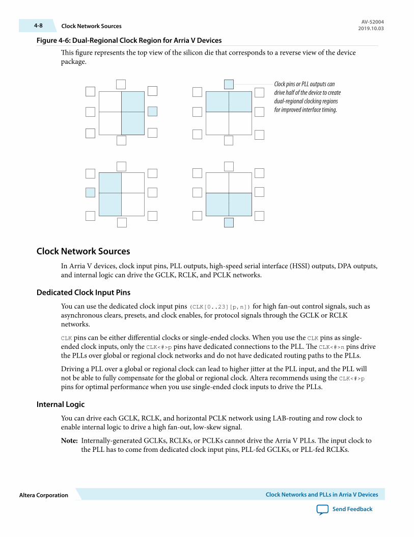
Figure 4-6: Dual-Regional Clock Region for Arria V Devices
This figure represents the top view of the silicon die that corresponds to a reverse view of the devicepackage.
Clock pins or PLL outputs can drive half of the device to createdual-regional clocking regionsfor improved interface timing.
Clock Network SourcesIn Arria V devices, clock input pins, PLL outputs, high-speed serial interface (HSSI) outputs, DPA outputs,and internal logic can drive the GCLK, RCLK, and PCLK networks.
Dedicated Clock Input Pins
You can use the dedicated clock input pins (CLK[0..23][p,n]) for high fan-out control signals, such asasynchronous clears, presets, and clock enables, for protocol signals through the GCLK or RCLKnetworks.
CLK pins can be either differential clocks or single-ended clocks. When you use the CLK pins as single-ended clock inputs, only the CLK<#>p pins have dedicated connections to the PLL. The CLK<#>n pins drivethe PLLs over global or regional clock networks and do not have dedicated routing paths to the PLLs.
Driving a PLL over a global or regional clock can lead to higher jitter at the PLL input, and the PLL willnot be able to fully compensate for the global or regional clock. Altera recommends using the CLK<#>ppins for optimal performance when you use single-ended clock inputs to drive the PLLs.
Internal Logic
You can drive each GCLK, RCLK, and horizontal PCLK network using LAB-routing and row clock toenable internal logic to drive a high fan-out, low-skew signal.
Note: Internally-generated GCLKs, RCLKs, or PCLKs cannot drive the Arria V PLLs. The input clock tothe PLL has to come from dedicated clock input pins, PLL-fed GCLKs, or PLL-fed RCLKs.
4-8 Clock Network SourcesAV-52004
2019.10.03
Altera Corporation Clock Networks and PLLs in Arria V Devices
Send Feedback

DPA Outputs
Every DPA generates one PCLK to the core.
Related InformationHigh-Speed I/O Design Guidelines for Arria V Devices on page 6-7Provides more information about DPA and HSSI outputs.
HSSI Outputs
Every three HSSI outputs generate a group of six PCLKs to the core.
Related InformationHigh-Speed I/O Design Guidelines for Arria V Devices on page 6-7Provides more information about DPA and HSSI outputs.
PLL Clock Outputs
The Arria V PLL clock outputs can drive both GCLK and RCLK networks.
Clock Input Pin Connections to GCLK and RCLK Networks
Table 4-2: Dedicated Clock Input Pin Connectivity to the GCLK Networks for Arria V Devices
Clock Resources CLK (p/n Pins)
GCLK[0,1,2,3] CLK[0,1,2,3,20,21,22,23]
GCLK[4,5,6,7] CLK[4,5,6,7]
GCLK[8,9,10,11] CLK[8,9,10,11] and (5) CLK[12,13,14,15](6)
GCLK[12,13,14,15] CLK[16,17,18,19]
Table 4-3: Dedicated Clock Input Pin Connectivity to the RCLK Networks for Arria V GX, GT, SX, and STDevices
A given clock input pin can drive two adjacent RCLK networks to create a dual-regional clock network.Clock Resources CLK (p/n Pins)
RCLK[58,59,60,61,62,63,64,68,82,86] CLK[0]
RCLK[58,59,60,61,62,63,65,69,83,87] CLK[1]
RCLK[58,59,60,61,62,63,66,84] CLK[2]
RCLK[58,59,60,61,62,63,67,85] CLK[3]
RCLK[20,24,28,30,34,38] CLK[4]
RCLK[21,25,29,31,35,39] CLK[5]
RCLK[22,26,32,36] CLK[6]
(5) CLK[8,9,10,11] are not available for Arria V GX A1 and A3 devices, and Arria V GT devices.(6) CLK[12,13,14,15] are not available for Arria V Arria V SX B3 and B5 devices, and Arria V ST D3 and
D5 devices.
AV-520042019.10.03 DPA Outputs 4-9
Clock Networks and PLLs in Arria V Devices Altera Corporation
Send Feedback

Clock Resources CLK (p/n Pins)
RCLK[23,27,33,37] CLK[7]
RCLK[52,53,54,55,56,57,70,74,76,80] CLK[8] (5)
RCLK[52,53,54,55,56,57,71,75,77,81] CLK[9] (5)
RCLK[52,53,54,55,56,57,72,78] CLK[10] (5)
RCLK[52,53,54,55,56,57,73,79] CLK[11] (5)
RCLK[46,47,48,49,50,51,70,74,76,80] (7) CLK[12] (6)
RCLK[46,47,48,49,50,51,71,75,77,81] (7) CLK[13] (6)
RCLK[46,47,48,49,50,51,72,78] (7) CLK[14] (6)
RCLK[46,47,48,49,50,51,73,79] (7) CLK[15] (6)
RCLK[0,4,8,10,14,18] CLK[16]
RCLK[1,5,9,11,15,19] CLK[17]
RCLK[2,6,12,16] CLK[18]
RCLK[3,7,13,17] CLK[19]
RCLK[40,41,42,43,44,45,64,68,82,86] CLK[20]
RCLK[40,41,42,43,44,45,65,69,83,87] CLK[21]
RCLK[40,41,42,43,44,45,66,84] CLK[22]
RCLK[40,41,42,43,44,45,67,85] CLK[23]
Table 4-4: Dedicated Clock Input Pin Connectivity to the RCLK Networks for Arria V GZ Devices
A given clock input pin can drive two adjacent RCLK networks to create a dual-regional clock network.Clock Resources CLK (p/n Pins)
RCLK[58,59,60,61,62,63,64,68,85,89] CLK[0]
RCLK[58,59,60,61,62,63,65,69,86,90] CLK[1]
RCLK[58,59,60,61,62,63,66,70,87,91] CLK[2]
RCLK[58,59,60,61,62,63,67,88] CLK[3]
RCLK[20,24,28,30,34,38] CLK[4]
RCLK[21,25,29,31,35,39] CLK[5]
RCLK[22,26,32,36] CLK[6]
RCLK[23,27,33,37] CLK[7]
RCLK[52,53,54,55,56,57,71,75,78,82] CLK[8]
RCLK[52,53,54,55,56,57,72,76,79,83] CLK[9]
RCLK[52,53,54,55,56,57,73,77,80,84] CLK[10]
(7) RCLK[46..51] are not available for Arria V GX A1 and A3 devices, and Arria V GT devices.
4-10 Clock Input Pin Connections to GCLK and RCLK NetworksAV-52004
2019.10.03
Altera Corporation Clock Networks and PLLs in Arria V Devices
Send Feedback

Clock Resources CLK (p/n Pins)
RCLK[52,53,54,55,56,57,74,81] CLK[11]
RCLK[46,47,48,49,50,51,71,75,78,82] CLK[12]
RCLK[46,47,48,49,50,51,72,76,79,83] CLK[13]
RCLK[46,47,48,49,50,51,73,77,80,84] CLK[14]
RCLK[46,47,48,49,50,51,74,81] CLK[15]
RCLK[0,4,8,10,14,18] CLK[16]
RCLK[1,5,9,11,15,19] CLK[17]
RCLK[2,6,12,16] CLK[18]
RCLK[3,7,13,17] CLK[19]
RCLK[40,41,42,43,44,45,64,68,85,89] CLK[20]
RCLK[40,41,42,43,44,45,65,69,86,90] CLK[21]
RCLK[40,41,42,43,44,45,66,70,87,91] CLK[22]
RCLK[40,41,42,43,44,45,67,88] CLK[23]
Clock Output ConnectionsFor Arria V PLL connectivity to GCLK and RCLK networks, refer to the PLL connectivity to GCLK andRCLK networks spreadsheet.
Related InformationPLL Connectivity to GCLK and RCLK Networks for Arria V Devices
Clock Control BlockEvery GCLK, RCLK, and PCLK network has its own clock control block. The control block provides thefollowing features:
• Clock source selection (dynamic selection available only for GCLKs)• Global clock multiplexing• Clock power down (static or dynamic clock enable or disable available only for GCLKs and RCLKs)
Pin Mapping in Arria V Devices
Table 4-5: Mapping Between the Input Clock Pins, PLL Counter Outputs, and Clock Control Block Inputs
Clock Fed by
inclk[0] and inclk[1] Any of the four dedicated clock pins on the same side of the Arria Vdevice.
inclk[2]PLL counters C0 and C2 from the two center PLLs on the same side of theArria V devices.
inclk[3]PLL counters C1 and C3 from the two center PLLs on the same side of theArria V devices.
AV-520042019.10.03 Clock Output Connections 4-11
Clock Networks and PLLs in Arria V Devices Altera Corporation
Send Feedback

Note: You cannot use corner PLLs for dynamic clock control selection.
GCLK Control Block
You can select the clock source for the GCLK select block either statically or dynamically using internallogic to drive the multiplexer-select inputs.
When selecting the clock source dynamically, you can select either PLL outputs (such as C0 or C1), or acombination of clock pins or PLL outputs.
Figure 4-7: GCLK Control Block for Arria V Devices
CLKpPins
PLL CounterOutputs
CLKSELECT[1..0]
2
2
2
GCLK
Enable/ Disable
This multiplexer supports user-controllable dynamic switching
InternalLogic
InternalLogic
Static ClockSelect
CLKnPin
When the device is in user mode, you can dynamically control the clock select signals through internal logic. When the device is in user mode, you can only
set the clock select signals through a configuration file (SRAM object file [.sof] or programmer object file [.pof]) because the signals cannot be controlled dynamically.
The CLKn pin is not a dedicated clock input when used as a single-ended PLL clock input. The CLKn pin can drive the PLL using the GCLK.
RCLK Control Block
You can only control the clock source selection for the RCLK select block statically using configuration bitsettings in the configuration file (.sof or .pof) generated by the Intel Quartus Prime software.
Figure 4-8: RCLK Control Block for Arria V Devices
CLKpPin
PLL CounterOutputs
Internal Logic
CLKnPin
Enable/Disable
RCLK
InternalLogic
Static Clock Select
2
When the device is in user mode, you can only set the clock select signals through a configuration file (.sof or .pof); they cannot be controlled dynamically.
The CLKn pin is not a dedicated clock input when used as a single-ended PLL clock input. The CLKn pin can drive the PLL using the RCLK.
4-12 GCLK Control BlockAV-52004
2019.10.03
Altera Corporation Clock Networks and PLLs in Arria V Devices
Send Feedback
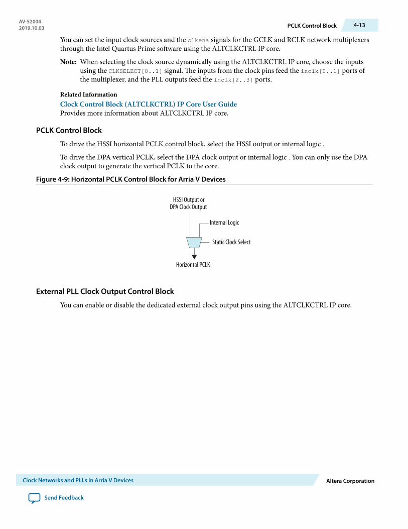
You can set the input clock sources and the clkena signals for the GCLK and RCLK network multiplexersthrough the Intel Quartus Prime software using the ALTCLKCTRL IP core.
Note: When selecting the clock source dynamically using the ALTCLKCTRL IP core, choose the inputsusing the CLKSELECT[0..1] signal. The inputs from the clock pins feed the inclk[0..1] ports ofthe multiplexer, and the PLL outputs feed the inclk[2..3] ports.
Related InformationClock Control Block (ALTCLKCTRL) IP Core User GuideProvides more information about ALTCLKCTRL IP core.
PCLK Control Block
To drive the HSSI horizontal PCLK control block, select the HSSI output or internal logic .
To drive the DPA vertical PCLK, select the DPA clock output or internal logic . You can only use the DPAclock output to generate the vertical PCLK to the core.
Figure 4-9: Horizontal PCLK Control Block for Arria V Devices
HSSI Output orDPA Clock Output
Internal Logic
Static Clock Select
Horizontal PCLK
External PLL Clock Output Control Block
You can enable or disable the dedicated external clock output pins using the ALTCLKCTRL IP core.
AV-520042019.10.03 PCLK Control Block 4-13
Clock Networks and PLLs in Arria V Devices Altera Corporation
Send Feedback
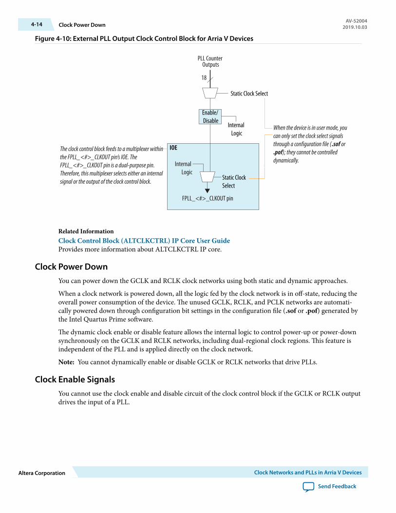
Figure 4-10: External PLL Output Clock Control Block for Arria V Devices
PLL CounterOutputs
FPLL_<#>_CLKOUT pin
IOE
Internal Logic
18
Enable/ Disable
Static Clock Select
Internal Logic
Static Clock Select
When the device is in user mode, you can only set the clock select signals through a configuration file (.sof or .pof); they cannot be controlled dynamically.
The clock control block feeds to a multiplexer within the FPLL_<#>_CLKOUT pin’s IOE. The FPLL_<#>_CLKOUT pin is a dual-purpose pin. Therefore, this multiplexer selects either an internal signal or the output of the clock control block.
Related InformationClock Control Block (ALTCLKCTRL) IP Core User GuideProvides more information about ALTCLKCTRL IP core.
Clock Power DownYou can power down the GCLK and RCLK clock networks using both static and dynamic approaches.
When a clock network is powered down, all the logic fed by the clock network is in off-state, reducing theoverall power consumption of the device. The unused GCLK, RCLK, and PCLK networks are automati‐cally powered down through configuration bit settings in the configuration file (.sof or .pof) generated bythe Intel Quartus Prime software.
The dynamic clock enable or disable feature allows the internal logic to control power-up or power-downsynchronously on the GCLK and RCLK networks, including dual-regional clock regions. This feature isindependent of the PLL and is applied directly on the clock network.
Note: You cannot dynamically enable or disable GCLK or RCLK networks that drive PLLs.
Clock Enable SignalsYou cannot use the clock enable and disable circuit of the clock control block if the GCLK or RCLK outputdrives the input of a PLL.
4-14 Clock Power DownAV-52004
2019.10.03
Altera Corporation Clock Networks and PLLs in Arria V Devices
Send Feedback
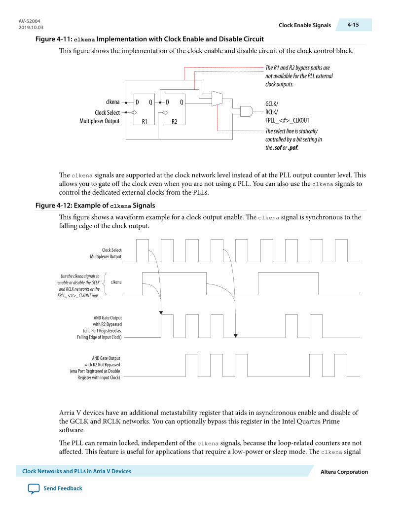
Figure 4-11: clkena Implementation with Clock Enable and Disable Circuit
This figure shows the implementation of the clock enable and disable circuit of the clock control block.
clkena
Clock SelectMultiplexer Output
GCLK/RCLK/FPLL_<#>_CLKOUT
D DQ Q
R1 R2
The R1 and R2 bypass paths are not available for the PLL external clock outputs.
The select line is statically controlled by a bit setting in the .sof or .pof.
The clkena signals are supported at the clock network level instead of at the PLL output counter level. Thisallows you to gate off the clock even when you are not using a PLL. You can also use the clkena signals tocontrol the dedicated external clocks from the PLLs.
Figure 4-12: Example of clkena Signals
This figure shows a waveform example for a clock output enable. The clkena signal is synchronous to thefalling edge of the clock output.
clkena
AND Gate Output with R2 Bypassed
(ena Port Registered as Falling Edge of Input Clock)
Clock SelectMultiplexer Output
AND Gate Outputwith R2 Not Bypassed
(ena Port Registered as DoubleRegister with Input Clock)
Use the clkena signals to enable or disable the GCLK and RCLK networks or the
FPLL_<#>_CLKOUT pins.
Arria V devices have an additional metastability register that aids in asynchronous enable and disable ofthe GCLK and RCLK networks. You can optionally bypass this register in the Intel Quartus Primesoftware.
The PLL can remain locked, independent of the clkena signals, because the loop-related counters are notaffected. This feature is useful for applications that require a low-power or sleep mode. The clkena signal
AV-520042019.10.03 Clock Enable Signals 4-15
Clock Networks and PLLs in Arria V Devices Altera Corporation
Send Feedback

can also disable clock outputs if the system is not tolerant of frequency overshoot during resynchroniza‐tion.
Arria V PLLsPLLs provide robust clock management and synthesis for device clock management, external system clockmanagement, and high-speed I/O interfaces.
The Arria V device family contains fractional PLLs that can function as fractional PLLs or integer PLLs.The output counters in Arria V devices are dedicated to each fractional PLL that support integer orfractional frequency synthesis.
Two adjacent PLLs share 18 C output counters. Any number of C counters can be assigned to each PLL, aslong as the total number used by the two PLLs is 18 or less.
The Arria V devices offer up to 16 fractional PLLs in the larger densities. All Arria V fractional PLLs havethe same core analog structure and features support.
Table 4-6: PLL Features in Arria V Devices
Feature Support
Integer PLL YesFractional PLL YesC output counters 18M, N, C counter sizes 1 to 512Dedicated external clock outputs 4 single-ended or 2 single-ended and 1 differentialDedicated clock input pins 4 single-ended or 4 differentialExternal feedback input pin Single-ended or differentialSpread-spectrum input clock tracking Yes (8)
Source synchronous compensation YesDirect compensation YesNormal compensation YesZero-delay buffer compensation YesExternal feedback compensation YesLVDS compensation YesVoltage-controlled oscillator (VCO) output drivesthe DPA clock Yes
Phase shift resolution 78.125 ps (9)
(8) Provided input clock jitter is within input jitter tolerance specifications. The modulation frequency of theinput clock is below the PLL bandwidth which is specified in the Fitter report.
(9) The smallest phase shift is determined by the VCO period divided by eight. For degree increments, the ArriaV device can shift all output frequencies in increments of at least 45°. Smaller degree increments are possibledepending on the frequency and divide parameters.
4-16 Arria V PLLsAV-52004
2019.10.03
Altera Corporation Clock Networks and PLLs in Arria V Devices
Send Feedback

Feature Support
Programmable duty cycle YesPower down mode Yes
PLL Physical Counters in Arria V DevicesThe physical counters for the fractional PLLs are arranged in the following sequences:
• Up-to-down• Down-to-up
Figure 4-13: PLL Physical Counters Orientation for Arria V DevicesThis figure represents the top view of the silicon die that corresponds to a reverse view of the devicepackage.
PLL0
PLL1
Physical Counter C0
Physical Counter C1
Physical Counter C8
Physical Counter C9
Physical Counter C16
Physical Counter C17
Physical Counter C0 to C17 (Up-to-Down Dequence)
PLL1
PLL0
Physical Counter C17
Physical Counter C16
Physical Counter C9
Physical Counter C8
Physical Counter C1
Physical Counter C0
Physical Counter C17 to C0 (Down-to-Up Sequence)
PLL Locations in Arria V DevicesArria V devices provide PLLs for the transceiver channels. These PLLs are located in a strip, where thestrip refers to an area in the FPGA.
The total number of PLLs in the Arria V devices includes the PLLs in the PLL strip. However, thetransceivers can only use the PLLs located in the strip.
The following figures show the physical locations of the fractional PLLs. Every index represents onefractional PLL in the device. The physical locations of the fractional PLLs correspond to the coordinates inthe Quartus II Chip Planner.
AV-520042019.10.03 PLL Physical Counters in Arria V Devices 4-17
Clock Networks and PLLs in Arria V Devices Altera Corporation
Send Feedback

Figure 4-14: PLL Locations for Arria V GX A1 and A3 Devices, and Arria V GT C3 DeviceThis figure represents the top view of the silicon die that corresponds to a reverse view of the devicepackage.
Pins
Logic
al Clo
cks
4
CLK[
12..1
5][p
,n]
PinsCLK[4..7][p,n]
Logical Clocks4
Pins
4 Logical Clocks
FRACTIONALPLL_XO_Y60FRACTIONALPLL_XO_Y51
4
4
4
Pins
Logical Clocks
Pins
4 Logical Clocks
CLK[20..23][p,n]
CLK[0..3][p,n]
CLK[16..19][p,n]
FRACTIONALPLL_XO_Y18FRACTIONALPLL_XO_Y9
FRACTIONALPLL_X43_Y65FRACTIONALPLL_X43_Y56
FRAC
TIONA
LPLL
_X97
_Y40
FRAC
TIONA
LPLL
_X97
_Y31
FRACTIONALPLL_X43_Y11FRACTIONALPLL_X43_Y2
PLL Strip
Figure 4-15: PLL Locations for Arria V GX A5 and A7 Devices, and Arria V GT C7 DeviceThis figure represents the top view of the silicon die that corresponds to a reverse view of the devicepackage.
FRACTIONALPLL_XO_Y65FRACTIONALPLL_XO_Y56
FRACTIONALPLL_XO_Y23FRACTIONALPLL_XO_Y14
FRACTIONALPLL_X132_Y65FRACTIONALPLL_X132_Y56
FRACTIONALPLL_X132_Y23FRACTIONALPLL_X132_Y14
Logical Clocks4
Pins
4 Logical Clocks
Pins
CLK[16..19][p,n]
CLK[4..7][p,n]
4
4
Pins
Logical Clocks
Pins
4 Logical Clocks
CLK[20..23][p,n]
CLK[0..3][p,n]
4 Logical Clocks
Pins
Pins
Logical Clocks4
CLK[12..15][p,n]
CLK[8..11][p,n]
4
4
4
FRACTIONALPLL_X58_Y76FRACTIONALPLL_X58_Y67
FRACTIONALPLL_X58_Y11FRACTIONALPLL_X58_Y2
PLL Strip PLL Strip
4-18 PLL Locations in Arria V DevicesAV-52004
2019.10.03
Altera Corporation Clock Networks and PLLs in Arria V Devices
Send Feedback
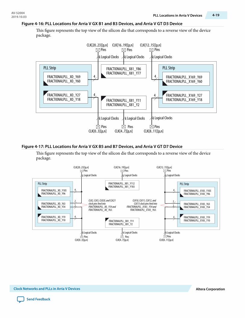
Figure 4-16: PLL Locations for Arria V GX B1 and B3 Devices, and Arria V GT D3 DeviceThis figure represents the top view of the silicon die that corresponds to a reverse view of the devicepackage.
FRACTIONALPLL_XO_Y69FRACTIONALPLL_XO_Y60
FRACTIONALPLL_XO_Y27FRACTIONALPLL_XO_Y18
FRACTIONALPLL_X169_Y69FRACTIONALPLL_X169_Y60
FRACTIONALPLL_X169_Y27FRACTIONALPLL_X169_Y18
Pins
4 Logical Clocks
Pins
CLK[16..19][p,n]
CLK[4..7][p,n]
4
4
4 Logical Clocks
Pins
PinsCLK[12..15][p,n]
CLK[8..11][p,n]
4
Pins
Logical Clocks
PinsCLK[20..23][p,n]
CLK[0..3][p,n]
4 Logical Clocks4 Logical Clocks4 Logical Clocks
4
4
FRACTIONALPLL_X81_Y86FRACTIONALPLL_X81_Y77
FRACTIONALPLL_X81_Y11FRACTIONALPLL_X81_Y2
PLL Strip PLL Strip
Figure 4-17: PLL Locations for Arria V GX B5 and B7 Devices, and Arria V GT D7 DeviceThis figure represents the top view of the silicon die that corresponds to a reverse view of the devicepackage.
PinsCLK[4..7][p,n]
Logical Clocks4
Pins
4 Logical Clocks
4
4
2 2
4PinsLogical Clocks
Pins
4 Logical Clocks
CLK[20..23][p,n]
CLK[0..3][p,n]
CLK[16..19][p,n]
4
4
4 Logical ClocksPins
Pins
Logical Clocks4
CLK[12..15][p,n]
CLK[8..11][p,n]
2
FRACTIONALPLL_XO_Y105FRACTIONALPLL_XO_Y96
FRACTIONALPLL_XO_Y63FRACTIONALPLL_XO_Y54
FRACTIONALPLL_XO_Y19FRACTIONALPLL_XO_Y10
FRACTIONALPLL_X183_Y105FRACTIONALPLL_X183_Y96
FRACTIONALPLL_X183_Y63FRACTIONALPLL_X183_Y54
FRACTIONALPLL_X183_Y19FRACTIONALPLL_X183_Y10
2
FRACTIONALPLL_X81_Y112FRACTIONALPLL_X81_Y103
FRACTIONALPLL_X81_Y11FRACTIONALPLL_X81_Y2
CLK2, CLK3, CLK20, and CLK21 clock pins feed into FRACTIONALPLL_X0_Y54 and FRACTIONALPLL_X0_Y63.
CLK10, CLK11, CLK12, and CLK13 clock pins feed into
FRACTIONALPLL_X183_Y54 and FRACTIONALPLL_X183_Y63.
PLL Strip PLL Strip
AV-520042019.10.03 PLL Locations in Arria V Devices 4-19
Clock Networks and PLLs in Arria V Devices Altera Corporation
Send Feedback
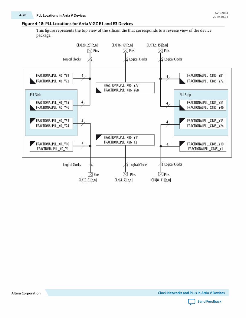
Figure 4-18: PLL Locations for Arria V GZ E1 and E3 DevicesThis figure represents the top view of the silicon die that corresponds to a reverse view of the devicepackage.
PinsCLK[4..7][p,n]
FRACTIONALPLL_X86_Y77FRACTIONALPLL_X86_Y68
FRACTIONALPLL_X86_Y11FRACTIONALPLL_X86_Y2
Logical Clocks4
Pins
4 Logical Clocks
FRACTIONALPLL_X0_Y81FRACTIONALPLL_X0_Y72
FRACTIONALPLL_X0_Y55FRACTIONALPLL_X0_Y46
FRACTIONALPLL_X0_Y33FRACTIONALPLL_X0_Y24
FRACTIONALPLL_X0_Y10FRACTIONALPLL_X0_Y1
4
4
4
4
4
Pins
Logical Clocks
Pins
4Logical Clocks
CLK[20..23][p,n]
CLK[0..3][p,n]
CLK[16..19][p,n]
FRACTIONALPLL_X185_Y81FRACTIONALPLL_X185_Y72
FRACTIONALPLL_X185_Y55FRACTIONALPLL_X185_Y46
FRACTIONALPLL_X185_Y33FRACTIONALPLL_X185_Y24
FRACTIONALPLL_X185_Y10FRACTIONALPLL_X185_Y1
4
4
4
4
4 Logical Clocks
Pins
Pins
Logical Clocks4
CLK[12..15][p,n]
CLK[8..11][p,n]
PLL Strip PLL Strip
4-20 PLL Locations in Arria V DevicesAV-52004
2019.10.03
Altera Corporation Clock Networks and PLLs in Arria V Devices
Send Feedback

Figure 4-19: PLL Locations for Arria V GZ E5 and E7 DevicesThis figure represents the top view of the silicon die that corresponds to a reverse view of the devicepackage.
PinsCLK[4..7][p,n]
FRACTIONALPLL_X92_Y96FRACTIONALPLL_X92_Y87
FRACTIONALPLL_X92_Y11FRACTIONALPLL_X92_Y2
Logical Clocks4
Pins
4 Logical Clocks
FRACTIONALPLL_X0_Y100FRACTIONALPLL_X0_Y91
FRACTIONALPLL_X0_Y77FRACTIONALPLL_X0_Y68
FRACTIONALPLL_X0_Y55FRACTIONALPLL_X0_Y46
FRACTIONALPLL_X0_Y31FRACTIONALPLL_X0_Y22
FRACTIONALPLL_X0_Y10FRACTIONALPLL_X0_Y1
4
4
4
4
2
2
4
Pins
Logical Clocks
Pins
4Logical Clocks
CLK[20..23][p,n]
CLK[0..3][p,n]
CLK[16..19][p,n]
FRACTIONALPLL_X202_Y100FRACTIONALPLL_X202_Y91
FRACTIONALPLL_X202_Y77FRACTIONALPLL_X202_Y68
FRACTIONALPLL_X202_Y55FRACTIONALPLL_X202_Y46
FRACTIONALPLL_X202_Y31FRACTIONALPLL_X202_Y22
FRACTIONALPLL_X202_Y10FRACTIONALPLL_X202_Y1
4
4
4
4
2
2
4 Logical Clocks
Pins
Pins
Logical Clocks4
CLK[12..15][p,n]
CLK[8..11][p,n]
CLK0, CLK1, CLK22, and CLK23 clock pins feed into FRACTIONALPLL_X0_Y46 and FRACTIONALPLL_X0_Y55.
CLK8, CLK9, CLK14, and CLK15 clock pins feed into
FRACTIONALPLL_X202_Y46 and
FRACTIONALPLL_X202_Y55.
PLL Strip PLL Strip
Figure 4-20: PLL Locations for Arria V SX B3 and B5 Devices, and Arria V ST D3 and D5 DevicesThis figure represents the top view of the silicon die that corresponds to a reverse view of the devicepackage.
PinsCLK[4..7][p,n]
Logical Clocks4
Pins
4 Logical Clocks
4
4
2 2
4PinsLogical Clocks
Pins
4 Logical Clocks
CLK[20..23][p,n]
CLK[0..3][p,n]
CLK[16..19][p,n]
4
4 Logical ClocksPins
CLK[8..11][p,n]
FRACTIONALPLL_XO_Y105FRACTIONALPLL_XO_Y96
FRACTIONALPLL_XO_Y63FRACTIONALPLL_XO_Y54
FRACTIONALPLL_XO_Y19FRACTIONALPLL_XO_Y10
FRACTIONALPLL_X183_Y63FRACTIONALPLL_X183_Y54
FRACTIONALPLL_X183_Y19FRACTIONALPLL_X183_Y10
2
FRACTIONALPLL_X81_Y112FRACTIONALPLL_X81_Y103
FRACTIONALPLL_X81_Y11FRACTIONALPLL_X81_Y2
CLK2, CLK3, CLK20, and CLK21 clock pins feed into FRACTIONALPLL_X0_Y54 and FRACTIONALPLL_X0_Y63.
PLL Strip
PLL StripCLK10 and CLK11 clock pins feed into FRACTIONALPLL_X183_Y54 and FRACTIONALPLL_X183_Y63.
AV-520042019.10.03 PLL Locations in Arria V Devices 4-21
Clock Networks and PLLs in Arria V Devices Altera Corporation
Send Feedback

Related InformationPLL Migration Guidelines on page 4-22Provides more information about PLL migration between Arria V GX A5, A7, B1, B3, B5, and B7 devices,and Arria V GT C7, D3, and D7 devices.
PLL Migration GuidelinesIf you plan to migrate your design between Arria V GX A5, A7, B1, B3, B5, and B7 devices, andArria V GT C7, D3, and D7 devices, and your design requires a PLL to drive the HSSI and clock network(GCLK or RCLK), use the PLLs on the left and right side of the device.
Table 4-7: Location of PLLs for PLL Migration
Variant Member CodePLL Location
Left Side Right Side
Arria V GX
A5, A7 FRACTIONALPLL_X0_Y14,FRACTIONALPLL_X0_Y23
FRACTIONALPLL_X132_Y14,FRACTIONALPLL_X132_Y23
B1, B3 FRACTIONALPLL_X0_Y18,FRACTIONALPLL_X0_Y27
FRACTIONALPLL_X169_Y18,FRACTIONALPLL_X169_Y27
B5, B7 FRACTIONALPLL_X0_Y10,FRACTIONALPLL_X0_Y19
FRACTIONALPLL_X183_Y10,FRACTIONALPLL_X183_Y19
Arria V GT
C7 FRACTIONALPLL_X0_Y14,FRACTIONALPLL_X0_Y23
FRACTIONALPLL_X132_Y14,FRACTIONALPLL_X132_Y23
D3 FRACTIONALPLL_X0_Y18,FRACTIONALPLL_X0_Y27
FRACTIONALPLL_X169_Y18,FRACTIONALPLL_X169_Y27
D7 FRACTIONALPLL_X0_Y10,FRACTIONALPLL_X0_Y19
FRACTIONALPLL_X183_Y10,FRACTIONALPLL_X183_Y19
Related InformationPLL Locations in Arria V Devices on page 4-17Provides more information about CLKIN pin connectivity to the PLLs.
4-22 PLL Migration GuidelinesAV-52004
2019.10.03
Altera Corporation Clock Networks and PLLs in Arria V Devices
Send Feedback

Fractional PLL ArchitectureFigure 4-21: Fractional PLL High-Level Block Diagram for Arria V Devices
ClockSwitchover
Block
inclk0
inclk1
Dedicated Clock Inputs
Cascade Inputfrom Adjacent PLL
pfdena
extswitchclkbad0clkbad1activeclock
PFD
LockCircuit locked
÷N CP LF VCO ÷2
GCLK/RCLK
84
FBINDIFFIOCLK NetworkGCLK/RCLK Network
Direct Compensation ModeZDB, External Feedback ModesLVDS Compensation ModeSource Synchronous, Normal Modes
÷C0
÷C1
÷C2
÷C3
÷C17
÷M
PLL O
utpu
t Mult
iplex
er
Casade Outputto Adjacent PLL
GCLKs
RCLKs
External Clock Outputs
TX Serial Clock
TX Load Enable
FBOUT
External MemoryInterface DLL
88
To DPA Block
÷2, ÷4
PMA ClocksDelta Sigma
Modulator
Dedicated refclk
VCO Post Divider Only C0, C2, C15, and C17 can drive the TX serial clock and C1, C3, C14, and C16 can drive the TX load enable.This FBOUT port is fed by the M counter in the PLLs.
For single-ended clock inputs, only the CLK<#>p pin has a dedicated connection to the PLL. If you use the CLK<#>n pin, a global or regional clock is used.
When using dedicated refclk pin to drive the fractional PLL, you must instantiate at least one transceiver channel in your design to ensure that the refclk pin is enabled.
Fractional PLL Usage
You can configure the fractional PLL to function either in the integer or in the enhanced fractional mode.One fractional PLL can use up to 18 output counters and all external clock outputs. Two adjacentfractional PLLs share the 18 output counters.
Fractional PLLs can be used as follows:
• Reduce the number of required oscillators on the board• Reduce the clock pins used in the FPGA by synthesizing multiple clock frequencies from a single
reference clock source• Compensate clock network delay• Zero delay buffering• Transmit clocking for transceivers
PLL CascadingArria V devices support two types of PLL cascading.
PLL-to-PLL Cascading
This cascading mode synthesizes a more precise output frequency than a single PLL in integer mode.Cascading two PLLs in integer mode expands the effective range of the pre-scale counter, N and themultiply counter, M.
Arria V devices use two types of input clock sources.
• The adjpllin input clock source is used for inter-cascading between fracturable fractional PLLs.• The cclk input clock source is used for intra-cascading within fracturable fractional PLLs.
Altera recommends using a low bandwidth setting for the source (upstream) PLL and a high bandwidthsetting for destination (downstream) PLL.
AV-520042019.10.03 Fractional PLL Architecture 4-23
Clock Networks and PLLs in Arria V Devices Altera Corporation
Send Feedback
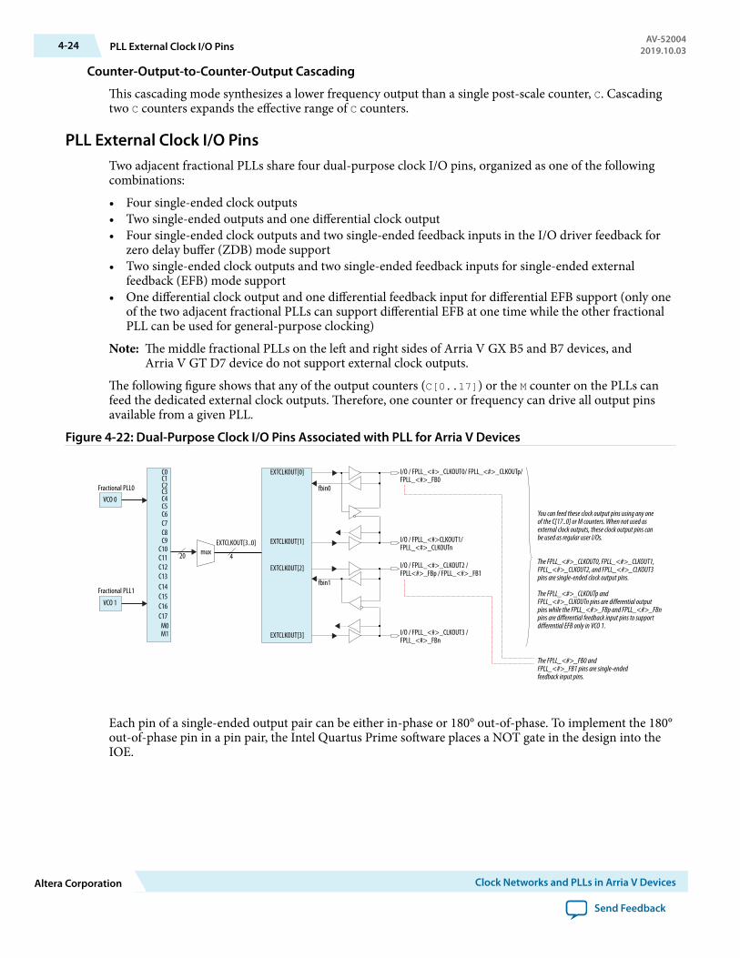
Counter-Output-to-Counter-Output Cascading
This cascading mode synthesizes a lower frequency output than a single post-scale counter, C. Cascadingtwo C counters expands the effective range of C counters.
PLL External Clock I/O PinsTwo adjacent fractional PLLs share four dual-purpose clock I/O pins, organized as one of the followingcombinations:
• Four single-ended clock outputs• Two single-ended outputs and one differential clock output• Four single-ended clock outputs and two single-ended feedback inputs in the I/O driver feedback for
zero delay buffer (ZDB) mode support• Two single-ended clock outputs and two single-ended feedback inputs for single-ended external
feedback (EFB) mode support• One differential clock output and one differential feedback input for differential EFB support (only one
of the two adjacent fractional PLLs can support differential EFB at one time while the other fractionalPLL can be used for general-purpose clocking)
Note: The middle fractional PLLs on the left and right sides of Arria V GX B5 and B7 devices, andArria V GT D7 device do not support external clock outputs.
The following figure shows that any of the output counters (C[0..17]) or the M counter on the PLLs canfeed the dedicated external clock outputs. Therefore, one counter or frequency can drive all output pinsavailable from a given PLL.
Figure 4-22: Dual-Purpose Clock I/O Pins Associated with PLL for Arria V Devices
VCO 0
VCO 1
C0C1C2C3C4C5C6C7C8C9
C10C11C12C13C14C15C16C17M0M1
I/O / FPLL_<#>_CLKOUT0/ FPLL_<#>_CLKOUTp/ FPLL_<#>_FB0
I/O / FPLL_<#>CLKOUT1/ FPLL_<#>_CLKOUTn
I/O / FPLL_<#>_CLKOUT2 / FPLL<#>_FBp / FPLL_<#>_FB1
fbin0
EXTCLKOUT[0]
EXTCLKOUT[1]
EXTCLKOUT[2]
EXTCLKOUT[3]
muxEXTCLKOUT[3..0]
Fractional PLL0
Fractional PLL1
I/O / FPLL_<#>_CLKOUT3 / FPLL_<#>_FBn
fbin1
420
You can feed these clock output pins using any one of the C[17..0] or M counters. When not used as external clock outputs, these clock output pins can be used as regular user I/Os.
The FPLL_<#>_CLKOUT0, FPLL_<#>_CLKOUT1, FPLL_<#>_CLKOUT2, and FPLL_<#>_CLKOUT3 pins are single-ended clock output pins.
The FPLL_<#>_CLKOUTp and FPLL_<#>_CLKOUTn pins are differential output pins while the FPLL_<#>_FBp and FPLL_<#>_FBn pins are differential feedback input pins to support differential EFB only in VCO 1.
The FPLL_<#>_FB0 and FPLL_<#>_FB1 pins are single-ended feedback input pins.
Each pin of a single-ended output pair can be either in-phase or 180° out-of-phase. To implement the 180°out-of-phase pin in a pin pair, the Intel Quartus Prime software places a NOT gate in the design into theIOE.
4-24 PLL External Clock I/O PinsAV-52004
2019.10.03
Altera Corporation Clock Networks and PLLs in Arria V Devices
Send Feedback

The clock output pin pairs support the following I/O standards:
• Same I/O standard for the pin pairs• LVDS• Differential high-speed transceiver logic (HSTL)• Differential SSTL
Arria V PLLs can drive out to any regular I/O pin through the GCLK or RCLK network. You can also usethe external clock output pins as user I/O pins if you do not require external PLL clocking.
Related Information
• I/O Standards Support in Arria V Devices on page 5-5Provides more information about I/O standards supported by the PLL clock input and output pins.
• Zero-Delay Buffer Mode on page 4-28• External Feedback Mode on page 4-30
PLL Control SignalsYou can use the areset signal to control PLL operation and resynchronization, and use the locked signalto observe the status of the PLL.
areset
The areset signal is the reset or resynchronization input for each PLL. The device input pins or internallogic can drive these input signals.
When areset is driven high, the PLL counters reset, clearing the PLL output and placing the PLL out-of-lock. The VCO is then set back to its nominal setting. When areset is driven low again, the PLL resynch‐ronizes to its input as it re-locks.
You must assert the areset signal every time the PLL loses lock to guarantee the correct phase relation‐ship between the PLL input and output clocks. You can set up the PLL to automatically reset (self-reset)after a loss-of-lock condition using the Intel Quartus Prime IP Catalog.
You must include the areset signal if either of the following conditions is true:
• PLL reconfiguration or clock switchover is enabled in the design• Phase relationships between the PLL input and output clocks must be maintained after a loss-of-lock
condition
Note: If the input clock to the PLL is not toggling or is unstable after power up, assert the areset signalafter the input clock is stable and within specifications.
locked
The locked signal output of the PLL indicates the following conditions:
• The PLL has locked onto the reference clock.• The PLL clock outputs are operating at the desired phase and frequency set in the IP Catalog.
The lock detection circuit provides a signal to the core logic. The signal indicates when the feedback clockhas locked onto the reference clock both in phase and frequency.
AV-520042019.10.03 PLL Control Signals 4-25
Clock Networks and PLLs in Arria V Devices Altera Corporation
Send Feedback

Clock Feedback ModesThis section describes the following clock feedback modes:
• Source synchronous• LVDS compensation• Direct• Normal compensation• ZDB• EFB
Each mode allows clock multiplication and division, phase shifting, and programmable duty cycle.
The input and output delays are fully compensated by a PLL only when using the dedicated clock inputpins associated with a given PLL as the clock source.
The input and output delays may not be fully compensated in the Intel Quartus Prime software for thefollowing conditions:
• When a GCLK or RCLK network drives the PLL• When the PLL is driven by a dedicated clock pin that is not associated with the PLL
For example, when you configure a PLL in ZDB mode, the PLL input is driven by an associated dedicatedclock input pin. In this configuration, a fully compensated clock path results in zero delay between theclock input and one of the clock outputs from the PLL. However, if the PLL input is fed by a non-dedicatedinput (using the GCLK network), the output clock may not be perfectly aligned with the input clock.
Source Synchronous Mode
If the data and clock arrive at the same time on the input pins, the same phase relationship is maintainedat the clock and data ports of any IOE input register. Data and clock signals at the IOE experience similarbuffer delays as long as you use the same I/O standard.
Altera recommends source synchronous mode for source synchronous data transfers.
Figure 4-23: Example of Phase Relationship Between Clock and Data in Source Synchronous Mode
Data Pin
PLL Reference Clockat the Input Pin
Data at the Register
Clock at the Register
4-26 Clock Feedback ModesAV-52004
2019.10.03
Altera Corporation Clock Networks and PLLs in Arria V Devices
Send Feedback

The source synchronous mode compensates for the delay of the clock network used and any difference inthe delay between the following two paths:
• Data pin to the IOE register input• Clock input pin to the PLL phase frequency detector (PFD) input
The Arria V PLL can compensate multiple pad-to-input-register paths, such as a data bus when it is set touse source synchronous compensation mode.
LVDS Compensation Mode
The purpose of LVDS compensation mode is to maintain the same data and clock timing relationship seenat the pins of the internal serializer/deserializer (SERDES) capture register, except that the clock is inverted(180° phase shift). Thus, LVDS compensation mode ideally compensates for the delay of the LVDS clocknetwork, including the difference in delay between the following two paths:
• Data pin-to-SERDES capture register• Clock input pin-to-SERDES capture register
The output counter must provide the 180° phase shift.
Figure 4-24: Example of Phase Relationship Between the Clock and Data in LVDS Compensation Mode
Data Pin
Data at the Register
Clock at the Register
PLL Reference Clock at the Input Pin
Direct Mode
In direct mode, the PLL does not compensate for any clock networks. This mode provides better jitterperformance because the clock feedback into the PFD passes through less circuitry. Both the PLL internal-and external-clock outputs are phase-shifted with respect to the PLL clock input.
AV-520042019.10.03 LVDS Compensation Mode 4-27
Clock Networks and PLLs in Arria V Devices Altera Corporation
Send Feedback

Figure 4-25: Example of Phase Relationship Between the PLL Clocks in Direct Mode
PLL ReferenceClock at the
Input Pin
PLL Clock at theRegister Clock Port
External PLLClock Outputs
Phase Aligned
The PLL clock outputs lag the PLL input clocks
depending on routing delays.
Normal Compensation Mode
An internal clock in normal compensation mode is phase-aligned to the input clock pin. The externalclock output pin has a phase delay relative to the clock input pin if connected in this mode. The IntelQuartus Prime Timing Analyzer reports any phase difference between the two. In normal compensationmode, the delay introduced by the GCLK or RCLK network is fully compensated.
Figure 4-26: Example of Phase Relationship Between the PLL Clocks in Normal Compensation Mode
PLL Clock at theRegister Clock Port
Dedicated PLLClock Outputs
Phase Aligned
PLL ReferenceClock at the Input Pin
The external clock output can lead or lag the PLL internal clock signals.
Zero-Delay Buffer Mode
In ZDB mode, the external clock output pin is phase-aligned with the clock input pin for zero delaythrough the device. This mode is supported on all Arria V PLLs.
4-28 Normal Compensation ModeAV-52004
2019.10.03
Altera Corporation Clock Networks and PLLs in Arria V Devices
Send Feedback
When using this mode, you must use the same I/O standard on the input clocks and clock outputs toguarantee clock alignment at the input and output pins. You cannot use differential I/O standards on thePLL clock input or output pins.
To ensure phase alignment between the clk pin and the external clock output (CLKOUT) pin in ZDB mode,instantiate a bidirectional I/O pin in the design. The bidirectional I/O pin serves as the feedback pathconnecting the fbout and fbin ports of the PLL. The bidirectional I/O pin must always be assigned asingle-ended I/O standard. The PLL uses this bidirectional I/O pin to mimic and compensate for theoutput delay from the clock output port of the PLL to the external clock output pin.
Note: To avoid signal reflection when using ZDB mode, do not place board traces on the bidirectional I/Opin.
Figure 4-27: ZDB Mode in Arria V PLLs
inclk÷N PFD VCO 0CP/LF
inclk÷N PFD VCO 1CP/LF
C0C1C2C3C4C5C6C7C8C9
C10C11C12C13
C14
C15
C16
C17
M0M1
EXTCLKOUT[1]
EXTCLKOUT[3]
EXTCLKOUT[0] fbout0
fbin0 BidirectionalI/O Pin
fbout1EXTCLKOUT[2]fbin1
420
Multiplexer
BidirectionalI/O Pin
AV-520042019.10.03 Zero-Delay Buffer Mode 4-29
Clock Networks and PLLs in Arria V Devices Altera Corporation
Send Feedback
Figure 4-28: Example of Phase Relationship Between the PLL Clocks in ZDB Mode
PLL Clock at theRegister Clock Port
Dedicated PLLClock Outputs
Phase Aligned
PLL Reference Clock at the Input Pin
The internal PLL clock output can lead or lag the external PLL clock
outputs.
Related InformationPLL External Clock I/O Pins on page 4-24Provides more information about PLL clock outputs.
External Feedback Mode
In EFB mode, the output of the M counter (fbout) feeds back to the PLL fbin input (using a trace on theboard) and becomes part of the feedback loop.
One of the dual-purpose external clock outputs becomes the fbin input pin in this mode. The externalfeedback input pin, fbin is phase-aligned with the clock input pin. Aligning these clocks allows you toremove clock delay and skew between devices.
When using EFB mode, you must use the same I/O standard on the input clock, feedback input, and clockoutputs.
4-30 External Feedback ModeAV-52004
2019.10.03
Altera Corporation Clock Networks and PLLs in Arria V Devices
Send Feedback

Figure 4-29: EFB Mode in Arria V Devices
inclk÷N PFD VCO 0CP/LF
inclk÷N PFD VCO 1CP/LF
C0C1C2C3C4C5C6C7C8C9
C10C11C12C13
C14C15C16C17M0M1
EXTCLKOUT[0]
EXTCLKOUT[1]
EXTCLKOUT[2]
EXTCLKOUT[3]
fbout0
fbin0
fbin[n]
fbout[n]
fbin1
fbout1
fbout[p]
fbin[p]
420Multiplexer
External board connection for one differential clock output and one differential feedback input for differential EFB support.
External board connection for two single-ended clock outputs and two single-ended feedback inputs for single-ended EFB support.
Only one of the two VCOs can support differential EFB mode at one time while you can use the other VCO for general purpose clocking.
ExternalBoard Trace
Figure 4-30: Example of Phase Relationship Between the PLL Clocks in EFB Mode
Dedicated PLL Clock Outputs
PLL Clock at the Register
Clock Port
fbin Clock Input Pin
Phase Aligned
PLL Reference Clock at the Input Pin
The PLL clock outputs can lead or lag the fbin
clock input.
Related InformationPLL External Clock I/O Pins on page 4-24Provides more information about PLL clock outputs.
AV-520042019.10.03 External Feedback Mode 4-31
Clock Networks and PLLs in Arria V Devices Altera Corporation
Send Feedback
Clock Multiplication and DivisionEach Arria V PLL provides clock synthesis for PLL output ports using the M/(N × C) scaling factors. Theinput clock is divided by a pre-scale factor, N, and is then multiplied by the M feedback factor. The controlloop drives the VCO to match fin × (M/N).
The Intel Quartus Prime software automatically chooses the appropriate scaling factors according to theinput frequency, multiplication, and division values entered into the ALTERA_PLL IP core.
VCO Post Divider
A VCO post divider is inserted after the VCO. When you enable the VCO post divider, the VCO postdivider divides the VCO frequency by two. When the VCO post divider is bypassed, the VCO frequencygoes to the output port without being divided by two.
Post-Scale Counter, C
Each output port has a unique post-scale counter, C, that divides down the output from the VCO postdivider. For multiple PLL outputs with different frequencies, the VCO is set to the least common multipleof the output frequencies that meets its frequency specifications. For example, if the output frequenciesrequired from one PLL are 33 and 66 MHz, the Intel Quartus Prime software sets the VCO to 660 MHz(the least common multiple of 33 and 66 MHz within the VCO range). Then the post-scale counters, C,scale down the VCO frequency for each output port.
Pre-Scale Counter, N and Multiply Counter, M
Each PLL has one pre-scale counter, N, and one multiply counter, M, with a range of 1 to 512 for both M andN. The N counter does not use duty-cycle control because the only purpose of this counter is to calculatefrequency division. The post-scale counters have a 50% duty cycle setting. The high- and low-count valuesfor each counter range from 1 to 256. The sum of the high- and low-count values chosen for a designselects the divide value for a given counter.
Delta-Sigma Modulator
The delta-sigma modulator (DSM) is used together with the M multiply counter to enable the PLL tooperate in fractional mode. The DSM dynamically changes the M counter divide value on a cycle to cyclebasis. The different M counter values allow the "average" M counter value to be a non-integer.
Fractional Mode
In fractional mode, the M counter divide value equals to the sum of the "clock high" count, "clock low"count, and the fractional value. The fractional value is equal to K/2^X, where K is an integer between 0 and(2^X – 1), and X = 8, 16, 24, or 32.
Integer Mode
For PLL operating in integer mode, M is an integer value and DSM is disabled.
Related InformationAltera Phase-Locked Loop (Altera PLL) IP Core User GuideProvides more information about PLL software support in the Quartus Prime software.
4-32 Clock Multiplication and DivisionAV-52004
2019.10.03
Altera Corporation Clock Networks and PLLs in Arria V Devices
Send Feedback
Programmable Phase ShiftThe programmable phase shift feature allows the PLLs to generate output clocks with a fixed phase offset.
The VCO frequency of the PLL determines the precision of the phase shift. The minimum phase shiftincrement is 1/8 of the VCO period. For example, if a PLL operates with a VCO frequency of 1000 MHz,phase shift steps of 125 ps are possible.
The Intel Quartus Prime software automatically adjusts the VCO frequency according to the user-specifiedphase shift values entered into the IP core.
Programmable Duty CycleThe programmable duty cycle allows PLLs to generate clock outputs with a variable duty cycle. This featureis supported on the PLL post-scale counters.
The duty-cycle setting is achieved by a low and high time-count setting for the post-scale counters. Todetermine the duty cycle choices, the Intel Quartus Prime software uses the frequency input and therequired multiply or divide rate.
The post-scale counter value determines the precision of the duty cycle. The precision is defined as 50%divided by the post-scale counter value. For example, if the C0 counter is 10, steps of 5% are possible forduty-cycle choices from 5% to 90%. If the PLL is in external feedback mode, set the duty cycle for thecounter driving the fbin pin to 50%.
Combining the programmable duty cycle with programmable phase shift allows the generation of precisenon-overlapping clocks.
Clock SwitchoverThe clock switchover feature allows the PLL to switch between two reference input clocks. Use this featurefor clock redundancy or for a dual-clock domain application where a system turns on the redundant clockif the previous clock stops running. The design can perform clock switchover automatically when the clockis no longer toggling or based on a user control signal, extswitch.
The following clock switchover modes are supported in Arria V PLLs:
• Automatic switchover—The clock sense circuit monitors the current reference clock. If the currentreference clock stops toggling, the reference clock automatically switches to inclk0 or inclk1 clock.
• Manual clock switchover—Clock switchover is controlled using the extswitch signal. When theextswitch signal goes from logic low to logic high, and stays high for at least three clock cycles, thereference clock to the PLL is switched from inclk0 to inclk1, or vice-versa.
• Automatic switchover with manual override—This mode combines automatic switchover and manualclock switchover. When the extswitch signal goes high, it overrides the automatic clock switchoverfunction.
Automatic Switchover
Arria V PLLs support a fully configurable clock switchover capability.
AV-520042019.10.03 Programmable Phase Shift 4-33
Clock Networks and PLLs in Arria V Devices Altera Corporation
Send Feedback
Figure 4-31: Automatic Clock Switchover Circuit Block Diagram
This figure shows a block diagram of the automatic switchover circuit built into the PLL.
ClockSense Switchover
State Machine
Clock SwitchControl Logic
N Counterinclk0inclk1
MultiplexerOut
clkbad[0]clkbad[1]
activeclock
extswitch
refclkfbclk
clksw
PFD
When the current reference clock is not present, the clock sense block automatically switches to thebackup clock for PLL reference. You can select a clock source as the backup clock by connecting it to theinclk1 port of the PLL in your design.
The clock switchover circuit sends out three status signals—clkbad[0], clkbad[1], and activeclock—from the PLL to implement a custom switchover circuit in the logic array.
In automatic switchover mode, the clkbad[0] and clkbad[1] signals indicate the status of the two clockinputs. When they are asserted, the clock sense block detects that the corresponding clock input hasstopped toggling. These two signals are not valid if the frequency difference between inclk0 and inclk1 isgreater than 20%.
The activeclock signal indicates which of the two clock inputs (inclk0 or inclk1) is being selected asthe reference clock to the PLL. When the frequency difference between the two clock inputs is more than20%, the activeclock signal is the only valid status signal.
Note: Glitches in the input clock may cause the frequency difference between the input clocks to be morethan 20%.
Use the switchover circuitry to automatically switch between inclk0 and inclk1 when the currentreference clock to the PLL stops toggling. You can switch back and forth between inclk0 and inclk1 anynumber of times when one of the two clocks fails and the other clock is available.
For example, in applications that require a redundant clock with the same frequency as the referenceclock, the switchover state machine generates a signal (clksw) that controls the multiplexer select input. Inthis case, inclk1 becomes the reference clock for the PLL.
When using automatic clock switchover mode, the following requirements must be satisfied:
• Both clock inputs must be running when the FPGA is configured.• The period of the two clock inputs can differ by no more than 20%.
4-34 Automatic SwitchoverAV-52004
2019.10.03
Altera Corporation Clock Networks and PLLs in Arria V Devices
Send Feedback

If the current clock input stops toggling while the other clock is also not toggling, switchover is notinitiated and the clkbad[0..1] signals are not valid. If both clock inputs are not the same frequency, buttheir period difference is within 20%, the clock sense block detects when a clock stops toggling. However,the PLL may lose lock after the switchover is completed and needs time to relock.
Note: Altera recommends resetting the PLL using the areset signal to maintain the phase relationshipsbetween the PLL input and output clocks when using clock switchover.
Figure 4-32: Automatic Switchover After Loss of Clock Detection
This figure shows an example waveform of the switchover feature in automatic switchover mode. In thisexample, the inclk0 signal is stuck low. After the inclk0 signal is stuck at low for approximately two clockcycles, the clock sense circuitry drives the clkbad[0] signal high. Since the reference clock signal is nottoggling, the switchover state machine controls the multiplexer through the extswitch signal to switch tothe backup clock, inclk1.
inclk0
inclk1
muxout
clkbad0
clkbad1
activeclock
Switchover is enabled on the falling edge of inclk0 or inclk1, depending on which clock is available. In this figure, switchover is enabled on the falling edge of inclk1.
Automatic Switchover with Manual Override
In automatic switchover with manual override mode, you can use the extswitch signal for user- orsystem-controlled switch conditions. You can use this mode for same-frequency switchover, or to switchbetween inputs of different frequencies.
For example, if inclk0 is 66 MHz and inclk1 is 200 MHz, you must control switchover using theextswitch signal. The automatic clock-sense circuitry cannot monitor clock input (inclk0 and inclk1)frequencies with a frequency difference of more than 100% (2×).
This feature is useful when the clock sources originate from multiple cards on the backplane, requiring asystem-controlled switchover between the frequencies of operation.
You must choose the backup clock frequency and set the M, N, C, and K counters so that the VCO operateswithin the recommended operating frequency range. The ALTERA_PLL IP Catalog notifies you if a givencombination of inclk0 and inclk1 frequencies cannot meet this requirement.
AV-520042019.10.03 Automatic Switchover with Manual Override 4-35
Clock Networks and PLLs in Arria V Devices Altera Corporation
Send Feedback
Figure 4-33: Clock Switchover Using the extswitch (Manual) Control
This figure shows a clock switchover waveform controlled by the extswitch signal. In this case, both clocksources are functional and inclk0 is selected as the reference clock; the extswitch signal goes high,which starts the switchover sequence. On the falling edge of inclk0, the counter’s reference clock, muxout,is gated off to prevent clock glitching. On the falling edge of inclk1, the reference clock multiplexerswitches from inclk0 to inclk1 as the PLL reference. The activeclock signal changes to indicate theclock which is currently feeding the PLL.
inclk0
inclk1
muxout
clkbad0
clkbad1
activeclock
extswitch
To initiate a manual clock switchover event, both inclk0 and inclk1 must be running when the extswitch signal goes high.
In automatic override with manual switchover mode, the activeclock signal mirrors the extswitchsignal. Since both clocks are still functional during the manual switch, neither clkbad signal goes high.Because the switchover circuit is positive-edge sensitive, the falling edge of the extswitch signal does notcause the circuit to switch back from inclk1 to inclk0. When the extswitch signal goes high again, theprocess repeats.
The extswitch signal and automatic switch work only if the clock being switched to is available. If theclock is not available, the state machine waits until the clock is available.
Related InformationAltera Phase-Locked Loop (Altera PLL) IP Core User GuideProvides more information about PLL software support in the Quartus Prime software.
Manual Clock Switchover
In manual clock switchover mode, the extswitch signal controls whether inclk0 or inclk1 is selected asthe input clock to the PLL. By default, inclk0 is selected.
A clock switchover event is initiated when the extswitch signal transitions from logic low to logic high,and being held high for at least three inclk cycles.
You must bring the extswitch signal back low again for PLL to re-gain lock. If you do not require anotherswitchover event, you can leave the extswitch signal in a logic low state.
Pulsing the extswitch signal high for at least three inclk cycles performs another switchover event.
4-36 Manual Clock SwitchoverAV-52004
2019.10.03
Altera Corporation Clock Networks and PLLs in Arria V Devices
Send Feedback
If inclk0 and inclk1 are different frequencies and are always running, the extswitch signal minimumhigh time must be greater than or equal to three of the slower frequency inclk0 and inclk1 cycles.
Figure 4-34: Manual Clock Switchover Circuitry in Arria V PLLs
Clock SwitchControl Logic
N Counter PFDinclk0inclk1
muxout refclk fbclk
extswitch
You can delay the clock switchover action by specifying the switchover delay in the ALTERA_PLL IP core.When you specify the switchover delay, the extswitch signal must be held high for at least three inclkcycles plus the number of the delay cycles that has been specified to initiate a clock switchover.
Related InformationAltera Phase-Locked Loop (Altera PLL) IP Core User GuideProvides more information about PLL software support in the Quartus Prime software.
Guidelines
When implementing clock switchover in Arria V PLLs, use the following guidelines:
• Automatic clock switchover requires that the inclk0 and inclk1 frequencies be within 20% of eachother. Failing to meet this requirement causes the clkbad[0] and clkbad[1] signals to not functionproperly.
• When using manual clock switchover, the difference between inclk0 and inclk1 can be more than100% (2×). However, differences in frequency, phase, or both, of the two clock sources will likely causethe PLL to lose lock. Resetting the PLL ensures that you maintain the correct phase relationshipsbetween the input and output clocks.
• Both inclk0 and inclk1 must be running when the extswitch signal goes high to initiate the manualclock switchover event. Failing to meet this requirement causes the clock switchover to not functionproperly.
• Applications that require a clock switchover feature and a small frequency drift must use a low-bandwidth PLL. When referencing input clock changes, the low-bandwidth PLL reacts more slowlythan a high-bandwidth PLL. When switchover happens, a low-bandwidth PLL propagates the stoppingof the clock to the output more slowly than a high-bandwidth PLL. However, be aware that the low-bandwidth PLL also increases lock time.
• After a switchover occurs, there may be a finite resynchronization period for the PLL to lock onto anew clock. The time it takes for the PLL to relock depends on the PLL configuration.
• The phase relationship between the input clock to the PLL and the output clock from the PLL isimportant in your design. Assert areset for at least 10 ns after performing a clock switchover. Wait forthe locked signal to go high and be stable before re-enabling the output clocks from the PLL.
• The VCO frequency gradually decreases when the current clock is lost and then increases as the VCOlocks on to the backup clock, as shown in the following figure.
AV-520042019.10.03 Guidelines 4-37
Clock Networks and PLLs in Arria V Devices Altera Corporation
Send Feedback
Figure 4-35: VCO Switchover Operating Frequency
∆ F vco
Primary Clock Stops Running
VCO Tracks Secondary Clock
Switchover Occurs
PLL Reconfiguration and Dynamic Phase ShiftFor more information about PLL reconfiguration and dynamic phase shifting, refer to AN661.
Related InformationAN 661: Implementing Fractional PLL Reconfiguration with Altera PLL and Altera PLL Reconfig IPCores
Clock Networks and PLLs in Arria V Devices Revision History
DocumentVersion
Changes
2019.04.26 • Corrected the signal name from clkswitch to extswitch.• Updated the description for the automatic switchover with manual override mode in the
Clock Switchover section.• Updated the description about the extswitch signal in the Manual Clock Switchover
section.
Date Version Changes
December2016
2016.12.09 Added a note to dedicated refclk pin in Fractional PLL High-Level BlockDiagram.
December2015
2015.12.21 Changed instances of Quartus II to Quartus Prime.
4-38 PLL Reconfiguration and Dynamic Phase ShiftAV-52004
2019.10.03
Altera Corporation Clock Networks and PLLs in Arria V Devices
Send Feedback

Date Version Changes
January 2015 2015.01.23 • Added a note pointing to FRACTIONALPLL_X183_Y63 and FRACTIO-NALPLL_X183_Y54 in PLL locations diagram for Arria V SX B3 andB5 Devices, and Arria V ST D3 and D5 Devices. Note: CLK10 andCLK11 clock pins feed into FRACTIONALPLL_X183_Y63 and FRACTIO-NALPLL_X183_Y54.
• PLL coordinates for Arria V GT C3 and C7 devices are finalized.Removed the notes that state the PLL coordinates will be finalized in afuture release of the Quartus II software from the PLL locationsdiagrams.
January 2014 2014.01.10 • Removed Preliminary tags for clock resources, clock input pinconnections to GCLK and RCLK networks, and PLL features tables.
• Updated clock resources table.• Added availability for RCLK[46..51] and RCLK[52..57] pins in
RCLK networks diagram.• Added notes to dedicated clock input pin connectivity to GCLK and
RCLK tables.• Added label for PLL strip in PLL locations diagrams.• Added descriptions for PLLs located in a strip.• Added PLL locations diagram for Arria V SX B3 and B5 devices, and
Arria V ST D3 and D5 devices.• Added information on PLL migration guidelines.• Updated VCO post-scale counter, K, to VCO post divider.• Added information on PLL cascading.• Added information on programmable phase shift.• Updated automatic clock switchover mode requirement.
AV-520042019.10.03 Clock Networks and PLLs in Arria V Devices Revision History 4-39
Clock Networks and PLLs in Arria V Devices Altera Corporation
Send Feedback
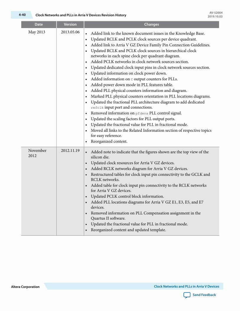
Date Version Changes
May 2013 2013.05.06 • Added link to the known document issues in the Knowledge Base.• Updated RCLK and PCLK clock sources per device quadrant.• Added link to Arria V GZ Device Family Pin Connection Guidelines.• Updated RCLK and PCLK clock sources in hierarchical clock
networks in each spine clock per quadrant diagram.• Added PCLK networks in clock network sources section.• Updated dedicated clock input pins in clock network sources section.• Updated information on clock power down.• Added information on C output counters for PLLs.• Added power down mode in PLL features table.• Added PLL physical counters information and diagram.• Marked PLL physical counters orientation in PLL locations diagrams.• Updated the fractional PLL architecture diagram to add dedicated
refclk input port and connections.• Removed information on pfdena PLL control signal.• Updated the scaling factors for PLL output ports.• Updated the fractional value for PLL in fractional mode.• Moved all links to the Related Information section of respective topics
for easy reference.• Reorganized content.
November2012
2012.11.19 • Added note to indicate that the figures shown are the top view of thesilicon die.
• Updated clock resources for Arria V GZ devices.• Added RCLK networks diagram for Arria V GZ devices.• Restructured tables for clock input pin connectivity to the GCLK and
RCLK networks.• Added table for clock input pin connectivity to the RCLK networks
for Arria V GZ devices.• Updated PCLK control block information.• Added PLL locations diagrams for Arria V GZ E1, E3, E5, and E7
devices.• Removed information on PLL Compensation assignment in the
Quartus II software.• Updated the fractional value for PLL in fractional mode.• Reorganized content and updated template.
4-40 Clock Networks and PLLs in Arria V Devices Revision HistoryAV-52004
2019.10.03
Altera Corporation Clock Networks and PLLs in Arria V Devices
Send Feedback

Date Version Changes
June 2012 2.0 • Restructured chapter.• Updated Figure 4–4, Figure 4–6, Figure 4–7, Figure 4–11, Figure 4–
12, Figure 4–13, Figure 4–14, Figure 4–15, Figure 4–16, Figure 4–18,and Figure 4–19.
• Updated Table 4–1, Table 4–2, Table 4–3, Table 4–4, and Table 4–5.• Added “Clock Regions”, “Clock Network Sources”, “Clock Output
Connections”, “Clock Enable Signals”, “PLL Control Signals”, “ClockMultiplication and Division”, “Programmable Duty Cycle”, “ClockSwitchover”, and “PLL Reconfiguration and Dynamic Phase Shift”.
November2011
1.1 Restructured chapter.
May 2011 1.0 Initial release.
AV-520042019.10.03 Clock Networks and PLLs in Arria V Devices Revision History 4-41
Clock Networks and PLLs in Arria V Devices Altera Corporation
Send Feedback

I/O Features in Arria V Devices 52019.10.03
AV-52005 Subscribe Send Feedback
This chapter provides details about the features of the Arria V I/O elements (IOEs) and how the IOEswork in compliance with current and emerging I/O standards and requirements.
The Arria V I/Os support the following features:
• Single-ended, non-voltage-referenced, and voltage-referenced I/O standards• Low-voltage differential signaling (LVDS), RSDS, mini-LVDS, HSTL, HSUL, and SSTL I/O standards• Serializer/deserializer (SERDES)• Programmable output current strength• Programmable slew rate• Programmable bus-hold• Programmable pull-up resistor• Programmable pre-emphasis• Programmable I/O delay• Programmable voltage output differential (VOD)• Open-drain output• On-chip series termination (RS OCT) with and without calibration• On-chip parallel termination (RT OCT)• On-chip differential termination (RD OCT)
Note: The information in this chapter is applicable to all Arria V variants, unless noted otherwise.
Related InformationArria V Device Handbook: Known IssuesLists the planned updates to the Arria V Device Handbook chapters.
I/O Resources Per Package for Arria V DevicesThe following package plan tables for the different Arria V variants list the maximum I/O resourcesavailable for each package.
Intel Corporation. All rights reserved. Intel, the Intel logo, Altera, Arria, Cyclone, Enpirion, MAX, Nios, Quartus and Stratix words and logos are trademarks ofIntel Corporation or its subsidiaries in the U.S. and/or other countries. Intel warrants performance of its FPGA and semiconductor products to currentspecifications in accordance with Intel's standard warranty, but reserves the right to make changes to any products and services at any time without notice.Intel assumes no responsibility or liability arising out of the application or use of any information, product, or service described herein except as expresslyagreed to in writing by Intel. Intel customers are advised to obtain the latest version of device specifications before relying on any published informationand before placing orders for products or services.*Other names and brands may be claimed as the property of others.
ISO9001:2015Registered
www.altera.com101 Innovation Drive, San Jose, CA 95134
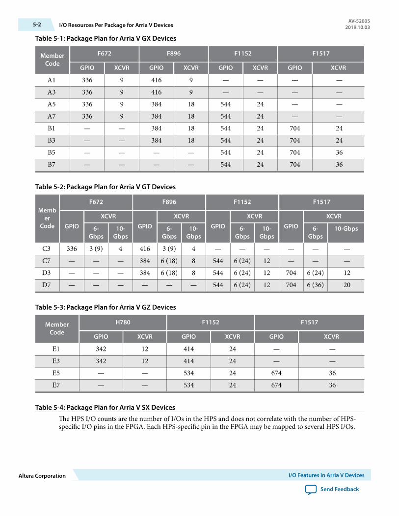
Table 5-1: Package Plan for Arria V GX Devices
MemberCode
F672 F896 F1152 F1517
GPIO XCVR GPIO XCVR GPIO XCVR GPIO XCVR
A1 336 9 416 9 — — — —A3 336 9 416 9 — — — —A5 336 9 384 18 544 24 — —A7 336 9 384 18 544 24 — —B1 — — 384 18 544 24 704 24B3 — — 384 18 544 24 704 24B5 — — — — 544 24 704 36B7 — — — — 544 24 704 36
Table 5-2: Package Plan for Arria V GT Devices
Member
Code
F672 F896 F1152 F1517
GPIO
XCVR
GPIO
XCVR
GPIO
XCVR
GPIO
XCVR
6-Gbps
10-Gbps
6-Gbps
10-Gbps
6-Gbps
10-Gbps
6-Gbps
10-Gbps
C3 336 3 (9) 4 416 3 (9) 4 — — — — — —C7 — — — 384 6 (18) 8 544 6 (24) 12 — — —D3 — — — 384 6 (18) 8 544 6 (24) 12 704 6 (24) 12D7 — — — — — — 544 6 (24) 12 704 6 (36) 20
Table 5-3: Package Plan for Arria V GZ Devices
MemberCode
H780 F1152 F1517
GPIO XCVR GPIO XCVR GPIO XCVR
E1 342 12 414 24 — —E3 342 12 414 24 — —E5 — — 534 24 674 36E7 — — 534 24 674 36
Table 5-4: Package Plan for Arria V SX Devices
The HPS I/O counts are the number of I/Os in the HPS and does not correlate with the number of HPS-specific I/O pins in the FPGA. Each HPS-specific pin in the FPGA may be mapped to several HPS I/Os.
5-2 I/O Resources Per Package for Arria V DevicesAV-52005
2019.10.03
Altera Corporation I/O Features in Arria V Devices
Send Feedback

MemberCode
F896 F1152 F1517
FPGAGPIO
HPS I/O XCVR FPGAGPIO
HPS I/O XCVR FPGAGPIO
HPS I/O XCVR
B3 250 208 12 385 208 18 540 208 30B5 250 208 12 385 208 18 540 208 30
Table 5-5: Package Plan for Arria V ST Devices
The HPS I/O counts are the number of I/Os in the HPS and does not correlate with the number of HPS-specific I/O pins in the FPGA. Each HPS-specific pin in the FPGA may be mapped to several HPS I/Os.
Member
Code
F896 F1152 F1517
FPGAGPIO
HPSI/O
XCVRFPGAGPIO
HPSI/O
XCVRFPGAGPIO
HPSI/O
XCVR
6 Gbps 10Gbps
6 Gbps 10Gbps
6 Gbps 10 Gbps
D3 250 208 12 6 385 208 18 8 540 208 30 16D5 250 208 12 6 385 208 18 8 540 208 30 16
For more information about each device variant, refer to the device overview.
Related Information
• True LVDS Buffers in Arria V Devices on page 6-5Lists the number of LVDS channels in each device package.
• Arria V Device Overview
AV-520052019.10.03 I/O Resources Per Package for Arria V Devices 5-3
I/O Features in Arria V Devices Altera Corporation
Send Feedback
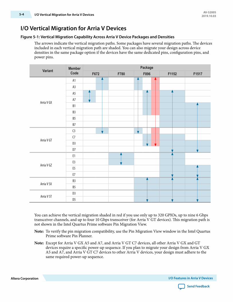
I/O Vertical Migration for Arria V DevicesFigure 5-1: Vertical Migration Capability Across Arria V Device Packages and Densities
The arrows indicate the vertical migration paths. Some packages have several migration paths. The devicesincluded in each vertical migration path are shaded. You can also migrate your design across devicedensities in the same package option if the devices have the same dedicated pins, configuration pins, andpower pins.
Variant Member Code
PackageF672 F780 F896 F1152 F1517
Arria V GX
A1
A3
A5
A7
B1
B3
B5
B7
Arria V GT
C3
C7
D3
D7
Arria V GZ
E1
E3
E5
E7
Arria V SXB3
B5
Arria V STD3
D5
You can achieve the vertical migration shaded in red if you use only up to 320 GPIOs, up to nine 6 Gbpstransceiver channels, and up to four 10 Gbps transceiver (for Arria V GT devices). This migration path isnot shown in the Intel Quartus Prime software Pin Migration View.
Note: To verify the pin migration compatibility, use the Pin Migration View window in the Intel QuartusPrime software Pin Planner.
Note: Except for Arria V GX A5 and A7, and Arria V GT C7 devices, all other Arria V GX and GTdevices require a specific power-up sequence. If you plan to migrate your design from Arria V GXA5 and A7, and Arria V GT C7 devices to other Arria V devices, your design must adhere to thesame required power-up sequence.
5-4 I/O Vertical Migration for Arria V DevicesAV-52005
2019.10.03
Altera Corporation I/O Features in Arria V Devices
Send Feedback
Related Information
• Arria V GX, GT, SX, and ST Power-Up Sequence on page 11-7• Verifying Pin Migration Compatibility on page 5-5• I/O Management chapter, Quartus II Handbook
Provides more information about vertical I/O migrations.• What is the difference between pin-to-pin compatibility and drop-in compatibility?
Verifying Pin Migration CompatibilityYou can use the Pin Migration View window in the Intel Quartus Prime software Pin Planner to assistyou in verifying whether your pin assignments migrate to a different device successfully. You can verticallymigrate to a device with a different density while using the same device package, or migrate betweenpackages with different densities and ball counts.
1. Open Assignments > Pin Planner and create pin assignments.2. If necessary, perform one of the following options to populate the Pin Planner with the node names in
the design:
• Analysis & Elaboration• Analysis & Synthesis• Fully compile the design
3. Then, on the menu, click View > Pin Migration View.4. To select or change migration devices:
a. Click Device to open the Device dialog box.b. Under Migration compatibility click Migration Devices.
5. To show more information about the pins:a. Right-click anywhere in the Pin Migration View window and select Show Columns.b. Then, click the pin feature you want to display.
6. If you want to view only the pins, in at least one migration device, that have a different feature than thecorresponding pin in the migration result, turn on Show migration differences.
7. Click Pin Finder to open the Pin Finder dialog box to find and highlight pins with specific function‐ality.If you want to view only the pins highlighted by the most recent query in the Pin Finder dialog box,turn on Show only highlighted pins.
8. To export the pin migration information to a Comma-Separated Value file (.csv), click Export.
Related Information
• I/O Vertical Migration for Arria V Devices on page 5-4• I/O Management chapter, Quartus II Handbook
Provides more information about vertical I/O migrations.
I/O Standards Support in Arria V DevicesThis section lists the I/O standards supported in the FPGA I/Os and HPS I/Os of Arria V devices, thetypical power supply values for each I/O standard, and the MultiVolt I/O interface feature.
AV-520052019.10.03 Verifying Pin Migration Compatibility 5-5
I/O Features in Arria V Devices Altera Corporation
Send Feedback

I/O Standards Support for FPGA I/O in Arria V Devices
Table 5-6: Supported I/O Standards in FPGA I/O for Arria V Devices
I/O Standard Device Variant Support Standard Support
3.3 V LVTTL/3.3 V LVCMOS All JESD8-B3.0 V LVTTL/3.0 V LVCMOS GX, GT, SX, and ST JESD8-B3.0 V PCI GX, GT, SX, and ST PCI Rev. 2.23.0 V PCI-X (10) GX, GT, SX, and ST PCI-X Rev. 1.02.5 V LVCMOS All JESD8-51.8 V LVCMOS All JESD8-71.5 V LVCMOS All JESD8-111.2 V LVCMOS All JESD8-12SSTL-2 Class I All JESD8-9BSSTL-2 Class II All JESD8-9BSSTL-18 Class I All JESD8-15SSTL-18 Class II All JESD8-15SSTL-15 Class I All —SSTL-15 Class II All —1.8 V HSTL Class I All JESD8-61.8 V HSTL Class II All JESD8-61.5 V HSTL Class I All JESD8-61.5 V HSTL Class II All JESD8-61.2 V HSTL Class I All JESD8-16A1.2 V HSTL Class II All JESD8-16ADifferential SSTL-2 Class I All JESD8-9BDifferential SSTL-2 Class II All JESD8-9BDifferential SSTL-18 Class I All JESD8-15Differential SSTL-18 Class II All JESD8-15Differential SSTL-15 Class I All —Differential SSTL-15 Class II All —Differential 1.8 V HSTL Class I All JESD8-6Differential 1.8 V HSTL Class II All JESD8-6Differential 1.5 V HSTL Class I All JESD8-6
(10) PCI-X does not meet the PCI-X I–V curve requirement at the linear region.
5-6 I/O Standards Support for FPGA I/O in Arria V DevicesAV-52005
2019.10.03
Altera Corporation I/O Features in Arria V Devices
Send Feedback

I/O Standard Device Variant Support Standard Support
Differential 1.5 V HSTL Class II All JESD8-6Differential 1.2 V HSTL Class I All JESD8-16ADifferential 1.2 V HSTL Class II All JESD8-16ALVDS All ANSI/TIA/EIA-644RSDS(11) All —Mini-LVDS(12) All —LVPECL All —SSTL-15 All JESD79-3DSSTL-135 All —SSTL-125 All —SSTL-12 GZ only —HSUL-12 All —Differential SSTL-15 All JESD79-3DDifferential SSTL-135 All —Differential SSTL-125 All —Differential SSTL-12 GZ only —Differential HSUL-12 All —
I/O Standards Support for HPS I/O in Arria V Devices
Table 5-7: Supported I/O Standards in HPS I/O for Arria V SX and ST Devices
I/O Standard Standard Support HPS Column I/O HPS Row I/O
3.3 V LVTTL/3.3 V LVCMOS JESD8-B Yes —3.0 V LVTTL/3.0 V LVCMOS JESD8-B Yes —2.5 V LVCMOS JESD8-5 Yes —1.8 V LVCMOS JESD8-7 Yes Yes1.5 V LVCMOS JESD8-11 Yes —SSTL-18 Class I JESD8-15 — YesSSTL-18 Class II JESD8-15 — YesSSTL-15 Class I — — Yes
(11) The Arria V devices support true RSDS output standard with data rates of up to 360 Mbps (for Arria V GX/GT/SX/ST) and 230 Mbps (for Arria V GZ) using true LVDS output buffer types on all I/O banks.
(12) The Arria V devices support true mini-LVDS output standard with data rates of up to 400 Mbps (for Arria VGX/GT/SX/ST) and 340 Mbps (for Arria V GZ) using true LVDS output buffer types on all I/O banks.
AV-520052019.10.03 I/O Standards Support for HPS I/O in Arria V Devices 5-7
I/O Features in Arria V Devices Altera Corporation
Send Feedback
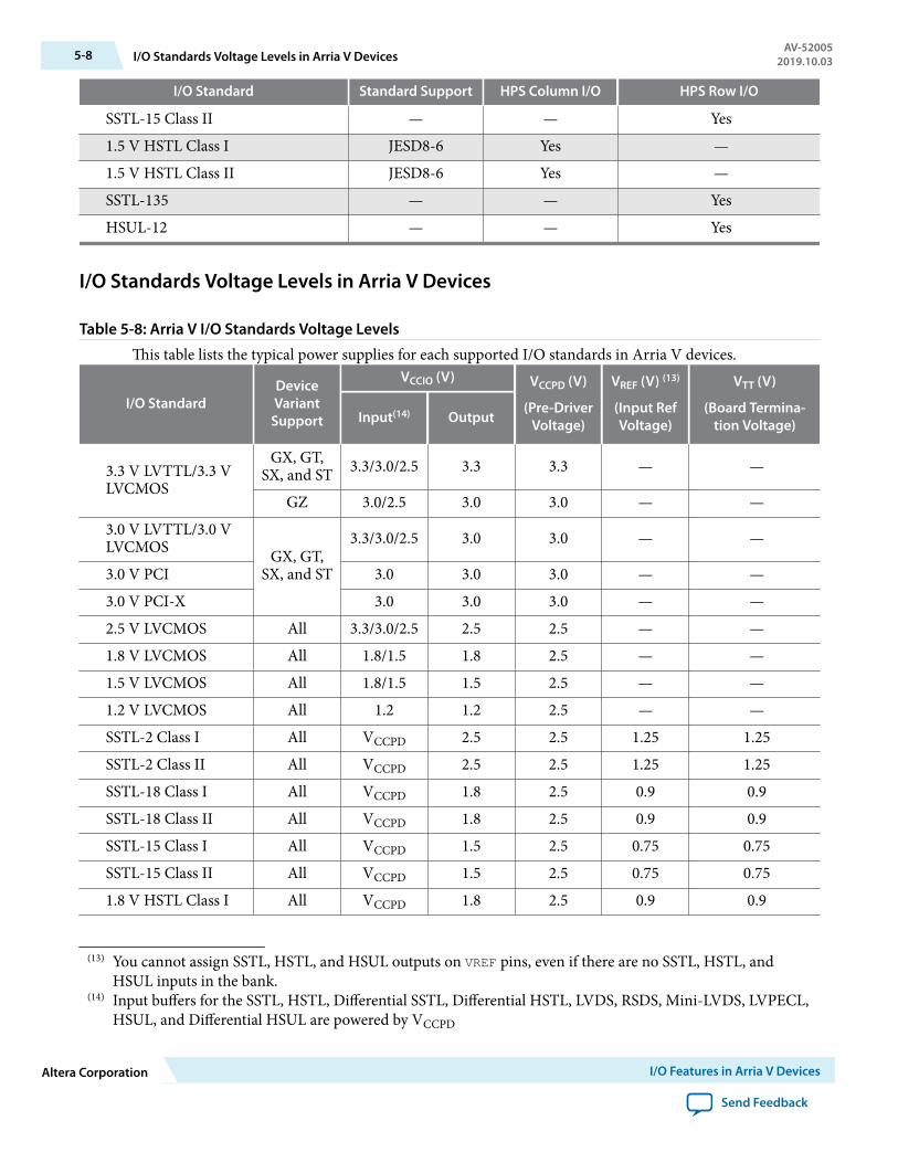
I/O Standard Standard Support HPS Column I/O HPS Row I/O
SSTL-15 Class II — — Yes1.5 V HSTL Class I JESD8-6 Yes —1.5 V HSTL Class II JESD8-6 Yes —SSTL-135 — — YesHSUL-12 — — Yes
I/O Standards Voltage Levels in Arria V Devices
Table 5-8: Arria V I/O Standards Voltage Levels
This table lists the typical power supplies for each supported I/O standards in Arria V devices.
I/O StandardDeviceVariant
Support
VCCIO (V) VCCPD (V)
(Pre-DriverVoltage)
VREF (V) (13)
(Input RefVoltage)
VTT (V)
(Board Termina‐tion Voltage)Input(14) Output
3.3 V LVTTL/3.3 VLVCMOS
GX, GT,SX, and ST 3.3/3.0/2.5 3.3 3.3 — —
GZ 3.0/2.5 3.0 3.0 — —3.0 V LVTTL/3.0 VLVCMOS GX, GT,
SX, and ST
3.3/3.0/2.5 3.0 3.0 — —
3.0 V PCI 3.0 3.0 3.0 — —3.0 V PCI-X 3.0 3.0 3.0 — —2.5 V LVCMOS All 3.3/3.0/2.5 2.5 2.5 — —1.8 V LVCMOS All 1.8/1.5 1.8 2.5 — —1.5 V LVCMOS All 1.8/1.5 1.5 2.5 — —1.2 V LVCMOS All 1.2 1.2 2.5 — —SSTL-2 Class I All VCCPD 2.5 2.5 1.25 1.25SSTL-2 Class II All VCCPD 2.5 2.5 1.25 1.25SSTL-18 Class I All VCCPD 1.8 2.5 0.9 0.9SSTL-18 Class II All VCCPD 1.8 2.5 0.9 0.9SSTL-15 Class I All VCCPD 1.5 2.5 0.75 0.75SSTL-15 Class II All VCCPD 1.5 2.5 0.75 0.751.8 V HSTL Class I All VCCPD 1.8 2.5 0.9 0.9
(13) You cannot assign SSTL, HSTL, and HSUL outputs on VREF pins, even if there are no SSTL, HSTL, andHSUL inputs in the bank.
(14) Input buffers for the SSTL, HSTL, Differential SSTL, Differential HSTL, LVDS, RSDS, Mini-LVDS, LVPECL,HSUL, and Differential HSUL are powered by VCCPD
5-8 I/O Standards Voltage Levels in Arria V DevicesAV-52005
2019.10.03
Altera Corporation I/O Features in Arria V Devices
Send Feedback
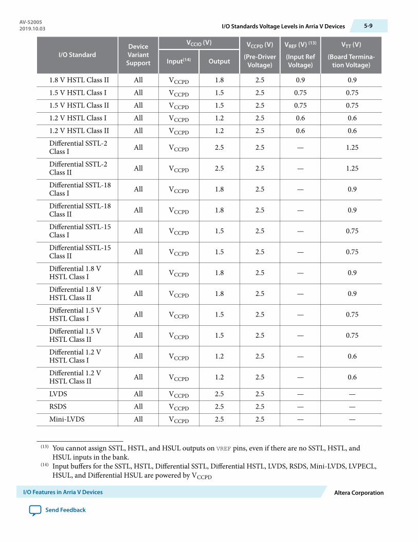
I/O StandardDeviceVariant
Support
VCCIO (V) VCCPD (V)
(Pre-DriverVoltage)
VREF (V) (13)
(Input RefVoltage)
VTT (V)
(Board Termina‐tion Voltage)Input(14) Output
1.8 V HSTL Class II All VCCPD 1.8 2.5 0.9 0.91.5 V HSTL Class I All VCCPD 1.5 2.5 0.75 0.751.5 V HSTL Class II All VCCPD 1.5 2.5 0.75 0.751.2 V HSTL Class I All VCCPD 1.2 2.5 0.6 0.61.2 V HSTL Class II All VCCPD 1.2 2.5 0.6 0.6Differential SSTL-2Class I All VCCPD 2.5 2.5 — 1.25
Differential SSTL-2Class II All VCCPD 2.5 2.5 — 1.25
Differential SSTL-18Class I All VCCPD 1.8 2.5 — 0.9
Differential SSTL-18Class II All VCCPD 1.8 2.5 — 0.9
Differential SSTL-15Class I All VCCPD 1.5 2.5 — 0.75
Differential SSTL-15Class II All VCCPD 1.5 2.5 — 0.75
Differential 1.8 VHSTL Class I All VCCPD 1.8 2.5 — 0.9
Differential 1.8 VHSTL Class II All VCCPD 1.8 2.5 — 0.9
Differential 1.5 VHSTL Class I All VCCPD 1.5 2.5 — 0.75
Differential 1.5 VHSTL Class II All VCCPD 1.5 2.5 — 0.75
Differential 1.2 VHSTL Class I All VCCPD 1.2 2.5 — 0.6
Differential 1.2 VHSTL Class II All VCCPD 1.2 2.5 — 0.6
LVDS All VCCPD 2.5 2.5 — —RSDS All VCCPD 2.5 2.5 — —Mini-LVDS All VCCPD 2.5 2.5 — —
(13) You cannot assign SSTL, HSTL, and HSUL outputs on VREF pins, even if there are no SSTL, HSTL, andHSUL inputs in the bank.
(14) Input buffers for the SSTL, HSTL, Differential SSTL, Differential HSTL, LVDS, RSDS, Mini-LVDS, LVPECL,HSUL, and Differential HSUL are powered by VCCPD
AV-520052019.10.03 I/O Standards Voltage Levels in Arria V Devices 5-9
I/O Features in Arria V Devices Altera Corporation
Send Feedback

I/O StandardDeviceVariant
Support
VCCIO (V) VCCPD (V)
(Pre-DriverVoltage)
VREF (V) (13)
(Input RefVoltage)
VTT (V)
(Board Termina‐tion Voltage)Input(14) Output
LVPECL (Differentialclock input only) All VCCPD — 2.5 — —
SSTL-15 All VCCPD 1.5 2.5 0.75
Typically does notrequire boardtermination
SSTL-135 All VCCPD 1.35 2.5 0.675SSTL-125 All VCCPD 1.25 2.5 0.625SSTL-12 GZ only VCCPD 1.2 2.5 0.6HSUL-12 All VCCPD 1.2 2.5 0.6Differential SSTL-15 All VCCPD 1.5 2.5 —
Typically does notrequire boardtermination
Differential SSTL-135 All VCCPD 1.35 2.5 —Differential SSTL-125 All VCCPD 1.25 2.5 —Differential SSTL-12 GZ only VCCPD 1.2 2.5 —Differential HSUL-12 All VCCPD 1.2 2.5 —
Related InformationGuideline: Observe Device Absolute Maximum Rating for 3.3 V Interfacing on page 5-13Provides more information about the 3.3 V LVTTL/LVCMOS I/O standard supported in Arria V GZdevices.
MultiVolt I/O Interface in Arria V DevicesThe MultiVolt I/O interface feature allows Arria V devices in all packages to interface with systems ofdifferent supply voltages.
Table 5-9: MultiVolt I/O Support in Arria V Devices
VCCIO (V) Device VariantSupport
VCCPD (V) (14) Input Signal (V) Output Signal (V)
1.2 All 2.5 1.2 1.21.25 All 2.5 1.25 1.251.35 All 2.5 1.35 1.351.5 All 2.5 1.5, 1.8 1.51.8 All 2.5 1.5, 1.8 1.82.5 All 2.5 2.5, 3.0, 3.3 2.5
(13) You cannot assign SSTL, HSTL, and HSUL outputs on VREF pins, even if there are no SSTL, HSTL, andHSUL inputs in the bank.
(14) Input buffers for the SSTL, HSTL, Differential SSTL, Differential HSTL, LVDS, RSDS, Mini-LVDS, LVPECL,HSUL, and Differential HSUL are powered by VCCPD
5-10 MultiVolt I/O Interface in Arria V DevicesAV-52005
2019.10.03
Altera Corporation I/O Features in Arria V Devices
Send Feedback

VCCIO (V) Device VariantSupport
VCCPD (V) (14) Input Signal (V) Output Signal (V)
3.0GX, GT, SX, and
ST3.0 2.5, 3.0, 3.3 3.0
GZ 3.0 2.5, 3.0, 3.3 3.0, 3.33.3 GX, GT, SX, and
ST3.3 2.5, 3.0, 3.3 3.3
The pin current may be slightly higher than the default value. Verify that the VOL maximum and VOHminimum voltages of the driving device do not violate the applicable VIL maximum and VIH minimumvoltage specifications of the Arria V device.
The VCCPD power pins must be connected to a 2.5 V, 3.0 V, or 3.3 V power supply. Using these power pinsto supply the pre-driver power to the output buffers increases the performance of the output pins.
Note: If the input signal is 3.0 V or 3.3 V, Altera recommends that you use a clamping diode on the I/Opins. Use the on-chip clamping diode for the Arria V GX, GT, SX, and ST devices, and an externalclamping diode for the Arria V GZ devices.
I/O Design Guidelines for Arria V DevicesThere are several considerations that require your attention to ensure the success of your designs. Unlessnoted otherwise, these design guidelines apply to all variants of this device family.
Mixing Voltage-Referenced and Non-Voltage-Referenced I/O StandardsEach I/O bank can simultaneously support multiple I/O standards. The following sections provideguidelines for mixing non-voltage-referenced and voltage-referenced I/O standards in the devices.
Non-Voltage-Referenced I/O Standards
Each Arria V I/O bank has its own VCCIO pins and supports only one VCCIO of 1.2, 1.25, 1.35, 1.5, 1.8, 2.5,3.0, or 3.3 V(15). An I/O bank can simultaneously support any number of input signals with different I/Ostandard assignments if the I/O standards support the VCCIO level of the I/O bank.
For output signals, a single I/O bank supports non-voltage-referenced output signals that drive at the samevoltage as VCCIO. Because an I/O bank can only have one VCCIO value, it can only drive out the value fornon-voltage-referenced signals.
For example, an I/O bank with a 2.5 V VCCIO setting can support 2.5 V, 3.0 V and 3.3 V inputs butsupports only 2.5 V output.
(15) Arria V GZ devices do not support 3.3 V
AV-520052019.10.03 I/O Design Guidelines for Arria V Devices 5-11
I/O Features in Arria V Devices Altera Corporation
Send Feedback
Voltage-Referenced I/O Standards
To accommodate voltage-referenced I/O standards:
• Each Arria V GX, GT, SX, or ST I/O bank contains a dedicated VREF pin.• Each Arria V GZ I/O bank supports multiple dedicated VREF pins feeding a common VREF bus.• Each bank can have only a single VCCIO voltage level and a single voltage reference (VREF) level.
An I/O bank featuring single-ended or differential standards can support different voltage-referencedstandards if the VCCIO and VREF are the same levels.
For performance reasons, voltage-referenced input standards use their own VCCPD level as the powersource. This feature allows you to place voltage-referenced input signals in an I/O bank with a VCCIO of2.5 V or below. For example, you can place HSTL-15 input pins in an I/O bank with 2.5 V VCCIO.However, the voltage-referenced input with RT OCT enabled requires the VCCIO of the I/O bank to matchthe voltage of the input standard. RT OCT cannot be supported for the HSTL-15 I/O standard when VCCIOis 2.5 V.
Voltage-referenced bidirectional and output signals must be the same as the VCCIO voltage of the I/O bank.For example, you can place only SSTL-2 output pins in an I/O bank with a 2.5 V VCCIO.
Mixing Voltage-Referenced and Non-Voltage Referenced I/O Standards
An I/O bank can support voltage-referenced and non-voltage-referenced pins by applying each of the rulesets individually.
Examples:
• An I/O bank can support SSTL-18 inputs and outputs, and 1.8 V inputs and outputs with a 1.8 V VCCIOand a 0.9 V VREF.
• An I/O bank can support 1.5 V standards, 1.8 V inputs (but not outputs), and 1.5 V HSTL I/Ostandards with a 1.5 V VCCIO and 0.75 V VREF.
Guideline: Use the Same VCCPD for All I/O Banks in a GroupOne VCCPD is shared in a group of I/O banks. If one I/O bank in a group uses 3.0 V VCCPD, other I/Obanks in the same group must also use 3.0 V VCCPD.
The I/O banks with the same bank number form a group. For example, I/O banks 8A, 8B, 8C, and 8Dform a group and share the same VCCPD. This sharing is applicable to all I/O banks, with the followingexceptions:
• Arria V GX and GT devices—No VCCPD sharing in bank 4A and 7A. Each of these I/O banks has theirown individual VCCPD.
• Arria V SX and ST devices—No VCCPD sharing in bank 4A. In these devices, banks 6A, 6B, and 7Athrough 7E are HPS I/O banks.
• Arria V GZ devices—No VCCPD sharing across banks 3A, 3B, 3C, and 3D. Banks 3A and 3B form agroup with one VCCPD while bank 3C (if available) and 3D form another group with its own VCCPD.
For the Arria V GZ devices, if you are using an output or bidirectional pin with the 3.3 V LVTTL or 3.3 VLVCMOS I/O standard, you must adhere to this restriction manually with location assignments.
For more information about the I/O banks available in each device package, refer to the related informa‐tion.
5-12 Voltage-Referenced I/O StandardsAV-52005
2019.10.03
Altera Corporation I/O Features in Arria V Devices
Send Feedback
Related Information
• Modular I/O Banks for Arria V GX Devices on page 5-18• Modular I/O Banks for Arria V GT Devices on page 5-20• Modular I/O Banks for Arria V GZ Devices on page 5-21• Modular I/O Banks for Arria V SX Devices on page 5-22• Modular I/O Banks for Arria V ST Devices on page 5-23
Guideline: Ensure Compatible VCCIO and VCCPD Voltage in the Same BankWhen planning I/O bank usage for Arria V GX, GT, SX, and ST devices, you must ensure the VCCIOvoltage is compatible with the VCCPD voltage of the same bank. Some banks may share the same VCCPDpower pin. This limits the possible VCCIO voltages that can be used on banks that share VCCPD power pins.
Examples:
• VCCPD4BCD is connected to 2.5 V—VCCIO pins for banks 4B, 4C, and 4D can be connected 1.2 V, 1.25 V,1.35 V, 1.5 V, 1.8 V, or 2.5 V.
• VCCPD4BCD is connected to 3.0 V—VCCIO pins for banks 4B, 4C, and 4D must be connected to 3.0 V.
Guideline: VREF Pin RestrictionsFor the Arria V GX, GT, SX, and ST devices, consider the following VREF pins guidelines:
• You cannot assign shared VREF pins as LVDS or external memory interface pins.• SSTL, HSTL, and HSUL I/O standards do not support shared VREF pins. For example, if a particular
B1p or B1n pin is a shared VREF pin, the corresponding B1p/B1n pin pair do not have LVDS transmittersupport.
• Shared VREF pins will have reduced performance when used as normal I/Os.• You must perform signal integrity analysis using your board design when using a shared VREF pin to
determine the FMAX for your system.
For more information about pin capacitance of the VREF pins, refer to the device datasheet.
Related Information
• Arria V GX, GT, SX, and ST Device Datasheet• Arria V GZ Device Datasheet
Guideline: Observe Device Absolute Maximum Rating for 3.3 V InterfacingTo ensure device reliability and proper operation when you use the device for 3.3 V I/O interfacing, do notviolate the absolute maximum ratings of the device. For more information about absolute maximumrating and maximum allowed overshoot during transitions, refer to the device datasheet.
Tip: Perform IBIS or SPICE simulations to make sure the overshoot and undershoot voltages are withinthe specifications.
Transmitter Application
If you use the Arria V device as a transmitter, use slow slew rate and series termination to limit theovershoot and undershoot at the I/O pins. Transmission line effects that cause large voltage deviations atthe receiver are associated with an impedance mismatch between the driver and the transmission lines. By
AV-520052019.10.03 Guideline: Ensure Compatible VCCIO and VCCPD Voltage in the Same Bank 5-13
I/O Features in Arria V Devices Altera Corporation
Send Feedback
matching the impedance of the driver to the characteristic impedance of the transmission line, you cansignificantly reduce overshoot voltage. You can use a series termination resistor placed physically close tothe driver to match the total driver impedance to the transmission line impedance.
Receiver Application
If you use the Arria V device as a receiver, to limit the overshoot and undershoot voltage at the I/O pins:
• Arria V GX, GT, SX, or ST—use the on-chip clamping diode.• Arria V GZ device—use an off-chip clamping diode.
The 3.3 V I/O standard is supported using the bank supply voltage (VCCIO) at 3.0 V and a VCCPD voltage of3.0 V. In this method, the clamping diode can sufficiently clamp overshoot voltage to within the DC andAC input voltage specifications. The clamped voltage is expressed as the sum of the VCCIO and the diodeforward voltage.
Related Information
• Arria V GX, GT, SX, and ST Device Datasheet• Arria V GZ Device Datasheet
Guideline: Use PLL Integer Mode for LVDS ApplicationsFor LVDS applications, you must use the phase-locked loops (PLLs) in integer PLL mode.
Related InformationGuideline: Use PLLs in Integer PLL Mode for LVDS on page 6-8
Guideline: Pin Placement for General Purpose High-Speed SignalsFor general purpose high-speed signals faster than 200 MHz, follow these guidelines to ensure I/O timingclosure.
• Avoid using HMC DQ pins as the input pin.• Avoid using HMC DQ and command pins as the output pin.
I/O signals that use the hard memory controller pins are routed through the HMCPHY_RE routing elements.These routing elements have a higher routing delay compared to other I/O pins. To identify the hardmemory controller pins for your Arria V device and package, refer to the relevant pin-out files.
Related InformationArria V Device Pin-Out FilesProvides the pin-out files for each Arria V device package.
I/O Banks Locations in Arria V DevicesThe number of Arria V I/O banks in a particular device depends on the device density.
5-14 Guideline: Use PLL Integer Mode for LVDS ApplicationsAV-52005
2019.10.03
Altera Corporation I/O Features in Arria V Devices
Send Feedback
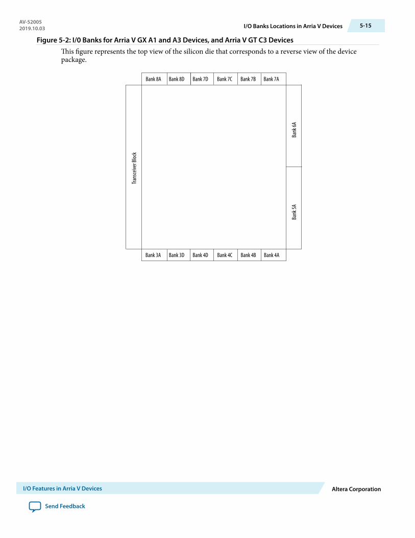
Figure 5-2: I/0 Banks for Arria V GX A1 and A3 Devices, and Arria V GT C3 DevicesThis figure represents the top view of the silicon die that corresponds to a reverse view of the devicepackage.
Bank
5ABa
nk 6A
Bank 8A Bank 8D
Trans
ceive
r Bloc
k
Bank 7B Bank 7ABank 7CBank 7D
Bank 4ABank 4BBank 3A Bank 3D Bank 4CBank 4D
AV-520052019.10.03 I/O Banks Locations in Arria V Devices 5-15
I/O Features in Arria V Devices Altera Corporation
Send Feedback
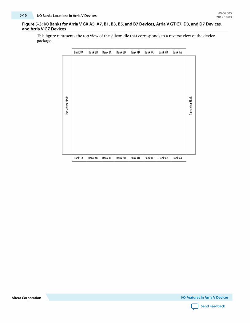
Figure 5-3: I/0 Banks for Arria V GX A5, A7, B1, B3, B5, and B7 Devices, Arria V GT C7, D3, and D7 Devices,and Arria V GZ Devices
This figure represents the top view of the silicon die that corresponds to a reverse view of the devicepackage.
Bank 8A
Trans
ceive
r Bloc
k
Bank 7B Bank 7ABank 7CBank 7DBank 8C Bank 8DBank 8B
Bank 4ABank 4BBank 3BBank 3A Bank 3C Bank 3D Bank 4CBank 4D
Trans
ceive
r Bloc
k
5-16 I/O Banks Locations in Arria V DevicesAV-52005
2019.10.03
Altera Corporation I/O Features in Arria V Devices
Send Feedback

Figure 5-4: I/0 Banks for Arria V SX B3 and B5 Devices, and Arria V ST D3 and D5 DevicesThis figure represents the top view of the silicon die that corresponds to a reverse view of the devicepackage.
Bank 8A
Trans
ceive
r Bloc
k
Bank 8C Bank 8D Bank 7GBank 8B
Bank 4ABank 4BBank 3BBank 3A Bank 3C Bank 3D Bank 4CBank 4D
Trans
ceive
r Bloc
k
HPS Column I/O
HPS R
ow I/
O
HPS Core
Related Information
• Modular I/O Banks for Arria V GX Devices on page 5-18• Modular I/O Banks for Arria V GT Devices on page 5-20• Modular I/O Banks for Arria V GZ Devices on page 5-21• Modular I/O Banks for Arria V SX Devices on page 5-22• Modular I/O Banks for Arria V ST Devices on page 5-23
I/O Banks Groups in Arria V DevicesThe I/O pins in Arria V devices are arranged in groups called modular I/O banks:
• Modular I/O banks have independent power supplies that allow each bank to support different I/Ostandards.
• Each modular I/O bank can support multiple I/O standards that use the same VCCIO and VCCPDvoltages.
AV-520052019.10.03 I/O Banks Groups in Arria V Devices 5-17
I/O Features in Arria V Devices Altera Corporation
Send Feedback
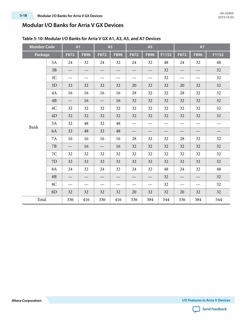
Modular I/O Banks for Arria V GX Devices
Table 5-10: Modular I/O Banks for Arria V GX A1, A3, A5, and A7 Devices
Member Code A1 A3 A5 A7
Package F672 F896 F672 F896 F672 F896 F1152 F672 F896 F1152
Bank
3A 24 32 24 32 24 32 48 24 32 483B — — — — — — 32 — — 323C — — — — — — 32 — — 323D 32 32 32 32 20 32 32 20 32 324A 16 16 16 16 28 32 32 28 32 324B — 16 — 16 32 32 32 32 32 324C 32 32 32 32 32 32 32 32 32 324D 32 32 32 32 32 32 32 32 32 325A 32 48 32 48 — — — — — —6A 32 48 32 48 — — — — — —7A 16 16 16 16 28 32 32 28 32 327B — 16 — 16 32 32 32 32 32 327C 32 32 32 32 32 32 32 32 32 327D 32 32 32 32 32 32 32 32 32 328A 24 32 24 32 24 32 48 24 32 488B — — — — — — 32 — — 328C — — — — — — 32 — — 328D 32 32 32 32 20 32 32 20 32 32
Total 336 416 336 416 336 384 544 336 384 544
5-18 Modular I/O Banks for Arria V GX DevicesAV-52005
2019.10.03
Altera Corporation I/O Features in Arria V Devices
Send Feedback

Table 5-11: Modular I/O Banks for Arria V GX B1, B3, B5, and B7 Devices
Member Code B1 B3 B5 B7
Package F896 F1152 F1517 F896 F1152 F1517 F1152 F1517 F1152 F1517
Bank
3A 32 48 48 32 48 48 48 48 48 483B — 32 32 — 32 32 32 32 32 323C — 32 48 — 32 48 32 48 32 483D 32 32 48 32 32 48 32 48 32 484A 32 32 48 32 32 48 32 48 32 484B 32 32 48 32 32 48 32 48 32 484C 32 32 32 32 32 32 32 32 32 324D 32 32 48 32 32 48 32 48 32 487A 32 32 48 32 32 48 32 48 32 487B 32 32 48 32 32 48 32 48 32 487C 32 32 32 32 32 32 32 32 32 327D 32 32 48 32 32 48 32 48 32 488A 32 48 48 32 48 48 48 48 48 488B — 32 32 — 32 32 32 32 32 328C — 32 48 — 32 48 32 48 32 488D 32 32 48 32 32 48 32 48 32 48
Total 384 544 704 384 544 704 544 704 544 704
Related Information
• I/O Banks Locations in Arria V Devices on page 5-14• Guideline: Use the Same VCCPD for All I/O Banks in a Group on page 5-12
Provides guidelines about VCCPD and I/O banks groups.
AV-520052019.10.03 Modular I/O Banks for Arria V GX Devices 5-19
I/O Features in Arria V Devices Altera Corporation
Send Feedback

Modular I/O Banks for Arria V GT Devices
Table 5-12: Modular I/O Banks for Arria V GT Devices
Member Code C3 C7 D3 D7
Package F672 F896 F896 F1152 F896 F1152 F1517 F1152 F1517
Bank
3A 24 32 32 48 32 48 48 48 483B — — — 32 — 32 32 32 323C — — — 32 — 32 48 32 483D 32 32 32 32 32 32 48 32 484A 16 16 32 32 32 32 48 32 484B — 16 32 32 32 32 48 32 484C 32 32 32 32 32 32 32 32 324D 32 32 32 32 32 32 48 32 485A 32 48 — — — — — — —6A 32 48 — — — — — — —7A 16 16 32 32 32 32 48 32 487B — 16 32 32 32 32 48 32 487C 32 32 32 32 32 32 32 32 327D 32 32 32 32 32 32 48 32 488A 24 32 32 48 32 48 48 48 488B — — — 32 — 32 32 32 328C — — — 32 — 32 48 32 488D 32 32 32 32 32 32 48 32 48
Total 336 416 384 544 384 544 704 544 704
Related Information
• I/O Banks Locations in Arria V Devices on page 5-14• Guideline: Use the Same VCCPD for All I/O Banks in a Group on page 5-12
Provides guidelines about VCCPD and I/O banks groups.
5-20 Modular I/O Banks for Arria V GT DevicesAV-52005
2019.10.03
Altera Corporation I/O Features in Arria V Devices
Send Feedback
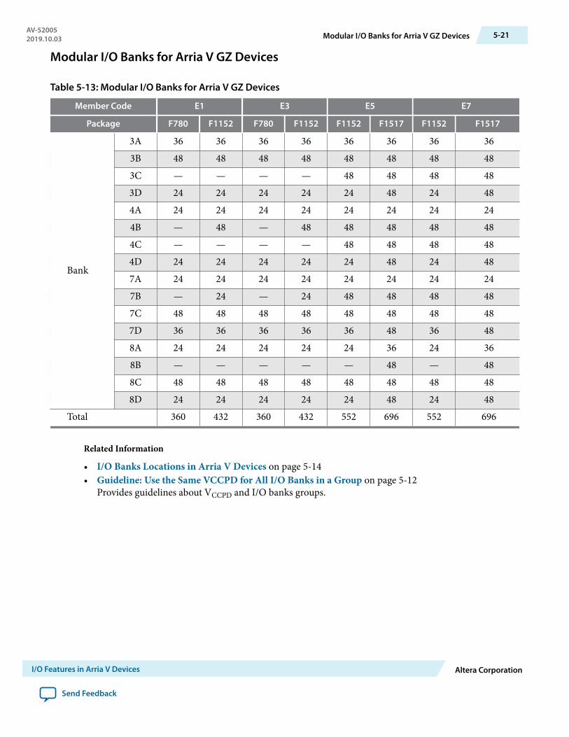
Modular I/O Banks for Arria V GZ Devices
Table 5-13: Modular I/O Banks for Arria V GZ Devices
Member Code E1 E3 E5 E7
Package F780 F1152 F780 F1152 F1152 F1517 F1152 F1517
Bank
3A 36 36 36 36 36 36 36 363B 48 48 48 48 48 48 48 483C — — — — 48 48 48 483D 24 24 24 24 24 48 24 484A 24 24 24 24 24 24 24 244B — 48 — 48 48 48 48 484C — — — — 48 48 48 484D 24 24 24 24 24 48 24 487A 24 24 24 24 24 24 24 247B — 24 — 24 48 48 48 487C 48 48 48 48 48 48 48 487D 36 36 36 36 36 48 36 488A 24 24 24 24 24 36 24 368B — — — — — 48 — 488C 48 48 48 48 48 48 48 488D 24 24 24 24 24 48 24 48
Total 360 432 360 432 552 696 552 696
Related Information
• I/O Banks Locations in Arria V Devices on page 5-14• Guideline: Use the Same VCCPD for All I/O Banks in a Group on page 5-12
Provides guidelines about VCCPD and I/O banks groups.
AV-520052019.10.03 Modular I/O Banks for Arria V GZ Devices 5-21
I/O Features in Arria V Devices Altera Corporation
Send Feedback
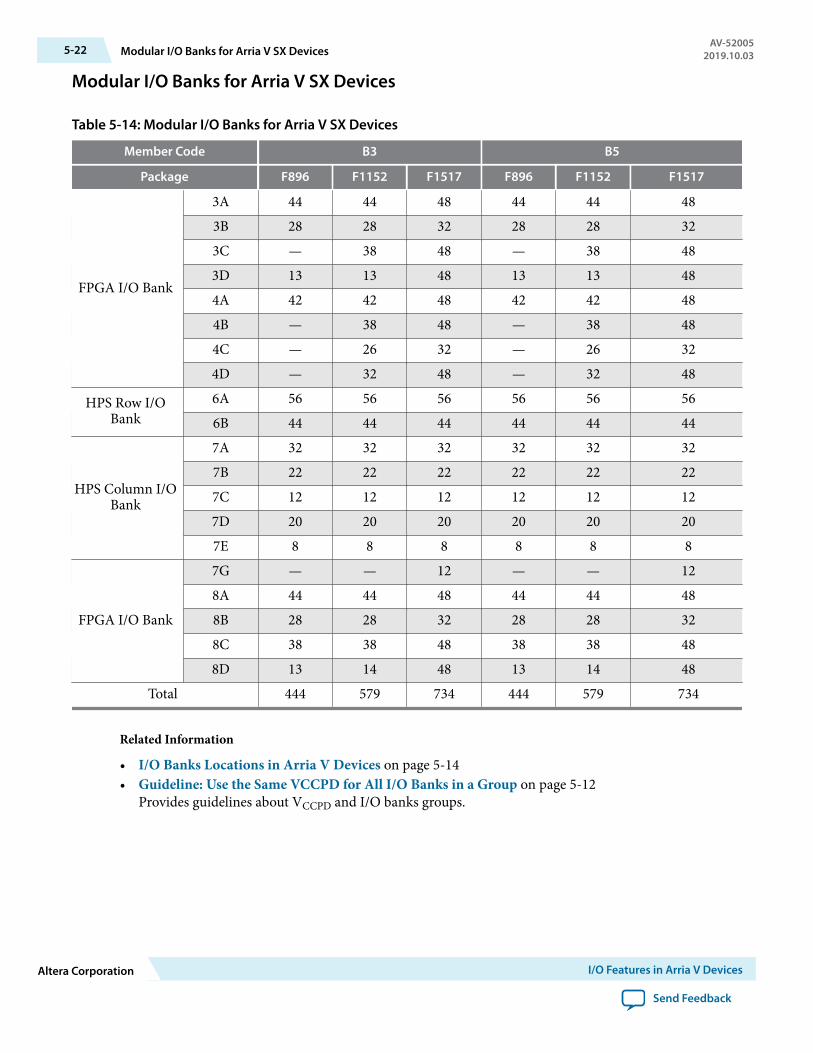
Modular I/O Banks for Arria V SX Devices
Table 5-14: Modular I/O Banks for Arria V SX Devices
Member Code B3 B5
Package F896 F1152 F1517 F896 F1152 F1517
FPGA I/O Bank
3A 44 44 48 44 44 483B 28 28 32 28 28 323C — 38 48 — 38 483D 13 13 48 13 13 484A 42 42 48 42 42 484B — 38 48 — 38 484C — 26 32 — 26 324D — 32 48 — 32 48
HPS Row I/OBank
6A 56 56 56 56 56 566B 44 44 44 44 44 44
HPS Column I/OBank
7A 32 32 32 32 32 327B 22 22 22 22 22 227C 12 12 12 12 12 127D 20 20 20 20 20 207E 8 8 8 8 8 8
FPGA I/O Bank
7G — — 12 — — 128A 44 44 48 44 44 488B 28 28 32 28 28 328C 38 38 48 38 38 488D 13 14 48 13 14 48
Total 444 579 734 444 579 734
Related Information
• I/O Banks Locations in Arria V Devices on page 5-14• Guideline: Use the Same VCCPD for All I/O Banks in a Group on page 5-12
Provides guidelines about VCCPD and I/O banks groups.
5-22 Modular I/O Banks for Arria V SX DevicesAV-52005
2019.10.03
Altera Corporation I/O Features in Arria V Devices
Send Feedback

Modular I/O Banks for Arria V ST Devices
Table 5-15: Modular I/O Banks for Arria V ST Devices
Member Code D3 D5
Package F896 F1152 F1517 F896 F1152 F1517
FPGA I/O Bank
3A 44 44 48 44 44 483B 28 28 32 28 28 323C — 38 48 — 38 483D 13 13 48 13 13 484A 42 42 48 42 42 484B — 38 48 — 38 484C — 26 32 — 26 324D — 32 48 — 32 48
HPS Row I/OBank
6A 56 56 56 56 56 566B 44 44 44 44 44 44
HPS Column I/OBank
7A 32 32 32 32 32 327B 22 22 22 22 22 227C 12 12 12 12 12 127D 20 20 20 20 20 207E 8 8 8 8 8 8
FPGA I/O Bank
7G — — 12 — — 128A 44 44 48 44 44 488B 28 28 32 28 28 328C 38 38 48 38 38 488D 13 14 48 13 14 48
Total 444 579 734 444 579 734
Related Information
• I/O Banks Locations in Arria V Devices on page 5-14• Guideline: Use the Same VCCPD for All I/O Banks in a Group on page 5-12
Provides guidelines about VCCPD and I/O banks groups.
I/O Element Structure in Arria V DevicesThe I/O elements (IOEs) in Arria V devices contain a bidirectional I/O buffer and I/O registers to supporta complete embedded bidirectional single data rate (SDR) or double data rate (DDR) transfer.
AV-520052019.10.03 Modular I/O Banks for Arria V ST Devices 5-23
I/O Features in Arria V Devices Altera Corporation
Send Feedback

The IOEs are located in I/O blocks around the periphery of the Arria V device.
The Arria V SX and ST devices also have I/O elements for the HPS.
I/O Buffer and Registers in Arria V DevicesI/O registers are composed of the input path for handling data from the pin to the core, the output path forhandling data from the core to the pin, and the output enable (OE) path for handling the OE signal to theoutput buffer. These registers allow faster source-synchronous register-to-register transfers and resynchro‐nization.
Table 5-16: Input and Output Paths in Arria V Devices
This table summarizes the input and output path in the Arria V devices.Input Path Output Path
Consists of:
• DDR input registers• Alignment and synchronization registers• Half data rate blocks
Consists of:
• Output or OE registers• Alignment registers• Half data rate blocks
You can bypass each block in the input path. Theinput path uses the deskew delay to adjust the inputregister clock delay across process, voltage, andtemperature (PVT) variations.
You can bypass each block of the output and OEpaths.
5-24 I/O Buffer and Registers in Arria V DevicesAV-52005
2019.10.03
Altera Corporation I/O Features in Arria V Devices
Send Feedback

Figure 5-5: IOE Structure for Arria V DevicesThis figure shows the Arria V FPGA IOE structure. In the figure, one dynamic on-chip termination (OCT)control is available for each DQ/DQS group.
4
Open Drain
V CCIOV CCIO
4
PRND Q
PRND Q
PRND Q
PRND Q
PRND Q
OE Register
OE Register
Output Register
Output Register
clkout
D5 Delay
Input Register
PRND Q
Input RegisterPRN
D Q
Input Register
clkin
D5 Delay
OutputBuffer
Input Buffer
D5_OCT
From Core
DQS Logic Block
Dynamic OCT Control
D4 DelayDQSCQn
2 OEfromCore
Same available settings in the Quartus II software
OptionalPCI ClampWrite
DatafromCore
Half DataRate Block
Half DataRate Block
On-ChipTermination
ProgrammablePull-Up Resistor
ProgrammableCurrent
Strength and Slew Rate
Control
D1Delay
D3_0Delay
ReadFIFO
D3_1Delay
ToCoreToCore
ReadDatatoCore
From OCTCalibration
Block
Bus-HoldCircuit
AV-520052019.10.03 I/O Buffer and Registers in Arria V Devices 5-25
I/O Features in Arria V Devices Altera Corporation
Send Feedback

Programmable IOE Features in Arria V Devices
Table 5-17: Summary of Supported Arria V Programmable IOE Features and Settings
Feature Setting Assignment Name Supported I/O Standards Supported in HPSI/O
(SoC Devices Only)
Slew RateControl(16)
• 0 (Slow)• 1 (Fast). Default
is 1.
Slew Rate • 3.0/3.3V LVTTL• 1.2/1.5/1.8/2.5/3.0/3.3
LVCMOS• SSTL-2/SSTL-18/SSTL-15• 1.8/1.5/1.2V HSTL• 3.0V PCI• 3.0V PCI-X• Differential SSTL-2/
Differential SSTL-18/Differential SSTL-15
• Differential 1.2/1.5/1.8VHSTL
Yes
Program‐mableOutputBuffer Delay
• 0 ps (Default)• 50 ps• 100 ps• 150 ps
Output BufferDelay
• 3.0/3.3-V LVTTL• 1.2/1.5/1.8/2.5/3.0/3.3
LVCMOS• SSTL-2, SSTL-18, SSTL-15,
SSTL-135, SSTL-125• 1.8/1.5/1.2 V HSTL• HSUL-12• 3.0V PCI• 3.0V PCI-X• Differential SSTL-2/Diff-
SSTL-18/Differential SSTL-15/Differential SSTL-135/Differential SSTL-125
• Differential 1.2/1.5/1.8VHSTL
• Differential 1.2-V HSUL
—
(16) Disabled if you use the RS OCT feature.
5-26 Programmable IOE Features in Arria V DevicesAV-52005
2019.10.03
Altera Corporation I/O Features in Arria V Devices
Send Feedback
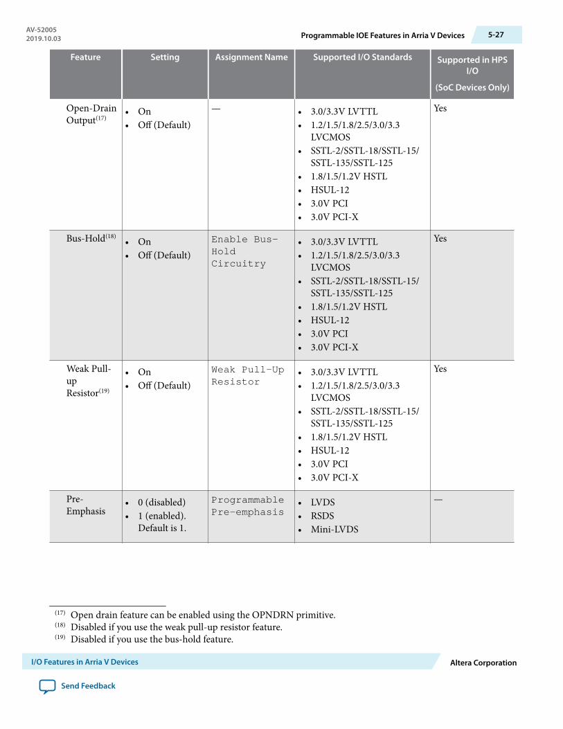
Feature Setting Assignment Name Supported I/O Standards Supported in HPSI/O
(SoC Devices Only)
Open-DrainOutput(17)
• On• Off (Default)
— • 3.0/3.3V LVTTL• 1.2/1.5/1.8/2.5/3.0/3.3
LVCMOS• SSTL-2/SSTL-18/SSTL-15/
SSTL-135/SSTL-125• 1.8/1.5/1.2V HSTL• HSUL-12• 3.0V PCI• 3.0V PCI-X
Yes
Bus-Hold(18) • On• Off (Default)
Enable Bus-HoldCircuitry
• 3.0/3.3V LVTTL• 1.2/1.5/1.8/2.5/3.0/3.3
LVCMOS• SSTL-2/SSTL-18/SSTL-15/
SSTL-135/SSTL-125• 1.8/1.5/1.2V HSTL• HSUL-12• 3.0V PCI• 3.0V PCI-X
Yes
Weak Pull-upResistor(19)
• On• Off (Default)
Weak Pull-UpResistor
• 3.0/3.3V LVTTL• 1.2/1.5/1.8/2.5/3.0/3.3
LVCMOS• SSTL-2/SSTL-18/SSTL-15/
SSTL-135/SSTL-125• 1.8/1.5/1.2V HSTL• HSUL-12• 3.0V PCI• 3.0V PCI-X
Yes
Pre-Emphasis
• 0 (disabled)• 1 (enabled).
Default is 1.
ProgrammablePre-emphasis
• LVDS• RSDS• Mini-LVDS
—
(17) Open drain feature can be enabled using the OPNDRN primitive.(18) Disabled if you use the weak pull-up resistor feature.(19) Disabled if you use the bus-hold feature.
AV-520052019.10.03 Programmable IOE Features in Arria V Devices 5-27
I/O Features in Arria V Devices Altera Corporation
Send Feedback
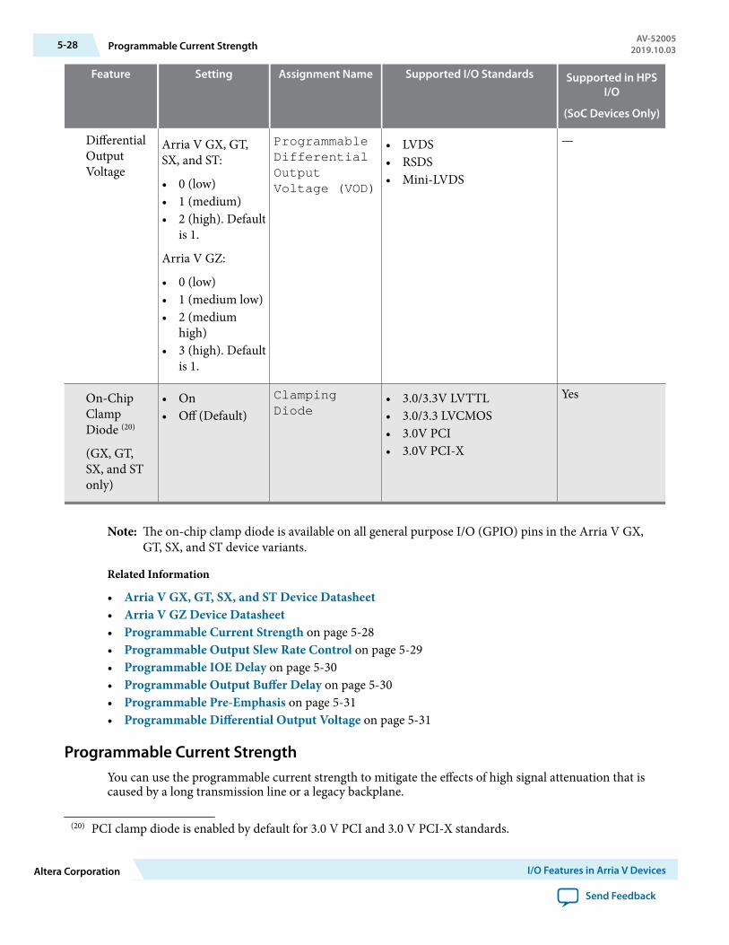
Feature Setting Assignment Name Supported I/O Standards Supported in HPSI/O
(SoC Devices Only)
DifferentialOutputVoltage
Arria V GX, GT,SX, and ST:
• 0 (low)• 1 (medium)• 2 (high). Default
is 1.
Arria V GZ:
• 0 (low)• 1 (medium low)• 2 (medium
high)• 3 (high). Default
is 1.
ProgrammableDifferentialOutputVoltage (VOD)
• LVDS• RSDS• Mini-LVDS
—
On-ChipClampDiode (20)
(GX, GT,SX, and STonly)
• On• Off (Default)
ClampingDiode
• 3.0/3.3V LVTTL• 3.0/3.3 LVCMOS• 3.0V PCI• 3.0V PCI-X
Yes
Note: The on-chip clamp diode is available on all general purpose I/O (GPIO) pins in the Arria V GX,GT, SX, and ST device variants.
Related Information
• Arria V GX, GT, SX, and ST Device Datasheet• Arria V GZ Device Datasheet• Programmable Current Strength on page 5-28• Programmable Output Slew Rate Control on page 5-29• Programmable IOE Delay on page 5-30• Programmable Output Buffer Delay on page 5-30• Programmable Pre-Emphasis on page 5-31• Programmable Differential Output Voltage on page 5-31
Programmable Current StrengthYou can use the programmable current strength to mitigate the effects of high signal attenuation that iscaused by a long transmission line or a legacy backplane.
(20) PCI clamp diode is enabled by default for 3.0 V PCI and 3.0 V PCI-X standards.
5-28 Programmable Current StrengthAV-52005
2019.10.03
Altera Corporation I/O Features in Arria V Devices
Send Feedback

Table 5-18: Programmable Current Strength Settings for Arria V Devices
The output buffer for each Arria V device I/O pin has a programmable current strength control for the I/Ostandards listed in this table.
I/O Standard
I OH / I OL Current Strength Setting (mA)
(Default setting in bold)Supported in HPS
(SoC Devices Only)Arria V GX, GT, SX, and ST Arria V GZ
3.3-V LVTTL 8 , 4 16, 12 , 8, 4 Yes3.3-V LVCMOS 2 16, 12 , 8, 4 Yes3.0-V LVTTL 16, 12 , 8, 4 — Yes3.0-V LVCMOS 16, 12 , 8, 4 — Yes2.5-V LVCMOS 16, 12 , 8, 4 16, 12 , 8, 4 Yes1.8-V LVCMOS 12 , 10, 8, 6, 4, 2 12 , 10, 8, 6, 4, 2 Yes1.5-V LVCMOS 12 , 10, 8, 6, 4, 2 12 , 10, 8, 6, 4, 2 Yes1.2-V LVCMOS 8 , 6, 4, 2 8 , 6, 4, 2 —SSTL-2 Class I 12, 10, 8 12, 10, 8 —SSTL-2 Class II 16 16 —SSTL-18 Class I 12, 10, 8 , 6, 4 12, 10, 8 , 6, 4 YesSSTL-18 Class II 16 16 , 8 YesSSTL-15 Class I 12, 10, 8 , 6, 4 12, 10, 8 , 6, 4 YesSSTL-15 Class II 16 16 , 8 Yes1.8-V HSTL Class I 12, 10, 8 , 6, 4 12, 10, 8 , 6, 4 —1.8-V HSTL Class II 16 16 —1.5-V HSTL Class I 12, 10, 8 , 6, 4 12, 10, 8 , 6, 4 Yes1.5-V HSTL Class II 16 16 Yes1.2-V HSTL Class I 12, 10, 8 , 6, 4 12, 10, 8 , 6, 4 —1.2-V HSTL Class II 16 16 —
For the Arria V GZ devices, the 3.3 V LVTTL and 3.3 V LVCMOS I/O standards are supported using VCCIO and V CCPD at 3.0 V .
Note: Intel recommends that you perform IBIS or SPICE simulations to determine the best currentstrength setting for your specific application.
Related InformationProgrammable IOE Features in Arria V Devices on page 5-26
Programmable Output Slew Rate ControlProgrammable output slew rate is available for single-ended I/O standards and emulated LVDS outputstandards.
AV-520052019.10.03 Programmable Output Slew Rate Control 5-29
I/O Features in Arria V Devices Altera Corporation
Send Feedback
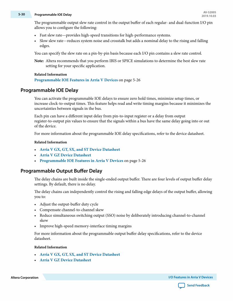
The programmable output slew rate control in the output buffer of each regular- and dual-function I/O pinallows you to configure the following:
• Fast slew rate—provides high-speed transitions for high-performance systems.• Slow slew rate—reduces system noise and crosstalk but adds a nominal delay to the rising and falling
edges.
You can specify the slew rate on a pin-by-pin basis because each I/O pin contains a slew rate control.
Note: Altera recommends that you perform IBIS or SPICE simulations to determine the best slew ratesetting for your specific application.
Related InformationProgrammable IOE Features in Arria V Devices on page 5-26
Programmable IOE DelayYou can activate the programmable IOE delays to ensure zero hold times, minimize setup times, orincrease clock-to-output times. This feature helps read and write timing margins because it minimizes theuncertainties between signals in the bus.
Each pin can have a different input delay from pin-to-input register or a delay from outputregister-to-output pin values to ensure that the signals within a bus have the same delay going into or outof the device.
For more information about the programmable IOE delay specifications, refer to the device datasheet.
Related Information
• Arria V GX, GT, SX, and ST Device Datasheet• Arria V GZ Device Datasheet• Programmable IOE Features in Arria V Devices on page 5-26
Programmable Output Buffer DelayThe delay chains are built inside the single-ended output buffer. There are four levels of output buffer delaysettings. By default, there is no delay.
The delay chains can independently control the rising and falling edge delays of the output buffer, allowingyou to:
• Adjust the output-buffer duty cycle• Compensate channel-to-channel skew• Reduce simultaneous switching output (SSO) noise by deliberately introducing channel-to-channel
skew• Improve high-speed memory-interface timing margins
For more information about the programmable output buffer delay specifications, refer to the devicedatasheet.
Related Information
• Arria V GX, GT, SX, and ST Device Datasheet• Arria V GZ Device Datasheet
5-30 Programmable IOE DelayAV-52005
2019.10.03
Altera Corporation I/O Features in Arria V Devices
Send Feedback
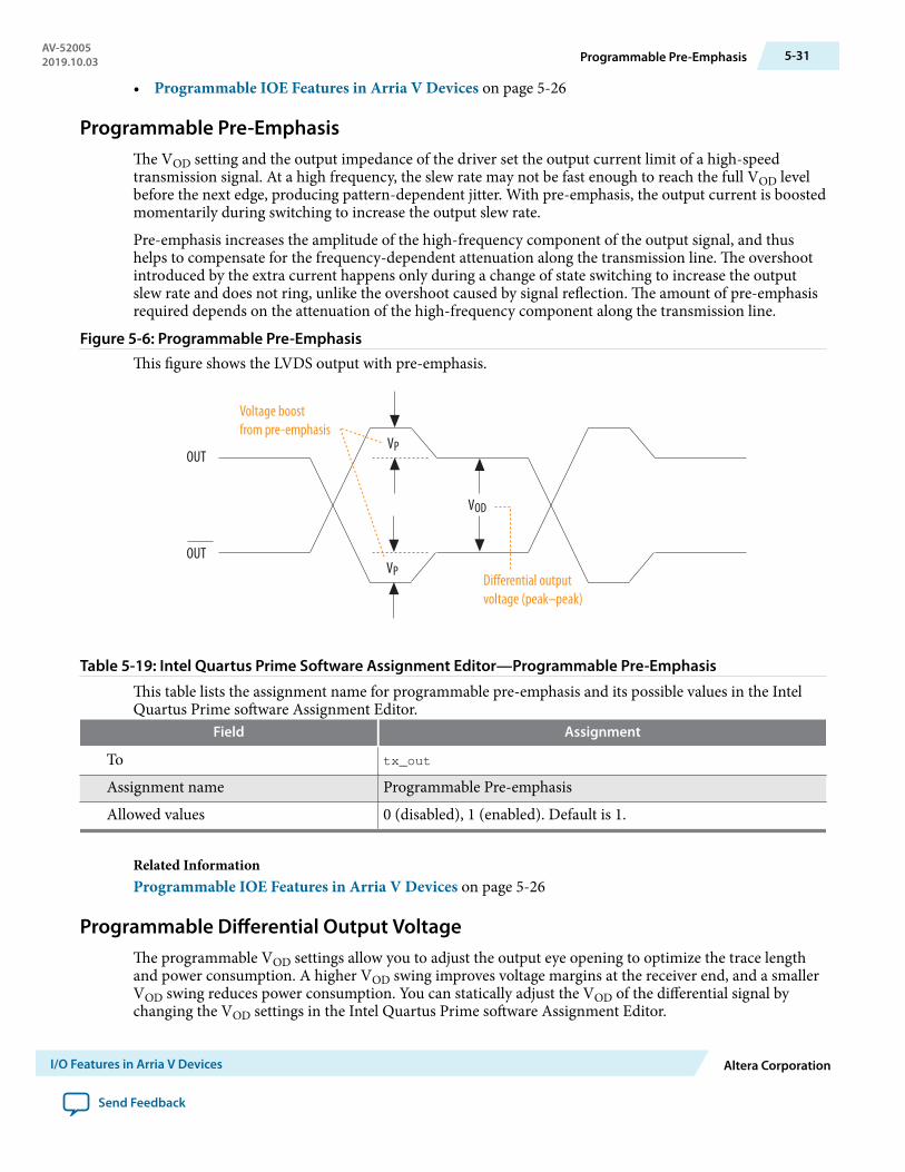
• Programmable IOE Features in Arria V Devices on page 5-26
Programmable Pre-EmphasisThe VOD setting and the output impedance of the driver set the output current limit of a high-speedtransmission signal. At a high frequency, the slew rate may not be fast enough to reach the full VOD levelbefore the next edge, producing pattern-dependent jitter. With pre-emphasis, the output current is boostedmomentarily during switching to increase the output slew rate.
Pre-emphasis increases the amplitude of the high-frequency component of the output signal, and thushelps to compensate for the frequency-dependent attenuation along the transmission line. The overshootintroduced by the extra current happens only during a change of state switching to increase the outputslew rate and does not ring, unlike the overshoot caused by signal reflection. The amount of pre-emphasisrequired depends on the attenuation of the high-frequency component along the transmission line.
Figure 5-6: Programmable Pre-EmphasisThis figure shows the LVDS output with pre-emphasis.
OUT
OUT
VOD
VP
VP
Voltage boostfrom pre-emphasis
Differential outputvoltage (peak–peak)
Table 5-19: Intel Quartus Prime Software Assignment Editor—Programmable Pre-Emphasis
This table lists the assignment name for programmable pre-emphasis and its possible values in the IntelQuartus Prime software Assignment Editor.
Field Assignment
To tx_out
Assignment name Programmable Pre-emphasisAllowed values 0 (disabled), 1 (enabled). Default is 1.
Related InformationProgrammable IOE Features in Arria V Devices on page 5-26
Programmable Differential Output VoltageThe programmable VOD settings allow you to adjust the output eye opening to optimize the trace lengthand power consumption. A higher VOD swing improves voltage margins at the receiver end, and a smallerVOD swing reduces power consumption. You can statically adjust the VOD of the differential signal bychanging the VOD settings in the Intel Quartus Prime software Assignment Editor.
AV-520052019.10.03 Programmable Pre-Emphasis 5-31
I/O Features in Arria V Devices Altera Corporation
Send Feedback

Figure 5-7: Differential VOD
This figure shows the VOD of the differential LVDS output.
Single-Ended Waveform
Positive Channel (p)
Negative Channel (n)
Ground
Differential Waveform
p - n = 0 V
VCM
VOD
VOD
VOD
VOD (diff peak - peak) = 2 x VOD (single-ended)
Table 5-20: Intel Quartus Prime Software Assignment Editor—Programmable VOD
This table lists the assignment name for programmable VOD and its possible values in the Intel QuartusPrime software Assignment Editor.
Field Assignment
To tx_out
Assignment name Programmable Differential Output Voltage (VOD)Allowed values • Arria V GX, GT, SX, and ST—0 (low), 1 (medium), 2 (high).
Default is 1.• Arria V GZ—0 (low), 1 (medium low), 2 (medium high), 3
(high). Default is 1.
Related InformationProgrammable IOE Features in Arria V Devices on page 5-26
Open-Drain OutputThe optional open-drain output for each I/O pin is equivalent to an open collector output. If it isconfigured as an open drain, the logic value of the output is either high-Z or logic low.
You can attach several open-drain output to a wire. This connection type is like a logical OR function andis commonly called an active-low wired-OR circuit. If at least one of the outputs is in logic 0 state (active),the circuit sinks the current and brings the line to low voltage.
You can use open-drain output if you are connecting multiple devices to a bus. For example, you can usethe open-drain output for system-level control signals that can be asserted by any device or as an interrupt.
You can enable the open-drain output assignment using one these methods:
5-32 Open-Drain OutputAV-52005
2019.10.03
Altera Corporation I/O Features in Arria V Devices
Send Feedback

• Design the tristate buffer using OPNDRN primitive.• Turn on the Auto Open-Drain Pins option in the Intel Quartus Prime software.
Although you can design open-drain output without enabling the option assignment, you will not be usingthe open-drain output feature of the I/O buffer. The open-drain output feature in the I/O buffer providesyou the best propagation delay from OE to output.
Pull-up ResistorEach I/O pin provides an optional programmable pull-up resistor during user mode. The pull-up resistor,typically 25 kΩ, weakly holds the I/O to the VCCIO level. If you enable this option, you cannot use the bus-hold feature.
The Arria V device supports programmable weak pull-up resistors only on user I/O pins.
For dedicated configuration pins, dedicated clock pins, or JTAG pins with internal pull-up resistors, theseresistor values are not programmable. You can find more information related to the internal pull-up valuesfor dedicated configuration pins, dedicated clock pins, or JTAG pins in the Arria V Pin ConnectionGuidelines.
Bus-Hold CircuitryEach I/O pin provides an optional bus-hold feature that is active only after configuration. When the deviceenters user mode, the bus-hold circuit captures the value that is present on the pin by the end of theconfiguration.
The bus-hold circuitry uses a resistor with a nominal resistance (RBH), approximately 7 kΩ, to weakly pullthe signal level to the last-driven state of the pin. The bus-hold circuitry holds this pin state until the nextinput signal is present. Because of this, you do not require an external pull-up or pull-down resistor tohold a signal level when the bus is tri-stated.
For each I/O pin, you can individually specify that the bus-hold circuitry pulls non-driven pins away fromthe input threshold voltage—where noise can cause unintended high-frequency switching. To preventover-driving signals, the bus-hold circuitry drives the voltage level of the I/O pin lower than the VCCIOlevel.
If you enable the bus-hold feature, you cannot use the programmable pull-up option. To configure the I/Opin for differential signals, disable the bus-hold feature.
On-Chip I/O Termination in Arria V DevicesDynamic RS and RT OCT provides I/O impedance matching and termination capabilities. OCT maintainssignal quality, saves board space, and reduces external component costs.
The Arria V devices support OCT in all FPGA I/O banks. For the HPS I/Os, the column I/Os do notsupport OCT with calibration.
AV-520052019.10.03 Pull-up Resistor 5-33
I/O Features in Arria V Devices Altera Corporation
Send Feedback

Table 5-21: OCT Schemes Supported in Arria V Devices
Direction OCT Schemes Supported in HPS Row I/Os
OutputRS OCT with calibration Yes
RS OCT withoutcalibration
Yes
InputRT OCT with calibration Yes
RD OCT (LVDS I/Ostandard only)
—
Bidirectional Dynamic RS OCT and RTOCT
Yes
RS OCT without Calibration in Arria V DevicesThe Arria V devices support RS OCT for single-ended and voltage-referenced I/O standards. RS OCTwithout calibration is supported on output only.
Table 5-22: Selectable I/O Standards for RS OCT Without Calibration
This table lists the output termination settings for uncalibrated OCT on different I/O standards.
I/O Standard Device Variant SupportUncalibrated OCT (Output)
RS (Ω)
3.3 V LVTTL/3.3 V LVCMOS GZ only 25/503.0 V LVTTL/3.0 V LVCMOS GX, GT, SX, and ST 25/502.5 V LVCMOS All 25/501.8 V LVCMOS All 25/501.5 V LVCMOS All 25/501.2 V LVCMOS All 25/50SSTL-2 Class I All 50SSTL-2 Class II All 25SSTL-18 Class I All 50SSTL-18 Class II All 25SSTL-15 Class I All 50SSTL-15 Class II All 251.8 V HSTL Class I All 501.8 V HSTL Class II All 251.5 V HSTL Class I All 501.5 V HSTL Class II All 251.2 V HSTL Class I All 50
5-34 RS OCT without Calibration in Arria V DevicesAV-52005
2019.10.03
Altera Corporation I/O Features in Arria V Devices
Send Feedback
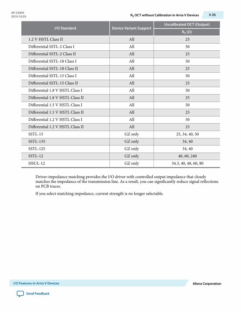
I/O Standard Device Variant SupportUncalibrated OCT (Output)
RS (Ω)
1.2 V HSTL Class II All 25Differential SSTL-2 Class I All 50Differential SSTL-2 Class II All 25Differential SSTL-18 Class I All 50Differential SSTL-18 Class II All 25Differential SSTL-15 Class I All 50Differential SSTL-15 Class II All 25Differential 1.8 V HSTL Class I All 50Differential 1.8 V HSTL Class II All 25Differential 1.5 V HSTL Class I All 50Differential 1.5 V HSTL Class II All 25Differential 1.2 V HSTL Class I All 50Differential 1.2 V HSTL Class II All 25SSTL-15 GZ only 25, 34, 40, 50SSTL-135 GZ only 34, 40SSTL-125 GZ only 34, 40SSTL-12 GZ only 40, 60, 240HSUL-12 GZ only 34.3, 40, 48, 60, 80
Driver-impedance matching provides the I/O driver with controlled output impedance that closelymatches the impedance of the transmission line. As a result, you can significantly reduce signal reflectionson PCB traces.
If you select matching impedance, current strength is no longer selectable.
AV-520052019.10.03 RS OCT without Calibration in Arria V Devices 5-35
I/O Features in Arria V Devices Altera Corporation
Send Feedback

Figure 5-8: RS OCT Without CalibrationThis figure shows the RS as the intrinsic impedance of the output transistors.
V CCIO
R S
R S
GND
Z 0 = 50 Ω
DriverSeries Termination
ReceivingDevice
RS OCT with Calibration in Arria V DevicesThe Arria V devices support RS OCT with calibration in all banks.
Table 5-23: Selectable I/O Standards for RS OCT With Calibration
This table lists the output termination settings for calibrated OCT on different I/O standards.
I/O Standard Device VariantSupport
Calibrated OCT (Output)
RS (Ω) RZQ (Ω)
3.3 V LVTTL/3.3 V LVCMOS GZ only 25/50 1003.0 V LVTTL/3.0 V LVCMOS GX, GT, SX, and
ST25/50 100
2.5 V LVCMOS All 25/50 1001.8 V LVCMOS All 25/50 1001.5 V LVCMOS All 25/50 1001.2 V LVCMOS All 25/50 100SSTL-2 Class I All 50 100SSTL-2 Class II All 25 100SSTL-18 Class I All 50 100SSTL-18 Class II All 25 100SSTL-15 Class I All 50 100SSTL-15 Class II All 25 1001.8 V HSTL Class I All 50 1001.8 V HSTL Class II All 25 1001.5 V HSTL Class I All 50 100
5-36 RS OCT with Calibration in Arria V DevicesAV-52005
2019.10.03
Altera Corporation I/O Features in Arria V Devices
Send Feedback

I/O Standard Device VariantSupport
Calibrated OCT (Output)
RS (Ω) RZQ (Ω)
1.5 V HSTL Class II All 25 1001.2 V HSTL Class I All 50 1001.2 V HSTL Class II All 25 100Differential SSTL-2 Class I All 50 100Differential SSTL-2 Class II All 25 100Differential SSTL-18 Class I All 50 100Differential SSTL-18 Class II All 25 100Differential SSTL-15 Class I All 50 100Differential SSTL-15 Class II All 25 100Differential 1.8 V HSTL Class I All 50 100Differential 1.8 V HSTL Class II All 25 100Differential 1.5 V HSTL Class I All 50 100Differential 1.5 V HSTL Class II All 25 100Differential 1.2 V HSTL Class I All 50 100Differential 1.2 V HSTL Class II All 25 100
SSTL-15All 25, 50 100All 34, 40 240
SSTL-135 All 34, 40 240SSTL-125 All 34, 40 240SSTL-12 GZ only 40, 60, 240 240HSUL-12 All 34, 40, 48, 60, 80 240
Differential SSTL-15All 25, 50 100All 34, 40 240
Differential SSTL-135 All 34, 40 240Differential SSTL-125 All 34, 40 240Differential SSTL-12 GZ only 40, 60, 240 240Differential HSUL-12 All 34, 40, 48, 60, 80 240
The RS OCT calibration circuit compares the total impedance of the I/O buffer to the external referenceresistor connected to the RZQ pin and dynamically enables or disables the transistors until they match.
Calibration occurs at the end of device configuration. When the calibration circuit finds the correctimpedance, the circuit powers down and stops changing the characteristics of the drivers.
AV-520052019.10.03 RS OCT with Calibration in Arria V Devices 5-37
I/O Features in Arria V Devices Altera Corporation
Send Feedback

Figure 5-9: RS OCT with CalibrationThis figure shows the RS as the intrinsic impedance of the output transistors.
V CCIO
R S
R S
GND
Z 0 = 50 Ω
DriverSeries Termination
ReceivingDevice
RT OCT with Calibration in Arria V DevicesThe Arria V devices support RT OCT with calibration in all banks. RT OCT with calibration is availableonly for configuration of input and bidirectional pins. Output pin configurations do not support RT OCTwith calibration. If you use RT OCT, the VCCIO of the bank must match the I/O standard of the pin whereyou enable the RT OCT.
Table 5-24: Selectable I/O Standards for RT OCT With Calibration
This table lists the input termination settings for calibrated OCT on different I/O standards.
I/O Standard Device VariantSupport
Calibrated OCT (Input)
RT (Ω) RZQ (Ω)
SSTL-2 Class I All 50 100SSTL-2 Class II All 50 100SSTL-18 Class I All 50 100SSTL-18 Class II All 50 100SSTL-15 Class I All 50 100SSTL-15 Class II All 50 1001.8 V HSTL Class I All 50 1001.8 V HSTL Class II All 50 1001.5 V HSTL Class I All 50 1001.5 V HSTL Class II All 50 1001.2 V HSTL Class I All 50 1001.2 V HSTL Class II All 50 100Differential SSTL-2 Class I All 50 100
5-38 RT OCT with Calibration in Arria V DevicesAV-52005
2019.10.03
Altera Corporation I/O Features in Arria V Devices
Send Feedback
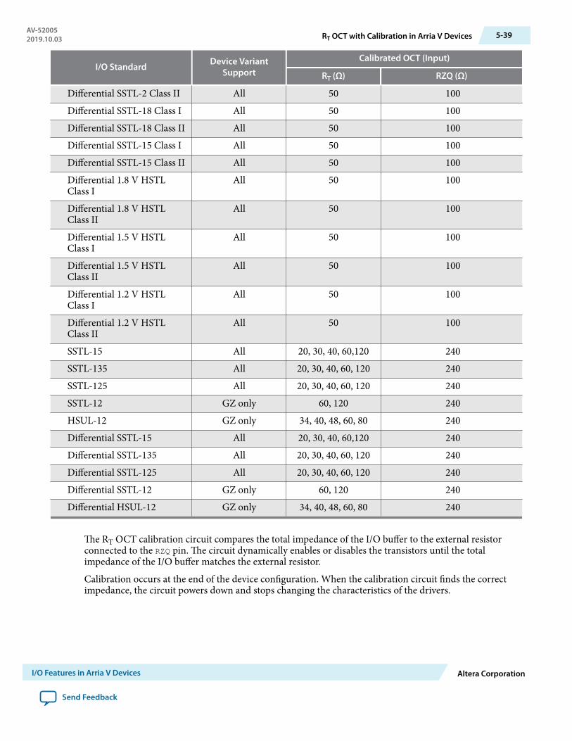
I/O Standard Device VariantSupport
Calibrated OCT (Input)
RT (Ω) RZQ (Ω)
Differential SSTL-2 Class II All 50 100Differential SSTL-18 Class I All 50 100Differential SSTL-18 Class II All 50 100Differential SSTL-15 Class I All 50 100Differential SSTL-15 Class II All 50 100Differential 1.8 V HSTLClass I
All 50 100
Differential 1.8 V HSTLClass II
All 50 100
Differential 1.5 V HSTLClass I
All 50 100
Differential 1.5 V HSTLClass II
All 50 100
Differential 1.2 V HSTLClass I
All 50 100
Differential 1.2 V HSTLClass II
All 50 100
SSTL-15 All 20, 30, 40, 60,120 240SSTL-135 All 20, 30, 40, 60, 120 240SSTL-125 All 20, 30, 40, 60, 120 240SSTL-12 GZ only 60, 120 240HSUL-12 GZ only 34, 40, 48, 60, 80 240Differential SSTL-15 All 20, 30, 40, 60,120 240Differential SSTL-135 All 20, 30, 40, 60, 120 240Differential SSTL-125 All 20, 30, 40, 60, 120 240Differential SSTL-12 GZ only 60, 120 240Differential HSUL-12 GZ only 34, 40, 48, 60, 80 240
The RT OCT calibration circuit compares the total impedance of the I/O buffer to the external resistorconnected to the RZQ pin. The circuit dynamically enables or disables the transistors until the totalimpedance of the I/O buffer matches the external resistor.
Calibration occurs at the end of the device configuration. When the calibration circuit finds the correctimpedance, the circuit powers down and stops changing the characteristics of the drivers.
AV-520052019.10.03 RT OCT with Calibration in Arria V Devices 5-39
I/O Features in Arria V Devices Altera Corporation
Send Feedback
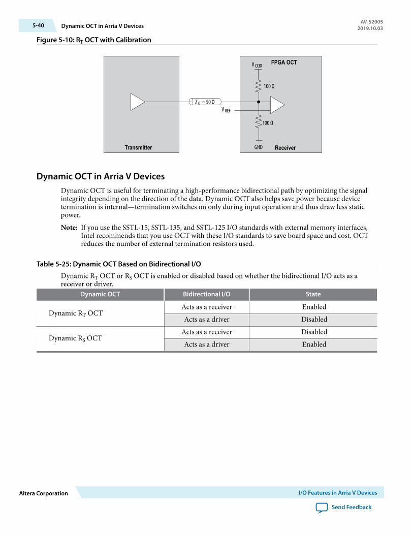
Figure 5-10: RT OCT with Calibration
Transmitter Receiver
FPGA OCT
GND
100 Ω
100 Ω
Z 0 = 50 ΩV REF
V CCIO
Dynamic OCT in Arria V DevicesDynamic OCT is useful for terminating a high-performance bidirectional path by optimizing the signalintegrity depending on the direction of the data. Dynamic OCT also helps save power because devicetermination is internal—termination switches on only during input operation and thus draw less staticpower.
Note: If you use the SSTL-15, SSTL-135, and SSTL-125 I/O standards with external memory interfaces,Intel recommends that you use OCT with these I/O standards to save board space and cost. OCTreduces the number of external termination resistors used.
Table 5-25: Dynamic OCT Based on Bidirectional I/O
Dynamic RT OCT or RS OCT is enabled or disabled based on whether the bidirectional I/O acts as areceiver or driver.
Dynamic OCT Bidirectional I/O State
Dynamic RT OCTActs as a receiver EnabledActs as a driver Disabled
Dynamic RS OCTActs as a receiver DisabledActs as a driver Enabled
5-40 Dynamic OCT in Arria V DevicesAV-52005
2019.10.03
Altera Corporation I/O Features in Arria V Devices
Send Feedback
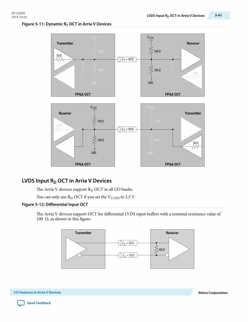
Figure 5-11: Dynamic RT OCT in Arria V Devices
TransmitterReceiver
50 Ω100 Ω
100 Ω50 Ω
GND
Transmitter Receiver
FPGA OCT FPGA OCT
Z 0 = 50 Ω
V CCIO
100 Ω
100 Ω
GND
V CCIO
50 Ω100 Ω
100 Ω50 Ω
GND
FPGA OCT FPGA OCT
Z 0 = 50 Ω
V CCIO
100 Ω
100 Ω
GND
V CCIO
LVDS Input RD OCT in Arria V DevicesThe Arria V devices support RD OCT in all I/O banks.
You can only use RD OCT if you set the VCCPD to 2.5 V.
Figure 5-12: Differential Input OCT
The Arria V devices support OCT for differential LVDS input buffers with a nominal resistance value of100 Ω, as shown in this figure.
100 Ω
ReceiverTransmitter
Z 0 = 50 Ω
Z 0 = 50 Ω
AV-520052019.10.03 LVDS Input RD OCT in Arria V Devices 5-41
I/O Features in Arria V Devices Altera Corporation
Send Feedback
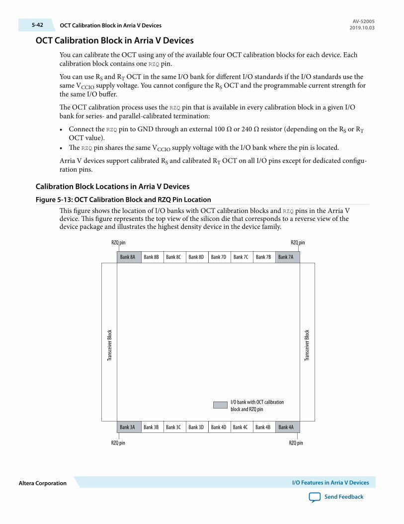
OCT Calibration Block in Arria V DevicesYou can calibrate the OCT using any of the available four OCT calibration blocks for each device. Eachcalibration block contains one RZQ pin.
You can use RS and RT OCT in the same I/O bank for different I/O standards if the I/O standards use thesame VCCIO supply voltage. You cannot configure the RS OCT and the programmable current strength forthe same I/O buffer.
The OCT calibration process uses the RZQ pin that is available in every calibration block in a given I/Obank for series- and parallel-calibrated termination:
• Connect the RZQ pin to GND through an external 100 Ω or 240 Ω resistor (depending on the RS or RTOCT value).
• The RZQ pin shares the same VCCIO supply voltage with the I/O bank where the pin is located.
Arria V devices support calibrated RS and calibrated RT OCT on all I/O pins except for dedicated configu‐ration pins.
Calibration Block Locations in Arria V Devices
Figure 5-13: OCT Calibration Block and RZQ Pin LocationThis figure shows the location of I/O banks with OCT calibration blocks and RZQ pins in the Arria Vdevice. This figure represents the top view of the silicon die that corresponds to a reverse view of thedevice package and illustrates the highest density device in the device family.
I/O bank with OCT calibration block and RZQ pin
Trans
ceive
r Bloc
k
RZQ pin RZQ pin
RZQ pin RZQ pin
Bank 8A Bank 8B Bank 7B Bank 7ABank 7CBank 7DBank 8C Bank 8D
Bank 4ABank 4BBank 3BBank 3A Bank 3C Bank 3D Bank 4CBank 4D
Trans
ceive
r Bloc
k
5-42 OCT Calibration Block in Arria V DevicesAV-52005
2019.10.03
Altera Corporation I/O Features in Arria V Devices
Send Feedback
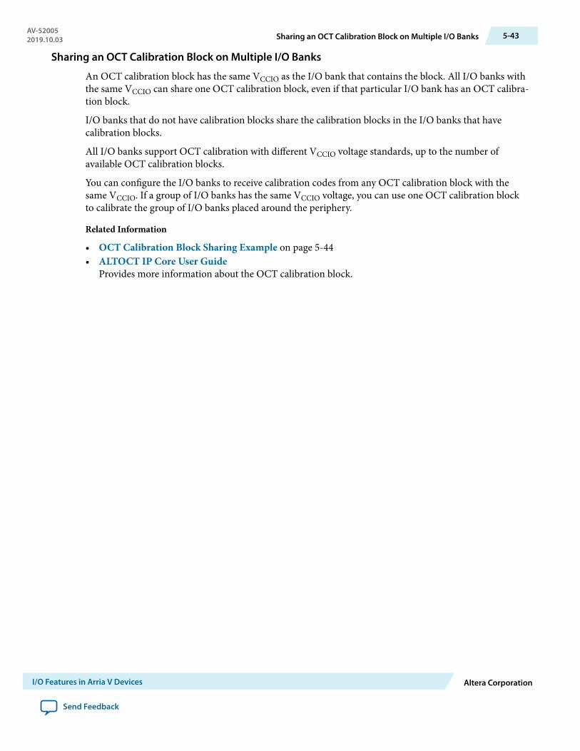
Sharing an OCT Calibration Block on Multiple I/O Banks
An OCT calibration block has the same VCCIO as the I/O bank that contains the block. All I/O banks withthe same VCCIO can share one OCT calibration block, even if that particular I/O bank has an OCT calibra‐tion block.
I/O banks that do not have calibration blocks share the calibration blocks in the I/O banks that havecalibration blocks.
All I/O banks support OCT calibration with different VCCIO voltage standards, up to the number ofavailable OCT calibration blocks.
You can configure the I/O banks to receive calibration codes from any OCT calibration block with thesame VCCIO. If a group of I/O banks has the same VCCIO voltage, you can use one OCT calibration blockto calibrate the group of I/O banks placed around the periphery.
Related Information
• OCT Calibration Block Sharing Example on page 5-44• ALTOCT IP Core User Guide
Provides more information about the OCT calibration block.
AV-520052019.10.03 Sharing an OCT Calibration Block on Multiple I/O Banks 5-43
I/O Features in Arria V Devices Altera Corporation
Send Feedback
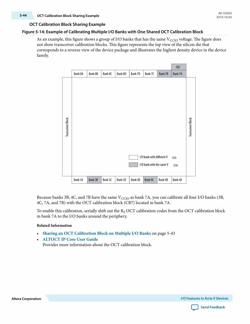
OCT Calibration Block Sharing Example
Figure 5-14: Example of Calibrating Multiple I/O Banks with One Shared OCT Calibration Block
As an example, this figure shows a group of I/O banks that has the same VCCIO voltage. The figure doesnot show transceiver calibration blocks. This figure represents the top view of the silicon die thatcorresponds to a reverse view of the device package and illustrates the highest density device in the devicefamily.
I/O bank with the same V CCIO
I/O bank with different V CCIO
Trans
ceive
r Bloc
kCB7
Bank 8A Bank 8B Bank 7B Bank 7ABank 7CBank 7DBank 8C Bank 8D
Bank 4ABank 4BBank 3BBank 3A Bank 3C Bank 3D Bank 4CBank 4D
Trans
ceive
r Bloc
k
Because banks 3B, 4C, and 7B have the same VCCIO as bank 7A, you can calibrate all four I/O banks (3B,4C, 7A, and 7B) with the OCT calibration block (CB7) located in bank 7A.
To enable this calibration, serially shift out the RS OCT calibration codes from the OCT calibration blockin bank 7A to the I/O banks around the periphery.
Related Information
• Sharing an OCT Calibration Block on Multiple I/O Banks on page 5-43• ALTOCT IP Core User Guide
Provides more information about the OCT calibration block.
5-44 OCT Calibration Block Sharing ExampleAV-52005
2019.10.03
Altera Corporation I/O Features in Arria V Devices
Send Feedback
External I/O Termination for Arria V Devices
Table 5-26: External Termination Schemes for Different I/O Standards
I/O Standard External Termination Scheme
3.3 V LVTTL/3.3 V LVCMOS
No external termination required
3.0 V LVVTL/3.0 V LVCMOS
3.0 V PCI
3.0 V PCI-X
2.5 V LVCMOS
1.8 V LVCMOS
1.5 V LVCMOS
1.2 V LVCMOS
SSTL-2 Class I
Single-Ended SSTL I/O Standard Termination
SSTL-2 Class II
SSTL-18 Class I
SSTL-18 Class II
SSTL-15 Class I
SSTL-15 Class II
1.8 V HSTL Class I
Single-Ended HSTL I/O Standard Termination
1.8 V HSTL Class II
1.5 V HSTL Class I
1.5 V HSTL Class II
1.2 V HSTL Class I
1.2 V HSTL Class II
Differential SSTL-2 Class I
Differential SSTL I/O Standard Termination
Differential SSTL-2 Class II
Differential SSTL-18 Class I
Differential SSTL-18 Class II
Differential SSTL-15 Class I
Differential SSTL-15 Class II
AV-520052019.10.03 External I/O Termination for Arria V Devices 5-45
I/O Features in Arria V Devices Altera Corporation
Send Feedback

I/O Standard External Termination Scheme
Differential 1.8 V HSTL Class I
Differential HSTL I/O Standard Termination
Differential 1.8 V HSTL Class II
Differential 1.5 V HSTL Class I
Differential 1.5 V HSTL Class II
Differential 1.2 V HSTL Class I
Differential 1.2 V HSTL Class II
LVDS LVDS I/O Standard Termination
RSDSRSDS/mini-LVDS I/O Standard Termination
Mini-LVDS
LVPECL Differential LVPECL I/O Standard Termination
SSTL-15 (21)
No external termination required
SSTL-135 (21)
SSTL-125 (21)
SSTL-12
HSUL-12
Differential SSTL-15 (21)
Differential SSTL-135 (21)
Differential SSTL-125 (21)
Differential SSTL-12
Differential HSUL-12
Single-ended I/O TerminationVoltage-referenced I/O standards require an input VREF and a termination voltage (VTT). The referencevoltage of the receiving device tracks the termination voltage of the transmitting device.
The supported I/O standards such as SSTL-12, SSTL-125, SSTL-135, and SSTL-15 typically do not requireexternal board termination.
Intel recommends that you use OCT with these I/O standards to save board space and cost. OCT reducesthe number of external termination resistors used.
Note: You cannot use RS and RT OCT simultaneously. For more information, refer to the related informa‐tion.
(21) Intel recommends that you use OCT with these I/O standards to save board space and cost. OCT reduces thenumber of external termination resistors used.
5-46 Single-ended I/O TerminationAV-52005
2019.10.03
Altera Corporation I/O Features in Arria V Devices
Send Feedback
Figure 5-15: SSTL I/O Standard TerminationThis figure shows the details of SSTL I/O termination on Arria V devices.
Transmitter Receiver
50 Ω25 Ω
25 Ω
SeriesOCT 50 Ω
SeriesOCT 50 Ω
FPGAParallel OCT
100 Ω
100 Ω
GND
FPGA FPGA FPGA FPGA
50 Ω
V CCIOV CCIO
V CCIO
V CCIO V CCIO
V CCIO
100 Ω
100 Ω
GND
SeriesOCT 25 Ω
SeriesOCT 25 Ω
100 Ω
100 Ω
GND
50 Ω
100 Ω
100 Ω
GND
100 Ω
100 Ω
GND
Transmitter Receiver
50 Ω
Series OCT 50 Ω
Transmitter Receiver
50 Ω
50 Ω
25 Ω
FPGA Parallel OCT
100 Ω
100 Ω
GND
50 Ω
Transmitter Receiver
50 Ω
Series OCT 25 Ω 50 Ω50 Ω
Transmitter Receiver
50 Ω
V REF
V REF
V REF
V REF
V REF V REF
50 Ω
V TT V TT V TT
V TT V TT V TT
V TT
Transmitter Receiver
50 Ω
50 Ω50 Ω
25 ΩV REF
V REF
V REF
V REF
SSTL Class ITermination
OCT Transmit
OCT Receive
SSTL Class II
External On-Board
Termination
OCT in Bidirectional
Pins
AV-520052019.10.03 Single-ended I/O Termination 5-47
I/O Features in Arria V Devices Altera Corporation
Send Feedback
Figure 5-16: HSTL I/O Standard TerminationThis figure shows the details of HSTL I/O termination on the Arria V devices.
Transmitter Receiver
50 Ω
V REF
V REF
V REF
V REF
SeriesOCT 50 Ω
FPGA Parallel OCT
100 Ω
100 Ω
GND
50 Ω
V CCIO
100 Ω
100 Ω
GND
V CCIO
SeriesOCT 25 Ω 100 Ω
100 Ω
GND
50 Ω
V CCIO
100 Ω
100 Ω
GND
V CCIO
100 Ω
100 Ω
GND
V CCIO
Transmitter Receiver
50 Ω
V REF
Series OCT 50 Ω
Transmitter Receiver
50 Ω
50 Ω
V REF
V TT
V REF
FPGAParallel OCT
100 Ω
100 Ω
GND
V CCIO
50 Ω
V TT
Transmitter Receiver
50 Ω
V REF
Series OCT 25 Ω 50 Ω
V TT
50 Ω
V TT
Transmitter Receiver
50 Ω
V REF
50 Ω
V TT
Transmitter Receiver
50 Ω
V REF
50 Ω
V TT
50 Ω
V TT
FPGA FPGA FPGA FPGA
HSTL Class ITermination
OCT Transmit
OCT Receive
HSTL Class II
OCT in Bidirectional
Pins
External On-Board
Termination
Series OCT 50 Ω
Series OCT 25 Ω
Related InformationDynamic OCT in Arria V Devices on page 5-40
Differential I/O TerminationThe I/O pins are organized in pairs to support differential I/O standards. Each I/O pin pair can supportdifferential input and output buffers.
The supported I/O standards such as Differential SSTL-12, Differential SSTL-15, Differential SSTL-125,and Differential SSTL-135 typically do not require external board termination.
Intel recommends that you use OCT with these I/O standards to save board space and cost. OCT reducesthe number of external termination resistors used.
5-48 Differential I/O TerminationAV-52005
2019.10.03
Altera Corporation I/O Features in Arria V Devices
Send Feedback
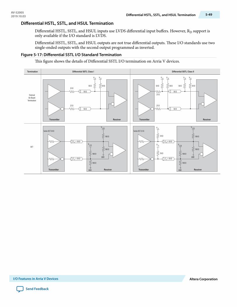
Differential HSTL, SSTL, and HSUL Termination
Differential HSTL, SSTL, and HSUL inputs use LVDS differential input buffers. However, RD support isonly available if the I/O standard is LVDS.
Differential HSTL, SSTL, and HSUL outputs are not true differential outputs. These I/O standards use twosingle-ended outputs with the second output programmed as inverted.
Figure 5-17: Differential SSTL I/O Standard TerminationThis figure shows the details of Differential SSTL I/O termination on Arria V devices.
Transmitter Receiver Transmitter Receiver
Series OCT 25 Ω
Transmitter Receiver
Series OCT 50 Ω
Transmitter Receiver
25 Ω
50 Ω
50 Ω
V TT
25 Ω
50 Ω
50 Ω
V TT
25 Ω
50 Ω
50 Ω
V TT
25 Ω50 Ω
50 Ω
V TT
50 Ω
V TT
50 Ω
V TT
50 Ω
V TT
100 Ω
100 Ω
GND
V CCIO
100 Ω
100 Ω
GND
V CCIO
50 Ω
V TT
100 Ω
100 Ω
GND
V CCIO
100 Ω
100 Ω
GND
V CCIO
Differential SSTL Class ITermination
OCT
Differential SSTL Class II
External On-Board
Termination
Z 0 = 50 Ω
Z 0 = 50 Ω
Z 0 = 50 Ω
Z 0 = 50 Ω
AV-520052019.10.03 Differential HSTL, SSTL, and HSUL Termination 5-49
I/O Features in Arria V Devices Altera Corporation
Send Feedback
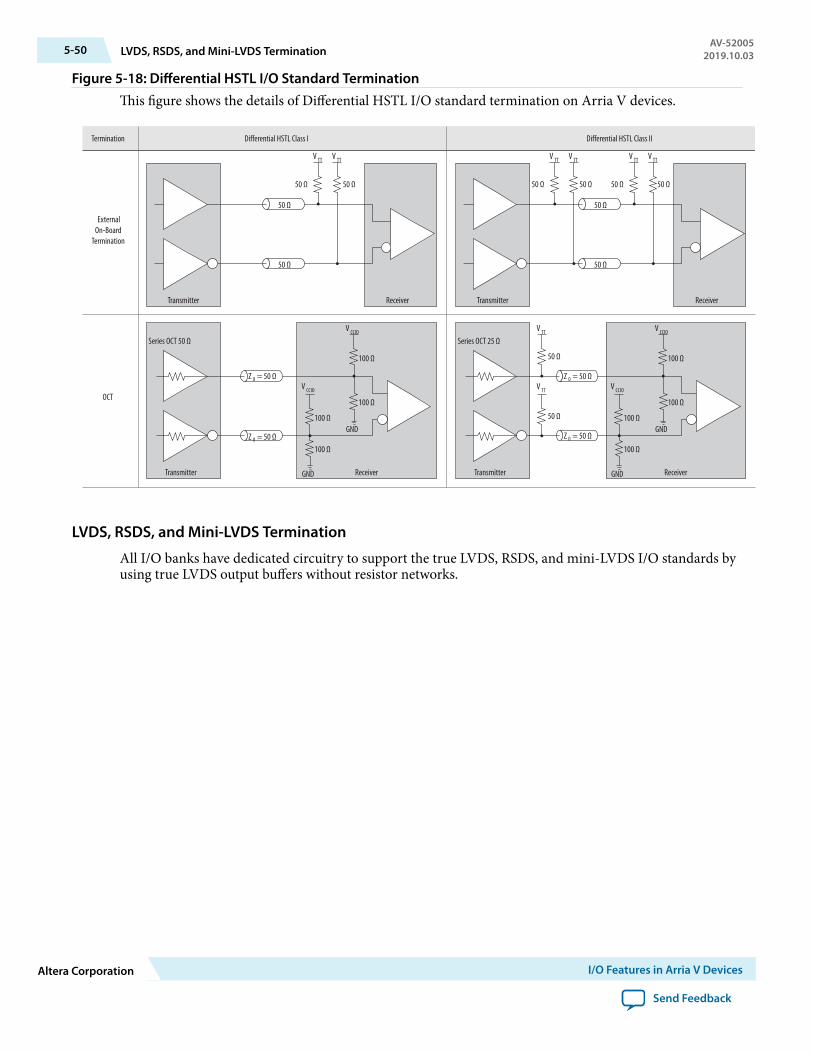
Figure 5-18: Differential HSTL I/O Standard TerminationThis figure shows the details of Differential HSTL I/O standard termination on Arria V devices.
Transmitter Receiver Transmitter Receiver
Series OCT 25 Ω
Transmitter Receiver
Series OCT 50 Ω
Transmitter Receiver
50 Ω
50 Ω
V TT
50 Ω
50 Ω
V TT
50 Ω
50 Ω
V TT
50 Ω
50 Ω
V TT
50 Ω
V TT
50 Ω
V TT
50 Ω
V TT
100 Ω
100 Ω
GND
V CCIO
100 Ω
100 Ω
GND
V CCIO
50 Ω
V TT
100 Ω
100 Ω
GND
V CCIO
100 Ω
100 Ω
GND
V CCIO
Differential HSTL Class ITermination
OCT
Differential HSTL Class II
External On-Board
Termination
Z 0 = 50 Ω
Z 0 = 50 Ω Z 0 = 50 Ω
Z 0 = 50 Ω
LVDS, RSDS, and Mini-LVDS Termination
All I/O banks have dedicated circuitry to support the true LVDS, RSDS, and mini-LVDS I/O standards byusing true LVDS output buffers without resistor networks.
5-50 LVDS, RSDS, and Mini-LVDS TerminationAV-52005
2019.10.03
Altera Corporation I/O Features in Arria V Devices
Send Feedback

Figure 5-19: LVDS I/O Standard TerminationThis figure shows the LVDS I/O standard termination. The on-chip differential resistor is available in allI/O banks.
Differential Outputs Differential Inputs
Differential Outputs Differential Inputs
50 Ω100 Ω
50 Ω
50 Ω100 Ω
50 Ω
LVDSTermination
Receiver
OCT
External On-Board
Termination
OCT Receiver (True LVDS
Output)
Emulated LVDS, RSDS, and Mini-LVDS Termination
The I/O banks also support emulated LVDS, RSDS, and mini-LVDS I/O standards.
Emulated LVDS, RSDS and mini-LVDS output buffers use two single-ended output buffers with anexternal single-resistor or three-resistor network, and can be tri-stated.
AV-520052019.10.03 Emulated LVDS, RSDS, and Mini-LVDS Termination 5-51
I/O Features in Arria V Devices Altera Corporation
Send Feedback
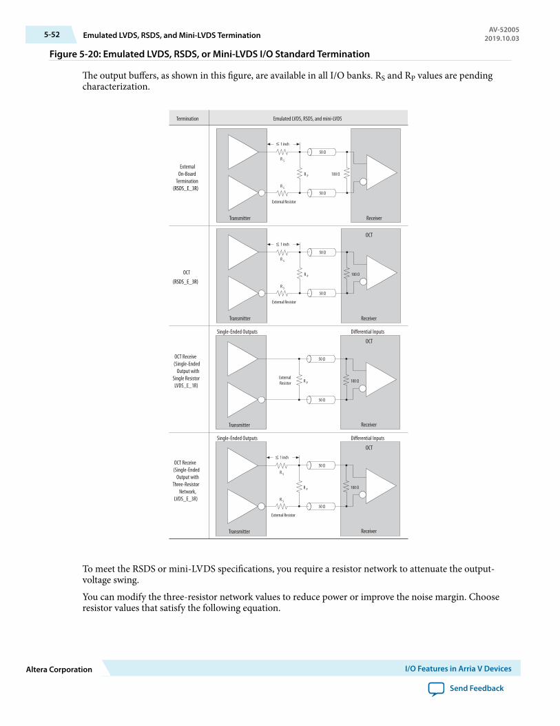
Figure 5-20: Emulated LVDS, RSDS, or Mini-LVDS I/O Standard Termination
The output buffers, as shown in this figure, are available in all I/O banks. RS and RP values are pendingcharacterization.
Receiver
OCT
Transmitter
ReceiverTransmitter
50 Ω
50 Ω
100 Ω
≤ 1 inch
External Resistor
R S
R S
R P
50 Ω
50 Ω
100 Ω
≤ 1 inch
External Resistor
R S
R S
R P
OCT
Emulated LVDS, RSDS, and mini-LVDSTermination
Single-Ended Outputs Differential Inputs
Transmitter
50 Ω
50 Ω
100 ΩExternal Resistor R P
Receiver
OCT
Single-Ended Outputs Differential Inputs
Transmitter
50 Ω
50 Ω
100 Ω
≤ 1 inch
External Resistor
R S
R S
R P
Receiver
OCT
(RSDS_E_3R)
ExternalOn-Board
Termination(RSDS_E_3R)
OCT Receive (Single-Ended
Output with Single Resistor LVDS_E_1R)
OCT Receive (Single-Ended
Output withThree-Resistor
Network, LVDS_E_3R)
To meet the RSDS or mini-LVDS specifications, you require a resistor network to attenuate the output-voltage swing.
You can modify the three-resistor network values to reduce power or improve the noise margin. Chooseresistor values that satisfy the following equation.
5-52 Emulated LVDS, RSDS, and Mini-LVDS TerminationAV-52005
2019.10.03
Altera Corporation I/O Features in Arria V Devices
Send Feedback
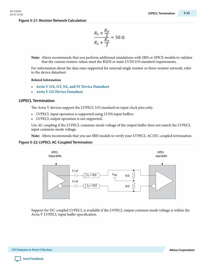
Figure 5-21: Resistor Network Calculation
Note: Altera recommends that you perform additional simulations with IBIS or SPICE models to validatethat the custom resistor values meet the RSDS or mini-LVDS I/O standard requirements.
For information about the data rates supported for external single resistor or three-resistor network, referto the device datasheet.
Related Information
• Arria V GX, GT, SX, and ST Device Datasheet• Arria V GZ Device Datasheet
LVPECL Termination
The Arria V devices support the LVPECL I/O standard on input clock pins only:
• LVPECL input operation is supported using LVDS input buffers.• LVPECL output operation is not supported.
Use AC coupling if the LVPECL common-mode voltage of the output buffer does not match the LVPECLinput common-mode voltage.
Note: Altera recommends that you use IBIS models to verify your LVPECL AC/DC-coupled termination.
Figure 5-22: LVPECL AC-Coupled Termination
Z 0 = 50 Ω V ICM
Z 0 = 50 Ω 50 Ω
50 Ω
0.1 µF
0.1 µF
LVPECLOutput Buffer
LVPECLInput Buffer
Support for DC-coupled LVPECL is available if the LVPECL output common mode voltage is within theArria V LVPECL input buffer specification.
AV-520052019.10.03 LVPECL Termination 5-53
I/O Features in Arria V Devices Altera Corporation
Send Feedback
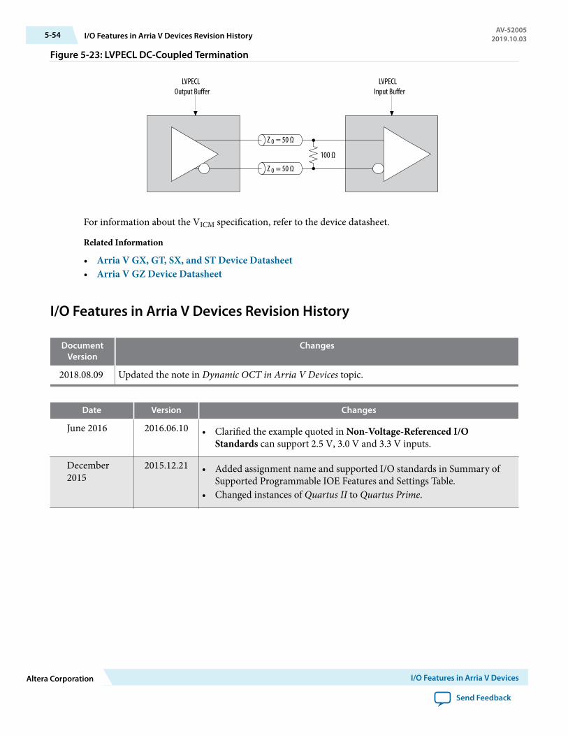
Figure 5-23: LVPECL DC-Coupled Termination
Z 0 = 50 Ω
Z 0 = 50 Ω
100 Ω
LVPECLOutput Buffer
LVPECLInput Buffer
For information about the VICM specification, refer to the device datasheet.
Related Information
• Arria V GX, GT, SX, and ST Device Datasheet• Arria V GZ Device Datasheet
I/O Features in Arria V Devices Revision History
DocumentVersion
Changes
2018.08.09 Updated the note in Dynamic OCT in Arria V Devices topic.
Date Version Changes
June 2016 2016.06.10 • Clarified the example quoted in Non-Voltage-Referenced I/OStandards can support 2.5 V, 3.0 V and 3.3 V inputs.
December2015
2015.12.21 • Added assignment name and supported I/O standards in Summary ofSupported Programmable IOE Features and Settings Table.
• Changed instances of Quartus II to Quartus Prime.
5-54 I/O Features in Arria V Devices Revision HistoryAV-52005
2019.10.03
Altera Corporation I/O Features in Arria V Devices
Send Feedback

Date Version Changes
January 215 2015.01.23 • Corrected truncated sentence in the note about the recommendationto use dynamic OCT for several I/O standards with DDR3 externalmemory interface.
• Added pin placement guidelines for general purpose high-speedsignals faster than 200 MHz.
• Added 3.3V to Arria V I/O Standards Voltage Levels table for 3.3VLVTTL/3.3V LVCMOS, 3.0V LVTTL/3.0V LVCMOS and 2.5VLVCMOS I/O Standard.
• Clarified that dedicated configuration pins, clock pins and JTAG pinsdo not support programmable pull-up resistor but these pins havefixed value of internal pull-up resistors.
• Moved the Open-Drain Output, Bus-Hold Circuitry and Pull-upResistor sections to Programmable IOE Features in Arria V Devices.
• Update Open-Drain Output section with steps to enable open-drainoutput in Assignment Editor.
June 2014 2014.06.30 • Added footnote to clarify that some of the voltage levels listed in theMultiVolt I/O support table are for showing that multiple single-ended I/O standards are not compatible with certain VCCIO voltages.
• Updated the I/O banks locations figures to match the availablemodular I/O banks for Arria V GX, GT, SX, and ST devices.
• Added information to clarify that programmable output slew rate isavailable for single-ended and emulated LVDS I/O standards.
• Finalized calibrated RS and RT OCT values and updated the RT OCTvalues for HSUL-12 and Differential HSUL-12 I/O standards.
• Updated the VCCPD guideline to clarify that bank 7A is not availableas user I/O bank. In Arria V SX and ST devices, banks 6A, 6B, and 7Athrough 7E are allocated for the HPS.
AV-520052019.10.03 I/O Features in Arria V Devices Revision History 5-55
I/O Features in Arria V Devices Altera Corporation
Send Feedback
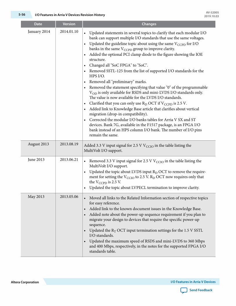
Date Version Changes
January 2014 2014.01.10 • Updated statements in several topics to clarify that each modular I/Obank can support multiple I/O standards that use the same voltages.
• Updated the guideline topic about using the same VCCPD for I/Obanks in the same VCCPD group to improve clarity.
• Added the optional PCI clamp diode to the figure showing the IOEstructure.
• Changed all "SoC FPGA" to "SoC".• Removed SSTL-125 from the list of supported I/O standards for the
HPS I/O.• Removed all "preliminary" marks.• Removed the statement specifying that value "0" of the programmable
VOD is only available for RSDS and mini-LVDS I/O standards only.The value is now available for the LVDS I/O standards.
• Clarified that you can only use RD OCT if VCCPD is 2.5 V.• Added link to Knowledge Base article that clarifies about vertical
migration (drop-in compatibility).• Corrected the modular I/O banks tables for Arria V SX and ST
devices. Bank 7G, available in the F1517 package, is an FPGA I/Obank instead of an HPS column I/O bank. The number of I/O pinsremain the same.
August 2013 2013.08.19 Added 3.3 V input signal for 2.5 V VCCIO in the table listing theMultiVolt I/O support.
June 2013 2013.06.21 • Removed 3.3 V input signal for 2.5 V VCCIO in the table listing theMultiVolt I/O support.
• Updated the topic about LVDS input RD OCT to remove the require‐ment for setting the VCCIO to 2.5 V. RD OCT now requires only thatthe VCCPD is 2.5 V.
• Updated the topic about LVPECL termination to improve clarity.
May 2013 2013.05.06 • Moved all links to the Related Information section of respective topicsfor easy reference.
• Added link to the known document issues in the Knowledge Base.• Added note about the power-up sequence requirement if you plan to
migrate your design to devices that require the specific power-upsequence.
• Updated the RT OCT input termination settings for the 1.5 V SSTLI/O standards.
• Updated the maximum speed of RSDS and mini-LVDS to 360 Mbpsand 400 Mbps, respectively, in the notes for the supported FPGA I/Ostandards table.
5-56 I/O Features in Arria V Devices Revision HistoryAV-52005
2019.10.03
Altera Corporation I/O Features in Arria V Devices
Send Feedback
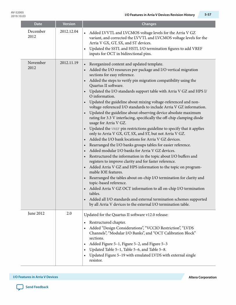
Date Version Changes
December2012
2012.12.04 • Added LVVTL and LVCMOS voltage levels for the Arria V GZvariant, and corrected the LVVTL and LVCMOS voltage levels for theArria V GX, GT, SX, and ST devices.
• Updated the SSTL and HSTL I/O termination figures to add VREFinputs for OCT in bidirectional pins.
November2012
2012.11.19 • Reorganized content and updated template.• Added the I/O resources per package and I/O vertical migration
sections for easy reference.• Added the steps to verify pin migration compatibility using the
Quartus II software.• Updated the I/O standards support table with Arria V GZ and HPS I/
O information.• Updated the guideline about mixing voltage-referenced and non-
voltage-referenced I/O standards to include Arria V GZ information.• Updated the guideline about observing device absolute maximum
rating for 3.3 V interfacing, specifically the off-chip clamping diodeusage for Arria V GZ.
• Updated the VREF pin restrictions guideline to specify that it appliesonly to Arria V GX, GT, SX, and ST, but not Arria V GZ.
• Added the I/O bank locations for Arria V GZ devices.• Rearranged the I/O banks groups tables for easier reference.• Added modular I/O banks for Arria V GZ devices.• Restructured the information in the topic about I/O buffers and
registers to improve clarity and for faster reference.• Added Arria V GZ and HPS information to the topic on program‐
mable IOE features.• Rearranged the tables about on-chip I/O termination for clarity and
topic-based reference.• Added Arria V GZ OCT information to all on-chip I/O termination
tables.• Added all I/O standards and external termination schemes supported
by all Arria V devices to the external I/O termination table.
June 2012 2.0 Updated for the Quartus II software v12.0 release:
• Restructured chapter.• Added “Design Considerations”, “VCCIO Restriction”, “LVDS
Channels”, “Modular I/O Banks”, and “OCT Calibration Block”sections.
• Added Figure 5–1, Figure 5–2, and Figure 5–3• Updated Table 5–1, Table 5–6, and Table 5–8.• Updated Figure 5–19 with emulated LVDS with external single
resistor.
AV-520052019.10.03 I/O Features in Arria V Devices Revision History 5-57
I/O Features in Arria V Devices Altera Corporation
Send Feedback
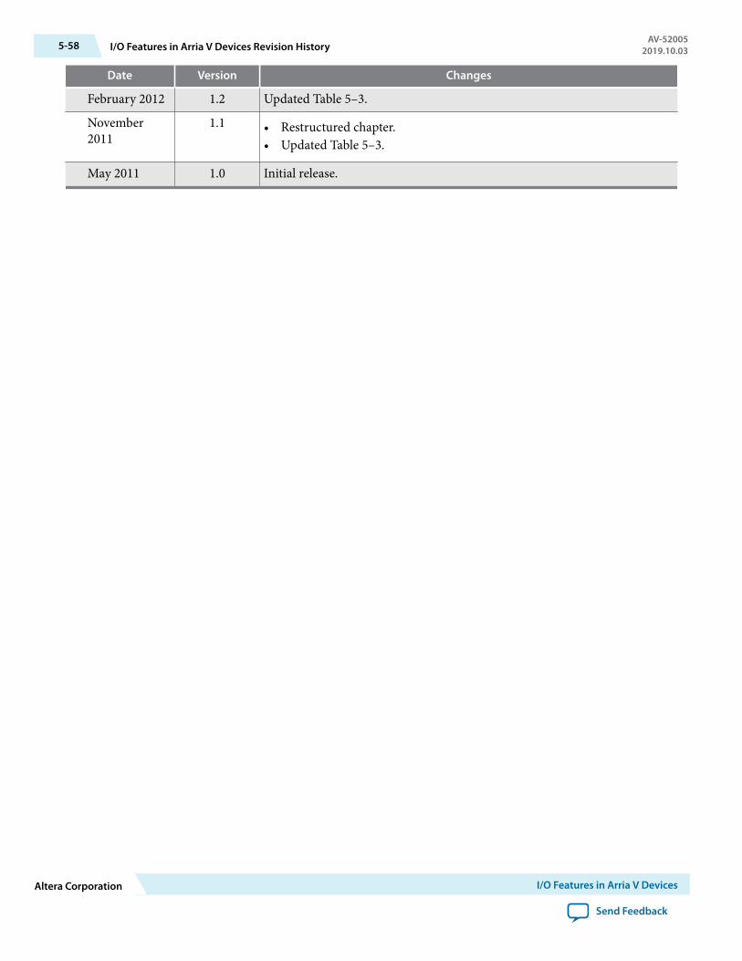
Date Version Changes
February 2012 1.2 Updated Table 5–3.
November2011
1.1 • Restructured chapter.• Updated Table 5–3.
May 2011 1.0 Initial release.
5-58 I/O Features in Arria V Devices Revision HistoryAV-52005
2019.10.03
Altera Corporation I/O Features in Arria V Devices
Send Feedback
High-Speed Differential I/O Interfaces and DPAin Arria V Devices 6
2019.10.03
AV-52006 Subscribe Send Feedback
The high-speed differential I/O interfaces and dynamic phase alignment (DPA) features in Arria V devicesprovide advantages over single-ended I/Os and contribute to the achievable overall system bandwidth.Arria V devices support low-voltage differential signaling (LVDS), mini-LVDS, and reduced swingdifferential signaling (RSDS) differential I/O standards.
The following figure shows the I/O bank support for high-speed differential I/O in the Arria V devices.
Figure 6-1: I/O Bank Support for High-Speed Differential I/O
LVDS I/Os
I/Os withDedicated
SERDES Circuitry
LVDS Interfacewith 'Use External PLL'
Option Disabled
LVDS Interfacewith 'Use External PLL'
Option Enabled
Related Information
• I/O Standards Support for FPGA I/O in Arria V Devices on page 5-6Provides information about the supported differential I/O standards.
• Arria V Device Handbook: Known IssuesLists the planned updates to the Arria V Device Handbook chapters.
Intel Corporation. All rights reserved. Intel, the Intel logo, Altera, Arria, Cyclone, Enpirion, MAX, Nios, Quartus and Stratix words and logos are trademarks ofIntel Corporation or its subsidiaries in the U.S. and/or other countries. Intel warrants performance of its FPGA and semiconductor products to currentspecifications in accordance with Intel's standard warranty, but reserves the right to make changes to any products and services at any time without notice.Intel assumes no responsibility or liability arising out of the application or use of any information, product, or service described herein except as expresslyagreed to in writing by Intel. Intel customers are advised to obtain the latest version of device specifications before relying on any published informationand before placing orders for products or services.*Other names and brands may be claimed as the property of others.
ISO9001:2015Registered
www.altera.com101 Innovation Drive, San Jose, CA 95134

Dedicated High-Speed Circuitries in Arria V DevicesThe following dedicated circuitries are available in the Arria V device family to support high-speeddifferential I/O:
• Differential I/O buffer• Transmitter serializer• Receiver deserializer• Data realignment (Bit-slip)• DPA• Synchronizer (FIFO buffer)• Phase-locked loops (PLLs)
SERDES and DPA Bank Locations in Arria V DevicesThe dedicated serializer/deserializer (SERDES) and DPA circuitry that supports high-speed differentialI/Os is located in the top and bottom banks of the Arria V devices.
The following figures show the high-level location of SERDES/DPA in the Arria V devices.
Figure 6-2: High-Speed Differential I/Os with DPA Locations in Arria V GX A1 and A3 Devices, and ArriaV GT C3 Device.
FPGA Fabric(Logic Elements, DSP,
Embedded Memory,Clock Networks)
General Purpose I/O
General Purpose I/O and High-SpeedLVDS I/O with DPA and Soft-CDR
Fractional PLL
Transceiver Block
6-2 Dedicated High-Speed Circuitries in Arria V DevicesAV-52006
2019.10.03
Altera Corporation High-Speed Differential I/O Interfaces and DPA in Arria V Devices
Send Feedback
Figure 6-3: High-Speed Differential I/Os with DPA Locations in Arria V GX A5, A7, B1, and B3 Devices, andArria V GT C7, D3, and D7 Devices
General Purpose I/O and High-SpeedLVDS I/O with DPA and Soft-CDR
Fractional PLL
Transceiver Block
FPGA Fabric(Logic Elements, DSP,
Embedded Memory,Clock Networks)
Figure 6-4: High-Speed Differential I/Os with DPA Locations in Arria V GX B5 and B7 Devices
General Purpose I/O and High-SpeedLVDS I/O with DPA and Soft-CDR
Fractional PLL
Transceiver Block
FPGA Fabric(Logic Elements, DSP,
Embedded Memory,Clock Networks)
Figure 6-5: High-Speed Differential I/Os with DPA Locations in Arria V GZ Devices
General Purpose I/O and High-SpeedLVDS I/O with DPA and Soft-CDR
Fractional PLL
Transceiver Block
FPGA Fabric(Logic Elements, DSP,
Embedded Memory,Clock Networks)
Left ClockRegion
Left ClockRegion
Right ClockRegion
Right ClockRegion
Related InformationPLLs and Clocking for Arria V Devices on page 6-7
AV-520062019.10.03 SERDES and DPA Bank Locations in Arria V Devices 6-3
High-Speed Differential I/O Interfaces and DPA in Arria V Devices Altera Corporation
Send Feedback

LVDS SERDES CircuitryThe Arria V devices have built-in serializer/deserializer (SERDES) circuitry that supports high-speedLVDS interfaces. You can configure the SERDES circuitry to support source-synchronous communicationprotocols such as RapidIO®, XSBI, serial peripheral interface (SPI), and asynchronous protocols such asGigabit Ethernet (GbE).
The following figure shows a transmitter and receiver block diagram for the LVDS SERDES circuitry withthe interface signals of the transmitter and receiver data paths.
Figure 6-6: LVDS SERDES
rx_in
tx_out
DPA CircuitrySynchronizerBit SlipDeserializer
rx_inclock / tx_inclock
IOE supports SDR, DDR, or non-registered datapath
IOE supports SDR, DDR, or non-registered datapath
LVDS Receiver
LVDS Transmitter
FPGAFabric
rx_out
tx_in
rx_divfwdclkrx_outclock
tx_coreclock
Serializer
DPA Clock DomainLVDS Clock Domain
RetimedData
DPA Clock
DINDOUT DINDOUT DINDOUT DIN
DIN DOUT
Clock Mux
Fractional PLL
IOE
+–
+–
IOE
LVDS
_diff
ioclk
DPA_
diffio
clk(LOAD_EN,diffioclk)
(DPA_LOAD_EN, DPA_diffioclk, rx_divfwdclk)
2
2
3
3
10
10
10
(LVDS_LOAD_EN, diffioclk, tx_coreclock)
3 (LVDS_LOAD_EN,LVDS_diffioclk, rx_outclock) 8 Serial LVDS
Clock Phases
2
diffioclk
10 bitsmaxiumumdata width
The preceding figure shows a shared PLL between the transmitter and receiver. If the transmitter andreceiver do not share the same PLL, you require two fractional PLLs. In single data rate (SDR) and doubledata rate (DDR) modes, the data width is 1 and 2 bits, respectively.
The ALTLVDS transmitter and receiver requires various clock and load enable signals from a fractionalPLL. The Intel Quartus Prime software configures the PLL settings automatically. The software is alsoresponsible for generating the various clock and load enable signals based on the input reference clock andselected data rate.
Note: For the maximum data rate supported by the Arria V devices, refer to the device overview.
Related Information
• Arria V Device Overview
6-4 LVDS SERDES CircuitryAV-52006
2019.10.03
Altera Corporation High-Speed Differential I/O Interfaces and DPA in Arria V Devices
Send Feedback
• LVDS SERDES Transmitter/Receiver IP Cores User GuideProvides a list of the LVDS transmitter and receiver ports and settings using ALTLVDS.
• Guideline: Use PLLs in Integer PLL Mode for LVDS on page 6-8
True LVDS Buffers in Arria V DevicesThe following tables list the number of true LVDS buffers supported in Arria V devices with theseconditions:
• The LVDS channel count does not include dedicated clock pins.• Dedicated SERDES and DPA is available for top and bottom banks only.• Each I/O sub-bank can support up to two independent ALTLVDS interfaces. For example, you can
place two ALTLVDS interfaces in bank 8A driven by two different PLLs, provided that the LVDSchannels are not interleaved.
Table 6-1: LVDS Channels Supported in Arria V GX Devices
Member Code Package Side TX RX
A1 and A3672-pin FineLine BGA, Flip Chip
Top 28 34Bottom 29 34
896-pin FineLine BGA, Flip ChipTop 33 40
Bottom 34 40
A5 and A7
672-pin FineLine BGA, Flip ChipTop 34 44
Bottom 34 44
896-pin FineLine BGA, Flip ChipTop 42 48
Bottom 42 48
1152-pin FineLine BGA, FlipChip
Top 60 68Bottom 60 68
B1 and B3
896-pin FineLine BGA, Flip ChipTop 42 48
Bottom 42 48
1152-pin FineLine BGA, FlipChip
Top 60 68Bottom 60 68
1517-pin FineLine BGA, FlipChip
Top 80 88Bottom 80 88
B5 and B7
1152-pin FineLine BGA, FlipChip
Top 60 68Bottom 60 68
1517-pin FineLine BGA, FlipChip
Top 80 88Bottom 80 88
AV-520062019.10.03 True LVDS Buffers in Arria V Devices 6-5
High-Speed Differential I/O Interfaces and DPA in Arria V Devices Altera Corporation
Send Feedback

Table 6-2: LVDS Channels Supported in Arria V GT Devices
Member Code Package Side TX RX
C3672-pin FineLine BGA, Flip Chip
Top 26 34Bottom 26 34
896-pin FineLine BGA, Flip ChipTop 34 40
Bottom 34 40
C7896-pin FineLine BGA, Flip Chip
Top 42 48Bottom 42 48
1152-pin FineLine BGA, FlipChip
Top 60 68Bottom 60 68
D3
896-pin FineLine BGA, Flip ChipTop 42 48
Bottom 42 48
1152-pin FineLine BGA, FlipChip
Top 60 68Bottom 60 68
1517-pin FineLine BGA, FlipChip
Top 80 88Bottom 80 88
D7
1152-pin FineLine BGA, FlipChip
Top 60 68Bottom 60 68
1517-pin FineLine BGA, FlipChip
Top 80 88Bottom 80 88
Table 6-3: LVDS Channels Supported in Arria V GZ Devices
Member Code Package Side TX RX
E1 and E3780-pin FineLine BGA, Flip Chip
Top 42 51Bottom 39 39
1152-pin FineLine BGA, FlipChip
Top 48 57Bottom 51 51
E5 and E7
1152-pin FineLine BGA, FlipChip
Top 54 63Bottom 75 75
1517-pin FineLine BGA, FlipChip
Top 79 81Bottom 87 87
6-6 True LVDS Buffers in Arria V DevicesAV-52006
2019.10.03
Altera Corporation High-Speed Differential I/O Interfaces and DPA in Arria V Devices
Send Feedback

Table 6-4: LVDS Channels Supported in Arria V SX Devices
Member Code Package Side TX RX
B3 and B5
896-pin FineLine BGA, Flip ChipTop 14 37
Bottom 20 37
1152-pin FineLine BGA, FlipChip
Top 14 37Bottom 30 77
1517-pin FineLine BGA, FlipChip
Top 40 48Bottom 80 88
Table 6-5: LVDS Channels Supported in Arria V ST Devices
Member Code Package Side TX RX
D3 and D5
896-pin FineLine BGA, Flip ChipTop 14 37
Bottom 20 37
1152-pin FineLine BGA, FlipChip
Top 14 37Bottom 30 77
1517-pin FineLine BGA, FlipChip
Top 40 48Bottom 80 88
Emulated LVDS Buffers in Arria V DevicesThe Arria V device family supports emulated LVDS:
• You can use unutilized true LVDS input channels as emulated LVDS output buffers (eTX) for serializa‐tion factors of 1 and 2.
• The emulated differential output buffers support tri-state capability.
High-Speed I/O Design Guidelines for Arria V DevicesThere are several considerations that require your attention to ensure the success of your designs. Unlessnoted otherwise, these design guidelines apply to all variants of this device family.
PLLs and Clocking for Arria V DevicesTo generate the parallel clocks (rx_outclock and tx_outclock) and high-speed clocks (diffioclk), theArria V devices provide fractional PLLs in the high-speed differential I/O receiver and transmitterchannels.
Related Information
• Guideline: Use PLLs in Integer PLL Mode for LVDS on page 6-8• SERDES and DPA Bank Locations in Arria V Devices on page 6-2
Provides information about the PLL locations available for each Arria V device.• Guideline: Use High-Speed Clock from PLL to Clock LVDS SERDES Only on page 6-8
AV-520062019.10.03 Emulated LVDS Buffers in Arria V Devices 6-7
High-Speed Differential I/O Interfaces and DPA in Arria V Devices Altera Corporation
Send Feedback

Guideline: Use PLLs in Integer PLL Mode for LVDS
To drive the LVDS channels, you must use the PLLs in integer PLL mode. The center or corner PLLs candrive the LVDS receiver and transmitter channels.
However, in Arria V GZ devices, the clock tree network cannot cross over to different I/O regions. Forexample, the top left corner PLL cannot cross over to drive the LVDS receiver and transmitter channels onthe top right I/O bank.
Related InformationPin Placement Guidelines for DPA and Non-DPA Differential Channels on page 6-13Provides more information about the fractional PLL clocking restrictions.
Guideline: Use High-Speed Clock from PLL to Clock LVDS SERDES Only
The high-speed clock generated from the PLL is intended to clock the LVDS SERDES circuitry only. Donot use the high-speed clock to drive other logic because the allowed frequency to drive the core logic isrestricted by the PLL FOUT specification.
For more information about the FOUT specification, refer to the device datasheet.
Note: Spread-spectrum input clock is not supported in LVDS.
LVDS Interface with External PLL ModeThe IP Catalog provides an option for implementing the LVDS interface with the Use External PLLoption. With this option enabled you can control the PLL settings, such as dynamically reconfiguring thePLL to support different data rates, dynamic phase shift, and other settings. You must also instantiate thean Altera_PLL IP core to generate the various clock and load enable signals.
If you enable the Use External PLL option with the ALTLVDS transmitter and receiver, the followingsignals are required from the Altera_PLL IP core:
• Serial clock input to the SERDES of the ALTLVDS transmitter and receiver• Load enable to the SERDES of the ALTLVDS transmitter and receiver• Parallel clock used to clock the transmitter FPGA fabric logic and parallel clock used for the receiver• Asynchronous PLL reset port of the ALTLVDS receiver
Altera_PLL Signal Interface with ALTLVDS IP Core
Table 6-6: Signal Interface Between Altera_PLL and ALTLVDS IP Cores
This table lists the signal interface between the output ports of the Altera_PLL IP core and the input portsof the ALTLVDS transmitter and receiver. As an example, the table lists the serial clock output, load enableoutput, and parallel clock output generated on ports outclk0, outclk1, and outclk2, along with the lockedsignal of the Altera_PLL instance. You can choose any of the PLL output clock ports to generate theinterface clocks.
6-8 Guideline: Use PLLs in Integer PLL Mode for LVDSAV-52006
2019.10.03
Altera Corporation High-Speed Differential I/O Interfaces and DPA in Arria V Devices
Send Feedback

From the Altera_PLL IP Core To the ALTLVDS Transmitter To the ALTLVDS Receiver
Serial clock output(outclk0)
The serial clock output(outclk0) can only drivetx_inclock on theALTLVDS transmitter, andrx_inclock and rx_dpaclock on the ALTLVDSreceiver. This clock cannotdrive the core logic.
tx_inclock (serial clock inputto the transmitter)
rx_inclock (serial clock input)
rx_dpaclock
Load enable output(outclk1)
tx_enable (load enable to thetransmitter)
rx_enable (load enable for the deserializer)
Parallel clock output(outclk2)
Parallel clock used inside thetransmitter core logic in theFPGA fabric
rx_syncclock (parallel clock input) andparallel clock used inside the receiver corelogic in the FPGA fabric
~(locked) — pll_areset (asynchronous PLL reset port)
The pll_areset signal is automaticallyenabled for the LVDS receiver in externalPLL mode. This signal does not exist forLVDS transmitter instantiation when theexternal PLL option is enabled.
Note: With soft SERDES, a different clocking requirement is needed.
Related InformationLVDS SERDES Transmitter/Receiver IP Cores User GuideMore information about the different clocking requirement for soft SERDES.
Altera_PLL Parameter Values for External PLL Mode
The following examples show the clocking requirements to generate output clocks for ALTLVDS_TX andALTLVDS_RX using the Altera_PLL IP core. The examples set the phase shift with the assumption thatthe clock and data are edge aligned at the pins of the device.
Note: For other clock and data phase relationships, Altera recommends that you first instantiate yourALTLVDS_RX and ALTLVDS_TX interface without using the external PLL mode option. Compilethe IP cores in the Intel Quartus Prime software and take note of the frequency, phase shift, andduty cycle settings for each clock output. Enter these settings in the Altera_PLL IP core parametereditor and then connect the appropriate output to the ALTLVDS_RX and ALTLVDS_TX IP cores.
Table 6-7: Example: Generating Output Clocks Using an Altera_PLL IP Core (No DPA and Soft-CDR Mode)
This table lists the parameter values that you can set in the Altera_PLL parameter editor to generate threeoutput clocks using an Altera_PLL IP core if you are not using DPA and soft-CDR mode.
AV-520062019.10.03 Altera_PLL Parameter Values for External PLL Mode 6-9
High-Speed Differential I/O Interfaces and DPA in Arria V Devices Altera Corporation
Send Feedback
Parameter outclk0
(Connects to the tx_inclockport of ALTLVDS_TX and therx_inclock port of ALTLVDS_
RX)
outclk1
(Connects to the tx_enableport of ALTLVDS_TX and therx_enable port of ALTLVDS_
RX)
outclk2
(Used as the core clock for theparallel data registers for bothtransmitter and receiver, andconnects to the rx_synclock
port of ALTLVDS_RX)
Frequency data rate data rate/serialization factor data rate/serializationfactor
Phase shift –180° [(deserialization factor – 2)/deserialization factor] x 360°
–180/serialization factor
(outclk0 phase shift dividedby the serialization factor)
Duty cycle 50% 100/serialization factor 50%
Figure 6-7: Phase Relationship for External PLL Interface Signals
D1 D2 D3 D4 D5 D6 D7 D8 D9 D10
inclk0
RX serial data
D1 D2 D3 D4 D5 D6 D7 D8 D9 D10TX serial data
VCO clk(internal PLL clk)
outclk0(-180° phase shift)
outclk1(288° phase shift)
outclk2(-18° phase shift)
tx_outclk
Table 6-8: Example: Generating Output Clocks Using an Altera_PLL IP Core (With DPA and Soft-CDR Mode)
This table lists the parameter values that you can set in the Altera_PLL parameter editor to generate fouroutput clocks using an Altera_PLL IP core if you are using DPA and soft-CDR mode. The locked outputport of Altera_PLL must be inverted and connected to the pll_areset port of the ALTLVDS_RX IP coreif you are using DPA and soft-CDR mode.
6-10 Altera_PLL Parameter Values for External PLL ModeAV-52006
2019.10.03
Altera Corporation High-Speed Differential I/O Interfaces and DPA in Arria V Devices
Send Feedback
Parameter outclk0
(Connects to the tx_inclock port of
ALTLVDS_TX and therx_inclock port of
ALTLVDS_RX)
outclk1
(Connects to the tx_enable port of
ALTLVDS_TX and therx_enable port of
ALTLVDS_RX)
outclk2
(Used as the core clockfor the parallel data
registers for bothtransmitter and
receiver, and connectsto the rx_synclockport of ALTLVDS_RX)
outclk3
(Connects to the rx_dpaclock port of
ALTLVDS_RX)
Frequency
data rate data rate/serializationfactor
data rate/serializationfactor
data rate
Phaseshift
–180° [(deserialization factor- 2)/deserializationfactor] x 360°
–180/serializationfactor
(outclk0 phase shiftdivided by the serializa‐tion factor)
–180°
Dutycycle
50% 100/serialization factor 50% 50%
Connection between Altera_PLL and ALTLVDS
Figure 6-8: LVDS Interface with the Altera_PLL IP Core (Without DPA and Soft-CDR Mode)
This figure shows the connections between the Altera_PLL and ALTLVDS IP core if you are not usingDPA and soft-CDR mode.
D Q
DQ
TransmitterCore Logic
tx_coreclk
LVDS Transmitter(ALTLVDS)
LVDS Receiver(ALTLVDS)
rx_inclockReceiverCore Logic
rx_coreclk
rx_enablerx_syncclock
pll_areset
rx_out
tx_inclock
tx_enable
tx_in
Altera_PLL
inclk0
pll_areset
outclk0
outclk2outclk1
locked
FPGA Fabric
AV-520062019.10.03 Connection between Altera_PLL and ALTLVDS 6-11
High-Speed Differential I/O Interfaces and DPA in Arria V Devices Altera Corporation
Send Feedback
Figure 6-9: LVDS Interface with the Altera_PLL IP Core (With DPA)
This figure shows the connections between the Altera_PLL and ALTLVDS IP core if you are using DPA.The locked output port must be inverted and connected to the pll_areset port.
D Q
DQ
TransmitterCore Logic
tx_coreclk
LVDS Transmitter(ALTLVDS)
LVDS Receiver(ALTLVDS)
rx_inclockReceiverCore Logic
rx_coreclk
rx_dpaclockrx_enable
rx_syncclockpll_areset
rx_out
tx_inclock
tx_enable
tx_in
Altera_PLL
inclk0
pll_areset
outclk0
outclk2outclk3
outclk1
locked
FPGA Fabric
Figure 6-10: LVDS Interface with the Altera_PLL IP Core (With Soft-CDR Mode)
This figure shows the connections between the Altera_PLL and ALTLVDS IP core if you are using soft-CDR mode. The locked output port must be inverted and connected to the pll_areset port.
D Q
DQ
TransmitterCore Logic
tx_coreclk
LVDS Transmitter(ALTLVDS)
LVDS Receiver(ALTLVDS)
ReceiverCore Logic
rx_coreclk
rx_dpaclock
rx_syncclockpll_areset
rx_outrx_divfwdclk
tx_inclock
tx_enable
tx_in
Altera_PLL
inclk0
pll_areset
outclk0
outclk2outclk3
outclk1
locked
FPGA Fabric
rx_enable
rx_inclock
When generating the Altera_PLL IP core, the Left/Right PLL option is configured to set up the PLL inLVDS mode. Instantiation of pll_areset is optional.
The rx_enable and rx_inclock input ports are not used and can be left unconnected.
6-12 Connection between Altera_PLL and ALTLVDSAV-52006
2019.10.03
Altera Corporation High-Speed Differential I/O Interfaces and DPA in Arria V Devices
Send Feedback

Pin Placement Guidelines for DPA and Non-DPA Differential ChannelsDPA usage adds some constraints on the placement of high-speed differential channels. If DPA-enabled orDPA-disabled differential channels(22) in the differential banks are used, you must adhere to the differentialpin placement guidelines to ensure the proper high-speed operation. The Intel Quartus Prime compilerautomatically checks the design and issues an error message if the guidelines are not followed.
Note: The figures in this section show guidelines for using corner and center PLLs but do not necessarilyrepresent the exact locations of the high-speed LVDS I/O banks.
Related InformationGuideline: Use PLLs in Integer PLL Mode for LVDS on page 6-8
Guideline: Using DPA-Enabled Differential Channels
Each differential receiver in an I/O block has a dedicated DPA circuit to align the phase of the clock to thedata phase of its associated channel. If you enable a DPA channel in a bank, you can use both single-endedI/Os and differential I/O standards in the bank.
You can place double data rate I/O (DDIO) output pins within I/O modules that have the same pad groupnumber as a SERDES differential channel. However, you cannot place SDR I/O output pins within I/Omodules that have the same pad group number as a receiver SERDES differential channel. You mustimplement the input register within the FPGA fabric logic.
The following figure illustrates the clock network for DPA and SERDES resources in Arria V devices.
(22) DPA-enabled differential channels refer to DPA mode or soft-CDR mode while DPA disabled channels referto non-DPA mode.
AV-520062019.10.03 Pin Placement Guidelines for DPA and Non-DPA Differential Channels 6-13
High-Speed Differential I/O Interfaces and DPA in Arria V Devices Altera Corporation
Send Feedback

Figure 6-11: LVDS and DPA Clock Network
RX
TX
RX
TX
RX
TX
RX
TX
RX
TX
RX
TX
RX
TX
RX
TX
RX
TX
RX
TX
RX
TX
RX
TX
RX
TX
fPLL fPLL fPLL fPLL fPLL fPLL
DPA Clock Tree (8 VCO phase taps)
LVDS_diffioclk (0)
LVDS_diffioclk (1)
LVDS_LOAD_EN(0)
LVDS_LOAD_EN(1)
Interconnect between dedicated clock trees and SERDES TX & RX
Dedicated clock “stripes”span the entire edge of the device
Clock “stripes” are shared by corner and center fPLLs
IO BANK
Left Corner PLLs Right Corner PLLsCenter PLLs
If you use DPA-enabled channels in differential banks, adhere to the following guidelines.
Using Center and Corner PLLs
If two PLLs drive the DPA-enabled channels in a bank—the corner and center PLL drive one group each—there must be at least one row (one differential channel) of separation between the two groups of DPA-enabled channels, as shown in the following figure.
6-14 Guideline: Using DPA-Enabled Differential ChannelsAV-52006
2019.10.03
Altera Corporation High-Speed Differential I/O Interfaces and DPA in Arria V Devices
Send Feedback
Figure 6-12: Center and Corner PLLs Driving DPA-enabled Differential I/Os in the Same Bank
Diff I/OReference CLK
Channels Driven by Corner fPLLs
One Unused Channel for Buffer
Channels Driven by Center fPLLs
Center fPLL
TX & RXDPA-enabled
Diff I/O
TX & RXDPA-enabled
Diff I/O
TX & RXDPA-enabled
Diff I/O
TX & RX DPA-enabled
Diff I/O
RightCorner fPLL
Center fPLL
Reference CLK
TX & RXDPA-enabled
Diff I/O
TX & RXDPA-enabled
Diff I/O
Reference CLK
TX & RXDPA-enabled
Diff I/O
TX & RXDPA-enabled
Diff I/O
Non DPA-enabled
Diff I/O
Non DPA-enabled
Diff I/O
Reference CLK
RightCorner fPLL
This separation prevents noise mixing because the two groups can operate at independent frequencies. Noseparation is necessary if a single PLL is driving both the DPA-enabled channels and DPA-disabledchannels.
Using Both Center PLLs
You can use center PLLs to drive DPA-enabled channels simultaneously, if they drive these channels intheir adjacent banks only, as shown in the previous figure. If one of the center PLLs drives the DPA-enabled channels in the left and right I/O banks in Arria V GX, GT, SX, or ST devices, you cannot use theother center PLL for DPA-enabled channels. If the center left PLL drives the DPA-enabled channels in theright I/O bank, the right center PLL cannot drive the DPA-enabled channels in the left I/O bank, and viceversa. The center PLLs cannot drive cross-banks simultaneously in Arria V GZ devices. Refer to thefollowing figures.
AV-520062019.10.03 Guideline: Using DPA-Enabled Differential Channels 6-15
High-Speed Differential I/O Interfaces and DPA in Arria V Devices Altera Corporation
Send Feedback

Figure 6-13: Center PLLs Driving DPA-enabled Differential I/Os in Arria V GX, GT, SX, and ST Devices
DPA-enabled Diff I/O
Reference CLK
Center PLL
Center PLL
Reference CLK
DPA-enabled Diff I/O
DPA-enabled Diff I/O
DPA-enabled Diff I/O
DPA-enabled Diff I/O
DPA-enabled Diff I/O
DPA-enabled Diff I/O
DPA-enabled Diff I/O
Unused PLL
DPA-enabled Diff I/O
Reference CLK
Center PLL
Center PLL
Reference CLK
DPA-enabled Diff I/O
DPA-enabled Diff I/O
DPA-enabled Diff I/O
DPA-enabled Diff I/O
DPA-enabled Diff I/O
DPA-enabled Diff I/O
DPA-enabled Diff I/O
6-16 Guideline: Using DPA-Enabled Differential ChannelsAV-52006
2019.10.03
Altera Corporation High-Speed Differential I/O Interfaces and DPA in Arria V Devices
Send Feedback

Figure 6-14: Center PLLs Driving DPA-enabled Differential I/Os in Arria V GZ Devices
DPA-enabled Diff I/O
Reference CLK
Center PLL
Center PLL
Reference CLK
DPA-enabled Diff I/O
DPA-enabled Diff I/O
DPA-enabled Diff I/O
DPA-enabled Diff I/O
DPA-enabled Diff I/O
DPA-enabled Diff I/O
DPA-enabled Diff I/O
Figure 6-15: Invalid Placement of DPA-enabled Differential I/Os Driven by Both Center PLLs
DPA-enabled Diff I/O
Reference CLK
Center PLL
Center PLL
Reference CLK
DPA-enabled Diff I/O
DPA-enabled Diff I/O
DPA-enabled Diff I/O
DPA-enabled Diff I/O
DPA-enabled Diff I/O
DPA-enabled Diff I/O
DPA-enabled Diff I/O
Using Both Corner PLLs
You can use the left and right corner PLLs to drive DPA-enabled channels simultaneously, if they drive thechannels in their adjacent banks only. There must be at least one row of separation between the two groupsof DPA-enabled channels.
There are two PLL in each corner of the device. However, only one corner PLL can be use to drive DPA-enabled channels in a quadrant.
AV-520062019.10.03 Guideline: Using DPA-Enabled Differential Channels 6-17
High-Speed Differential I/O Interfaces and DPA in Arria V Devices Altera Corporation
Send Feedback
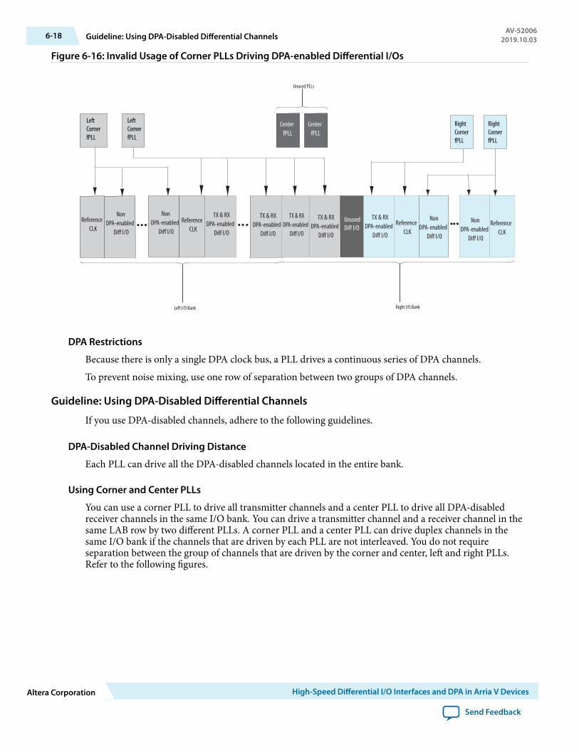
Figure 6-16: Invalid Usage of Corner PLLs Driving DPA-enabled Differential I/Os
TX & RXDPA-enabled
Diff I/O
Left I/O Bank
Unused PLLs
Right I/O Bank
Center fPLL
Center fPLL
Left Corner fPLL
Reference CLK
TX & RXDPA-enabled
Diff I/O
TX & RXDPA-enabled
Diff I/O
Non DPA-enabled
Diff I/O
Non DPA-enabled
Diff I/O
Reference CLK
UnusedDiff I/O
Reference CLK
Non DPA-enabled
Diff I/O
Non DPA-enabled
Diff I/O
Reference CLK
TX & RXDPA-enabled
Diff I/O
Left Corner fPLL
RightCorner fPLL
RightCorner fPLL
TX & RXDPA-enabled
Diff I/O
DPA Restrictions
Because there is only a single DPA clock bus, a PLL drives a continuous series of DPA channels.
To prevent noise mixing, use one row of separation between two groups of DPA channels.
Guideline: Using DPA-Disabled Differential Channels
If you use DPA-disabled channels, adhere to the following guidelines.
DPA-Disabled Channel Driving Distance
Each PLL can drive all the DPA-disabled channels located in the entire bank.
Using Corner and Center PLLs
You can use a corner PLL to drive all transmitter channels and a center PLL to drive all DPA-disabledreceiver channels in the same I/O bank. You can drive a transmitter channel and a receiver channel in thesame LAB row by two different PLLs. A corner PLL and a center PLL can drive duplex channels in thesame I/O bank if the channels that are driven by each PLL are not interleaved. You do not requireseparation between the group of channels that are driven by the corner and center, left and right PLLs.Refer to the following figures.
6-18 Guideline: Using DPA-Disabled Differential ChannelsAV-52006
2019.10.03
Altera Corporation High-Speed Differential I/O Interfaces and DPA in Arria V Devices
Send Feedback

Figure 6-17: Corner and Center PLLs Driving DPA-Disabled Differential I/Os in the Same Bank
DPA-disabledDiff TX & RX
Reference CLK
Center PLL
Corner PLL
Reference CLK
DPA-disabledDiff TX & RX
DPA-disabledDiff TX & RX
DPA-disabledDiff TX & RX
DPA-disabledDiff TX & RX
DPA-disabledDiff TX & RX
DPA-disabledDiff TX & RX
DPA-disabledDiff TX & RX
DPA-disabledDiff TX & RX
DPA-disabledDiff TX & RX
UnusedCorner
PLL
UnusedCenter
PLL
Channels Driven by Center fPLL
Channels Driven by Corner fPLL
No Separation Buffer Needed
Reference CLK
Center PLL
Corner PLL
Reference CLK
DPA-disabledDiff RX
DPA-disabledDiff RX
DPA-disabledDiff RX
DPA-disabledDiff RX
DPA-disabledDiff RX
UnusedCorner
PLL
UnusedCenter
PLL
Diff TX Diff TX Diff TX Diff TX Diff TX Diff TX Diff TXDiff TXDiff TXDiff TX
DPA-disabledDiff RX
DPA-disabledDiff RX
DPA-disabledDiff RX
DPA-disabledDiff RX
DPA-disabledDiff RX
AV-520062019.10.03 Guideline: Using DPA-Disabled Differential Channels 6-19
High-Speed Differential I/O Interfaces and DPA in Arria V Devices Altera Corporation
Send Feedback
Figure 6-18: Invalid Placement of DPA-disabled Differential I/Os Due to Interleaving of Channels Driven bythe Corner and Center PLLs
DPA-disabledDiff TX & RX
Reference CLK
Center PLL
Corner PLL
Reference CLK
DPA-disabledDiff TX & RX
DPA-disabledDiff TX & RX
DPA-disabledDiff TX & RX
DPA-disabledDiff TX & RX
DPA-disabledDiff TX & RX
DPA-disabledDiff TX & RX
DPA-disabledDiff TX & RX
DPA-disabledDiff TX & RX
DPA-disabledDiff TX & RX
UnusedCorner
PLL
UnusedCenter
PLL
Using Both Center PLLs
You can use both center PLLs simultaneously to drive DPA-disabled channels on left and right I/O banks.Unlike DPA-enabled channels, the center PLLs can drive DPA-disabled channels cross-banks in the ArriaV GX, GT, SX, and ST devices. For example, the left center PLL can drive the right I/O bank at the sametime the right center PLL is driving the left I/O bank, and vice versa, as shown in the following figure.
Note: In the Arria V GZ devices, the center PLLs cannot drive DPA-disabled channels cross-banks.
Figure 6-19: Both Center PLLs Driving Cross-Bank DPA-Disabled Channels Simultaneously in Arria V GX, GT,SX, and ST Devices
DPA-disabled Diff TX & RX
Reference CLK
Center PLL
Reference CLK
DPA-disabled Diff TX & RX
DPA-disabled Diff TX & RX
DPA-disabled Diff TX & RX
DPA-disabled Diff TX & RX
DPA-disabled Diff TX & RX
DPA-disabled Diff TX & RX
DPA-disabled Diff TX & RX
Center PLL
6-20 Guideline: Using DPA-Disabled Differential ChannelsAV-52006
2019.10.03
Altera Corporation High-Speed Differential I/O Interfaces and DPA in Arria V Devices
Send Feedback
Using Both Corner PLLs
You can use both corner PLLs to drive DPA-disabled channels simultaneously. You can use a corner PLL todrive all the transmitter channels and the other corner PLL to drive all the DPA-disabled receiver channelsin the same I/O bank. Both corner PLLs can drive duplex channels in the same I/O bank if the channelsthat are driven by each PLL are not interleaved. You do not require separation between the groups ofchannels that are driven by both corner PLLs.
Figure 6-20: Right Corner PLLs Driving LVDS Differential I/Os in the Same Bank
Corner PLL
Reference CLK
Reference CLK
DPA-disabledDiff RX
Diff TX Diff TX DPA-disabledDiff RX
Diff TX
CornerPLL
DPA-disabledDiff RX
Differential Transmitter in Arria V DevicesThe Arria V transmitter contains dedicated circuitry to support high-speed differential signaling. Thedifferential transmitter buffers support the following features:
• LVDS signaling that can drive out LVDS, mini-LVDS, and RSDS signals• Programmable VOD and programmable pre-emphasis
Transmitter BlocksThe dedicated circuitry consists of a true differential buffer, a serializer, and fractional PLLs that you canshare between the transmitter and receiver. The serializer takes up to 10 bits wide parallel data from theFPGA fabric, clocks it into the load registers, and serializes it using shift registers that are clocked by thefractional PLL before sending the data to the differential buffer. The MSB of the parallel data is transmittedfirst.
Note: To drive the LVDS channels, you must use the PLLs in integer PLL mode.
The following figure shows a block diagram of the transmitter. In SDR and DDR modes, the data width is1 and 2 bits, respectively.
AV-520062019.10.03 Differential Transmitter in Arria V Devices 6-21
High-Speed Differential I/O Interfaces and DPA in Arria V Devices Altera Corporation
Send Feedback
Figure 6-21: LVDS Transmitter
tx_out
tx_inclock
IOE supports SDR, DDR, or non-registered datapath
LVDS Transmitter
FPGAFabric
tx_in
tx_coreclock
Serializer
10 bits maximumdata width
LVDS Clock Domain
DIN DOUT
Fractional PLL
IOE
+–
2
3
10
(LVDS_LOAD_EN, diffioclk, tx_coreclock)
Related InformationGuideline: Use PLLs in Integer PLL Mode for LVDS on page 6-8
Transmitter ClockingThe fractional PLL generates the load enable (LVDS_LOAD_EN) signal and the diffioclk signal (the clockrunning at serial data rate) that clocks the load and shift registers. You can statically set the serializationfactor to x3, x4, x5, x6, x7, x8, x9, or x10 using the Intel Quartus Prime software. The load enable signal isderived from the serialization factor setting.
You can configure any Arria V transmitter data channel to generate a source-synchronous transmitterclock output. This flexibility allows the placement of the output clock near the data outputs to simplifyboard layout and reduce clock-to-data skew.
Different applications often require specific clock-to-data alignments or specific data-rate-to-clock-ratefactors. You can specify these settings statically in the Intel Quartus Prime IP Catalog:
• The transmitter can output a clock signal at the same rate as the data—with a maximum output clockfrequency that each speed grade of the device supports.
• You can divide the output clock by a factor of 1, 2, 4, 6, 8, or 10, depending on the serialization factor.• You can set the phase of the clock in relation to the data using internal PLL option of the ALTLVDS IP
core. The fractional PLLs provide additional support for other phase shifts in 45° increments.
The following figure shows the transmitter in clock output mode. In clock output mode, you can use anLVDS channel as a clock output channel.
6-22 Transmitter ClockingAV-52006
2019.10.03
Altera Corporation High-Speed Differential I/O Interfaces and DPA in Arria V Devices
Send Feedback

Figure 6-22: Transmitter in Clock Output Mode
diffioclk
LVDS_LOAD_EN
Transmitter Circuit
Txclkout+Txclkout–
FPGAFabric
FractionalPLL
Parallel Series
Related InformationGuideline: Use PLLs in Integer PLL Mode for LVDS on page 6-8
Serializer Bypass for DDR and SDR OperationsYou can bypass the serializer to support DDR (x2) and SDR (x1) operations to achieve a serializationfactor of 2 and 1, respectively. The I/O element (IOE) contains two data output registers that can eachoperate in either DDR or SDR mode.
Figure 6-23: Serializer Bypass
This figure shows the serializer bypass path. In DDR mode, tx_inclock clocks the IOE register. In SDRmode, data is passed directly through the IOE. In SDR and DDR modes, the data width to the IOE is 1 and2 bits, respectively.
tx_out
IOE supports SDR, DDR, or non-registered datapath
LVDS Transmitter
FPGAFabric
tx_in
tx_coreclock
Serializer
DIN DOUT
Fractional PLL
IOE
+–
2
3
2
(LVDS_LOAD_EN, diffioclk, tx_coreclock)
Note: Disabled blocks and signals are grayed out
Programmable Differential Output VoltageThe programmable VOD settings allow you to adjust the output eye opening to optimize the trace lengthand power consumption. A higher VOD swing improves voltage margins at the receiver end, and a smaller
AV-520062019.10.03 Serializer Bypass for DDR and SDR Operations 6-23
High-Speed Differential I/O Interfaces and DPA in Arria V Devices Altera Corporation
Send Feedback
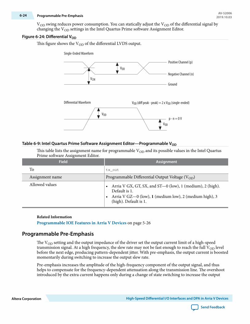
VOD swing reduces power consumption. You can statically adjust the VOD of the differential signal bychanging the VOD settings in the Intel Quartus Prime software Assignment Editor.
Figure 6-24: Differential VOD
This figure shows the VOD of the differential LVDS output.
Single-Ended Waveform
Positive Channel (p)
Negative Channel (n)
Ground
Differential Waveform
p - n = 0 V
VCM
VOD
VOD
VOD
VOD (diff peak - peak) = 2 x VOD (single-ended)
Table 6-9: Intel Quartus Prime Software Assignment Editor—Programmable VOD
This table lists the assignment name for programmable VOD and its possible values in the Intel QuartusPrime software Assignment Editor.
Field Assignment
To tx_out
Assignment name Programmable Differential Output Voltage (VOD)Allowed values • Arria V GX, GT, SX, and ST—0 (low), 1 (medium), 2 (high).
Default is 1.• Arria V GZ—0 (low), 1 (medium low), 2 (medium high), 3
(high). Default is 1.
Related InformationProgrammable IOE Features in Arria V Devices on page 5-26
Programmable Pre-EmphasisThe VOD setting and the output impedance of the driver set the output current limit of a high-speedtransmission signal. At a high frequency, the slew rate may not be fast enough to reach the full VOD levelbefore the next edge, producing pattern-dependent jitter. With pre-emphasis, the output current is boostedmomentarily during switching to increase the output slew rate.
Pre-emphasis increases the amplitude of the high-frequency component of the output signal, and thushelps to compensate for the frequency-dependent attenuation along the transmission line. The overshootintroduced by the extra current happens only during a change of state switching to increase the output
6-24 Programmable Pre-EmphasisAV-52006
2019.10.03
Altera Corporation High-Speed Differential I/O Interfaces and DPA in Arria V Devices
Send Feedback

slew rate and does not ring, unlike the overshoot caused by signal reflection. The amount of pre-emphasisrequired depends on the attenuation of the high-frequency component along the transmission line.
Figure 6-25: Programmable Pre-EmphasisThis figure shows the LVDS output with pre-emphasis.
OUT
OUT
VOD
VP
VP
Voltage boostfrom pre-emphasis
Differential outputvoltage (peak–peak)
Table 6-10: Intel Quartus Prime Software Assignment Editor—Programmable Pre-Emphasis
This table lists the assignment name for programmable pre-emphasis and its possible values in the IntelQuartus Prime software Assignment Editor.
Field Assignment
To tx_out
Assignment name Programmable Pre-emphasisAllowed values 0 (disabled), 1 (enabled). Default is 1.
Related InformationProgrammable IOE Features in Arria V Devices on page 5-26
Differential Receiver in Arria V DevicesThe receiver has a differential buffer and fractional PLLs that you can share among the transmitter andreceiver, a DPA block, a synchronizer, a data realignment block, and a deserializer. The differential buffercan receive LVDS, mini-LVDS, and RSDS signal levels. You can statically set the I/O standard of thereceiver pins to LVDS, mini-LVDS, or RSDS in the Intel Quartus Prime software Assignment Editor.
Note: To drive the LVDS channels, you must use the PLLs in integer PLL mode.
Related InformationGuideline: Use PLLs in Integer PLL Mode for LVDS on page 6-8
AV-520062019.10.03 Differential Receiver in Arria V Devices 6-25
High-Speed Differential I/O Interfaces and DPA in Arria V Devices Altera Corporation
Send Feedback

Receiver Blocks in Arria V DevicesThe Arria V differential receiver has the following hardware blocks:
• DPA block• Synchronizer• Data realignment block (bit slip)• Deserializer
The following figure shows the hardware blocks of the receiver. In SDR and DDR modes, the data widthfrom the IOE is 1 and 2 bits, respectively. The deserializer includes shift registers and parallel loadregisters, and sends a maximum of 10 bits to the internal logic.
Figure 6-26: Receiver Block Diagram
rx_in
DPA CircuitrySynchronizerBit SlipDeserializer
rx_inclock
IOE supports SDR, DDR, or non-registered datapath LVDS Receiver
FPGAFabric
rx_out
rx_divfwdclkrx_outclock
DPA Clock DomainLVDS Clock Domain
RetimedData
DPA Clock
DINDOUT DINDOUT DINDOUT DIN
Clock Mux
Fractional PLL
+–
IOE
LVDS
_diff
ioclk
DPA_
diffio
clk(LOAD_EN,diffioclk)
(DPA_LOAD_EN, DPA_diffioclk, rx_divfwdclk)
2
3
10
10
3 (LVDS_LOAD_EN,LVDS_diffioclk, rx_outclock) 8 Serial LVDS
Clock Phases
2
diffioclk
10 bitsmaximumdata width
DPA Block
The DPA block takes in high-speed serial data from the differential input buffer and selects one of theeight phases that the fractional PLLs generate to sample the data. The DPA chooses a phase closest to thephase of the serial data. The maximum phase offset between the received data and the selected phase is1/8 UI, which is the maximum quantization error of the DPA. The eight phases of the clock are equallydivided, offering a 45° resolution.
The following figure shows the possible phase relationships between the DPA clocks and the incomingserial data.
6-26 Receiver Blocks in Arria V DevicesAV-52006
2019.10.03
Altera Corporation High-Speed Differential I/O Interfaces and DPA in Arria V Devices
Send Feedback
Figure 6-27: DPA Clock Phase to Serial Data Timing Relationship
45°
90°
135°
180°
225°
270°
315°
0.125T vco
T vco
0°
rx_in D0 D1 D2 D3 D4 Dn
T VCO = PLL serial clock period
The DPA block continuously monitors the phase of the incoming serial data and selects a new clock phaseif it is required. You can prevent the DPA from selecting a new clock phase by asserting the optionalRX_DPLL_HOLD port, which is available for each channel.
DPA circuitry does not require a fixed training pattern to lock to the optimum phase out of the eightphases. After reset or power up, the DPA circuitry requires transitions on the received data to lock to theoptimum phase. An optional output port, RX_DPA_LOCKED, is available to indicate an initial DPA lockcondition to the optimum phase after power up or reset. This signal is not deasserted if the DPA selects anew phase out of the eight clock phases to sample the received data. Do not use the rx_dpa_locked signalto determine a DPA loss-of-lock condition. Use data checkers such as a cyclic redundancy check (CRC) ordiagonal interleaved parity (DIP-4) to validate the data.
An independent reset port, RX_RESET, is available to reset the DPA circuitry. You must retrain the DPAcircuitry after reset.
Note: The DPA block is bypassed in non-DPA mode.
Related InformationGuideline: Use PLLs in Integer PLL Mode for LVDS on page 6-8
Synchronizer
The synchronizer is a 1 bit wide and 6 bit deep FIFO buffer that compensates for the phase differencebetween DPA_diffioclk—the optimal clock that the DPA block selects—and the LVDS_diffioclk thatthe fractional PLLs produce. The synchronizer can only compensate for phase differences, not frequencydifferences, between the data and the receiver’s input reference clock.
An optional port, RX_FIFO_RESET, is available to the internal logic to reset the synchronizer. Thesynchronizer is automatically reset when the DPA first locks to the incoming data. Altera recommendsusing RX_FIFO_RESET to reset the synchronizer when the data checker indicates that the received data iscorrupted.
AV-520062019.10.03 Synchronizer 6-27
High-Speed Differential I/O Interfaces and DPA in Arria V Devices Altera Corporation
Send Feedback

Note: The synchronizer circuit is bypassed in non-DPA and soft-CDR mode.
Related InformationGuideline: Use PLLs in Integer PLL Mode for LVDS on page 6-8
Data Realignment Block (Bit Slip)
Skew in the transmitted data along with skew added by the link causes channel-to-channel skew on thereceived serial data streams. If you enable the DPA, the received data is captured with different clockphases on each channel. This difference may cause misalignment of the received data from channel tochannel. To compensate for this channel-to-channel skew and establish the correct received wordboundary at each channel, each receiver channel has a dedicated data realignment circuit that realigns thedata by inserting bit latencies into the serial stream.
An optional RX_CHANNEL_DATA_ALIGN port controls the bit insertion of each receiver independentlycontrolled from the internal logic. The data slips one bit on the rising edge of RX_CHANNEL_DATA_ALIGN.The requirements for the RX_CHANNEL_DATA_ALIGN signal include the following items:
• The minimum pulse width is one period of the parallel clock in the logic array.• The minimum low time between pulses is one period of the parallel clock.• The signal is an edge-triggered signal.• The valid data is available two parallel clock cycles after the rising edge of RX_CHANNEL_DATA_ALIGN.
Figure 6-28: Data Realignment Timing
This figure shows receiver output (RX_OUT) after one bit slip pulse with the deserialization factor set to 4.
rx_inclock
rx_in
rx_outclock
rx_channel_data_align
rx_out
3 2 1 0 3 2 1 0 3 2 1 0
3210 321x xx21 0321
The data realignment circuit can have up to 11 bit-times of insertion before a rollover occurs. Theprogrammable bit rollover point can be from 1 to 11 bit-times, independent of the deserialization factor.Set the programmable bit rollover point equal to, or greater than, the deserialization factor—allowingenough depth in the word alignment circuit to slip through a full word. You can set the value of the bitrollover point using the IP Catalog. An optional status port, RX_CDA_MAX, is available to the FPGA fabricfrom each channel to indicate the reaching of the preset rollover point.
6-28 Data Realignment Block (Bit Slip)AV-52006
2019.10.03
Altera Corporation High-Speed Differential I/O Interfaces and DPA in Arria V Devices
Send Feedback
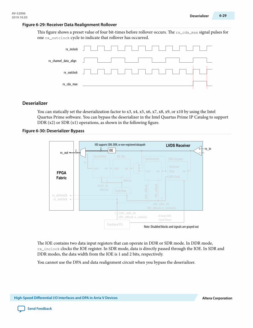
Figure 6-29: Receiver Data Realignment Rollover
This figure shows a preset value of four bit-times before rollover occurs. The rx_cda_max signal pulses forone rx_outclock cycle to indicate that rollover has occurred.
rx_inclock
rx_channel_data_align
rx_outclock
rx_cda_max
Deserializer
You can statically set the deserialization factor to x3, x4, x5, x6, x7, x8, x9, or x10 by using the IntelQuartus Prime software. You can bypass the deserializer in the Intel Quartus Prime IP Catalog to supportDDR (x2) or SDR (x1) operations, as shown in the following figure.
Figure 6-30: Deserializer Bypass
rx_in
DPA CircuitrySynchronizerBit SlipDeserializer
IOE supports SDR, DDR, or non-registered datapath LVDS Receiver
FPGAFabric
rx_out
rx_divfwdclkrx_outclock
Note: Disabled blocks and signals are grayed out
RetimedData
DPA Clock
DINDOUT DINDOUT DINDOUT DIN
Clock Mux
Fractional PLL
+–
IOELV
DS_d
iffioc
lk
DPA_
diffio
clk(LOAD_EN,diffioclk)
(DPA_LOAD_EN, DPA_diffioclk, rx_divfwdclk)
2
3
10
2
3 (LVDS_LOAD_EN,LVDS_diffioclk, rx_outclock) 8 Serial LVDS
Clock Phases
2
diffioclk
The IOE contains two data input registers that can operate in DDR or SDR mode. In DDR mode,rx_inclock clocks the IOE register. In SDR mode, data is directly passed through the IOE. In SDR andDDR modes, the data width from the IOE is 1 and 2 bits, respectively.
You cannot use the DPA and data realignment circuit when you bypass the deserializer.
AV-520062019.10.03 Deserializer 6-29
High-Speed Differential I/O Interfaces and DPA in Arria V Devices Altera Corporation
Send Feedback
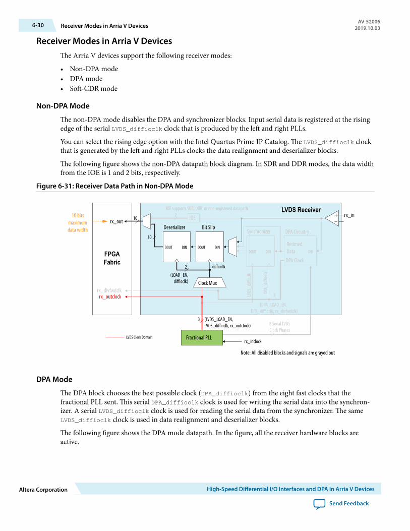
Receiver Modes in Arria V DevicesThe Arria V devices support the following receiver modes:
• Non-DPA mode• DPA mode• Soft-CDR mode
Non-DPA Mode
The non-DPA mode disables the DPA and synchronizer blocks. Input serial data is registered at the risingedge of the serial LVDS_diffioclk clock that is produced by the left and right PLLs.
You can select the rising edge option with the Intel Quartus Prime IP Catalog. The LVDS_diffioclk clockthat is generated by the left and right PLLs clocks the data realignment and deserializer blocks.
The following figure shows the non-DPA datapath block diagram. In SDR and DDR modes, the data widthfrom the IOE is 1 and 2 bits, respectively.
Figure 6-31: Receiver Data Path in Non-DPA Mode
rx_in
DPA CircuitrySynchronizerBit SlipDeserializer
rx_inclock
IOE supports SDR, DDR, or non-registered datapath LVDS Receiver
FPGAFabric
rx_out
rx_divfwdclkrx_outclock
Note: All disabled blocks and signals are grayed out
10 bitsmaximumdata width
LVDS Clock Domain
RetimedData
DPA Clock
DINDOUT DINDOUT DINDOUT DIN
Clock Mux
Fractional PLL
+–
IOE
LVDS
_diff
ioclk
DPA_
diffio
clk(LOAD_EN,diffioclk)
(DPA_LOAD_EN, DPA_diffioclk, rx_divfwdclk)
2
3
10
10
3 (LVDS_LOAD_EN,LVDS_diffioclk, rx_outclock) 8 Serial LVDS
Clock Phases
2
diffioclk
DPA Mode
The DPA block chooses the best possible clock (DPA_diffioclk) from the eight fast clocks that thefractional PLL sent. This serial DPA_diffioclk clock is used for writing the serial data into the synchron‐izer. A serial LVDS_diffioclk clock is used for reading the serial data from the synchronizer. The sameLVDS_diffioclk clock is used in data realignment and deserializer blocks.
The following figure shows the DPA mode datapath. In the figure, all the receiver hardware blocks areactive.
6-30 Receiver Modes in Arria V DevicesAV-52006
2019.10.03
Altera Corporation High-Speed Differential I/O Interfaces and DPA in Arria V Devices
Send Feedback
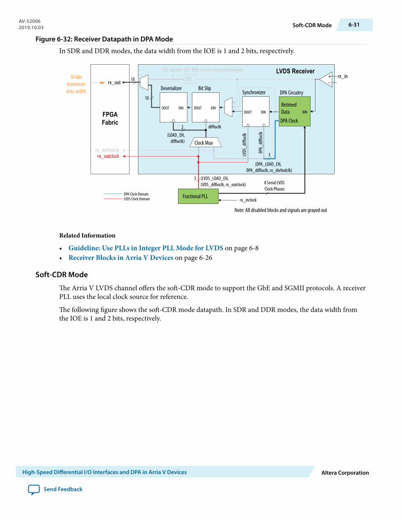
Figure 6-32: Receiver Datapath in DPA Mode
In SDR and DDR modes, the data width from the IOE is 1 and 2 bits, respectively.
rx_in
DPA CircuitrySynchronizerBit SlipDeserializer
rx_inclock
IOE supports SDR, DDR, or non-registered datapath LVDS Receiver
FPGAFabric
rx_out
rx_divfwdclkrx_outclock
Note: All disabled blocks and signals are grayed out
10 bitsmaximumdata width
DPA Clock DomainLVDS Clock Domain
RetimedData
DPA Clock
DINDOUT DINDOUT DINDOUT DIN
Clock Mux
Fractional PLL
+–
IOE
LVDS
_diff
ioclk
DPA_
diffio
clk(LOAD_EN,diffioclk)
(DPA_LOAD_EN, DPA_diffioclk, rx_divfwdclk)
2
3
10
10
3 (LVDS_LOAD_EN,LVDS_diffioclk, rx_outclock) 8 Serial LVDS
Clock Phases
2
diffioclk
Related Information
• Guideline: Use PLLs in Integer PLL Mode for LVDS on page 6-8• Receiver Blocks in Arria V Devices on page 6-26
Soft-CDR Mode
The Arria V LVDS channel offers the soft-CDR mode to support the GbE and SGMII protocols. A receiverPLL uses the local clock source for reference.
The following figure shows the soft-CDR mode datapath. In SDR and DDR modes, the data width fromthe IOE is 1 and 2 bits, respectively.
AV-520062019.10.03 Soft-CDR Mode 6-31
High-Speed Differential I/O Interfaces and DPA in Arria V Devices Altera Corporation
Send Feedback

Figure 6-33: Receiver Datapath in Soft-CDR Mode
rx_in
DPA CircuitrySynchronizerBit SlipDeserializer
rx_inclock
IOE supports SDR, DDR, or non-registered datapath LVDS Receiver
FPGAFabric
rx_out
rx_divfwdclkrx_outclock
Note: All disabled blocks and signals are grayed out
10 bitsMaximum
Data Width
DPA Clock DomainLVDS Clock Domain
RetimedData
DPA Clock
DINDOUT DINDOUT DINDOUT DIN
Clock Mux
Fractional PLL
+–
IOE
LVDS
_diff
ioclk
DPA_
diffio
clk(LOAD_EN,diffioclk)
(DPA_LOAD_EN, DPA_diffioclk, rx_divfwdclk)
2
3
10
10
3(rx_outclock) 8 Serial LVDS
Clock Phases
2
diffioclk
In soft-CDR mode, the synchronizer block is inactive. The DPA circuitry selects an optimal DPA clockphase to sample the data. Use the selected DPA clock for bit-slip operation and deserialization. The DPAblock also forwards the selected DPA clock, divided by the deserialization factor called rx_divfwdclk, tothe FPGA fabric, along with the deserialized data. This clock signal is put on the periphery clock (PCLK)network.
If you use the soft-CDR mode, do not assert the rx_reset port after the DPA has trained. The DPAcontinuously chooses new phase taps from the PLL to track parts per million (PPM) differences betweenthe reference clock and incoming data.
You can use every LVDS channel in soft-CDR mode and drive the FPGA fabric using the PCLK networkin the Arria V device family. The rx_dpa_locked signal is not valid in soft-CDR mode because the DPAcontinuously changes its phase to track PPM differences between the upstream transmitter and the localreceiver input reference clocks. The parallel clock, rx_outclock, generated by the left and right PLLs, isalso forwarded to the FPGA fabric.
Related InformationPeriphery Clock Networks on page 4-5Provides more information about PCLK networks.
Receiver Clocking for Arria V DevicesThe fractional PLL receives the external clock input and generates different phases of the same clock. TheDPA block automatically chooses one of the clocks from the fractional PLL and aligns the incoming dataon each channel.
The synchronizer circuit is a 1 bit wide by 6 bit deep FIFO buffer that compensates for any phasedifference between the DPA clock and the data realignment block. If necessary, the user-controlled datarealignment circuitry inserts a single bit of latency in the serial bit stream to align to the word boundary.
6-32 Receiver Clocking for Arria V DevicesAV-52006
2019.10.03
Altera Corporation High-Speed Differential I/O Interfaces and DPA in Arria V Devices
Send Feedback
The physical medium connecting the transmitter and receiver LVDS channels may introduce skewbetween the serial data and the source-synchronous clock. The instantaneous skew between each LVDSchannel and the clock also varies with the jitter on the data and clock signals as seen by the receiver. Thethree different modes—non-DPA, DPA, and soft-CDR—provide different options to overcome skewbetween the source synchronous clock (non-DPA, DPA) /reference clock (soft-CDR) and the serial data.
Non-DPA mode allows you to statically select the optimal phase between the source synchronous clockand the received serial data to compensate skew. In DPA mode, the DPA circuitry automatically choosesthe best phase to compensate for the skew between the source synchronous clock and the received serialdata. Soft-CDR mode provides opportunities for synchronous and asynchronous applications for chip-to-chip and short reach board-to-board applications for SGMII protocols.
Note: Only the non-DPA mode requires manual skew adjustment.
Related InformationGuideline: Use PLLs in Integer PLL Mode for LVDS on page 6-8
Differential I/O Termination for Arria V Devices
The Arria V devices provide a 100 Ω, on-chip differential termination option on each differential receiverchannel for LVDS standards. On-chip termination saves board space by eliminating the need to addexternal resistors on the board. You can enable on-chip termination in the Intel Quartus Prime softwareAssignment Editor.
All I/O pins and dedicated clock input pins support on-chip differential termination, RD OCT.
Figure 6-34: On-Chip Differential I/O Termination
Differential Receiverwith On-Chip 100 Ω
TerminationLVDS
TransmitterZ 0 = 50 Ω
Z 0 = 50 Ω
R D
Table 6-11: Intel Quartus Prime Software Assignment Editor—On-Chip Differential Termination
This table lists the assignment name for on-chip differential termination in the Intel Quartus Primesoftware Assignment Editor.
Field Assignment
To rx_in
Assignment name Input Termination
Value Differential
AV-520062019.10.03 Differential I/O Termination for Arria V Devices 6-33
High-Speed Differential I/O Interfaces and DPA in Arria V Devices Altera Corporation
Send Feedback

Source-Synchronous Timing BudgetThe topics in this section describe the timing budget, waveforms, and specifications for source-synchro‐nous signaling in the Arria V device family.
The LVDS I/O standard enables high-speed transmission of data, resulting in better overall systemperformance. To take advantage of fast system performance, you must analyze the timing for these high-speed signals. Timing analysis for the differential block is different from traditional synchronous timinganalysis techniques.
The basis of the source synchronous timing analysis is the skew between the data and the clock signalsinstead of the clock-to-output setup times. High-speed differential data transmission requires the use oftiming parameters provided by IC vendors and is strongly influenced by board skew, cable skew, and clockjitter.
This section defines the source-synchronous differential data orientation timing parameters, the timingbudget definitions for the Arria V device family, and how to use these timing parameters to determine themaximum performance of a design.
Differential Data OrientationThere is a set relationship between an external clock and the incoming data. For operations at 1 Gbps anda serialization factor of 10, the external clock is multiplied by 10. You can set phase-alignment in the PLLto coincide with the sampling window of each data bit. The data is sampled on the falling edge of themultiplied clock.
Figure 6-35: Bit Orientation in the Intel Quartus Prime Software
This figure shows the data bit orientation of the x10 mode.
9 8 7 6 5 4 3 2 1 0
10 LVDS BitsMSB LSB
incloc k/outcloc k
data in
Differential I/O Bit PositionData synchronization is necessary for successful data transmission at high frequencies.
The following figure shows the data bit orientation for a channel operation and is based on the followingconditions:
• The serialization factor is equal to the clock multiplication factor.• The phase alignment uses edge alignment.• The operation is implemented in hard SERDES.
6-34 Source-Synchronous Timing BudgetAV-52006
2019.10.03
Altera Corporation High-Speed Differential I/O Interfaces and DPA in Arria V Devices
Send Feedback

Figure 6-36: Bit-Order and Word Boundary for One Differential Channel
7 6 5 4 3 2 1 0MSB LSB
X X X X X X X X X X X X X X X XCurrent Cycle
XX X X X X X X Xrx_in 7 6 5 4 3 2 1 0 X X X X X X X X X X X X X X X
rx_out [7..0] X X X X X X X X X X X X X X X X X X X X 7 6 5 4 3 2 1 0 X X X X
Previous Cycle Next Cycletx_out
tx_outclock
rx_inclock
rx_outclock
Transmitter Channel Operation (x8 Mode)
Receiver Channel Operation (x8 Mode)
Note: These waveforms are only functional waveforms and do not convey timing information
For other serialization factors, use the Intel Quartus Prime software tools to find the bit position within theword.
Differential Bit Naming Conventions
The following table lists the conventions for differential bit naming for 18 differential channels. The MSBand LSB positions increase with the number of channels used in a system.
Table 6-12: Differential Bit Naming
This table lists the conventions for differential bit naming for 18 differential channels. The MSB and LSBpositions increase with the number of channels used in a system.
Receiver Channel Data NumberInternal 8-Bit Parallel Data
MSB Position LSB Position
1 7 02 15 83 23 164 31 245 39 326 47 407 55 488 63 569 71 64
10 79 7211 87 8012 95 8813 103 96
AV-520062019.10.03 Differential Bit Naming Conventions 6-35
High-Speed Differential I/O Interfaces and DPA in Arria V Devices Altera Corporation
Send Feedback

Receiver Channel Data NumberInternal 8-Bit Parallel Data
MSB Position LSB Position
14 111 10415 119 11216 127 12017 135 12818 143 136
Transmitter Channel-to-Channel SkewThe receiver skew margin calculation uses the transmitter channel-to-channel skew (TCCS)—animportant parameter based on the Arria V transmitter in a source-synchronous differential interface:
• TCCS is the difference between the fastest and slowest data output transitions, including the TCOvariation and clock skew.
• For LVDS transmitters, the Timing Analyzer provides the TCCS value in the TCCS report(report_TCCS) in the Intel Quartus Prime compilation report, which shows TCCS values for serialoutput ports.
• You can also get the TCCS value from the device datasheet.
Note: For the Arria V GZ devices, perform PCB trace compensation to adjust the trace length of eachLVDS channel to improve channel-to-channel skew when interfacing with non-DPA receivers atdata rate above 840 Mbps.
The Intel Quartus Prime software Fitter Report panel reports the amount of delay you must add to eachtrace for the Arria V device. You can use the recommended trace delay numbers published under theLVDS Transmitter/Receiver Package Skew Compensation panel and manually compensate the skew on thePCB board trace to reduce channel-to-channel skew, thus meeting the timing budget between LVDSchannels.
Related Information
• Arria V GX, GT, XS, and ST Device Datasheet• Arria V GZ Device Datasheet• LVDS SERDES Transmitter/Receiver IP Cores User Guide
More information about the LVDS Transmitter/Receiver Package Skew Compensation report panel.
Receiver Skew Margin for Non-DPA ModeDifferent modes of LVDS receivers use different specifications, which can help in deciding the ability tosample the received serial data correctly:
• In DPA mode, use DPA jitter tolerance instead of the receiver skew margin (RSKM).• In non-DPA mode, use RSKM, TCCS, and sampling window (SW) specifications for high-speed
source-synchronous differential signals in the receiver data path.
The following equation expresses the relationship between RSKM, TCCS, and SW.
6-36 Transmitter Channel-to-Channel SkewAV-52006
2019.10.03
Altera Corporation High-Speed Differential I/O Interfaces and DPA in Arria V Devices
Send Feedback
Figure 6-37: RSKM Equation
Conventions used for the equation:
• RSKM—the timing margin between the receiver’s clock input and the data input sampling window.• Time unit interval (TUI)—time period of the serial data.• SW—the period of time that the input data must be stable to ensure that data is successfully sampled by
the LVDS receiver. The SW is a device property and varies with device speed grade.• TCCS—the timing difference between the fastest and the slowest output edges, including tCO variation
and clock skew, across channels driven by the same PLL. The clock is included in the TCCS measure‐ment.
You must calculate the RSKM value to decide whether the LVDS receiver can sample the data properly ornot, given the data rate and device. A positive RSKM value indicates that the LVDS receiver can samplethe data properly, whereas a negative RSKM indicates that it cannot sample the data properly.
The following figure shows the relationship between the RSKM, TCCS, and the SW of the receiver.
AV-520062019.10.03 Receiver Skew Margin for Non-DPA Mode 6-37
High-Speed Differential I/O Interfaces and DPA in Arria V Devices Altera Corporation
Send Feedback

Figure 6-38: Differential High-Speed Timing Diagram and Timing Budget for Non-DPA Mode
TUI
Time Unit Interval (TUI)
TCCS
InternalClock
Falling Edge
tSW (min)Bit n
tSW (max)Bit n
TCCSTCCS
2
ReceiverInput Data
TransmitterOutput Data
InternalClockSynchronization
ExternalClock
ReceiverInput Data
InternalClock
ExternalInput Clock
Timing Budget
Timing Diagram
Clock Placement
SW
TCCS
RSKM RSKM
SW
RSKM RSKM
For LVDS receivers, the Intel Quartus Prime software provides an RSKM report showing the SW, TUI, andRSKM values for non-DPA LVDS mode:
• You can generate the RSKM report by executing the report_RSKM command in the TimingAnalyzer. You can find the RSKM report in the Intel Quartus Prime compilation report in the TimingAnalyzer section.
• To obtain the RSKM value, assign the input delay to the LVDS receiver through the constraints menu ofthe Timing Analyzer. The input delay is determined according to the data arrival time at the LVDSreceiver port, with respect to the reference clock.
• If you set the input delay in the settings parameters for the Set Input Delay option, set the clock nameto the clock that reference the source synchronous clock that feeds the LVDS receiver.
• If you do not set any input delay in the Timing Analyzer, the receiver channel-to-channel skew defaultsto zero.
• You can also directly set the input delay in a Synopsys Design Constraint file (.sdc) using theset_input_delay command.
6-38 Receiver Skew Margin for Non-DPA ModeAV-52006
2019.10.03
Altera Corporation High-Speed Differential I/O Interfaces and DPA in Arria V Devices
Send Feedback
Related Information
• LVDS SERDES Transmitter/Receiver IP Cores User GuideMore information about the RSKM equation and calculation.
• The Intel Quartus Prime Timing Analyzer chapter, Intel Quartus Prime Standard EditionHandbook Volume 3 VerificationProvides more information about .sdc commands and the Timing Analyzer.
Assigning Input Delay to LVDS Receiver Using Timing Analyzer
To obtain the RSKM value, assign an appropriate input delay to the LVDS receiver from the TimingAnalyzer constraints menu.
1. On the menu in the Timing Analyzer, select Constraints > Set Input Delay.2. In the Set Input Delay window, select the desired clock using the pull-down menu. The clock name
must reference the source synchronous clock that feeds the LVDS receiver.3. Click the Browse button (next to the Targets field).4. In the Name Finder window, click List to view a list of all available ports. Select the LVDS receiver
serial input ports according to the input delay you set, and click OK.5. In the Set Input Delay window, set the appropriate values in the Input delay options and Delay value
fields.6. Click Run to incorporate these values in the Timing Analyzer.7. Repeat from step 1 to assign the appropriate delay for all the LVDS receiver input ports. If you have
already assigned Input Delay and you need to add more delay to that input port, turn on the AddDelay option.
High-Speed Differential I/O Interfaces and DPA in Arria V DevicesRevision History
Date Version Changes
December2017
2017.12.15 • Added a note to Guideline: Use High-Speed Clock from PLL to ClockLVDS SERDES Only topic to clarify that spread-spectrum input clockis not supported in LVDS.
• Updated for latest Intel branding standards.
December2015
2015.12.21 Changed instances of Quartus II to Quartus Prime.
AV-520062019.10.03 Assigning Input Delay to LVDS Receiver Using Timing Analyzer 6-39
High-Speed Differential I/O Interfaces and DPA in Arria V Devices Altera Corporation
Send Feedback
Date Version Changes
May 2015 2015.05.08 • Changed figure title "Corner PLLs Driving DPA-enabled DifferentialI/Os" to "Invalid Usage of Corner PLLs Driving DPA-enabledDifferential I/Os".
• Added LVDS and DPA Clock Network figure in Guideline: UsingDPA-Enabled Differential Channels.
• Updated all figures in Guideline: Using DPA-Enabled DifferentialChannels.
• Updated guidelines for using both corner PLLs in Arria V Devices.• Updated figures in Guideline: Using DPA-Disabled LVDS Differential
Channels.• Updated the statement about emulated LVDS buffers to specify that
you can use true LVDS input buffer as emulated output buffers forserialization factor of 1 and 2.
January 2015 2015.01.19 • Removed statement on explanation related to rx_synclock for figure"LVDS Interface with the Altera_PLL Megafunction (With Soft-CDRMode)".
• Updated figure LVDS Interface with the Altera_PLL Megafunction(With Soft-CDR Mode) and figure Receiver Datapath in Soft-CDRMode.
• Added a note to leave rx_enable and rx_inclock to be unconnected forfigure LVDS Interface with the Altera_PLL Megafunction (With Soft-CDR Mode).
• Updated timing diagram for Phase Relationship for External PLLInterface Signals to reflect the correct phase shift and frequency foroutclk2.
January 2014 2014.01.10 • Updated the statement about setting the phase of the clock in relationto data in the topic about transmitter clocking.
• Added a figure that shows the phase relationship for the external PLLinterface signals.
• Clarified that "one row of separation" between two groups of DPA-enabled channels means a separation of one differential channel.
• Clarified that "internal PLL option" refers to the option in theALTLVDS megafunction.
• Updated the topic about emulated LVDS buffers to clarify that youcan use unutilized true LVDS input channels (instead "buffers") asemulated LVDS output buffers.
August 2013 2013.08.19 Updated the number of LVDS channels of the Arria V GZ E5 and E7devices (1517-pin package) from 80 to 79 (top banks TX) and 82 to 81(top banks RX).
June 2013 2013.06.21 Updated the figure about data realignment timing to correct the datapattern after a bit slip.
6-40 High-Speed Differential I/O Interfaces and DPA in Arria V Devices Revision HistoryAV-52006
2019.10.03
Altera Corporation High-Speed Differential I/O Interfaces and DPA in Arria V Devices
Send Feedback

Date Version Changes
May 2013 2013.05.06 • Moved all links to the Related Information section of respective topicsfor easy reference.
• Added link to the known document issues in the Knowledge Base.• Clarified that the clock tree network cannot cross over to different I/O
regions only applies to Arria V GZ.• Added a figure to show the center PLLs driving the DPA-enabled
differential I/Os in Arria V GZ devices.• Changed the color of the transceiver blocks in the high-speed
differential I/O location diagrams for clarity.• Reorganized contents under the differential receiver topic.• Added a topic about emulated LVDS buffers.• Edited the topic about true LVDS buffers.• Corrected references to upper and lower I/O banks to left and right I/
O banks, respectively.• Updated the data realignment timing figure to improve clarity.• Updated the receiver data realignment rollover figure to improve
clarity.
November2012
2012.11.19 • Reorganized content and updated template.• Added Arria V GZ information.• Added Altera_PLL settings for external PLL usage in DPA and non-
DPA modes.• Updated clocking examples. Altera_PLL now supports entering
negative phase shift.• Rearranged the LVDS channel counts table into several tables
according to device variant for ease of reference.• Updated the Arria V GX A1 and A3 LVDS channel counts, and added
the channel counts for Arria V GZ.• Removed references to ALTPLL and added information about Altera_
PLL. Altera_PLL now replaces ALTPLL for Arria V devices.• Added design guidelines for using LVDS interface with the external
PLL mode. These include information on the signal interfaces, theparameter values, and the connection between Altera_PLL andALTLVDS in external PLL mode.
• Updated the programmable VOD allowed values for Arria V GX, GT,SX, and ST, and added the values for Arria V GZ.
• Moved the PLL and clocking section into design guideline topics.• Added steps to assign input delay to LVDS receiver using the
TimeQuest Timing Analyzer.
AV-520062019.10.03 High-Speed Differential I/O Interfaces and DPA in Arria V Devices Revision History 6-41
High-Speed Differential I/O Interfaces and DPA in Arria V Devices Altera Corporation
Send Feedback
Date Version Changes
June 2012 2.0 • Restructured the chapter.• Updated Table 6–1.• Updated Figure 6–1 and Figure 6–2.• Added Figure 6–3.• Added “Design Considerations” section.• Updated the “Differential Pin Placement” section.
November2011
1.1 • Updated Table 6–1.• Restructured chapter.
May 2011 1.0 Initial release.
6-42 High-Speed Differential I/O Interfaces and DPA in Arria V Devices Revision HistoryAV-52006
2019.10.03
Altera Corporation High-Speed Differential I/O Interfaces and DPA in Arria V Devices
Send Feedback
External Memory Interfaces in Arria V Devices 72019.10.03
AV-52007 Subscribe Send Feedback
The Arria V devices provide an efficient architecture that allows you to fit wide external memory interfacesto support a high level of system bandwidth within the small modular I/O bank structure. The I/Os aredesigned to provide high-performance support for existing and emerging external memory standards.
Table 7-1: Supported External Memory Standards in Arria V Devices
Memory Standard
Hard MemoryController
Soft Memory Controller
Arria V GX, GT, SX, andST
Arria V GX, GT, SX, andST
Arria V GZ
DDR3 SDRAM Full rate Half rate and quarterrate
Half rate and quarter rate
DDR2 SDRAM Full rate Half rate Full rate and half rate
LPDDR2 SDRAM — Half rate —
RLDRAM 3 — — Half rate and quarter rate
RLDRAM II — Half rate Full rate and half rate
QDR II+ SRAM — Half rate Full rate and half rate
QDR II SRAM — Half rate Full rate and half rate
Related Information
• Arria V Device Handbook: Known IssuesLists the planned updates to the Arria V Device Handbook chapters.
• External Memory Interface Spec EstimatorFor the latest information and to estimate the external memory system performance specification, useAltera's External Memory Interface Spec Estimator tool.
• External Memory Interfaces Handbook Volume 1, 2, and 3.Provides more information about the memory types supported, board design guidelines, timinganalysis, simulation, and debugging information.
Intel Corporation. All rights reserved. Intel, the Intel logo, Altera, Arria, Cyclone, Enpirion, MAX, Nios, Quartus and Stratix words and logos are trademarks ofIntel Corporation or its subsidiaries in the U.S. and/or other countries. Intel warrants performance of its FPGA and semiconductor products to currentspecifications in accordance with Intel's standard warranty, but reserves the right to make changes to any products and services at any time without notice.Intel assumes no responsibility or liability arising out of the application or use of any information, product, or service described herein except as expresslyagreed to in writing by Intel. Intel customers are advised to obtain the latest version of device specifications before relying on any published informationand before placing orders for products or services.*Other names and brands may be claimed as the property of others.
ISO9001:2015Registered
www.altera.com101 Innovation Drive, San Jose, CA 95134

External Memory Performance
Table 7-2: External Memory Interface Performance in Arria V Devices
Interface Voltage(V)
Hard Controller(MHz)
Soft Controller (MHz)
Arria V GX, GT, SX,and ST
Arria V GX, GT, SX,and ST
Arria V GZ
DDR3 SDRAM1.5 533 667 800
1.35 533 600 800DDR2 SDRAM 1.8 400 400 400LPDDR2SDRAM
1.2 — 400 —
RLDRAM 3 1.2 — — 667
RLDRAM II1.8 — 400 5331.5 — 400 533
QDR II+ SRAM1.8 — 400 5001.5 — 400 500
QDR II SRAM1.8 — 400 3331.5 — 400 333
DDR II+SRAM(23)
1.8 — 400 —1.5 — 400 —
Related InformationExternal Memory Interface Spec EstimatorFor the latest information and to estimate the external memory system performance specification, useAltera's External Memory Interface Spec Estimator tool.
HPS External Memory Performance
Table 7-3: HPS External Memory Interface Performance
The hard processor system (HPS) is available in Arria V SoC devices only.Interface Voltage (V) HPS Hard Controller (MHz)
DDR3 SDRAM1.5 533
1.35 533LPDDR2 SDRAM 1.2 333
(23) Not available as Intel IP.
7-2 External Memory PerformanceAV-52007
2019.10.03
Altera Corporation External Memory Interfaces in Arria V Devices
Send Feedback
Related InformationExternal Memory Interface Spec EstimatorFor the latest information and to estimate the external memory system performance specification, useAltera's External Memory Interface Spec Estimator tool.
Memory Interface Pin Support in Arria V DevicesIn the Arria V devices, the memory interface circuitry is available in every I/O bank that does not supporttransceivers. The devices offer differential input buffers for differential read-data strobe and clockoperations.
The memory clock pins are generated with double data rate input/output (DDRIO) registers.
Related InformationPlanning Pin and FPGA Resources chapter, External Memory Interface HandbookProvides more information about which pins to use for memory clock pins and pin location requirements.
Guideline: Using DQ/DQS PinsThe following list provides guidelines on using the DQ/DQS pins:
• The devices support DQ and DQS signals with DQ bus modes of x4/x8/x9, x16/x18, or x32/x36.• You can use the DQSn or CQn pins that are not used for clocking as DQ pins.• If you do not use the DQ/DQS pins for memory interfacing, you can use these pins as user I/Os.
However, unused HPS DQ/DQS pins on the Arria V SX and ST devices cannot be used as user I/Os.• Some pins have multiple functions such as RZQ or DQ. If you need extra RZQ pins, you can use some
of the DQ pins as RZQ pins instead.
Note: For the x8, x16/x18, or x32/x36 DQ/DQS groups whose members are used as RZQ pins, Alterarecommends that you assign the DQ and DQS pins manually. Otherwise, the Intel Quartus Primesoftware might not be able to place the DQ and DQS pins, resulting in a “no-fit” error.
Reading the Pin Table
For the maximum number of DQ pins and the exact number per group for a particular Arria V device,refer to the relevant device pin table.
In the pin tables, the DQS and DQSn pins denote the differential data strobe/clock pin pairs, while the CQand CQn pins denote the complementary echo clock signals. The pin table lists the parity, DM, BWSn,NWSn, ECC, and QVLD pins as DQ pins.
Related Information
• Planning Pin and FPGA Resources chapter, External Memory Interface HandbookProvides more information about read clock pins usage for QDR II and QDR II+ SRAM, andRLDRAM II interfaces in Arria V GX, GT, SX, and ST devices
• Arria V Device Pin-Out FilesDownload the relevant pin tables from this web page.
AV-520072019.10.03 Memory Interface Pin Support in Arria V Devices 7-3
External Memory Interfaces in Arria V Devices Altera Corporation
Send Feedback

DQ/DQS Bus Mode Pins for Arria V DevicesThe following tables list the pin support per DQ/DQS bus mode, including the DQS/CQ/CQn/QK# andDQSn pins. The maximum number of data pins per group listed in the tables may vary according to thefollowing conditions:
• Single-ended DQS signaling—the maximum number of DQ pins includes parity, data mask, andQVLD pins connected to the DQS bus network.
• Differential or complementary DQS signaling—the maximum number of data pins per group decreasesby one. This number may vary per DQ/DQS group in a particular device. Check the pin table for theexact number per group.
• DDR3 and DDR2 interfaces—the maximum number of pins is further reduced for an interface largerthan x8 because you require one DQS pin for each x8/x9 group to form the x16/x18 and x32/x36groups.
Table 7-4: DQ/DQS Bus Mode Pins for Arria V GX, GT, SX, and ST Devices
ModeDQSn
SupportCQn
Support
Parity orDataMask
(Optional)
QVLD (24)
(Optional)
Data Pins perGroup
NotesTypicalMaximu
m
x4/x8/x9 Yes Yes Yes Yes 4, 8, or 9 11 The x4 mode uses x8/x9 groups.
x16/x18 Yes Yes Yes Yes 16 or 18 23 Two x8 DQ/DQS groups are stitchedto create a x16/x18 group, so thereare 24 pins in this group.
x32/x36 Yes Yes Yes Yes 32 or 36 47 Four x8 DQ/DQS groups arestitched to create a x32/x36 group,so there are 48 pins in this group.
Table 7-5: DQ/DQS Bus Mode Pins for Arria V GZ Devices
ModeDQSn
SupportCQn
Support
Parity orDataMask
(Optional)
QVLD (24)
(Optional)
Data Pins perGroup
NotesTypicalMaximu
m
x4 Yes — — — 4 5 If you do not use differential DQSand the group does not haveadditional signals, the data mask(DM) pin is supported.
x8/x9 Yes Yes Yes Yes 8 or 9 11 Two x4 DQ/DQS groups are stitchedto create a x8/x9 group, so there area total of 12 pins in this group.
(24) The QVLD pin is not used in the UniPHY IP core.
7-4 DQ/DQS Bus Mode Pins for Arria V DevicesAV-52007
2019.10.03
Altera Corporation External Memory Interfaces in Arria V Devices
Send Feedback

ModeDQSn
SupportCQn
Support
Parity orDataMask
(Optional)
QVLD (24)
(Optional)
Data Pins perGroup
NotesTypicalMaximu
m
x16/x18 Yes Yes Yes Yes 16 or 18 23 Four x4 DQ/DQS groups arestitched to create a x16/x18 group;so there are a total of 24 pins in thisgroup.
x32/x36 Yes Yes Yes Yes 32 or 36 47 Eight x4 DQ/DQS groups arestitched to create a x32/x36 group,so there are a total of 48 pins in thisgroup.
DQ/DQS Groups in Arria V GX
Table 7-6: Number of DQ/DQS Groups Per Side in Arria V GX Devices
This table lists the DQ/DQS groups for the soft memory controller. For the hard memory controller, youcan get the DQ/DQS groups from the pin table of the specific device.
MemberCode Package Side x8/x9 x16/x18 x32/x36
A1
672-pin FineLine BGA, Flip ChipTop 8 3 —
Bottom 8 3 —Right 4 2 —
896-pin FineLine BGA, Flip ChipTop 10 3 —
Bottom 10 3 —Right 6 2 —
A3
672-pin FineLine BGA, Flip ChipTop 8 3 —
Bottom 8 3 —Right 4 2 —
896-pin FineLine BGA, Flip ChipTop 10 3 —
Bottom 10 3 —Right 6 2 —
A5
672-pin FineLine BGA, Flip ChipTop 8 3 1
Bottom 8 3 1
896-pin FineLine BGA, Flip ChipTop 12 5 1
Bottom 12 5 1
1152-pin FineLine BGA, Flip ChipTop 17 8 2
Bottom 17 8 2
AV-520072019.10.03 DQ/DQS Groups in Arria V GX 7-5
External Memory Interfaces in Arria V Devices Altera Corporation
Send Feedback
MemberCode Package Side x8/x9 x16/x18 x32/x36
A7
672-pin FineLine BGA, Flip ChipTop 8 3 1
Bottom 8 3 1
896-pin FineLine BGA, Flip ChipTop 12 5 1
Bottom 12 5 1
1152-pin FineLine BGA, Flip ChipTop 17 8 2
Bottom 17 8 2
B1
896-pin FineLine BGA, Flip ChipTop 12 5 1
Bottom 12 5 1
1517-pin FineLine BGA, Flip ChipTop 22 10 4
Bottom 22 10 4
1152-pin FineLine BGA, Flip ChipTop 17 8 2
Bottom 17 8 2
B3
896-pin FineLine BGA, Flip ChipTop 12 5 1
Bottom 12 5 1
1152-pin FineLine BGA, Flip ChipTop 17 8 2
Bottom 17 8 2
1517-pin FineLine BGA, Flip ChipTop 22 10 4
Bottom 22 10 4
B51152-pin FineLine BGA, Flip Chip
Top 17 8 2Bottom 17 8 2
1517-pin FineLine BGA, Flip ChipTop 22 10 4
Bottom 22 10 4
B71152-pin FineLine BGA, Flip Chip
Top 17 8 2Bottom 17 8 2
1517-pin FineLine BGA, Flip ChipTop 22 10 4
Bottom 22 10 4
Related InformationArria V Device Pin-Out FilesDownload the relevant pin tables from this web page.
7-6 DQ/DQS Groups in Arria V GXAV-52007
2019.10.03
Altera Corporation External Memory Interfaces in Arria V Devices
Send Feedback

DQ/DQS Groups in Arria V GT
Table 7-7: Number of DQ/DQS Groups Per Side in Arria V GT Devices
This table lists the DQ/DQS groups for the soft memory controller. For the hard memory controller, youcan get the DQ/DQS groups from the pin table of the specific device.
MemberCode Package Side x8/x9 x16/x18 x32/x36
C3
672-pin FineLine BGA, Flip ChipTop 8 3 —
Bottom 8 3 —Right 4 2 —
896-pin FineLine BGA, Flip ChipTop 10 3 —
Bottom 10 3 —Right 6 2 —
C7896-pin FineLine BGA, Flip Chip
Top 12 5 1Bottom 12 5 1
1152-pin FineLine BGA, Flip ChipTop 17 8 2
Bottom 17 8 2
D3
896-pin FineLine BGA, Flip ChipTop 12 5 1
Bottom 12 5 1
1152-pin FineLine BGA, Flip ChipTop 17 8 2
Bottom 17 8 2
1517-pin FineLine BGA, Flip ChipTop 22 10 4
Bottom 22 10 4
D71152-pin FineLine BGA, Flip Chip
Top 17 8 2Bottom 17 8 2
1517-pin FineLine BGA, Flip ChipTop 22 10 4
Bottom 22 10 4
Related InformationArria V Device Pin-Out FilesDownload the relevant pin tables from this web page.
AV-520072019.10.03 DQ/DQS Groups in Arria V GT 7-7
External Memory Interfaces in Arria V Devices Altera Corporation
Send Feedback

DQ/DQS Groups in Arria V GZ
Table 7-8: Number of DQ/DQS Groups Per Side in Arria V GZ Devices
MemberCode Package Side x4 x8/x9 x16/x18 x32/x36
E1780-pin FineLine BGA, Flip Chip
Top 28 13 6 2Bottom 26 13 6 1
1152-pin FineLine BGA, Flip ChipTop 32 15 7 2
Bottom 34 17 8 2
E3780-pin FineLine BGA, Flip Chip
Top 28 13 6 2Bottom 26 13 6 1
1152-pin FineLine BGA, Flip ChipTop 32 15 7 2
Bottom 34 17 8 2
E51152-pin FineLine BGA, Flip Chip
Top 36 17 8 3Bottom 50 25 12 4
1517-pin FineLine BGA, Flip ChipTop 52 26 12 6
Bottom 58 29 14 6
E71152-pin FineLine BGA, Flip Chip
Top 36 17 8 3Bottom 50 25 12 4
1517-pin FineLine BGA, Flip ChipTop 52 26 12 6
Bottom 58 29 14 6
DQ/DQS Groups in Arria V SX
Table 7-9: Number of DQ/DQS Groups Per Side in Arria V SX Devices
This table lists the DQ/DQS groups for the soft memory controller. For the hard memory controller, youcan get the DQ/DQS groups from the pin table of the specific device.
MemberCode Package Side x8/x9 x16/x18 x32/x36
B3
896-pin FineLine BGA, Flip ChipTop 7 3 1
Bottom 6 2 —
1152-pin FineLine BGA, Flip ChipTop 7 3 1
Bottom 16 7 2
1517-pin FineLine BGA, Flip ChipTop 11 5 2
Bottom 22 10 4
7-8 DQ/DQS Groups in Arria V GZAV-52007
2019.10.03
Altera Corporation External Memory Interfaces in Arria V Devices
Send Feedback
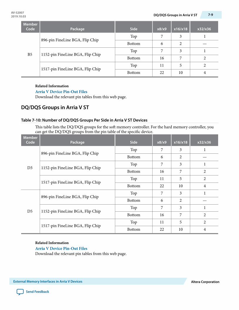
MemberCode Package Side x8/x9 x16/x18 x32/x36
B5
896-pin FineLine BGA, Flip ChipTop 7 3 1
Bottom 6 2 —
1152-pin FineLine BGA, Flip ChipTop 7 3 1
Bottom 16 7 2
1517-pin FineLine BGA, Flip ChipTop 11 5 2
Bottom 22 10 4
Related InformationArria V Device Pin-Out FilesDownload the relevant pin tables from this web page.
DQ/DQS Groups in Arria V ST
Table 7-10: Number of DQ/DQS Groups Per Side in Arria V ST Devices
This table lists the DQ/DQS groups for the soft memory controller. For the hard memory controller, youcan get the DQ/DQS groups from the pin table of the specific device.
MemberCode Package Side x8/x9 x16/x18 x32/x36
D3
896-pin FineLine BGA, Flip ChipTop 7 3 1
Bottom 6 2 —
1152-pin FineLine BGA, Flip ChipTop 7 3 1
Bottom 16 7 2
1517-pin FineLine BGA, Flip ChipTop 11 5 2
Bottom 22 10 4
D5
896-pin FineLine BGA, Flip ChipTop 7 3 1
Bottom 6 2 —
1152-pin FineLine BGA, Flip ChipTop 7 3 1
Bottom 16 7 2
1517-pin FineLine BGA, Flip ChipTop 11 5 2
Bottom 22 10 4
Related InformationArria V Device Pin-Out FilesDownload the relevant pin tables from this web page.
AV-520072019.10.03 DQ/DQS Groups in Arria V ST 7-9
External Memory Interfaces in Arria V Devices Altera Corporation
Send Feedback

External Memory Interface Features in Arria V DevicesThe Arria V I/O elements (IOE) provide built-in functionality required for a rapid and robust implemen‐tation of external memory interfacing.
The following device features are available for external memory interfaces:
• DQS phase-shift circuitry• PHY Clock (PHYCLK) networks• DQS logic block• Dynamic on-chip termination (OCT) control• IOE registers• Delay chains• Hard memory controllers (Arria V GX, GT, SX, and ST only)• Read- and write-leveling support (Arria V GZ only)
UniPHY IPThe high-performance memory interface solution includes the self-calibrating UniPHY IP that isoptimized to take advantage of the Arria V I/O structure and the Intel Quartus Prime software TimingAnalyzer. The UniPHY IP helps set up the physical interface (PHY) best suited for your system. Thisprovides the total solution for the highest reliable frequency of operation across process, voltage, andtemperature (PVT) variations.
The UniPHY IP instantiates a PLL to generate related clocks for the memory interface. The UniPHY IPcan also dynamically choose the number of delay chains that are required for the system. The amount ofdelay is equal to the sum of the intrinsic delay of the delay element and the product of the number of delaysteps and the value of the delay steps.
The UniPHY IP and the Altera memory controller IP core can run at half the I/O interface frequency ofthe memory devices, allowing better timing management in high-speed memory interfaces. The Arria Vdevices contain built-in circuitry in the IOE to convert data from full rate (the I/O frequency) to half rate(the controller frequency) and vice versa.
Related InformationFunctional Description - UniPHY, External Memory Interface Handbook Volume 3Provides more information about UniPHY IP.
External Memory Interface DatapathThe following figures show overviews of the memory interface datapath that uses the Arria V I/Oelements. In the figures, the DQ/DQS read and write signals may be bidirectional or unidirectional,depending on the memory standard. If the signal is bidirectional, it is active during read and writeoperations.
7-10 External Memory Interface Features in Arria V DevicesAV-52007
2019.10.03
Altera Corporation External Memory Interfaces in Arria V Devices
Send Feedback

Figure 7-1: External Memory Interface Datapath Overview for Arria V GX, GT, SX, and ST Devices
MemoryFPGA
DLL
4nn
n
2n
DQ (Read)
DQ (Write)
Read FIFO
DQS (Read)
4n or 2n
4
DQS (Write)
DQS Write Clock
Half-Rate Clock
2n
2
DQ Write Clock
Postamble EnablePostamble Clock
Full-Rate Clock
Note: There are slight block differences for different memory interface standards. The shaded blocks are part of the I/O elements.
ClockManagement
and Reset
DQS DelayChain
DQSEnableCircuit
DQS EnableControlCircuit
DQS PostambleCircuitry
DDR InputRegisters
DDR Outputand Output
EnableRegisters
DDR Outputand Output
EnableRegisters
Half DataRate
OutputRegisters
Half DataRate
OutputRegisters
AV-520072019.10.03 External Memory Interface Datapath 7-11
External Memory Interfaces in Arria V Devices Altera Corporation
Send Feedback
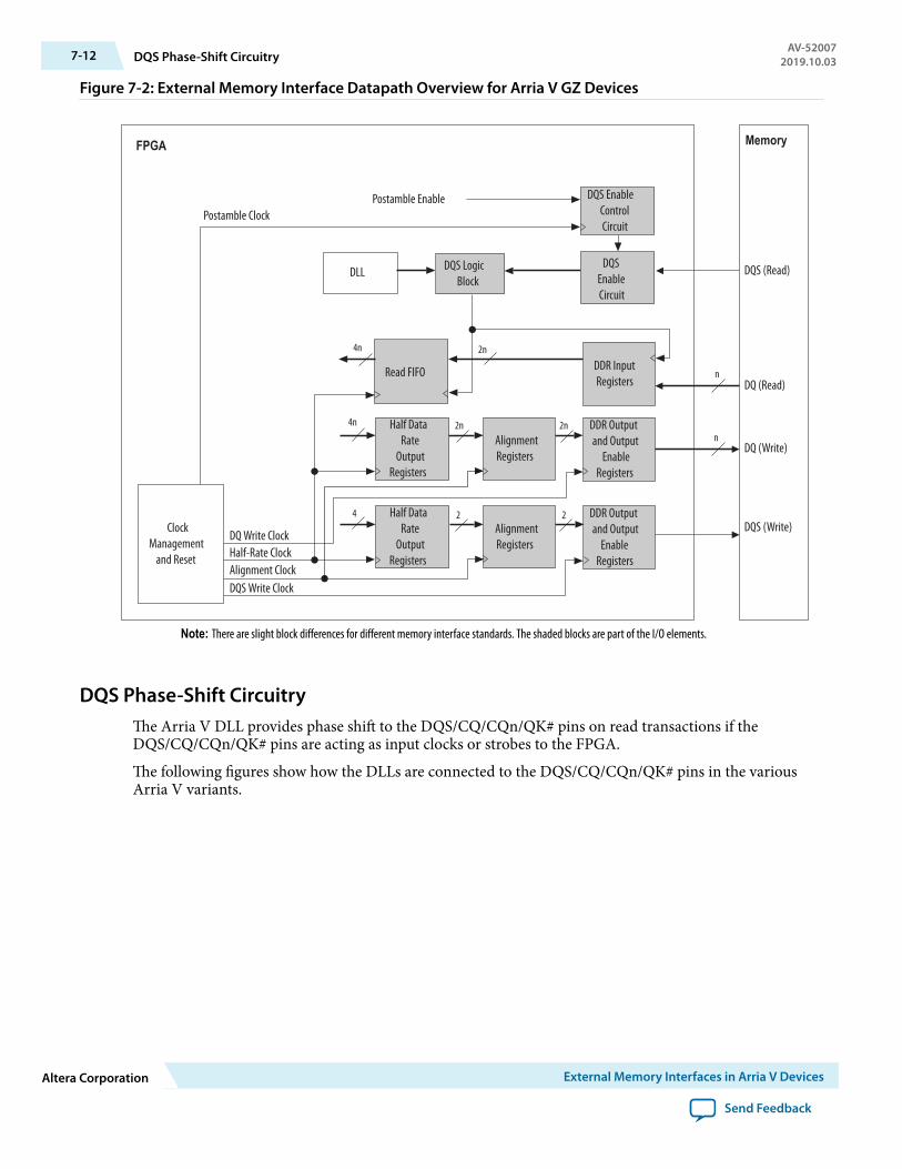
Figure 7-2: External Memory Interface Datapath Overview for Arria V GZ Devices
MemoryFPGA
DLL
4nn
n
2n
DQ (Read)
DQ (Write)
Read FIFO
DQS (Read)
4n
4DQS (Write)
DQS Write ClockAlignment ClockHalf-Rate Clock
2n 2n
2 2
DQ Write Clock
Postamble EnablePostamble Clock
DQS EnableControlCircuit
DQSEnableCircuit
DDR InputRegisters
DDR Outputand Output
EnableRegisters
DDR Outputand Output
Enable Registers
AlignmentRegisters
AlignmentRegisters
Half DataRate
OutputRegisters
Half DataRate
OutputRegisters
DQS LogicBlock
ClockManagement
and Reset
Note: There are slight block differences for different memory interface standards. The shaded blocks are part of the I/O elements.
DQS Phase-Shift CircuitryThe Arria V DLL provides phase shift to the DQS/CQ/CQn/QK# pins on read transactions if theDQS/CQ/CQn/QK# pins are acting as input clocks or strobes to the FPGA.
The following figures show how the DLLs are connected to the DQS/CQ/CQn/QK# pins in the variousArria V variants.
7-12 DQS Phase-Shift CircuitryAV-52007
2019.10.03
Altera Corporation External Memory Interfaces in Arria V Devices
Send Feedback
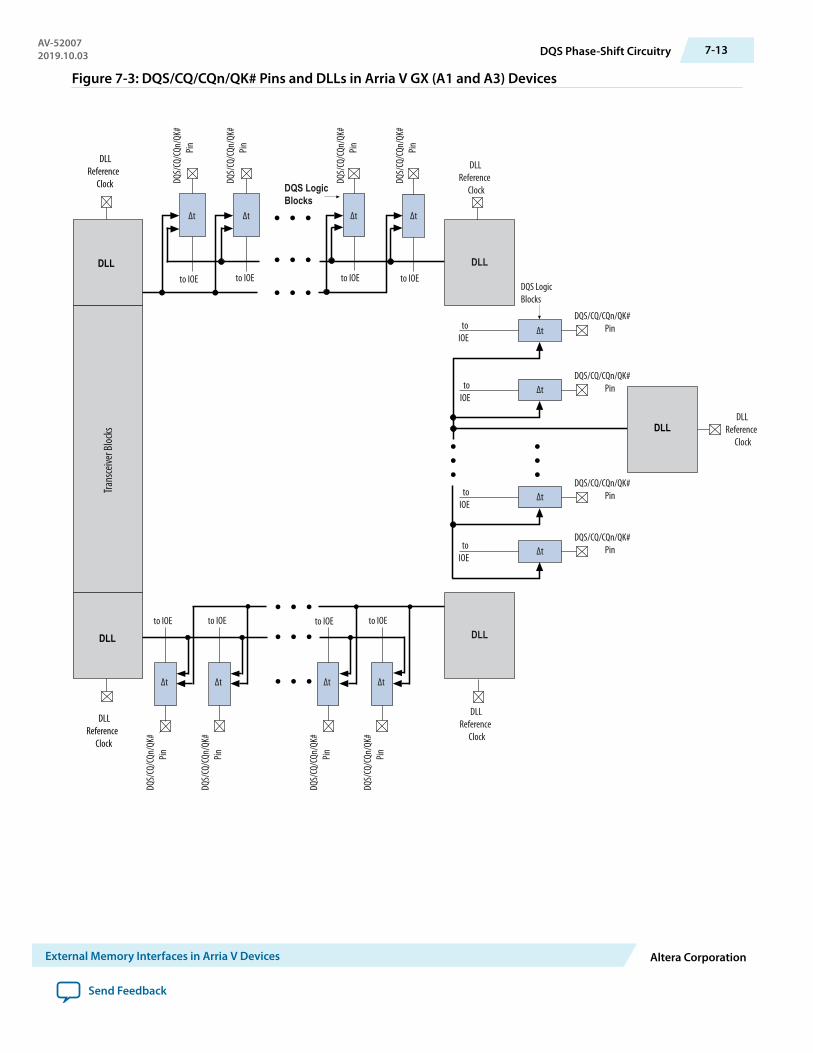
Figure 7-3: DQS/CQ/CQn/QK# Pins and DLLs in Arria V GX (A1 and A3) Devices
DLL
DLL
DLL
DLLReference
Clock
DLLReference
Clock
DLL Reference
Clock
DLL Reference
Clock
DQS/CQ/CQn/QK#Pin
DQS/
CQ/C
Qn/Q
K#Pin
DQS/
CQ/C
Qn/Q
K#Pin
DQS/
CQ/C
Qn/Q
K#Pin
DQS/
CQ/C
Qn/Q
K#Pin
DQS/
CQ/C
Qn/Q
K#Pin
DQS/
CQ/C
Qn/Q
K#Pin
DQS/
CQ/C
Qn/Q
K#Pin
DQS/
CQ/C
Qn/Q
K#Pin
DQS/CQ/CQn/QK#Pin
DQS/CQ/CQn/QK#Pin
DQS/CQ/CQn/QK#Pin
to IOE to IOE to IOE to IOE
DQS LogicBlocks
to IOE to IOEto IOEto IOE
Δt
Δt
Δt
ΔtΔtΔtΔt
Δt
ΔtΔtΔtΔt
DQS LogicBlocks
DLL Reference
Clock
DLL
to IOE
to IOE
to IOE
to IOE
DLL
Trans
ceive
r Bloc
ks
AV-520072019.10.03 DQS Phase-Shift Circuitry 7-13
External Memory Interfaces in Arria V Devices Altera Corporation
Send Feedback
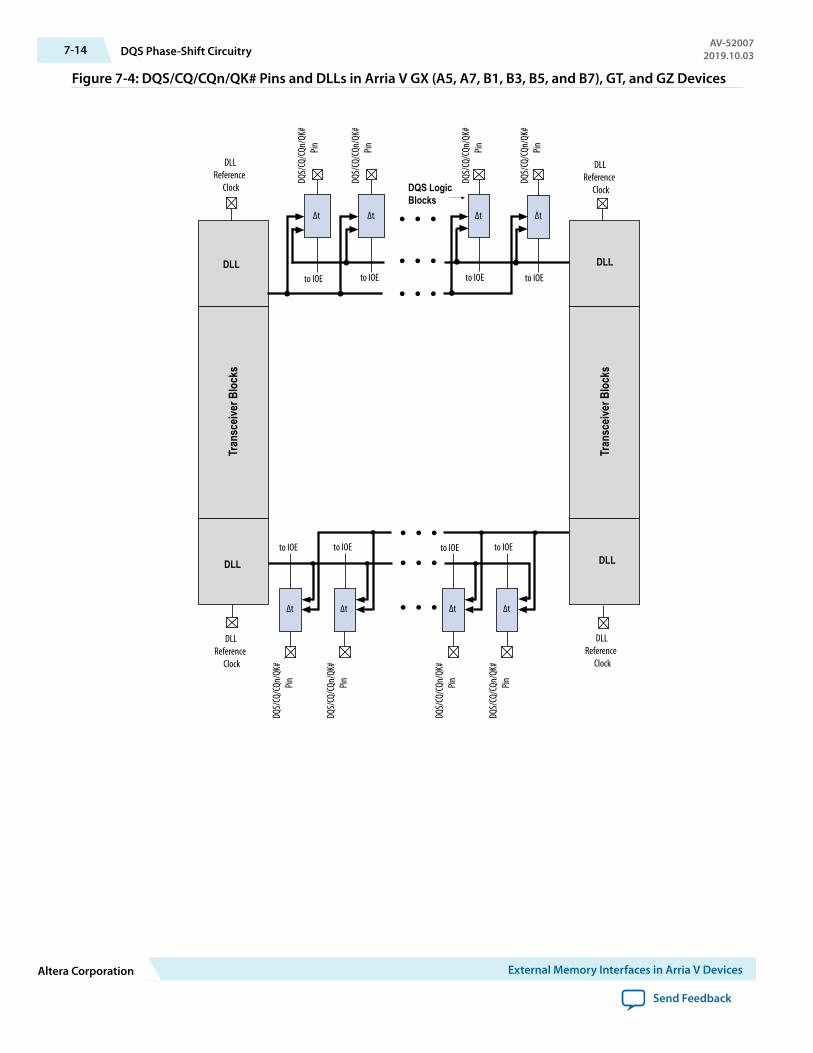
Figure 7-4: DQS/CQ/CQn/QK# Pins and DLLs in Arria V GX (A5, A7, B1, B3, B5, and B7), GT, and GZ Devices
DLL Reference
Clock
DLL Reference
Clock
to IOE to IOE to IOE to IOE
DQS LogicBlocks
ΔtΔtΔtΔt
DLLDLL
DLL Reference
Clock
to IOE to IOEto IOEto IOE
ΔtΔtΔtΔt
DLL Reference
Clock
DLLDLL
Tran
sceiv
er B
lock
s
Tran
sceiv
er B
lock
s
DQS/
CQ/C
Qn/Q
K#Pin
DQS/
CQ/C
Qn/Q
K#Pin
DQS/
CQ/C
Qn/Q
K#Pin
DQS/
CQ/C
Qn/Q
K#Pin
DQS/
CQ/C
Qn/Q
K#Pin
DQS/
CQ/C
Qn/Q
K#Pin
DQS/
CQ/C
Qn/Q
K#Pin
DQS/
CQ/C
Qn/Q
K#Pin
7-14 DQS Phase-Shift CircuitryAV-52007
2019.10.03
Altera Corporation External Memory Interfaces in Arria V Devices
Send Feedback

Figure 7-5: DQS/CQ/CQn/QK# Pins and DLLs in Arria V SX and ST Devices
Δt
Δt
DQS LogicBlocks
DQSPin
DQSPin
DLL Reference
Clock
to IOE to IOE
to IOE
to IOE
ΔtΔt
DLLHPS I/ODLL
DLL Reference
Clock
to IOE to IOEto IOEto IOE
ΔtΔtΔtΔt
DLL Reference
Clock
DLLDLL
Tran
sceiv
er B
lock
s
Tran
sceiv
er B
lock
s
HPS Block
HPSPLL
DQS/
CQ/C
Qn/Q
K#Pin
DQS/
CQ/C
Qn/Q
K#Pin
DQS/
CQ/C
Qn/Q
K#Pin
DQS/
CQ/C
Qn/Q
K#Pin
DQS/
CQ/C
Qn/Q
K#Pin
DQS/
CQ/C
Qn/Q
K#Pin
Delay-Locked Loop
The delay-locked loop (DLL) uses a frequency reference to dynamically generate control signals for thedelay chains in each of the DQS/CQ/CQn/QK# pins, allowing the delay to compensate for process,voltage, and temperature (PVT) variations. The DQS delay settings are gray-coded to reduce jitter if theDLL updates the settings.
There are a maximum of five DLLs in Arria V devices. You can clock each DLL using different frequencies.
AV-520072019.10.03 Delay-Locked Loop 7-15
External Memory Interfaces in Arria V Devices Altera Corporation
Send Feedback

Some of the DLLs can access the two adjacent sides from its location in the device. You can have twodifferent interfaces with the same frequency on the two sides adjacent to a DLL, where the DLL controlsthe DQS delay settings for both interfaces.
I/O banks between two DLLs have the flexibility to create multiple frequencies and multiple-typeinterfaces. These banks can use settings from either or both adjacent DLLs. For example, DQS1R can get itsphase-shift settings from DLL_TR, while DQS2R can get its phase-shift settings from DLL_BR.
The reference clock for each DLL may come from the PLL output clocks or clock input pins.
Note: If you have a dedicated PLL that only generates the DLL input reference clock, set the PLL mode toNo Compensation to achieve better performance (or the Intel Quartus Prime software automati‐cally changes it). Because the PLL does not use any other outputs, it does not have to compensatefor any clock paths.
DLL Reference Clock Input for Arria V Devices
Table 7-11: DLL Reference Clock Input from PLL Counter Outputs for Arria V GX A1 and A3, and Arria V GTC3 Devices—Preliminary
DLLPLL
1L 0L RC TC BC
DLL_T0 plldout[1:0] — — plldout[1:0] —
DLL_T1 — — — plldout[1:0] —
DLL_B0 — plldout[1:0] — — plldout[1:0]
DLL_B1 — — — — plldout[1:0]
DLL_R0 — — plldout[1:0] — —
Table 7-12: DLL Reference Clock Input from PLL Counter Outputs for Arria V GX A5, A7, B1, and B3, andArria V GT C7 and D3 Devices—Preliminary
DLLPLL
TL TR BR BL TC BC
DLL_T0 plldout[1:0
]
— — — plldout[1:0
]
—
DLL_T1 — plldout[1:0
]— — plldout[1:0
]
—
DLL_B0 — — — plldout[1:0
]
— plldout[1:0]
7-16 DLL Reference Clock Input for Arria V DevicesAV-52007
2019.10.03
Altera Corporation External Memory Interfaces in Arria V Devices
Send Feedback

DLLPLL
TL TR BR BL TC BC
DLL_B1 — — plldout[1:0
]
— — plldout[1:0]
Table 7-13: DLL Reference Clock Input from PLL Counter Outputs for Arria V GX B5 and B7, and Arria V GTD7 Devices—Preliminary
DLLPLL
2L 2R 0R 0L TC BC
DLL_T0 plldout[1:0
]
— — — plldout[1:0
]
—
DLL_T1 — plldout[1:0
]
— — plldout[1:0
]
—
DLL_B0 — — — plldout[1:0
]
— plldout[1:0]
DLL_B1 — — plldout[1:0
]
— — plldout[1:0]
Table 7-14: DLL Reference Clock Input for Arria V GZ E1 and E3 Devices
DLLPLL CLKIN
Center Corner Left Center Right
DLL_TL CEN_X84_Y77
CEN_X84_Y68
COR_X0_Y81
COR_X0_Y72
CLK20P
CLK21P
CLK22P
CLK23P
CLK16P
CLK17P
CLK18P
CLK19P
—
DLL_TR CEN_X84_Y77
CEN_X84_Y68
COR_X185_Y81
COR_X185_Y72
— CLK16P
CLK17P
CLK18P
CLK19P
CLK12P
CLK13P
CLK14P
CLK15P
AV-520072019.10.03 DLL Reference Clock Input for Arria V Devices 7-17
External Memory Interfaces in Arria V Devices Altera Corporation
Send Feedback

DLLPLL CLKIN
Center Corner Left Center Right
DLL_BR CEN_X84_Y11
CEN_X84_Y2
COR_X185_Y10
COR_X185_Y1
— CLK4P
CLK5P
CLK6P
CLK7P
CLK8P
CLK9P
CLK10P
CLK11P
DLL_BL CEN_X84_Y11
CEN_X84_Y2
COR_X0_Y10
COR_X0_Y1
CLK0P
CLK1P
CLK2P
CLK3P
CLK4P
CLK5P
CLK6P
CLK7P
—
Table 7-15: DLL Reference Clock Input for Arria V GZ E5 and E7 Devices
DLLPLL CLKIN
Center Corner Left Center Right
DLL_TL CEN_X92_Y96
CEN_X92_Y87
COR_X0_Y100
COR_X0_Y91
CLK20P
CLK21P
CLK22P
CLK23P
CLK16P
CLK17P
CLK18P
CLK19P
—
DLL_TR CEN_X92_Y96
CEN_X92_Y87
COR_X202_Y100
COR_X202_Y91
— CLK16P
CLK17P
CLK18P
CLK19P
CLK12P
CLK13P
CLK14P
CLK15P
DLL_BR CEN_X92_Y11
CEN_X92_Y2
COR_X202_Y10
COR_X202_Y1
— CLK4P
CLK5P
CLK6P
CLK7P
CLK8P
CLK9P
CLK10P
CLK11P
DLL_BL CEN_X92_Y11
CEN_X92_Y1
COR_X0_Y10
COR_X0_Y1
CLK0P
CLK1P
CLK2P
CLK3P
CLK4P
CLK5P
CLK6P
CLK7P
—
7-18 DLL Reference Clock Input for Arria V DevicesAV-52007
2019.10.03
Altera Corporation External Memory Interfaces in Arria V Devices
Send Feedback
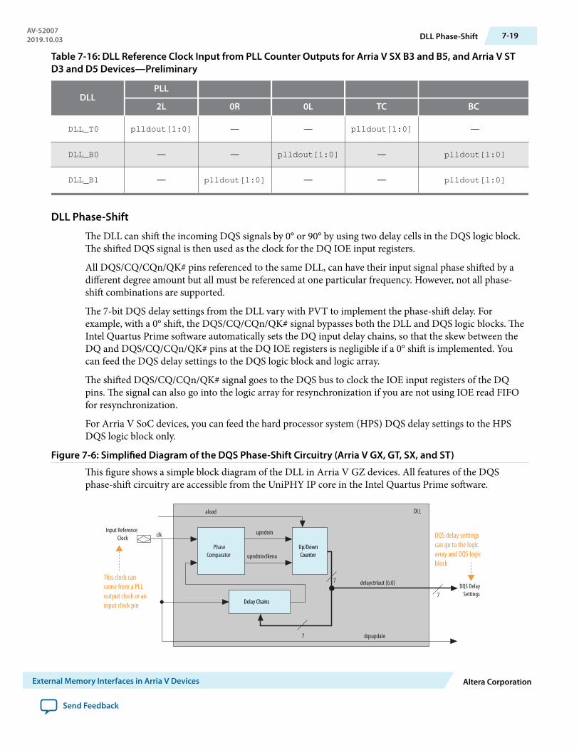
Table 7-16: DLL Reference Clock Input from PLL Counter Outputs for Arria V SX B3 and B5, and Arria V STD3 and D5 Devices—Preliminary
DLLPLL
2L 0R 0L TC BC
DLL_T0 plldout[1:0] — — plldout[1:0] —
DLL_B0 — — plldout[1:0] — plldout[1:0]
DLL_B1 — plldout[1:0] — — plldout[1:0]
DLL Phase-Shift
The DLL can shift the incoming DQS signals by 0° or 90° by using two delay cells in the DQS logic block.The shifted DQS signal is then used as the clock for the DQ IOE input registers.
All DQS/CQ/CQn/QK# pins referenced to the same DLL, can have their input signal phase shifted by adifferent degree amount but all must be referenced at one particular frequency. However, not all phase-shift combinations are supported.
The 7-bit DQS delay settings from the DLL vary with PVT to implement the phase-shift delay. Forexample, with a 0° shift, the DQS/CQ/CQn/QK# signal bypasses both the DLL and DQS logic blocks. TheIntel Quartus Prime software automatically sets the DQ input delay chains, so that the skew between theDQ and DQS/CQ/CQn/QK# pins at the DQ IOE registers is negligible if a 0° shift is implemented. Youcan feed the DQS delay settings to the DQS logic block and logic array.
The shifted DQS/CQ/CQn/QK# signal goes to the DQS bus to clock the IOE input registers of the DQpins. The signal can also go into the logic array for resynchronization if you are not using IOE read FIFOfor resynchronization.
For Arria V SoC devices, you can feed the hard processor system (HPS) DQS delay settings to the HPSDQS logic block only.
Figure 7-6: Simplified Diagram of the DQS Phase-Shift Circuitry (Arria V GX, GT, SX, and ST)
This figure shows a simple block diagram of the DLL in Arria V GZ devices. All features of the DQSphase-shift circuitry are accessible from the UniPHY IP core in the Intel Quartus Prime software.
7
7
7
delayctrlout [6:0]
dqsupdate
aload
clk upndnin
upndninclkena
DLL
This clock can come from a PLL output clock or an input clock pin
DQS delay settings can go to the logic array and DQS logic block
PhaseComparator
Up/DownCounter
Delay Chains
DQS DelaySettings
Input ReferenceClock
AV-520072019.10.03 DLL Phase-Shift 7-19
External Memory Interfaces in Arria V Devices Altera Corporation
Send Feedback

Figure 7-7: Simplified Diagram of the DQS Phase-Shift Circuitry (Arria V GZ)
This figure shows a simple block diagram of the DLL in Arria V GZ devices. All features of the DQSphase-shift circuitry are accessible from the UniPHY IP core in the Intel Quartus Prime software.
7
7
7PhaseOffset
Control A
7
Phase offset settingsfrom the logic array
Phase offsetsettings to DQS pins
DQS DelaySettings
delayctrlout[6:0]
offsetdelayctrlout[6:0]
offsetdelayctrlout[6:0]
dqsupdate
aload
clk upndnin
upndninclkena
DLL
7
PhaseComparator
Delay Chains
7
PhaseOffset
Control B
Phase offset settingsfrom the logic array
Phase offsetsettings to DQS pin
7
addnsub
(dll_offset_ctrl_a)
(dll_offset_ctrl_b)
addnsub
(offset[6:0])
( offset [6:0] )
(offsetctrlout[6:0])
(offsetctrlout[6:0])
offsetdelayctrlin[6:0]
offsetdelayctrlin[6:0]
Up/DownCounter
Phase offset settings can only go to the DQS logic blocks
DQS delay settings can go to the logic array and DQS logic block
This clock can come from a PLL output clock or an input clock pin
Input Reference Clock
The input reference clock goes into the DLL to a chain of up to eight delay elements. The phasecomparator compares the signal coming out of the end of the delay chain block to the input referenceclock. The phase comparator then issues the upndn signal to the Gray-code counter. This signal incrementsor decrements a 7-bit delay setting (DQS delay settings) that increases or decreases the delay through thedelay element chain to bring the input reference clock and the signals coming out of the delay elementchain in phase.
The DLL can be reset from either the logic array or a user I/O pin. Each time the DLL is reset, you mustwait for 2,560 clock cycles for the DLL to lock before you can capture the data properly. The DLL phasecomparator requires 2,560 clock cycles to lock and calculate the correct input clock period.
For the frequency range of each DLL frequency mode, refer to the device datasheet.
Related Information
• Arria V GX, GT, SX, and ST Device Datasheet• Arria V GZ Device Datasheet
PHY Clock (PHYCLK) NetworksThe PHYCLK network is a dedicated high-speed, low-skew balanced clock tree designed for a high-performance external memory interface.
The top and bottom sides of the Arria V devices have up to four PHYCLK networks. There are up to twoPHYCLK networks on the left and right side I/O banks. Each PHYCLK network spans across one I/Obank and is driven by one of the PLLs located adjacent to the I/O bank.
The following figures show the PHYCLK networks available in the Arria V devices.
7-20 PHY Clock (PHYCLK) NetworksAV-52007
2019.10.03
Altera Corporation External Memory Interfaces in Arria V Devices
Send Feedback

Figure 7-8: PHYCLK Networks in Arria V GX A1 and A3 Devices
LeftPLL
CenterPLL Sub-BankSub-Bank
I/O Bank 7Sub-BankSub-Bank
I/O Bank 8
PHYCLK Networks
LeftPLL
CenterPLL
Sub-BankSub-Bank
I/O Bank 4Sub-BankSub-Bank
I/O Bank 3
PHYCLK Networks
Cent
erPL
LSu
b-Ba
nkSu
b-Ba
nk I/O B
ank 6
Sub-
Bank
Sub-
Bank I/O
Ban
k 5
PHYC
LK N
etwo
rks
Tran
sceiv
er B
anks
FPGA Device
AV-520072019.10.03 PHY Clock (PHYCLK) Networks 7-21
External Memory Interfaces in Arria V Devices Altera Corporation
Send Feedback

Figure 7-9: PHYCLK Networks in Arria V GX A5, A7, B1, B3, B5, and B7 Devices, and Arria V GZ E1, E3, E5, andE7 Devices
LeftPLL
CenterPLL Sub-BankSub-Bank
I/O Bank 7Sub-BankSub-Bank
I/O Bank 8
PHYCLK Networks
LeftPLL
RightPLL
RightPLL
CenterPLL
Sub-BankSub-Bank
I/O Bank 4Sub-BankSub-Bank
I/O Bank 3
PHYCLK Networks
Tran
sceiv
er B
anks
Tran
sceiv
er B
anks
FPGA Device
7-22 PHY Clock (PHYCLK) NetworksAV-52007
2019.10.03
Altera Corporation External Memory Interfaces in Arria V Devices
Send Feedback
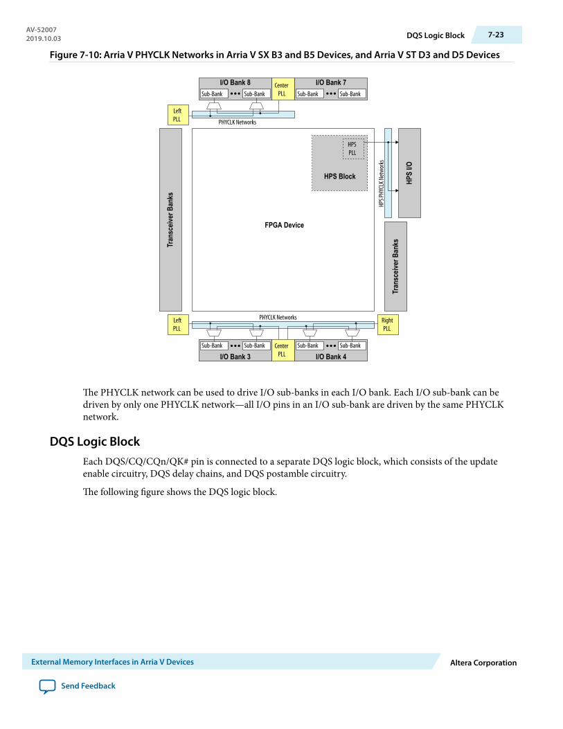
Figure 7-10: Arria V PHYCLK Networks in Arria V SX B3 and B5 Devices, and Arria V ST D3 and D5 Devices
LeftPLL
CenterPLL Sub-BankSub-Bank
I/O Bank 7Sub-BankSub-Bank
I/O Bank 8
PHYCLK Networks
HPS P
HYCL
K Net
work
s
LeftPLL
RightPLL
CenterPLL
Sub-BankSub-Bank
I/O Bank 4Sub-BankSub-Bank
I/O Bank 3
PHYCLK Networks
Tran
sceiv
er B
anks
Tran
sceiv
er B
anks
HPS
I/O
FPGA Device
HPSPLL
HPS Block
The PHYCLK network can be used to drive I/O sub-banks in each I/O bank. Each I/O sub-bank can bedriven by only one PHYCLK network—all I/O pins in an I/O sub-bank are driven by the same PHYCLKnetwork.
DQS Logic BlockEach DQS/CQ/CQn/QK# pin is connected to a separate DQS logic block, which consists of the updateenable circuitry, DQS delay chains, and DQS postamble circuitry.
The following figure shows the DQS logic block.
AV-520072019.10.03 DQS Logic Block 7-23
External Memory Interfaces in Arria V Devices Altera Corporation
Send Feedback
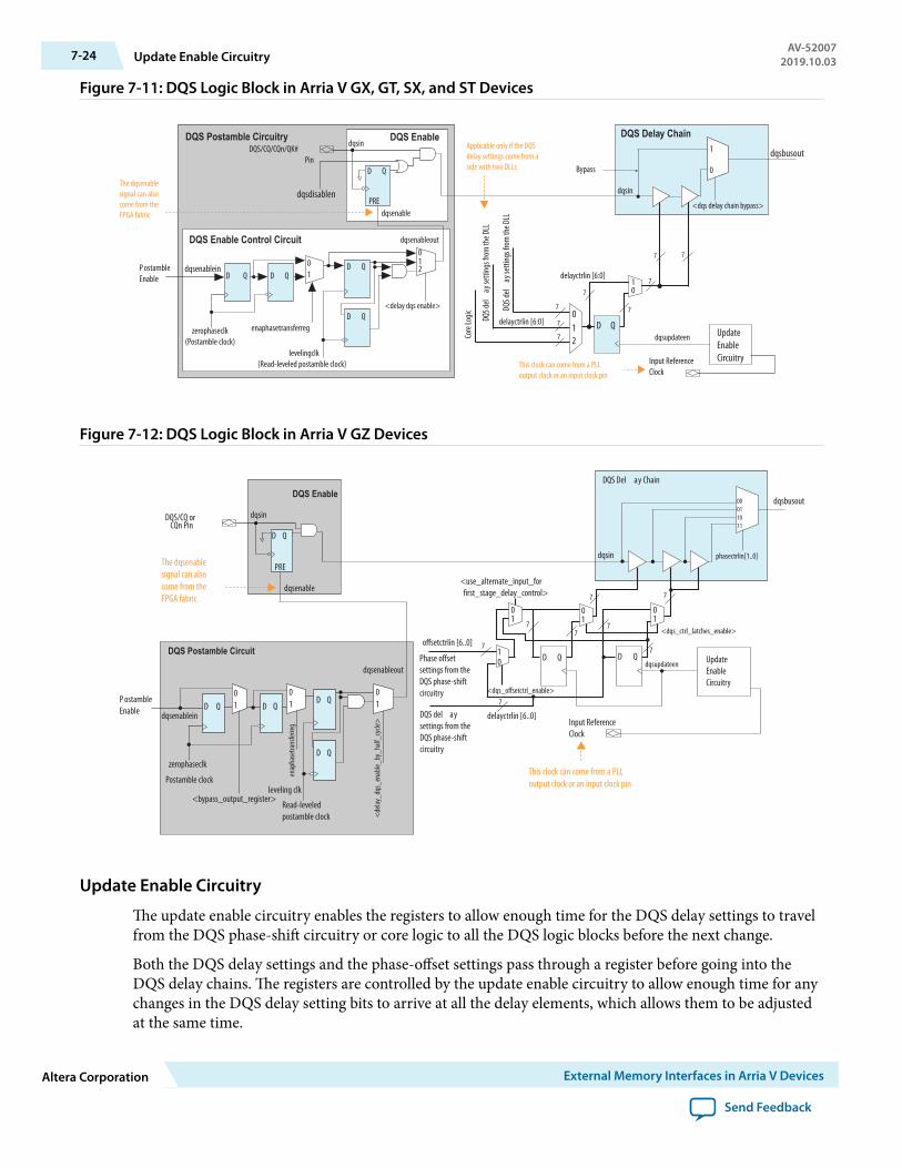
Figure 7-11: DQS Logic Block in Arria V GX, GT, SX, and ST Devices
UpdateEnableCircuitry
77
7
7
dqsin
delayctrlin [6:0]
dqsupdateen
DQS Delay Chain
Bypass
7
dqsbusout1
0
01
10
Input ReferenceClock
P ostambleEnable
dqsenablein
zerophaseclk(Postamble clock)
dqsenableout
levelingclk(Read-leveled postamble clock)
DQS Enable Control Circuit
DQS/CQ/CQn/QK# Pin
DQS Enabledqsin
D Q
PRE
01
dqsenable
D Q D QD Q
D Q
DQS Postamble Circuitry
D Q
7
7
DQS d
elay
setti
ngs f
rom
the D
LL
delayctrlin [6:0]
2
DQS d
elay
setti
ngs f
rom
the D
LL
Core
Logic
7
<dqs delay chain bypass>
enaphasetransferreg
012
<delay dqs enable>
dqsdisablen
This clock can come from a PLL output clock or an input clock pin
Applicable only if the DQS delay settings come from a side with two DLLs
The dqsenable signal can also come from the FPGA fabric
Figure 7-12: DQS Logic Block in Arria V GZ Devices
DD UpdateEnableCircuitry
7 7
7
7
7 7
DQS del aysettings from theDQS phase-shiftcircuitry
dqsin
delayctrlin [6..0]
offsetctrlin [6..0]
<dqs_offsetctrl_enable>
dqsupdateen
<dqs_ctrl_latches_enable>
phasectrlin[1..0]
DQS Del ay Chain
7
dqsbusout00011011
01
01
710 QQ
Input ReferenceClock
Phase offsetsettings from theDQS phase-shiftcircuitry
DQS/CQ orCQn Pin
DQS Enable
dqsin
D Q
PRE
dqsenable
P ostambleEnable dqsenablein
Postamble clock
zerophaseclk
dqsenableout
enap
hase
trans
ferre
g
leveling clk
Read-leveledpostamble clock <
delay
_dqs
_ena
ble_b
y_ha
lf_cy
cle>
DQS Postamble Circuit
01
01D Q D Q
D Q
D Q
01
<bypass_output_register>
01
<use_alternate_input_for first_stage_delay_control>
This clock can come from a PLL output clock or an input clock pin
The dqsenable signal can also come from the FPGA fabric
Update Enable Circuitry
The update enable circuitry enables the registers to allow enough time for the DQS delay settings to travelfrom the DQS phase-shift circuitry or core logic to all the DQS logic blocks before the next change.
Both the DQS delay settings and the phase-offset settings pass through a register before going into theDQS delay chains. The registers are controlled by the update enable circuitry to allow enough time for anychanges in the DQS delay setting bits to arrive at all the delay elements, which allows them to be adjustedat the same time.
7-24 Update Enable CircuitryAV-52007
2019.10.03
Altera Corporation External Memory Interfaces in Arria V Devices
Send Feedback

The circuitry uses the input reference clock or a user clock from the core to generate the update enableoutput. The UniPHY intellectual property (IP) uses this circuit by default.
Figure 7-13: DQS Update Enable Waveform
This figure shows an example waveform of the update enable circuitry output.
Update Enable Circuitry Output
System Clock
DQS Delay SettingsUpdated every 8 cycles
DLL Counter Update(Every 8 cycles)
7 bit
DLL Counter Update(Every 8 cycles)
DQS Delay Chain
DQS delay chains consist of a set of variable delay elements to allow the input DQS/CQ/CQn/QK# signalsto be shifted by the amount specified by the DQS phase-shift circuitry or the logic array.
There are two delay elements in the DQS delay chain that have the same characteristics:
• Delay elements in the DQS logic block• Delay elements in the DLL
The DQS/CQ/CQn/QK# pin is shifted by the DQS delay settings.
The number of delay chains required is transparent because the UniPHY IP automatically sets it when youchoose the operating frequency.
In Arria V GX, GT, and GZ devices, if you do not use the DLL to control the DQS delay chains, you caninput your own gray-coded 7 bit settings using the delayctrlin[6..0] signals available in the UniPHYIP.
In the Arria V SX and ST devices, the DQS delay chain is controlled by the DQS phase-shift circuitry only.
Related Information
• ALTDQ_DQS2 IP Core User GuideProvides more information about programming the delay chains.
• Delay Chains on page 7-31
DQS Postamble Circuitry
There are preamble and postamble specifications for both read and write operations in DDR3 and DDR2SDRAM. The DQS postamble circuitry ensures that data is not lost if there is noise on the DQS line duringthe end of a read operation that occurs while DQS is in a postamble state.
The Arria V devices contain dedicated postamble registers that you can control to ground the shifted DQSsignal that is used to clock the DQ input registers at the end of a read operation. This function ensures thatany glitches on the DQS input signal during the end of a read operation and occurring while DQS is in apostamble state do not affect the DQ IOE registers.
AV-520072019.10.03 DQS Delay Chain 7-25
External Memory Interfaces in Arria V Devices Altera Corporation
Send Feedback

• For preamble state, the DQS is low, just after a high-impedance state.• For postamble state, the DQS is low, just before it returns to a high-impedance state.
For external memory interfaces that use a bidirectional read strobe (DDR3 and DDR2 SDRAM), the DQSsignal is low before going to or coming from a high-impedance state.
Half Data Rate Block
The Arria V devices contain a half data rate (HDR) block in the postamble enable circuitry.
The HDR block is clocked by the half-rate resynchronization clock, which is the output of the I/O clockdivider circuit. There is an AND gate after the postamble register outputs to avoid postamble glitches froma previous read burst on a non-consecutive read burst. This scheme allows half-a-clock cycle latency fordqsenable assertion and zero latency for dqsenable deassertion.
Using the HDR block as the first stage capture register in the postamble enable circuitry block is optional.Altera recommends using these registers if the controller is running at half the frequency of the I/Os.
Figure 7-14: Avoiding Glitch on a Non-Consecutive Read Burst Waveform
This figure shows how to avoid postamble glitches using the HDR block.
Delayed by 1/2T logic
PreamblePostamble
Postamble glitch
DQS
Postamble Enable
dqsenable
Leveling Circuitry for Arria V GZ DevicesDDR3 SDRAM unbuffered modules use a fly-by clock distribution topology for better signal integrity. Thismeans that the CK/CK# signals arrive at each DDR3 SDRAM device in the module at different times. Thedifference in arrival time between the first DDR3 SDRAM device and the last device on the module can beas long as 1.6 ns.
The following figure shows the clock topology in DDR3 SDRAM unbuffered modules.
7-26 Half Data Rate BlockAV-52007
2019.10.03
Altera Corporation External Memory Interfaces in Arria V Devices
Send Feedback

Figure 7-15: DDR3 SDRAM Unbuffered Module Clock Topology
DQS/DQ DQS/DQDQS/DQDQS/DQDQS/DQ DQS/DQ CK/CK#
FPGA
DQS/DQ DQS/DQ
Because the data and read strobe signals are still point-to-point, take special care to ensure that the timingrelationship between the CK/CK# and DQS signals (tDQSS, tDSS, and tDSH) during a write is met at everydevice on the modules. In a similar way, read data coming back into the FPGA from the memory is alsostaggered.
The Arria V GZ devices have leveling circuitry to address these two situations. There is one leveling circuitper I/O sub-bank (for example, I/O sub-bank 1A, 1B, and 1C each has one leveling circuitry). These delaychains are PVT-compensated by the same DQS delay settings as the DLL and DQS delay chains.
The DLL uses eight delay chain taps, such that each delay chain tap generates a 45° delay. The generatedclock phases are distributed to every DQS logic block that is available in the I/O sub-bank. The delay chaintaps then feed a multiplexer controlled by the UniPHY IP core to select which clock phases are to be usedfor that x4 or x 8 DQS group. Each group can use a different tap output from the read-leveling and write-leveling delay chains to compensate for the different CK/CK# delay going into each device on the module.
Figure 7-16: Write-Leveling Delay Chains and Multiplexers
There is one leveling delay chain per I/O sub-bank (for example, I/O sub-banks 1A, 1B, and 1C). You canonly have one memory interface in each I/O sub-bank when you use the leveling delay chain.
Write clk(-900) Write-Leveled DQS Clock
Write-Leveled DQ Clock
The –90° write clock of the UniPHY IP feeds the write-leveling circuitry to produce the clock to generatethe DQS and DQ signals. During initialization, the UniPHY IP picks the correct write-leveled clock for the
AV-520072019.10.03 Leveling Circuitry for Arria V GZ Devices 7-27
External Memory Interfaces in Arria V Devices Altera Corporation
Send Feedback
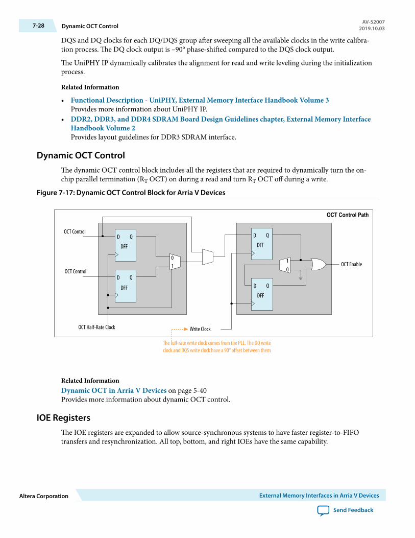
DQS and DQ clocks for each DQ/DQS group after sweeping all the available clocks in the write calibra‐tion process. The DQ clock output is –90° phase-shifted compared to the DQS clock output.
The UniPHY IP dynamically calibrates the alignment for read and write leveling during the initializationprocess.
Related Information
• Functional Description - UniPHY, External Memory Interface Handbook Volume 3Provides more information about UniPHY IP.
• DDR2, DDR3, and DDR4 SDRAM Board Design Guidelines chapter, External Memory InterfaceHandbook Volume 2Provides layout guidelines for DDR3 SDRAM interface.
Dynamic OCT ControlThe dynamic OCT control block includes all the registers that are required to dynamically turn the on-chip parallel termination (RT OCT) on during a read and turn RT OCT off during a write.
Figure 7-17: Dynamic OCT Control Block for Arria V Devices
DFF
D Q
D Q
DFF
OCT Control
OCT Control
OCT Half-Rate Clock
01
D Q
DFF
D Q
DFF
10
Write Clock
OCT Enable
OCT Control Path
The full-rate write clock comes from the PLL. The DQ write clock and DQS write clock have a 90° offset between them
Related InformationDynamic OCT in Arria V Devices on page 5-40Provides more information about dynamic OCT control.
IOE RegistersThe IOE registers are expanded to allow source-synchronous systems to have faster register-to-FIFOtransfers and resynchronization. All top, bottom, and right IOEs have the same capability.
7-28 Dynamic OCT ControlAV-52007
2019.10.03
Altera Corporation External Memory Interfaces in Arria V Devices
Send Feedback
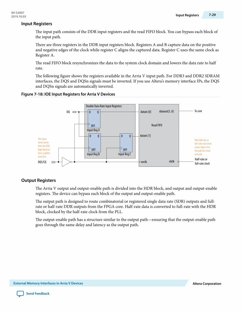
Input Registers
The input path consists of the DDR input registers and the read FIFO block. You can bypass each block ofthe input path.
There are three registers in the DDR input registers block. Registers A and B capture data on the positiveand negative edges of the clock while register C aligns the captured data. Register C uses the same clock asRegister A.
The read FIFO block resynchronizes the data to the system clock domain and lowers the data rate to halfrate.
The following figure shows the registers available in the Arria V input path. For DDR3 and DDR2 SDRAMinterfaces, the DQS and DQSn signals must be inverted. If you use Altera’s memory interface IPs, the DQSand DQSn signals are automatically inverted.
Figure 7-18: IOE Input Registers for Arria V Devices
Input Reg A
Input Reg B
D Q
Input Reg C
Double Data Rate Input Registers
Read FIFO
datain [1]
wrclk rdclk
datain [0] dataout[3..0] To core
Half-rate orfull-rate clockDQS/CQ
DQ D
DFF
Q
D
DFF
Q D
DFF
QThe input clock can be from the DQS logic block or from a global clock line.
This half-rate or full-rate read clock comes from a PLL through the clock network
Output Registers
The Arria V output and output-enable path is divided into the HDR block, and output and output-enableregisters. The device can bypass each block of the output and output-enable path.
The output path is designed to route combinatorial or registered single data rate (SDR) outputs and full-rate or half-rate DDR outputs from the FPGA core. Half-rate data is converted to full-rate with the HDRblock, clocked by the half-rate clock from the PLL.
The output-enable path has a structure similar to the output path—ensuring that the output-enable pathgoes through the same delay and latency as the output path.
AV-520072019.10.03 Input Registers 7-29
External Memory Interfaces in Arria V Devices Altera Corporation
Send Feedback

Figure 7-19: IOE Output and Output-Enable Path Registers for Arria V GX, GT, SX, and ST Devices
The following figure shows the registers available in the Arria V GX, GT, SX, and ST output and output-enable paths.
DFF
D Q
OE Reg A OE
DFF
D Q
OE Reg B OE
10
10
DFF
D Q
DFF
D Q
Half Data Rate to SingleData Rate Output-EnableRegisters
Double Data RateOutput-Enable Registers
10
DFF
D Q
DFF
D Q
Half Data Rate to SingleData Rate Output Registers
10
DFF
D Q
DFF
D Q
From Core
From Core
From Core(wdata2)
From Core(wdata0)
From Core(wdata3)
From Core(wdata1)
Half-Rate Clockfrom PLL
Write Clock
DFF
D Q
OE Reg A O
DFF
D Q
OE Reg B O
Double Data RateOutput Registers
10
DQ or DQS
Data coming from the FPGA core are at half the frequency of the memory interface clock frequency in half-rate mode
The full-rate write clock can come from the PLL. The DQ write clock have a 90° offset to the DQS write clock.
OR2
TRI
7-30 Output RegistersAV-52007
2019.10.03
Altera Corporation External Memory Interfaces in Arria V Devices
Send Feedback

Figure 7-20: IOE Output and Output-Enable Path Registers for Arria V GZ Devices
The following figure shows the registers available in the Arria V GZ output and output-enable paths. Youcan bypass each register block of the output and output-enable paths.
DFF
D Q
OE Reg A OE
DFF
D Q
OE Reg B OE
10
10
DFF
D Q
DFF
D Q
Double Data RateOutput-Enable Registers
10
DFF
D Q
DFF
D Q
10
DFF
D Q
DFF
D Q
From Core
From Core
From Core(wdata2)
From Core(wdata0)
From Core(wdata3)
From Core(wdata1)
Half-Rate Clock Write Clock
DFF
D Q
OE Reg A O
DFF
D Q
OE Reg B O
Double Data RateOutput Registers
10
DQ or DQS
Data coming from the FPGA core are at half the frequency of the memory interface clock frequency in half-rate mode
The write clock can come from either the PLL or from the write-leveling delay chain.The DQ write clock and DQS write clock have a 90° offset between them
Half Data Rate to Single Data Rate Output-Enable Registers
DFF
D Q
DFF
D Q
DFF
D Q
000001010011100101110111
DFF
D Q 10
DFF
D Q
DFF
D Q
DFF
D Q
000001010011100101110111
DFF
D Q 10
DFF
D Q
DFF
D Q
DFF
D Q
000001010011100101110111
DFF
D Q 10
enaphasetransferreg
enaphasetransferreg
enaphasetransferreg
dataout
dataout
dataout
enaoutputcycledelay[2..0]<add_output_cycle_delay>
enaoutputcycledelay[2..0]<add_output_cycle_delay>
enaoutputcycledelay[2..0]<add_output_cycle_delay>
Alignment Clock
Alignment Registers
Alignment Registers
From the PLL
From write-leveling delay chains
Used in DDR3 SDRAM interfacesfor write-leveling purposes
OR2
TRI
Half Data Rate to Single Data Rate Output Registers
Delay ChainsThe Arria V devices contain run-time adjustable delay chains in the I/O blocks and the DQS logic blocks.You can control the delay chain setting through the I/O or the DQS configuration block output.
AV-520072019.10.03 Delay Chains 7-31
External Memory Interfaces in Arria V Devices Altera Corporation
Send Feedback

Every I/O block contains a delay chain between the following elements:
• The output registers and output buffer• The input buffer and input register• The output enable and output buffer• The R T OCT enable-control register and output buffer
Figure 7-21: Delay Chains in an I/O Block in the Arria V GX, GT, SX, and ST Devices
D5 OCTdelaychain
OCT Enable Output Enable
D5output-enable
delay chain
D5 Delaydelay chain
D1 Delaydelay chain
01
DQ or DQS
7-32 Delay ChainsAV-52007
2019.10.03
Altera Corporation External Memory Interfaces in Arria V Devices
Send Feedback
Figure 7-22: Delay Chains in an I/O Block in Arria V GZ Devices
outputdelaysetting2
octdelaysetting1
rtena oe
octdelaysetting2
outputdelaysetting1
padtoinputregisterdelaysetting
padtoinputregisterrisefalldelaysetting[5..0]
01
D5 OCTdelay chain
D5 Ouput Enable
delay chain
D6 Ouput Enable
delay chain
D5 Delaydelay chain
D1 Delaydelay chain
D2 Delaydelay chain
D3 Delaydelay chain
D1 Rise/Fall Balancing
delay chain
D6 Delaydelay chain
D6 OCTdelay chain
DQ
Each DQS logic block contains a delay chain after the dqsbusout output and another delay chain beforethe dqsenable input.
Figure 7-23: Delay Chains in the DQS Input Path
DQSEnable
dqsin
dqsenable
DQS Enable Control
DQS delaychain D4
delay chain
dqsbusoutDQS
T11 delay chain
Related Information
• ALTDQ_DQS2 IP Core User GuideProvides more information about programming the delay chains.
• DQS Delay Chain on page 7-25
AV-520072019.10.03 Delay Chains 7-33
External Memory Interfaces in Arria V Devices Altera Corporation
Send Feedback

I/O and DQS Configuration BlocksThe I/O and DQS configuration blocks are shift registers that you can use to dynamically change thesettings of various device configuration bits.
• The shift registers power-up low.• Every I/O pin contains one I/O configuration register.• Every DQS pin contains one DQS configuration block in addition to the I/O configuration register.
Figure 7-24: Configuration Block (I/O and DQS)
This figure shows the I/O configuration block and the DQS configuration block circuitry.
datain
bit0bit1bit2MSB
dataoutupdate
ena
clk
rankselectreadrankselectwrite
Related InformationALTDQ_DQS2 IP Core User GuideProvides more information about programming the delay chains.
Hard Memory ControllerThe Arria V GX, GT, SX, and ST devices feature dedicated hard memory controllers. You can use the hardmemory controllers for DDR2 and DDR3 SDRAM interfaces. Compared to the memory controllersimplemented using core logic, the hard memory controllers allow support for higher memory interfacefrequencies with shorter latency cycles.
The hard memory controllers use dedicated I/O pins as data, address, command, control, clock, andground pins for the SDRAM interface. If you do not use the hard memory controllers, you can use thesededicated pins as regular I/O pins.
Note: There is no hard memory controller in the Arria V GZ devices.
Related Information
• Functional Description - HPC II Controller Chapter, ExternalThe hard memory controller is functionally similar to the High-Performance Controller II (HPC II).
• Functional Description - HPS Memory Controller, External Memory Interface Handbook Volume3Provides detailed information about application of the hard memory interface.
7-34 I/O and DQS Configuration BlocksAV-52007
2019.10.03
Altera Corporation External Memory Interfaces in Arria V Devices
Send Feedback

Features of the Hard Memory Controller
Table 7-17: Features of the Arria V Hard Memory Controller
Feature Description
MemoryInterface DataWidth
• 8, 16, and 32 bit data• 16 bit data + 8 bit ECC• 32 bit data + 8bit ECC
MemoryDensity
The controller supports up to four gigabits density parts and two chip selects.
MemoryBurst Length
• DDR3—Burst length of 8 and burst chop of 4• DDR2—Burst lengths of 4 and 8
Commandand DataReordering
The controller increases efficiency through the support for out-of-order execution ofDRAM commands—with address collision detection-and in-order return of results.
StarvationControl
A starvation counter ensures that all requests are served after a predefined time-outperiod. This function ensures that data with low priority access are not left behind whenreordering data for efficiency.
User-ConfigurablePrioritySupport
When the controller detects a high priority request, it allows the request to bypass thecurrent queuing request. This request is processed immediately and thus reduces latency.
Avalon®-MMData SlaveLocalInterface
By default, the controller supports the Avalon Memory-Mapped protocol.
BankManagement
By default, the controller provides closed-page bank management on every access. Thecontroller intelligently keeps a row open based on incoming traffic. This feature improvesthe efficiency of the controller especially for random traffic.
StreamingReads andWrites
The controller can issue reads or writes continuously to sequential addresses every clockcycle if the bank is open. This function allows for very high efficiencies with large amountsof data.
BankInterleaving
The controller can issue reads or writes continuously to 'random' addresses.
AV-520072019.10.03 Features of the Hard Memory Controller 7-35
External Memory Interfaces in Arria V Devices Altera Corporation
Send Feedback
Feature Description
PredictiveBankManagement
The controller can issue bank management commands early so that the correct row isopen when the read or write occurs. This increases efficiency.
MultiportInterface
The interface allows you to connect up to six data masters to access the memory controllerthrough the local interface. You can update the multiport scheduling configurationwithout interrupting traffic on a port.
Built-in BurstAdaptor
The controller can accept bursts of arbitrary sizes on its local interface and map thesebursts to efficient memory commands.
Run-timeConfigurationof theController
This feature provides support for updates to the timing parameters without requiringreconfiguration of the FPGA, apart from the standard compile-time setting of the timingparameters.
On-DieTermination
The controller controls the on-die termination (ODT) in the memory, which improvessignal integrity and simplifies your board design.
User-ControlledRefreshTiming
You can optionally control when refreshes occur—allowing the refreshes to avoid clashingof important reads or writes with the refresh lock-out time.
Low PowerModes
You can optionally request the controller to put the memory into the self-refresh or deeppower-down modes.
Partial ArraySelf-Refresh
You can select the region of memory to refresh during self-refresh through the moderegister to save power.
ECC Standard Hamming single error correction, double error detection (SECDED) errorcorrection code (ECC) support:
• 32 bit data + 8 bit ECC• 16 bit data + 8 bit ECC
AdditiveLatency
With additive latency, the controller can issue a READ/WRITE command after theACTIVATE command to the bank prior to t RCD to increase the command efficiency.
Caution: Efficiency degradation may occur when using the additive latency featurewith the hard memory controller for DDR3 SDRAM interfaces at 533 MHz.
WriteAcknowledg‐ment
The controller supports write acknowledgment on the local interface.
7-36 Features of the Hard Memory ControllerAV-52007
2019.10.03
Altera Corporation External Memory Interfaces in Arria V Devices
Send Feedback

Feature Description
User Controlof MemoryControllerInitialization
The controller supports initialization of the memory controller under the control of userlogic—for example, through the software control in the user system if a processor ispresent.
ControllerBondingSupport
You can bond two controllers to achieve wider data width for higher bandwidth applica‐tions.
Multi-Port Front EndThe multi-port front end (MPFE) and its associated fabric interface provide up to six command ports, fourread-data ports and four write-data ports, through which user logic can access the hard memorycontroller.
Figure 7-25: Simplified Diagram of the Arria V Hard Memory Interface
This figure shows a simplified diagram of the Arria V hard memory interface with the MPFE.
MPFEMemory
ControllerPHY Memory
FPGACore Logic
FPGA
Avalon-MM Interface AFI
Bonding SupportNote: Bonding is supported only for hard memory controllers configured with one port. Do not use the
bonding configuration when there is more than one port in each hard memory controller.
You can bond one port of any data width (64, 128, or 256 bits) from two hard memory controllers tosupport wider data widths.
If you bond two hard memory controllers, the data going out of the controllers to the user logic issynchronized. However, the data going out of the controllers to the memory is not synchronized.
The bonding controllers are not synchronized and remain independent with two separate address busesand two independent command buses. These buses are calibrated separately.
If you require ECC support for a bonded interface, you must implement the ECC logic external to the hardmemory controllers.
Note: Only one bonding feature is available per package through the core fabric. A memory interface thatuses the bonding feature has higher average latency.
AV-520072019.10.03 Multi-Port Front End 7-37
External Memory Interfaces in Arria V Devices Altera Corporation
Send Feedback
Figure 7-26: Hard Memory Controllers Bonding Support in Arria V GX A1 and A3 Devices
This figure shows the bonding of two opposite hard memory controllers through the core fabric.
Bond
ing(Co
re Ro
uting
)
16-bit Interface
Bank 8 Bank 7
Hard Memory Controller
16-bit Interface
Bank 4Bank 3
Hard Memory Controller
Bank
6Ba
nk 5
7-38 Bonding SupportAV-52007
2019.10.03
Altera Corporation External Memory Interfaces in Arria V Devices
Send Feedback
Figure 7-27: Hard Memory Controllers Bonding Support in Arria V GX A5, A7, B1, B3, B5, and B7 Devices,and Arria V GT D3 and D7 Devices
This figure shows the bonding of opposite and same side hard memory controllers through the core fabric.
Bond
ing(Co
re Ro
uting
)
Bonding(Core Routing)
Bonding(Core Routing)
Bond
ing(Co
re Ro
uting
)
32-bit Interface32-bit Interface
Bank 8 Bank 7
Hard Memory Controller Hard Memory Controller
32-bit Interface 32-bit Interface
Bank 4Bank 3
Hard Memory ControllerHard Memory Controller
Core routing is enabled only for single hard memory controller bond out per side. This bonding is available only if you do not use the hard memory controllers in banks 4 and 7 for bonding with other banks.
AV-520072019.10.03 Bonding Support 7-39
External Memory Interfaces in Arria V Devices Altera Corporation
Send Feedback

Figure 7-28: Hard Memory Controllers in Arria V SX B3 and B5 Devices, and Arria V ST D3 and D5 Devices
This figure shows the bonding of opposite and same side hard memory controllers through the core fabric.
Bank 8
32-bit DDR3 Interface
Bank 4Bank 3
Hard Memory Controller
Hard Memory Controller
32-bit DDR3 Interface
32-bit DDR3 Interface
Hard Memory Controller
HPS I
/O
HPS I/O
HPS Block
HPS H
ard M
emor
y Con
trolle
r
32-b
it DD
R3 In
terfa
ce
Bonding(Core Routing)
Bond
ing(Co
re Ro
uting
)
Enabled only for single hard memory controller bond out per side. This bonding is available only if you do not use the hard memory controllers in bank 3 for bonding with other banks.
No bonding support for the HPS hard memory controller.
Related Information
• Arria V GT and GX Device Family Pin Connection GuidelinesProvides more information about the dedicated pins.
• Bonding Does Not Work for Multiple MPFE Ports in Hard Memory Controller KDB
7-40 Bonding SupportAV-52007
2019.10.03
Altera Corporation External Memory Interfaces in Arria V Devices
Send Feedback

Hard Memory Controller Width for Arria V GX
Table 7-18: Hard Memory Controller Width Per Side in Arria V GX A1, A3, A5, and A7 Devices
Package
Member Code
A1 A3 A5 A7
Top Bottom Top Bottom Top Bottom Top Bottom
F672 16 16 16 16 32 32 32 32
F896 24 24 24 24 32 32 32 32
F1152 — — — — 32 + 32 32 + 32 32 + 32 32 + 32
Table 7-19: Hard Memory Controller Width Per Side in Arria V GX B1, B3, B5, and B7 Devices
Package
Member Code
B1 B3 B5 B7
Top Bottom Top Bottom Top Bottom Top Bottom
F896 32 32 32 32 — — — —
F1152 32 + 32 32 + 32 32 + 32 32 + 32 32 + 32 32 + 32 32 + 32 32 + 32
F1517 40 + 40 40 + 40 40 + 40 40 + 40 40 + 40 40 + 40 40 + 40 40 + 40
Related InformationArria V Device OverviewProvides more information about which device packages and feature options contain hard memorycontrollers.
Hard Memory Controller Width for Arria V GT
Table 7-20: Hard Memory Controller Width Per Side in Arria V GT Devices
Package
Member Code
C3 C7 D3 D7
Top Bottom Top Bottom Top Bottom Top Bottom
F672 16 16 16 16 — — — —
F896 24 24 24 24 24 24 — —
F1152 — — 32 + 32 32 + 32 32 + 32 32 + 32 32 + 32 32 + 32
F1157 — — — — 40 + 40 40 + 40 40 + 40 40 + 40
AV-520072019.10.03 Hard Memory Controller Width for Arria V GX 7-41
External Memory Interfaces in Arria V Devices Altera Corporation
Send Feedback

Related InformationArria V Device OverviewProvides more information about which device packages and feature options contain hard memorycontrollers.
Hard Memory Controller Width for Arria V SX
Table 7-21: FPGA Hard Memory Controller Width Per Side in Arria V SX Devices
Package
Member Code
B3 B5
Top Bottom Top Bottom
F896 24 24 — —
F1152 32 + 32 32 + 32 32 + 32 32 + 32
F1517 40 + 40 40 + 40 40 + 40 40 + 40
Related InformationArria V Device OverviewProvides more information about which device packages and feature options contain hard memorycontrollers.
Hard Memory Controller Width for Arria V ST
Table 7-22: FPGA Hard Memory Controller Width Per Side in Arria V ST Devices
Package
Member Code
D3
Top Bottom
F896 24 24
F1152 32 + 32 32 + 32
F1517 40 + 40 40 + 40
Related InformationArria V Device OverviewProvides more information about which device packages and feature options contain hard memorycontrollers.
7-42 Hard Memory Controller Width for Arria V SXAV-52007
2019.10.03
Altera Corporation External Memory Interfaces in Arria V Devices
Send Feedback
External Memory Interfaces in Arria V Devices Revision History
Date Version Changes
December2015
2015.12.21 Changed instances of Quartus II to Quartus Prime.
January 2015 2015.01.23 • Updated hard memory controller widths for all devices.• Removed "Preliminary" notes.
June 2014 2014.06.30 • Added links to the Arria V Device Overview for more informationabout which device feature option supports the hard memory control‐lers.
• Updated the hard memory controller widths for all devices where thewidths are 64, 72, and 80 bits. The widths are now updated to "32 +32", "40 + 32", and "40 + 40", respectively. The update is to clarify themaximum interface width per hard memory controller in the devices.
January 2014 2014.01.10 • Reduced the soft memory controller performance for DDR3 1.35 V inArria V GX, GT, SX, and ST devices from 667 MHz to 600 MHz.
• Removed support for DDR2 in the HPS hard memory controller.• Updated the figure that shows the delay chains in the Arria V GZ I/O
block.• Added related information link to ALTDQ_DQS2 Megafunction
User Guide for more information about using the delay chains.• Changed all "SoC FPGA" to "SoC".• Updated the figure that shows the DQS/CQ/CQn/QK# Pins and DLLs
in Arria V GX A1 and A3 to add the DLL reference clock to the leftside DLL.
• Updated the topic about delay-locked loop (DLL) to specify that thereis a maximum of five DLLs (instead of four).
• Updated the topic about the PHYCLK networks to add informationabout using the PHYCLK network to drive the I/O sub-banks in eachI/O bank.
• Added links to Altera's External Memory Spec Estimator tool to thetopics listing the external memory interface performance.
• Updated topic about hard memory controller bonding support tospecify that bonding is supported only for hard memory controllersconfigured with one port.
AV-520072019.10.03 External Memory Interfaces in Arria V Devices Revision History 7-43
External Memory Interfaces in Arria V Devices Altera Corporation
Send Feedback

Date Version Changes
May 2013 2013.05.06 • Moved all links to the Related Information section of respective topicsfor easy reference.
• Added link to the known document issues in the Knowledge Base.• Updated the topic about Arria V GZ leveling circuitry.• Removed the Arria V GZ phase offset control topic.• Added the I/O and DQS configuration blocks topic.• Updated the DQ/DQS groups for Arria V GX.• Added the DQ/DQS groups for Arria V GT C3 and C7.• Added the DLL reference clock input tables for all Arria V devices.• Added the FPGA hard memory controller widths for Arria V GX, GT,
SX, and ST.• Added the HPS hard memory controller widths for Arria V SX and
ST.
November2012
2012.11.19 • Reorganized content and updated template.• Added information for Arria V GZ, including a topic on the leveling
circuitry.• Added a list of supported external memory interface standards using
the hard memory controller and soft memory controller.• Added performance information for external memory interfaces and
the HPS external memory interfaces.• Separated the DQ/DQS groups tables into separate topics for each
device variant for easy reference.• Moved the PHYCLK networks pin placement guideline to the
Planning Pin and FPGA Resources chapter of the External MemoryInterface Handbook.
• Moved information from the "Design Considerations" section intorelevant topics.
• Removed the "DDR2 SDRAM Interface" and "DDR3 SDRAM DIMM"sections. Refer to the relevant sections in the External MemoryInterface Handbook for the information.
• Updated the diagram for DQS/CQ/CQn/QK# pins and DLLs in ArriaV GX A1 and A3 devices to add DLLs on the right, top left, andbottom left, and update the DLL connections to the pins.
• Updated the term "Multiport logic" to "multi-port front end" (MPFE).
June 2012 2.0 Updated for the Quartus II software v12.0 release:
• Restructured chapter.• Updated “Design Considerations”, “DQS Postamble Circuitry”, and
“IOE Registers”sections.• Added SoC devices information.• Added Figure 7–4, Figure 7–8, and Figure 7–20.
7-44 External Memory Interfaces in Arria V Devices Revision HistoryAV-52007
2019.10.03
Altera Corporation External Memory Interfaces in Arria V Devices
Send Feedback
Date Version Changes
November2011
1.1 • Updated Table 7–2.• Added “PHY Clock (PHYCLK) Networks” and “UniPHY IP” sections.• Restructured chapter.
May 2011 1.0 Initial release.
AV-520072019.10.03 External Memory Interfaces in Arria V Devices Revision History 7-45
External Memory Interfaces in Arria V Devices Altera Corporation
Send Feedback

Configuration, Design Security, and RemoteSystem Upgrades in Arria V Devices 8
2019.10.03
AV-52008 Subscribe Send Feedback
This chapter describes the configuration schemes, design security, and remote system upgrade that aresupported by the Arria V devices.
Related Information
• Arria V Device Handbook: Known IssuesLists the planned updates to the Arria V Device Handbook chapters.
• Arria V Device OverviewProvides more information about configuration features supported for each configuration scheme.
• Arria V Device DatasheetProvides more information about the estimated uncompressed .rbf file sizes, FPP DCLK-to-DATA[]ratio, and timing parameters.
• Configuration via Protocol (CvP) Implementation in Altera FPGAs User GuideProvides more information about the CvP configuration scheme.
• Hard Processor System Technical Reference ManualProvides more information about configuration via HPS configuration scheme.
• Design Planning for Partial ReconfigurationProvides more information about partial reconfiguration.
Enhanced Configuration and Configuration via Protocol
Table 8-1: Configuration Schemes and Features of Arria V Devices
Arria V devices support 1.8 V, 2.5 V, 3.0 V, and 3.3 V(25) programming voltages and several configurationschemes.
(25) Arria V GZ does not support 3.3 V.
Intel Corporation. All rights reserved. Intel, the Intel logo, Altera, Arria, Cyclone, Enpirion, MAX, Nios, Quartus and Stratix words and logos are trademarks ofIntel Corporation or its subsidiaries in the U.S. and/or other countries. Intel warrants performance of its FPGA and semiconductor products to currentspecifications in accordance with Intel's standard warranty, but reserves the right to make changes to any products and services at any time without notice.Intel assumes no responsibility or liability arising out of the application or use of any information, product, or service described herein except as expresslyagreed to in writing by Intel. Intel customers are advised to obtain the latest version of device specifications before relying on any published informationand before placing orders for products or services.*Other names and brands may be claimed as the property of others.
ISO9001:2015Registered
www.altera.com101 Innovation Drive, San Jose, CA 95134

Mode DataWidth
MaxClockRate
(MHz)
Max DataRate
(Mbps)
Decompression DesignSecurity
PartialReconfiguration
(26)
Remote SystemUpdate
AS through theEPCS and EPCQserial configura‐tion device
1 bit, 4bits
100 — Yes Yes — Yes
PS throughCPLD orexternalmicrocontroller
1 bit 125 125 Yes Yes — —
FPP
8 bits 125 — Yes Yes —
Parallel flash loader16 bits 125 — Yes Yes Yes(27)
32 bits(28) 100 — Yes Yes —
CvP (PCIe) x1, x2,x4, andx8 lanes
— — Yes Yes Yes —
JTAG 1 bit 33 33 — — — —
Configurationvia HPS
16 bits 125 — Yes Yes Yes (27)
Parallel flash loader32 bits 100 — Yes Yes —
Instead of using an external flash or ROM, you can configure the Arria V devices through PCIe using CvP.The CvP mode offers the fastest configuration rate and flexibility with the easy-to-use PCIe hard IP blockinterface. The Arria V CvP implementation conforms to the PCIe 100 ms power-up-to-active timerequirement.
Note: Although Arria V GZ devices support PCIe Gen3, you can use only PCIe Gen1 and PCIe Gen2 forCvP configuration scheme.
Related InformationConfiguration via Protocol (CvP) Implementation in Altera FPGAs User GuideProvides more information about the CvP configuration scheme.
MSEL Pin SettingsTo select a configuration scheme, hardwire the MSEL pins to VCCPGM or GND without pull-up orpull-down resistors.
(26) Partial reconfiguration is an advanced feature of the device family. If you are interested in using partialreconfiguration, contact Intel for support.
(27) Supported at a maximum clock rate of 62.5 MHz.(28) Arria V GZ only
8-2 MSEL Pin SettingsAV-52008
2019.10.03
Altera Corporation Configuration, Design Security, and Remote System Upgrades in Arria V Devices
Send Feedback
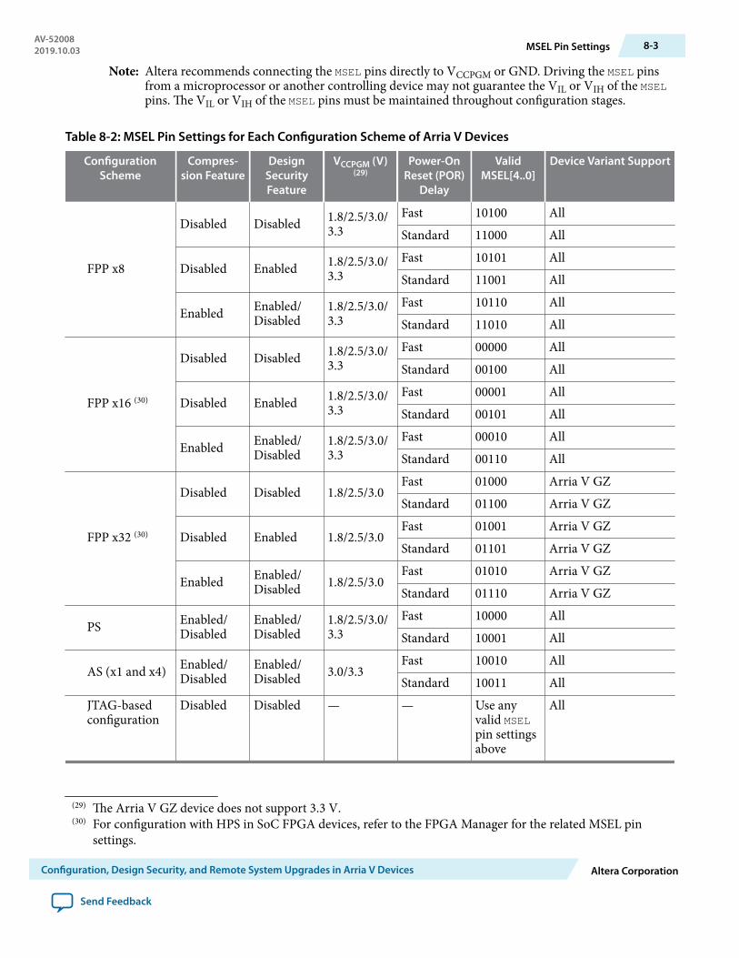
Note: Altera recommends connecting the MSEL pins directly to VCCPGM or GND. Driving the MSEL pinsfrom a microprocessor or another controlling device may not guarantee the VIL or VIH of the MSELpins. The VIL or VIH of the MSEL pins must be maintained throughout configuration stages.
Table 8-2: MSEL Pin Settings for Each Configuration Scheme of Arria V Devices
ConfigurationScheme
Compres‐sion Feature
DesignSecurityFeature
VCCPGM (V)(29)
Power-OnReset (POR)
Delay
ValidMSEL[4..0]
Device Variant Support
FPP x8
Disabled Disabled 1.8/2.5/3.0/3.3
Fast 10100 AllStandard 11000 All
Disabled Enabled 1.8/2.5/3.0/3.3
Fast 10101 AllStandard 11001 All
Enabled Enabled/Disabled
1.8/2.5/3.0/3.3
Fast 10110 AllStandard 11010 All
FPP x16 (30)
Disabled Disabled 1.8/2.5/3.0/3.3
Fast 00000 AllStandard 00100 All
Disabled Enabled 1.8/2.5/3.0/3.3
Fast 00001 AllStandard 00101 All
Enabled Enabled/Disabled
1.8/2.5/3.0/3.3
Fast 00010 AllStandard 00110 All
FPP x32 (30)
Disabled Disabled 1.8/2.5/3.0Fast 01000 Arria V GZStandard 01100 Arria V GZ
Disabled Enabled 1.8/2.5/3.0Fast 01001 Arria V GZStandard 01101 Arria V GZ
Enabled Enabled/Disabled 1.8/2.5/3.0
Fast 01010 Arria V GZStandard 01110 Arria V GZ
PS Enabled/Disabled
Enabled/Disabled
1.8/2.5/3.0/3.3
Fast 10000 AllStandard 10001 All
AS (x1 and x4) Enabled/Disabled
Enabled/Disabled 3.0/3.3
Fast 10010 AllStandard 10011 All
JTAG-basedconfiguration
Disabled Disabled — — Use anyvalid MSELpin settingsabove
All
(29) The Arria V GZ device does not support 3.3 V.(30) For configuration with HPS in SoC FPGA devices, refer to the FPGA Manager for the related MSEL pin
settings.
AV-520082019.10.03 MSEL Pin Settings 8-3
Configuration, Design Security, and Remote System Upgrades in Arria V Devices Altera Corporation
Send Feedback

Note: You must also select the configuration scheme in the Configuration page of the Device and PinOptions dialog box in the Intel Quartus Prime software. Based on your selection, the option bit inthe programming file is set accordingly.
Related Information
• FPGA ManagerProvides more information about the MSEL pin settings for configuration with hard processor system(HPS) in system on a chip (SoC) FPGA devices.
• Arria V GT and GX Device Family Pin Connection GuidelinesProvides more information about JTAG pins voltage-level connection.
• Arria V GZ Device Family Pin Connection GuidelinesProvides more information about JTAG pins voltage-level connection.
Configuration SequenceDescribes the configuration sequence and each configuration stage.
8-4 Configuration SequenceAV-52008
2019.10.03
Altera Corporation Configuration, Design Security, and Remote System Upgrades in Arria V Devices
Send Feedback
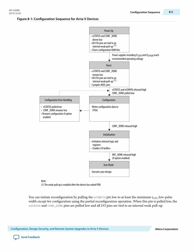
Figure 8-1: Configuration Sequence for Arria V Devices
nSTATUS and nCONFIG released highCONF_DONE pulled low
CONF_DONE released high
INIT_DONE released high(if option enabled)
Power Up
•
• All I/Os pins are tied to an internal weak pull-up (1)
• Clears configuration RAM bits
Reset
• nSTATUS and CONF_DONEremain low
• All I/Os pins are tied to an internal weak pull-up (1)
• Samples MSEL pins
Initialization
• Initializes internal logic and registers
• Enables I/O buffers
Configuration Error Handling
• • CONF_DONE remains low• Restarts configuration if option
enabled
User Mode
Executes your design
Configuration
Writes configuration data to FPGA
Power supplies including VCCPD and VCCPGM reachrecommended operating voltage
Note: (1) The weak-pull up is enabled after the device has exited POR.
nSTATUS and CONF_DONEdriven low
nSTATUS pulled low
You can initiate reconfiguration by pulling the nCONFIG pin low to at least the minimum tCFG low-pulsewidth except for configuration using the partial reconfiguration operation. When this pin is pulled low, thenSTATUS and CONF_DONE pins are pulled low and all I/O pins are tied to an internal weak pull-up.
AV-520082019.10.03 Configuration Sequence 8-5
Configuration, Design Security, and Remote System Upgrades in Arria V Devices Altera Corporation
Send Feedback

Power UpPower up all the power supplies that are monitored by the POR circuitry. All power supplies, includingVCCPGM and VCCPD, must ramp up from 0 V to the recommended operating voltage level within theramp-up time specification. Otherwise, hold the nCONFIG pin low until all the power supplies reach therecommended voltage level.
VCCPGM Pin
The configuration input buffers do not have to share power lines with the regular I/O buffers in Arria Vdevices.
The operating voltage for the configuration input pin is independent of the I/O banks power supply,VCCIO, during configuration. Therefore, Arria V devices do not require configuration voltage constraintson VCCIO.
VCCPD Pin
Use the VCCPD pin, a dedicated programming power supply, to power the I/O pre-drivers and JTAG I/Opins (TCK, TMS, TDI, and TDO).
The supported configuration voltages are 2.5, 3.0, and 3.3 V for all Arria V devices except for Arria V GZdevices. The supported configuration voltages for Arria V GZ devices are 2.5 and 3.0 V.
If VCCIO of the bank is set to 2.5 V or lower, VCCPD must be powered up at 2.5 V. If VCCIO is set greaterthan 2.5 V, VCCPD must be greater than VCCIO. For example, when VCCIO is set to 3.0 V, VCCPD must beset at 3.0 V or above. When VCCIO is set to 3.3 V, VCCPD must be set at 3.3 V.
Related Information
• Arria V Device DatasheetProvides more information about the ramp-up time specifications.
• Arria V GT and GX Device Family Pin Connection GuidelinesProvides more information about configuration pin connections.
• Arria V GZ Device Family Pin Connection GuidelinesProvides more information about configuration pin connections.
• Device Configuration Pins on page 8-11Provides more information about configuration pins.
• I/O Standards Voltage Levels in Arria V Devices on page 5-8Provides more information about typical power supplies for each supported I/O standards in Arria Vdevices.
ResetPOR delay is the time frame between the time when all the power supplies monitored by the POR circuitryreach the recommended operating voltage and when nSTATUS is released high and the Arria V device isready to begin configuration.
Set the POR delay using the MSEL pins.
The user I/O pins are tied to an internal weak pull-up until the device is configured.
Related Information
• MSEL Pin Settings on page 8-2
8-6 Power UpAV-52008
2019.10.03
Altera Corporation Configuration, Design Security, and Remote System Upgrades in Arria V Devices
Send Feedback
• Arria V Device DatasheetProvides more information about the POR delay specification.
ConfigurationFor more information about the DATA[] pins for each configuration scheme, refer to the appropriateconfiguration scheme.
Configuration Error HandlingTo restart configuration automatically, turn on the Auto-restart configuration after error option in theGeneral page of the Device and Pin Options dialog box in the Intel Quartus Prime software.
If you do not turn on this option, you can monitor the nSTATUS pin to detect errors. To restart configura‐tion, pull the nCONFIG pin low for at least the duration of tCFG.
Related InformationArria V Device DatasheetProvides more information about tSTATUS and tCFG timing parameters.
InitializationThe initialization clock source is from the internal oscillator, CLKUSR pin, or DCLK pin. By default, theinternal oscillator is the clock source for initialization. If you use the internal oscillator, the Arria V devicewill be provided with enough clock cycles for proper initialization.
Note: If you use the optional CLKUSR pin as the initialization clock source and the nCONFIG pin is pulledlow to restart configuration during device initialization, ensure that the CLKUSR or DCLK pincontinues toggling until the nSTATUS pin goes low and then goes high again.
The CLKUSR pin provides you with the flexibility to synchronize initialization of multiple devices or todelay initialization. Supplying a clock on the CLKUSR pin during initialization does not affect configuration.After the CONF_DONE pin goes high, the CLKUSR or DCLK pin is enabled after the time specified by tCD2CU.When this time period elapses, Arria V devices require a minimum number of clock cycles as specified byTinit to initialize properly and enter user mode as specified by the tCD2UMC parameter.
Related InformationArria V Device DatasheetProvides more information about tCD2CU, tinit, and tCD2UMC timing parameters, and initialization clocksource.
User ModeYou can enable the optional INIT_DONE pin to monitor the initialization stage. After the INIT_DONE pin ispulled high, initialization completes and your design starts executing. The user I/O pins will then functionas specified by your design.
AV-520082019.10.03 Configuration 8-7
Configuration, Design Security, and Remote System Upgrades in Arria V Devices Altera Corporation
Send Feedback

Configuration Timing Waveforms
FPP Configuration TimingFigure 8-2: FPP Configuration Timing Waveform when DCLK-to-DATA[] Ratio is 1
nCONFIG
nSTATUS (1)
CONF_DONE (2)
DCLK
DATA[15..0] (4)
User I/O
INIT_DONE (6)
Word 0 Word 1 Word 2 Word 3
tCD2UM
tCF2ST1
tCF2CD
tCFG
tCH tCL
tDH
tDSU
tCF2CK
tSTATUS
tCLKtCF2ST0
tST2CK
High-Z User Mode
(3)
User ModeWord n-2 Word n-1
(5)
Notes:(1) After power up, the FPGA holds nSTATUS low for the time of the POR delay.(2) After power up, before and during configuration, CONF_DONE is low.(3) Do not leave DCLK floating after configuration. DCLK is ignored after configuration is complete. It can toggle high or low if required.(4) For FPP x16, use DATA[15..0]. For FPP x8, use DATA[7..0]. DATA[15..5] are available as a user I/O pin after configuration. The state of this pin depends on the dual-purpose pin settings.(5) To ensure a successful configuration, send the entire configuration data to the FPGA. CONF_DONE is released high when the FPGA receives all the configuration data successfully. After CONF_DONE goes high, send two additional falling edges on DCLK to begin initialization and enter user mode.(6) After the option bit to enable the INIT_DONE pin is configured into the device, the INIT_DONE goes low.
8-8 Configuration Timing WaveformsAV-52008
2019.10.03
Altera Corporation Configuration, Design Security, and Remote System Upgrades in Arria V Devices
Send Feedback

Figure 8-3: FPP Configuration Timing Waveform when DCLK-to-DATA[] Ratio is >1
nCONFIG
nSTATUS (1)
CONF_DONE (2)
DCLK (4)
DATA[15..0] (6)
User I/O
INIT_DONE (7)
tCD2UM
tCF2ST1
tCF2CD
tCFG
tCF2CK
ttCF2ST0
tST2CK
High-Z User Mode
1 2 r 1 2 r 1 2
Word 0 Word 1 Word 3
1
tDSU tDH
STATUS
tDH
tCH
tCL
tCLK
Word (n-1)
(5)
(6)
(3)
User Mode
r
Notes:(1) After power up, the FPGA holds nSTATUS low for the time as specified by the POR delay.(2) After power up, before and during configuration, CONF_DONE is low.(3) Do not leave DCLK floating after configuration. DCLK is ignored after configuration is complete. It can toggle high or low if required.(4) “r” denotes the DCLK-to-DATA[] ratio. For the DCLK-to-DATA[] ratio based on the decompression and the design security feature enable settings, refer to the DCLK-to-DATA[] Ratio table.(5) If needed, pause DCLK by holding it low. When DCLK restarts, the external host must provide data on the DATA[15..0] pins prior to sending the first DCLK rising edge.(6) To ensure a successful configuration, send the entire configuration data to the FPGA. CONF_DONE is released high after the FPGA device receives all the configuration data successfully. After CONF_DONE goes high, send two additional falling edges on DCLK to begin initialization and enter user mode.(7) After the option bit to enable the INIT_DONE pin is configured into the device, the INIT_DONE goes low.
Related Information
• FPP Configuration Timing when DCLK-to-DATA[] = 1• FPP Configuration Timing when DCLK-to-DATA[] >1
AV-520082019.10.03 FPP Configuration Timing 8-9
Configuration, Design Security, and Remote System Upgrades in Arria V Devices Altera Corporation
Send Feedback
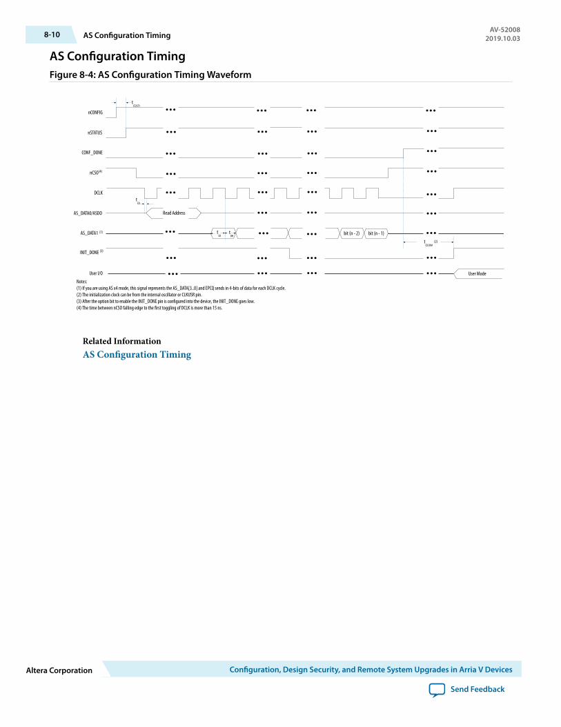
AS Configuration TimingFigure 8-4: AS Configuration Timing Waveform
Read Address
bit (n - 2) bit (n - 1)
tCD2UM
nSTATUS
nCONFIG
CONF_DONE
nCSO
DCLK
AS_DATA0/ASDO
AS_DATA1
INIT_DONE
User I/O User Mode
tCF2ST1
tDH
tCO
Notes:(1) If you are using AS x4 mode, this signal represents the AS_DATA[3..0] and EPCQ sends in 4-bits of data for each DCLK cycle.(2) The initialization clock can be from the internal oscillator or CLKUSR pin.(3) After the option bit to enable the INIT_DONE pin is configured into the device, the INIT_DONE goes low.(4) The time between nCSO falling edge to the first toggling of DCLK is more than 15 ns.
tSU
(3)
(1)
(4)
(2)
Related InformationAS Configuration Timing
8-10 AS Configuration TimingAV-52008
2019.10.03
Altera Corporation Configuration, Design Security, and Remote System Upgrades in Arria V Devices
Send Feedback
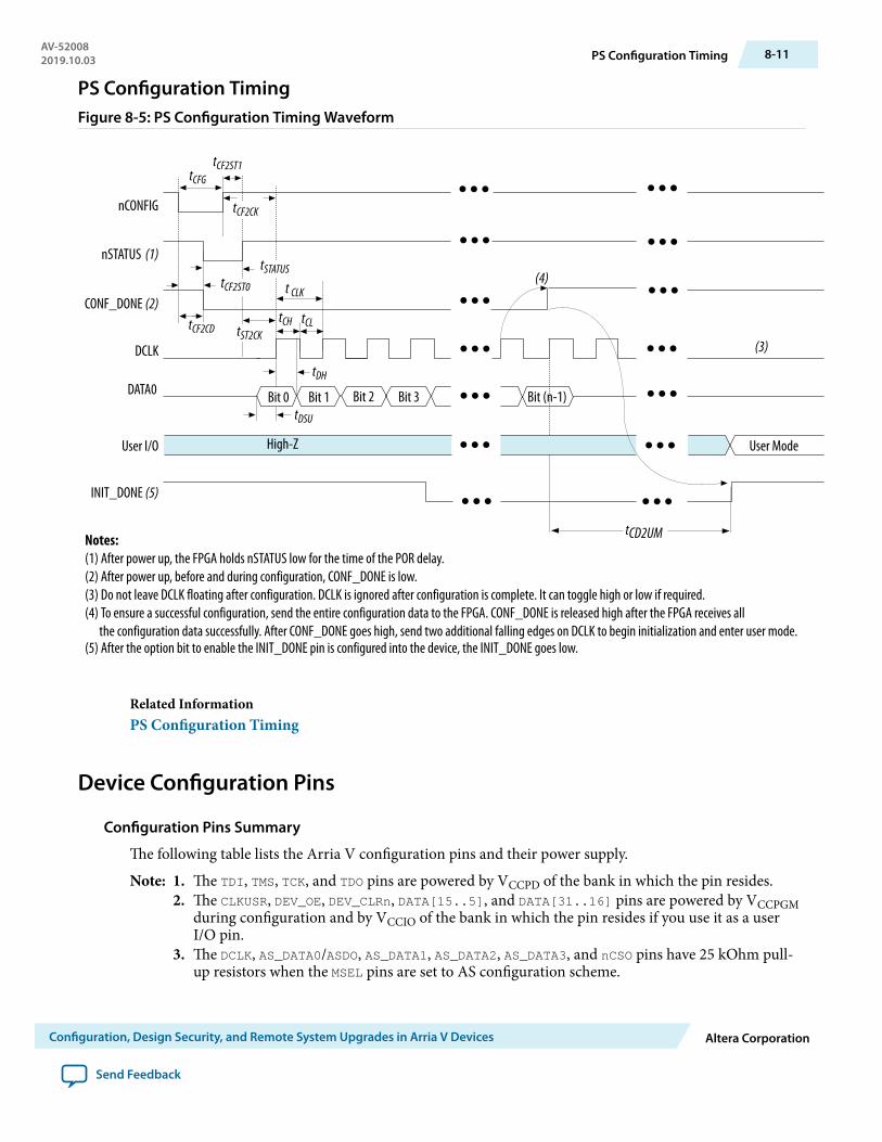
PS Configuration TimingFigure 8-5: PS Configuration Timing Waveform
nCONFIG
nSTATUS (1)
CONF_DONE (2)
DCLK
DATA0
User I/O
INIT_DONE (5)
Bit 0 Bit 1 Bit 2 Bit 3 Bit (n-1)
tCD2UM
tCF2ST1
tCF2CD
tCFG
tCH tCL
tDH
tDSU
tCF2CK
tSTATUS
t CLKtCF2ST0
tST2CK
High-Z User Mode
(4)
(3)
Notes:(1) After power up, the FPGA holds nSTATUS low for the time of the POR delay.(2) After power up, before and during configuration, CONF_DONE is low.(3) Do not leave DCLK floating after configuration. DCLK is ignored after configuration is complete. It can toggle high or low if required.(4) To ensure a successful configuration, send the entire configuration data to the FPGA. CONF_DONE is released high after the FPGA receives all the configuration data successfully. After CONF_DONE goes high, send two additional falling edges on DCLK to begin initialization and enter user mode.(5) After the option bit to enable the INIT_DONE pin is configured into the device, the INIT_DONE goes low.
Related InformationPS Configuration Timing
Device Configuration Pins
Configuration Pins Summary
The following table lists the Arria V configuration pins and their power supply.
Note: 1. The TDI, TMS, TCK, and TDO pins are powered by VCCPD of the bank in which the pin resides.2. The CLKUSR, DEV_OE, DEV_CLRn, DATA[15..5], and DATA[31..16] pins are powered by VCCPGM
during configuration and by VCCIO of the bank in which the pin resides if you use it as a userI/O pin.
3. The DCLK, AS_DATA0/ASDO, AS_DATA1, AS_DATA2, AS_DATA3, and nCSO pins have 25 kOhm pull-up resistors when the MSEL pins are set to AS configuration scheme.
AV-520082019.10.03 PS Configuration Timing 8-11
Configuration, Design Security, and Remote System Upgrades in Arria V Devices Altera Corporation
Send Feedback

Table 8-3: Configuration Pin Summary for Arria V Devices
Configuration Pin ConfigurationScheme
Input/Output User Mode Powered By
TDI JTAG Input — VCCPD
TMS JTAG Input — VCCPD
TCK JTAG Input — VCCPD
TDO JTAG Output — VCCPD
CLKUSR Allschemes
Input I/O VCCPGM/VCCIO (31)
CRC_ERROR Optional,allschemes
Output I/O Pull-up
CONF_DONE Allschemes
Bidirectional — VCCPGM/Pull-up
DCLK
FPP andPS
Input — VCCPGM
AS Output — VCCPGM
DEV_OE Optional,allschemes
Input I/O VCCPGM/VCCIO(31)
DEV_CLRn Optional,allschemes
I/O VCCPGM/VCCIO (31)
INIT_DONE Optional,allschemes
Output I/O Pull-up
MSEL[4..0] Allschemes
Input — VCCPGM
nSTATUS Allschemes
Bidirectional — VCCPGM/Pull-up
nCE Allschemes
Input — VCCPGM
nCEO Allschemes
Output I/O Pull-up
nCONFIG Allschemes
Input — VCCPGM
nIO_PULLUP(32) Allschemes
Input — VCCPGM
(31) This pin is powered by VCCPGM during configuration and powered by VCCIO of the bank in which the pinresides when you use this pin as a user I/O pin.
(32) These pins are applicable for Arria V GZ devices only.
8-12 Device Configuration PinsAV-52008
2019.10.03
Altera Corporation Configuration, Design Security, and Remote System Upgrades in Arria V Devices
Send Feedback

Configuration Pin ConfigurationScheme
Input/Output User Mode Powered By
DATA[15..5] FPP x8and x16
Input I/O VCCPGM/VCCIO (31)
DATA[31..16] (32) FPP x32 Input I/O VCCPGM/VCCIO(31)
DATA[4..0] (32) FPP x8,x16, andx32
Input I/O VCCPGM/VCCIO (31)
nCSO/DATA4 (33)AS Output — VCCPGM
FPP Input — VCCPGM
AS_DATA[3..1]/DATA[3..1] (33)
AS Bidirectional — VCCPGM
FPP Input — VCCPGM
AS_DATA0/DATA0/ASDO(33)
AS Bidirectional — VCCPGM
FPP andPS
Input — VCCPGM
AS_DATA0/ASDO(32) AS Bidirectional — VCCPGM
AS_DATA[3..1](32) AS Bidirectional — VCCPGM
PR_REQUEST PartialReconfiguration
Input I/O VCCPGM/VCCIO (31)
PR_READY PartialReconfiguration
Output I/O VCCPGM/VCCIO (31)
PR_ERROR PartialReconfiguration
Output I/O VCCPGM/VCCIO (31)
PR_DONE PartialReconfiguration
Output I/O VCCPGM/VCCIO (31)
CvP_CONFDONE CvP(PCIe)
Output I/O VCCPGM/VCCIO (31)
Related Information
• Arria V GT and GX Device Family Pin Connection GuidelinesProvides more information about each configuration pin.
• Arria V GZ Device Family Pin Connection GuidelinesProvides more information about each configuration pin.
(33) These pins are applicable for all Arria V devices except for Arria V GZ devices.
AV-520082019.10.03 Device Configuration Pins 8-13
Configuration, Design Security, and Remote System Upgrades in Arria V Devices Altera Corporation
Send Feedback

I/O Standards and Drive Strength for Configuration PinsIn configuration mode, the output drive strength is set as listed in the table below. Dual-function pinoutput drive strength is programmable if it is used as a regular I/O pin.
Table 8-4: I/O Standards and Drive Strength for Configuration Pins
The configuration pins listed support only fast slew rate and OCT is not enabled for these pins.Configuration Pin Type I/O Standard Drive Strength (mA)
nSTATUS Dedicated 3.0 V LVTTL 4CONF_DONE Dedicated 3.0 V LVTTL 4
CvP_CONFDONE Dual Function 3.0 V LVTTL 4DCLK Dedicated 3.0 V LVTTL 12TDO Dedicated 3.0 V LVTTL 12
AS_DATA0/ASDO Dedicated 3.0 V LVTTL 8AS_DATA1 Dedicated 3.0 V LVTTL 8AS_DATA2 Dedicated 3.0 V LVTTL 8AS_DATA3 Dedicated 3.0 V LVTTL 8INIT_DONE Dual Function 3.0 V LVTTL 8CRC_ERROR Dual Function 3.0 V LVTTL 8
nCSO Dedicated 3.0 V LVTTL 8
Configuration Pin Options in the Intel Quartus Prime SoftwareThe following table lists the dual-purpose configuration pins available in the Device and Pin Optionsdialog box in the Intel Quartus Prime software.
Table 8-5: Configuration Pin Options
Configuration Pin Category Page Option
CLKUSR General Enable user-supplied start-up clock(CLKUSR)
DEV_CLRn General Enable device-wide reset(DEV_CLRn)
DEV_OE General Enable device-wide output enable(DEV_OE)
INIT_DONE General Enable INIT_DONE outputnCEO General Enable nCEO pin
8-14 I/O Standards and Drive Strength for Configuration PinsAV-52008
2019.10.03
Altera Corporation Configuration, Design Security, and Remote System Upgrades in Arria V Devices
Send Feedback
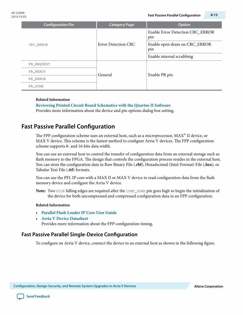
Configuration Pin Category Page Option
CRC_ERROR Error Detection CRC
Enable Error Detection CRC_ERRORpinEnable open drain on CRC_ERRORpinEnable internal scrubbing
PR_REQUEST
General Enable PR pinPR_READY
PR_ERROR
PR_DONE
Related InformationReviewing Printed Circuit Board Schematics with the Quartus II SoftwareProvides more information about the device and pin options dialog box setting.
Fast Passive Parallel ConfigurationThe FPP configuration scheme uses an external host, such as a microprocessor, MAX® II device, orMAX V device. This scheme is the fastest method to configure Arria V devices. The FPP configurationscheme supports 8- and 16-bits data width.
You can use an external host to control the transfer of configuration data from an external storage such asflash memory to the FPGA. The design that controls the configuration process resides in the external host.You can store the configuration data in Raw Binary File (.rbf), Hexadecimal (Intel-Format) File (.hex), orTabular Text File (.ttf) formats.
You can use the PFL IP core with a MAX II or MAX V device to read configuration data from the flashmemory device and configure the Arria V device.
Note: Two DCLK falling edges are required after the CONF_DONE pin goes high to begin the initialization ofthe device for both uncompressed and compressed configuration data in an FPP configuration.
Related Information
• Parallel Flash Loader IP Core User Guide• Arria V Device Datasheet
Provides more information about the FPP configuration timing.
Fast Passive Parallel Single-Device ConfigurationTo configure an Arria V device, connect the device to an external host as shown in the following figure.
AV-520082019.10.03 Fast Passive Parallel Configuration 8-15
Configuration, Design Security, and Remote System Upgrades in Arria V Devices Altera Corporation
Send Feedback
Figure 8-6: Single Device FPP Configuration Using an External Host
CONF_DONEnSTATUSnCE
DATA[]nCONFIG
FPGA Device
Memory
ADDR DATA[7..0]
GND
MSEL[4..0]
DCLK
nCEO N.C.
10 kΩ 10 kΩ
VCCPGM VCCPGM
Connect the resistor to a supply that provides an acceptable input signal for the FPGA device. VCCPGM must be high enough to meet the VIH specification of the I/O on the device and the external host. Altera recommends powering up all configuration system I/Os with VCCPGM.
External Host(MAX II Device,
MAX V Device, or Microprocessor)
You can leave the nCEO pin unconnected or use it as a user I/O pin when it does not feed another device’s nCE pin.
For more information, refer to the MSEL pin settings.
Fast Passive Parallel Multi-Device ConfigurationYou can configure multiple Arria V devices that are connected in a chain.
Pin Connections and Guidelines
Observe the following pin connections and guidelines for this configuration setup:
• Tie the following pins of all devices in the chain together:
• nCONFIG
• nSTATUS
• DCLK
• DATA[]
• CONF_DONE
By tying the CONF_DONE and nSTATUS pins together, the devices initialize and enter user mode at thesame time. If any device in the chain detects an error, configuration stops for the entire chain and youmust reconfigure all the devices. For example, if the first device in the chain flags an error on thenSTATUS pin, it resets the chain by pulling its nSTATUS pin low.
• Ensure that DCLK and DATA[] are buffered for every fourth device to prevent signal integrity and clockskew problems.
• All devices in the chain must use the same data width.• If you are configuring the devices in the chain using the same configuration data, the devices must be
of the same package and density.
Using Multiple Configuration Data
To configure multiple Arria V devices in a chain using multiple configuration data, connect the devices toan external host as shown in the following figure.
8-16 Fast Passive Parallel Multi-Device ConfigurationAV-52008
2019.10.03
Altera Corporation Configuration, Design Security, and Remote System Upgrades in Arria V Devices
Send Feedback

Figure 8-7: Multiple Device FPP Configuration Using an External Host When Both Devices Receive aDifferent Set of Configuration Data
Connect the resistor to a supply that provides an acceptable input signal for the FPGA device. VCCPGM must be high enough to meet the VIH specification of the I/O on the device and the external host. Altera recommends powering up all configuration system I/Os with VCCPGM.
CONF_DONEnSTATUSnCE
nCONFIG
Memory
ADDR DATA[7..0]
GND
10 kΩ10 kΩ
DCLK
nCEO
CONF_DONEnSTATUSnCE
nCONFIGDCLK
nCEO
VCCPGM VCCPGM
DATA[]
MSEL[4..0]
DATA[]
MSEL[4..0]
Buffers
FPGA Device Master FPGA Device Slave
N.C.
10 kΩ
VCCPGM
You can leave the nCEO pin unconnected or use it as a user I/O pin when it does not feed another device’s nCE pin.
For more information, refer to the MSEL pin settings.
Connect the repeater buffers between the FPGA master and slave device for DATA[] and DCLK for every fourth device.
External Host(MAX II Device,
MAX V Device, or Microprocessor)
When a device completes configuration, its nCEO pin is released low to activate the nCE pin of the nextdevice in the chain. Configuration automatically begins for the second device in one clock cycle.
Using One Configuration Data
To configure multiple Arria V devices in a chain using one configuration data, connect the devices to anexternal host as shown in the following figure.
AV-520082019.10.03 Using One Configuration Data 8-17
Configuration, Design Security, and Remote System Upgrades in Arria V Devices Altera Corporation
Send Feedback

Figure 8-8: Multiple Device FPP Configuration Using an External Host When Both Devices Receive theSame Data
nCONFIG
Memory
ADDR DATA[7..0]
DCLK
nCEO N.C.
nCONFIGDCLK
nCEO N.C.
MSEL[4..0] MSEL[4..0]
VCCPGM VCCPGM
10 kΩ 10 kΩ
GND GND
CONF_DONE CONF_DONEnSTATUS nSTATUSnCE nCE
DATA[] DATA[]
Buffers
FPGA Device Master FPGA Device Slave
Connect the resistor to a supply that provides an acceptable input signal for the FPGA device. VCCPGM must be high enough to meet the VIH specification of the I/O on the device and the external host. Altera recommends powering up all configuration system I/Os with VCCPGM.
Connect the repeater buffers between the FPGA master and slave device for DATA[] and DCLK for every fourth device.
You can leave the nCEO pin unconnected or use it as a user I/O pin when it does not feed another device’s nCE pin.
For more information, refer to the MSEL pin settings.
External Host(MAX II Device,
MAX V Device, orMicroprocessor)
The nCE pins of the device in the chain are connected to GND, allowing configuration for these devices tobegin and end at the same time.
Transmitting Configuration DataThis section describes how to transmit configuration data when you are using .rbf file for FPP x8, x16, andx32 configuration schemes. The configuration data in the .rbf file is little endian.
For example, if the .rbf file contains the byte sequence 02 1B EE 01, refer to the following tables for detailson how this data is transmitted in the FPP x8, x16, and x32 configuration schemes.
Table 8-6: Transmitting Configuration Data for FPP x8 Configuration Scheme
In FPP x8 configuration scheme, the LSB of a byte is BIT0, and the MSB is BIT7.BYTE0 = 02 BYTE1 = 1B BYTE2 = EE BYTE3 = 01
D[7..0] D[7..0] D[7..0] D[7..0]
0000 0010 0001 1011 1110 1110 0000 0001
Table 8-7: Transmitting Configuration Data for FPP x16 Configuration Scheme
In FPP x16 configuration scheme, the first byte in the file is the LSB of the configuration word, and thesecond byte in the file is the MSB of the configuration word.
8-18 Transmitting Configuration DataAV-52008
2019.10.03
Altera Corporation Configuration, Design Security, and Remote System Upgrades in Arria V Devices
Send Feedback
WORD0 = 1B02 WORD1 = 01EE
LSB: BYTE0 = 02 MSB: BYTE1 = 1B LSB: BYTE2 = EE MSB: BYTE3 = 01
D[7..0] D[15..8] D[7..0] D[15..8]
0000 0010 0001 1011 1110 1110 0000 0001
Table 8-8: Transmitting Configuration Data for FPP x32 Configuration Scheme
In FPP x32 configuration scheme, the first byte in the file is the LSB of the configuration double word, andthe fourth byte is the MSB.
Double Word = 01EE1B02
LSB: BYTE0 = 02 BYTE1 = 1B BYTE2 = EE MSB: BYTE3 = 01
D[7..0] D[15..8] D[23..16] D[31..24]
0000 0010 0001 1011 1110 1110 0000 0001
Ensure that you do not swap the upper bits or bytes with the lower bits or bytes when performing the FPPconfiguration. Sending incorrect configuration data during the configuration process may causeunexpected behavior on the CONF_DONE signal.
Active Serial ConfigurationThe AS configuration scheme supports AS x1 (1-bit data width) and AS x4 (4-bit data width) modes. TheAS x4 mode provides four times faster configuration time than the AS x1 mode. In the AS configurationscheme, the Arria V device controls the configuration interface.
In the AS configuration process, after power-up, the Arria V device drives the DCLK pin with the default12.5 MHz internal oscillator to read the configuration bitstream from the serial flash. The devicedetermines the configuration options such as clock source, DCLK frequency, ASx1, or ASx4 by reading theoption bits, located from 0x80 to 0x127, at the start of the programming file stored in the serial flash.
After the option bit is decoded by the Arria V configuration control block, the AS configuration continueswith the design option by reading the rest of the programming file from the serial flash until CONF_DONEpin asserts high and eventually enters user mode. When any interruption (such as data corruption) occursin the middle of the AS Configuration, the nSTATUS pin will assert low to indicate configuration error, anddeassert high to restart the configuration process. If there is no image in the serial flash or if the image iscorrupted, you will observe the nSTATUS will pulse low repeatedly as the control block tries to configureitself forever, until the configuration is successful.
Related InformationArria V Device DatasheetProvides more information about the AS configuration timing.
AV-520082019.10.03 Active Serial Configuration 8-19
Configuration, Design Security, and Remote System Upgrades in Arria V Devices Altera Corporation
Send Feedback
DATA Clock (DCLK)Arria V devices generate the serial clock, DCLK, that provides timing to the serial interface. In the ASconfiguration scheme, Arria V devices drive control signals on the falling edge of DCLK and latch theconfiguration data on the following falling edge of this clock pin.
The maximum DCLK frequency supported by the AS configuration scheme is 100 MHz except for the ASmulti-device configuration scheme. You can source DCLK using CLKUSR or the internal oscillator. If you usethe internal oscillator, you can choose a 12.5, 25, 50, or 100 MHz clock under the Device and Pin Optionsdialog box, in the Configuration page of the Intel Quartus Prime software.
After power-up, DCLK is driven by a 12.5 MHz internal oscillator by default. The Arria V device determinesthe clock source and frequency to use by reading the option bit in the programming file.
Related InformationArria V Device DatasheetProvides more information about the DCLK frequency specification in the AS configuration scheme.
Active Serial Single-Device ConfigurationTo configure an Arria V device, connect the device to a serial configuration (EPCS) device or quad-serialconfiguration (EPCQ) device, as shown in the following figures.
Figure 8-9: Single Device AS x1 Mode Configuration
DATADCLK
nCSASDI
AS_DATA1DCLKnCSO ASDO
EPCS or EPCQ Device FPGA Device
10 kΩ10 kΩ10 kΩ
VCCPGM
GND
nCEO
nCE
nSTATUS
nCONFIGCONF_DONE N.C.
MSEL[4..0]
CLKUSR
VCCPGM VCCPGM
Connect the pull-up resistors to VCCPGM at 3.0- or 3.3-V power supply.
For more information, refer to the MSEL pin settings.
Use the CLKUSR pin to supply the external clock source to drive DCLK during configuration.
8-20 DATA Clock (DCLK)AV-52008
2019.10.03
Altera Corporation Configuration, Design Security, and Remote System Upgrades in Arria V Devices
Send Feedback
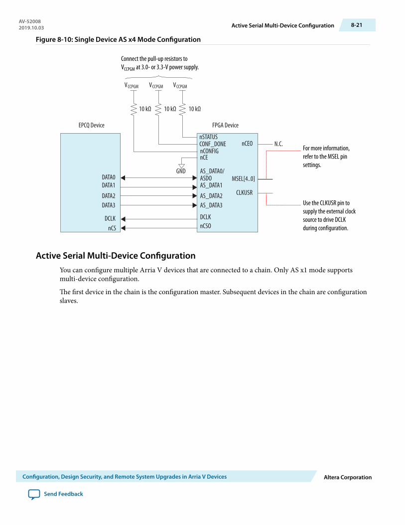
Figure 8-10: Single Device AS x4 Mode Configuration
AS_DATA0/ASDOAS_DATA1
AS_DATA2AS_DATA3
DCLKnCSO
EPCQ Device FPGA Device
10 kΩ10 kΩ10 kΩ
VCCPGM
GND
nCEO
nCE
nSTATUS
nCONFIGCONF_DONE N.C.
MSEL[4..0]
CLKUSR
VCCPGM VCCPGM
DATA0DATA1
DATA2DATA3
DCLKnCS
Connect the pull-up resistors to VCCPGM at 3.0- or 3.3-V power supply.
For more information, refer to the MSEL pin settings.
Use the CLKUSR pin to supply the external clock source to drive DCLK during configuration.
Active Serial Multi-Device ConfigurationYou can configure multiple Arria V devices that are connected to a chain. Only AS x1 mode supportsmulti-device configuration.
The first device in the chain is the configuration master. Subsequent devices in the chain are configurationslaves.
AV-520082019.10.03 Active Serial Multi-Device Configuration 8-21
Configuration, Design Security, and Remote System Upgrades in Arria V Devices Altera Corporation
Send Feedback
Pin Connections and Guidelines
Observe the following pin connections and guidelines for this configuration setup:
• Hardwire the MSEL pins of the first device in the chain to select the AS configuration scheme. Forsubsequent devices in the chain, hardwire their MSEL pins to select the PS configuration scheme. Anyother Altera® devices that support the PS configuration can also be part of the chain as a configurationslave.
• Tie the following pins of all devices in the chain together:
• nCONFIG
• nSTATUS
• DCLK
• DATA[]
• CONF_DONE
By tying the CONF_DONE, nSTATUS, and nCONFIG pins together, the devices initialize and enter usermode at the same time. If any device in the chain detects an error, configuration stops for the entirechain and you must reconfigure all the devices. For example, if the first device in the chain flags anerror on the nSTATUS pin, it resets the chain by pulling its nSTATUS pin low.
• Ensure that DCLK and DATA[] are buffered every fourth device to prevent signal integrity and clockskew problems.
Using Multiple Configuration Data
To configure multiple Arria V devices in a chain using multiple configuration data, connect the devices toan EPCS or EPCQ device, as shown in the following figure.
8-22 Pin Connections and GuidelinesAV-52008
2019.10.03
Altera Corporation Configuration, Design Security, and Remote System Upgrades in Arria V Devices
Send Feedback
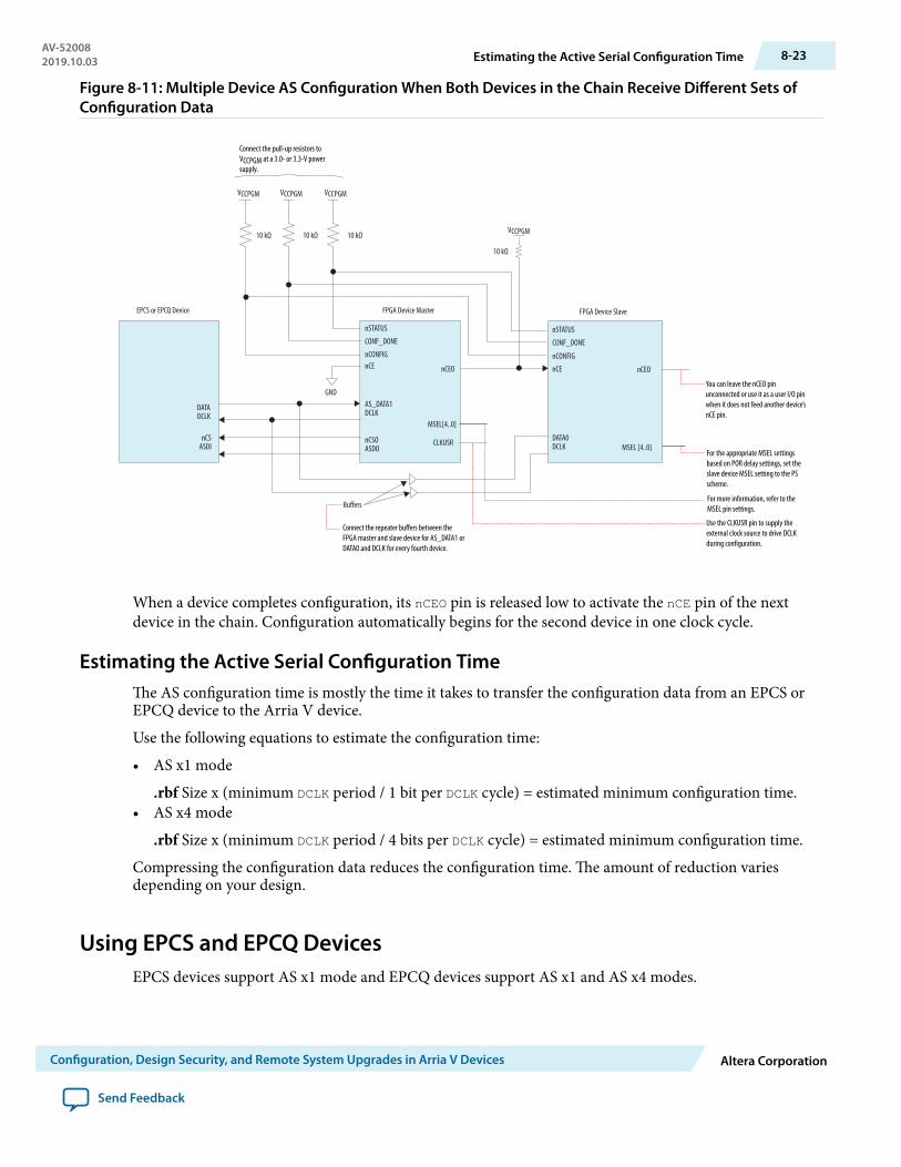
Figure 8-11: Multiple Device AS Configuration When Both Devices in the Chain Receive Different Sets ofConfiguration Data
DATADCLK
nCSASDI
EPCS or EPCQ Device FPGA Device Master FPGA Device Slave
GND
nCE nCEO
nSTATUS
CONF_DONE
DATA0DCLK
nCEO
nSTATUS
CONF_DONE
10 kΩ
nCONFIG nCONFIG
nCE
Buffers
MSEL [4..0]
AS_DATA1DCLK
nCSOASDO
MSEL[4..0]
CLKUSR
10 kΩ 10 kΩ
10 kΩ
Connect the pull-up resistors toVCCPGM at a 3.0- or 3.3-V powersupply.
VCCPGM
You can leave the nCEO pin unconnected or use it as a user I/O pin when it does not feed another device’s nCE pin.
For the appropriate MSEL settings based on POR delay settings, set the slave device MSEL setting to the PS scheme.
For more information, refer to the MSEL pin settings.
Use the CLKUSR pin to supply the external clock source to drive DCLK during configuration.
Connect the repeater buffers between the FPGA master and slave device for AS_DATA1 or DATA0 and DCLK for every fourth device.
VCCPGM VCCPGM VCCPGM
When a device completes configuration, its nCEO pin is released low to activate the nCE pin of the nextdevice in the chain. Configuration automatically begins for the second device in one clock cycle.
Estimating the Active Serial Configuration TimeThe AS configuration time is mostly the time it takes to transfer the configuration data from an EPCS orEPCQ device to the Arria V device.
Use the following equations to estimate the configuration time:
• AS x1 mode
.rbf Size x (minimum DCLK period / 1 bit per DCLK cycle) = estimated minimum configuration time.• AS x4 mode
.rbf Size x (minimum DCLK period / 4 bits per DCLK cycle) = estimated minimum configuration time.
Compressing the configuration data reduces the configuration time. The amount of reduction variesdepending on your design.
Using EPCS and EPCQ DevicesEPCS devices support AS x1 mode and EPCQ devices support AS x1 and AS x4 modes.
AV-520082019.10.03 Estimating the Active Serial Configuration Time 8-23
Configuration, Design Security, and Remote System Upgrades in Arria V Devices Altera Corporation
Send Feedback
Related Information
• Serial Configuration (EPCS) Devices Datasheet• Quad-Serial Configuration (EPCQ) Devices Datasheet
Controlling EPCS and EPCQ DevicesDuring configuration, Arria V devices enable the EPCS or EPCQ device by driving its nCSO output pinlow, which connects to the chip select (nCS) pin of the EPCS or EPCQ device. Arria V devices use the DCLKand ASDO pins to send operation commands and read address signals to the EPCS or EPCQ device. TheEPCS or EPCQ device provides data on its serial data output (DATA[]) pin, which connects to theAS_DATA[] input of the Arria V devices.
Note: If you wish to gain control of the EPCS pins, hold the nCONFIG pin low and pull the nCE pin high.This causes the device to reset and tri-state the AS configuration pins.
Trace Length and Loading GuidelineThe maximum trace length and loading apply to both single- and multi-device AS configuration setups aslisted in the following table. The trace length is the length from the Arria V device to the EPCS or EPCQdevice.
Table 8-9: Maximum Trace Length and Loading Guideline for AS x1 and x4 Configurations for Arria VDevices
Arria V Device AS PinsMaximum Board Trace Length (Inches)
Maximum Board Load (pF)12.5/ 25/ 50 MHz 100 MHz
DCLK 10 6 5DATA[3..0] 10 6 10nCSO 10 6 10
Programming EPCS and EPCQ DevicesYou can program EPCS and EPCQ devices in-system using a USB-Blaster™, EthernetBlaster,EthernetBlaster II, or ByteBlaster™ II download cable. Alternatively, you can program the EPCS or EPCQusing a microprocessor with the SRunner software driver.
In-system programming (ISP) offers you the option to program the EPCS or EPCQ either using an ASprogramming interface or a JTAG interface. Using the AS programming interface, the configuration datais programmed into the EPCS by the Intel Quartus Prime software or any supported third-party software.Using the JTAG interface, an Altera IP called the serial flash loader (SFL) must be downloaded into theArria V device to form a bridge between the JTAG interface and the EPCS or EPCQ. This allows the EPCSor EPCQ to be programmed directly using the JTAG interface.
Related Information
• AN 370: Using the Serial FlashLoader with the Quartus II Software• AN 418: SRunner: An Embedded Solution for Serial Configuration Device Programming
8-24 Controlling EPCS and EPCQ DevicesAV-52008
2019.10.03
Altera Corporation Configuration, Design Security, and Remote System Upgrades in Arria V Devices
Send Feedback
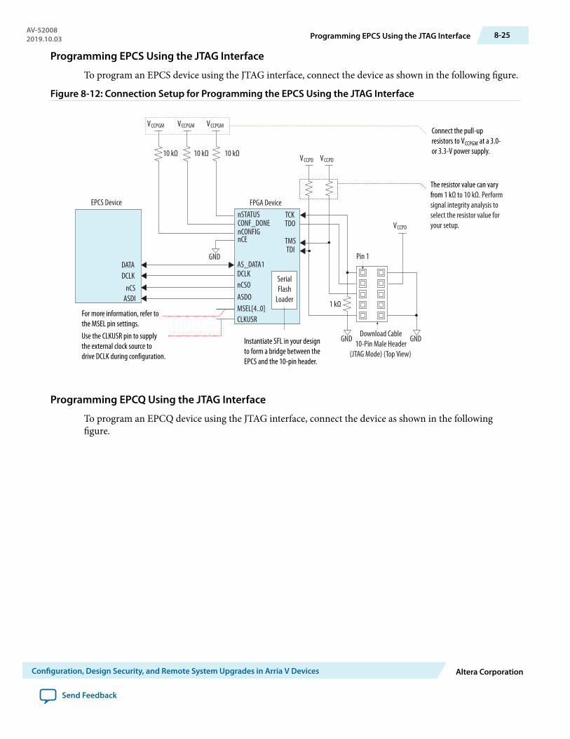
Programming EPCS Using the JTAG Interface
To program an EPCS device using the JTAG interface, connect the device as shown in the following figure.
Figure 8-12: Connection Setup for Programming the EPCS Using the JTAG Interface
DATADCLK
nCSASDI
FPGA Device
1 kΩ
GND
GND
nCE
TCKTDO
TMSTDI
nSTATUSCONF_DONE
10 kΩ
nCONFIG
AS_DATA1DCLKnCSOASDOMSEL[4..0]CLKUSR
GND
VCCPGM
VCCPD VCCPD
Pin 1
EPCS Device
10 kΩ 10 kΩ
VCCPGM VCCPGM
VCCPD
Connect the pull-up resistors to VCCPGM at a 3.0- or 3.3-V power supply.
The resistor value can vary from 1 kΩ to 10 kΩ. Perform signal integrity analysis to select the resistor value for your setup.
Download Cable10-Pin Male Header
(JTAG Mode) (Top View)
Instantiate SFL in your design to form a bridge between the EPCS and the 10-pin header.
For more information, refer to the MSEL pin settings.Use the CLKUSR pin to supply the external clock source to drive DCLK during configuration.
Serial Flash
Loader
Programming EPCQ Using the JTAG Interface
To program an EPCQ device using the JTAG interface, connect the device as shown in the followingfigure.
AV-520082019.10.03 Programming EPCS Using the JTAG Interface 8-25
Configuration, Design Security, and Remote System Upgrades in Arria V Devices Altera Corporation
Send Feedback

Figure 8-13: Connection Setup for Programming the EPCQ Using the JTAG Interface
DATA0DATA1DATA2DATA3
DCLKnCS
FPGA Device
1 kΩ
GND
nCE
TCKTDO
TMSTDI
MSEL[4..0]
nSTATUSCONF_DONEnCONFIG
AS_DATA0/ASDOAS_DATA1AS_DATA2AS_DATA3DCLKnCSO
CLKUSR
Pin 1
EPCQ Device
10 kΩ 10 kΩ 10 kΩ
GND GND
Connect the pull-up resistors to VCCPGM at a 3.0- or 3.3-V power supply.
The resistor value can vary from 1 kΩ to 10 kΩ. Perform signal integrity analysis to select the resistor value for your setup.
Download Cable10-Pin Male Header
(JTAG Mode) (Top View)
For more information, refer to the MSEL pin settings.
Use the CLKUSR pin to supply the external clock source to drive DCLK during configuration.
Instantiate SFL in your design to form a bridge between the EPCQ and the 10-pin header.
VCCPD
VCCPD
VCCPD
VCCPGMVCCPGM VCCPGM
Serial Flash
Loader
Programming EPCS Using the Active Serial Interface
To program an EPCS device using the AS interface, connect the device as shown in the following figure.
8-26 Programming EPCS Using the Active Serial InterfaceAV-52008
2019.10.03
Altera Corporation Configuration, Design Security, and Remote System Upgrades in Arria V Devices
Send Feedback
Figure 8-14: Connection Setup for Programming the EPCS Using the AS Interface
DATADCLK
nCSASDI
AS_DATA1DCLKnCSO
nCE
nCONFIGnSTATUS nCEOCONF_DONE
ASDO
10 kΩ
10 kΩ
10 kΩ 10 kΩ
FPGA Device
EPCS Device
Pin 1
N.C.
MSEL[4..0]CLKUSR
VCCPGM
GND
VCCPGMVCCPGM
VCCPGM
Connect the pull-up resistors to VCCPGM at a 3.0- or 3.3-V power supply.
For more information, refer to the MSEL pin settings.
Use the CLKUSR pin to supply the external clock source to drive DCLK during configuration.
Power up the USB-Blaster, ByteBlaster II, EthernetBlaster, or EthernetBlaster II cable’s VCC(TRGT) to VCCPGM.
USB-Blaster or ByteBlaster II (AS Mode)
10-Pin Male Header
Programming EPCQ Using the Active Serial Interface
To program an EPCQ device using the AS interface, connect the device as shown in the following figure.
AV-520082019.10.03 Programming EPCQ Using the Active Serial Interface 8-27
Configuration, Design Security, and Remote System Upgrades in Arria V Devices Altera Corporation
Send Feedback

Figure 8-15: Connection Setup for Programming the EPCQ Using the AS Interface
Using the AS header, the programmer serially transmits the operation commands and configuration bitsto the EPCQ on DATA0. This is equivalent to the programming operation for the EPCS.
DATA0DATA1
DATA3DCLK
nCS
DATA2
FPGA Device
AS_DATA0/ASDOAS_DATA1AS_DATA2AS_DATA3DCLKnCSO
EPCQ Device
nCE
MSEL[4..0]
nCONFIGnSTATUS nCEOCONF_DONE
10 kΩ10 kΩ 10 kΩ
10 kΩ
Pin 1
N.C.
CLKUSR
VCCPGM
VCCPGM
VCCPGMVCCPGM
GND
Connect the pull-up resistors to VCCPGM at a 3.0- or 3.3-V power supply.
For more information, refer to the MSEL pin settings.
Use the CLKUSR pin to supply the external clock source to drive DCLK during configuration.
Power up the USB-Blaster, ByteBlaster II, EthernetBlaster, or EthernetBlaster II cable’s V CC(TRGT) to VCCPGM.
USB-Blaster or ByteBlaster II (AS Mode)
10-Pin Male Header
When programming the EPCS and EPCQ devices, the download cable disables access to the AS interfaceby driving the nCE pin high. The nCONFIG line is also pulled low to hold the Arria V device in the resetstage. After programming completes, the download cable releases nCE and nCONFIG, allowing thepull-down and pull-up resistors to drive the pin to GND and VCCPGM, respectively.
During the EPCQ programming using the download cable, DATA0 transfers the programming data,operation command, and address information from the download cable into the EPCQ. During the EPCQverification using the download cable, DATA1 transfers the programming data back to the download cable.
Passive Serial ConfigurationThe PS configuration scheme uses an external host. You can use a microprocessor, MAX II device, MAX Vdevice, or a host PC as the external host.
8-28 Passive Serial ConfigurationAV-52008
2019.10.03
Altera Corporation Configuration, Design Security, and Remote System Upgrades in Arria V Devices
Send Feedback

You can use an external host to control the transfer of configuration data from an external storage such asflash memory to the FPGA. The design that controls the configuration process resides in the external host.
You can store the configuration data in Programmer Object File (.pof), .rbf, .hex, or .ttf. If you are usingconfiguration data in .rbf, .hex, or .ttf, send the LSB of each data byte first. For example, if the .rbfcontains the byte sequence 02 1B EE 01 FA, the serial data transmitted to the device must be 0100-00001101-1000 0111-0111 1000-0000 0101-1111.
You can use the PFL IP core with a MAX II or MAX V device to read configuration data from the flashmemory device and configure the Arria V device.
For a PC host, connect the PC to the device using a download cable such as the Altera USB-Blaster USBport, ByteBlaster II parallel port, EthernetBlaster, and EthernetBlaster II download cables.
The configuration data is shifted serially into the DATA0 pin of the device.
If you are using the Intel Quartus Prime programmer and the CLKUSR pin is enabled, you do not need toprovide a clock source for the pin to initialize your device.
Related Information
• Parallel Flash Loader IP Core User Guide• Arria V Device Datasheet
Provides more information about the PS configuration timing.
Passive Serial Single-Device Configuration Using an External HostTo configure an Arria V device, connect the device to an external host, as shown in the following figure.
Figure 8-16: Single Device PS Configuration Using an External Host
CONF_DONEnSTATUSnCE
DATA0nCONFIG
FPGA Device
Memory
ADDR
GND
10 kΩ
DCLK
nCEO N.C.
MSEL[4..0]
DATA010 kΩ
VCCPGM VCCPGM
Connect the resistor to a supply that provides an acceptable input signal for the FPGA device. VCCPGM must be high enough to meet the VIH specification of the I/O on the device and the external host. Altera recommends powering up all configuration system I/Os with VCCPGM.
You can leave the nCEO pin unconnected or use it as a user I/O pin when it does not feed another device’s nCE pin.
For more information, refer to the MSEL pin settings.
External Host(MAX II Device,
MAX V Device, orMicroprocessor)
Passive Serial Single-Device Configuration Using an Altera Download CableTo configure an Arria V device, connect the device to a download cable, as shown in the following figure.
AV-520082019.10.03 Passive Serial Single-Device Configuration Using an External Host 8-29
Configuration, Design Security, and Remote System Upgrades in Arria V Devices Altera Corporation
Send Feedback

Figure 8-17: Single Device PS Configuration Using an Altera Download Cable
VCCPGM VCCPGM VCCPGM VCCPGM VCCPGM
VCCIO
VIO
FPGA Device
DCLK
nCONFIG
CONF_DONE
ShieldGND
10 kΩ
nSTATUS
DATA0 Pin 1
nCE
GND
GND
nCEO N.C.
MSEL[4..0]
10 kΩ 10 kΩ 10 kΩ 10 kΩ
You only need the pull-up resistors on DATA0 and DCLK if the download cable is the only configuration scheme used on your board. This ensures that DATA0 and DCLK are not left floating after configuration. For example, if you are also using a MAX II device, MAX V device, or microprocessor, you do not need the pull-up resistors on DATA0 and DCLK.
For more information, refer to the MSEL pin settings.
In the USB-Blaster and ByteBlaster II cables, this pin is connected to nCE when you use it for AS programming. Otherwise, this pin is a no connect.
Connect the pull-up resistor to the same supply voltage (VCCIO) as the USB-Blaster, ByteBlaster II, EthernetBlaster, or EthernetBlaster II cable.
Download Cable10-Pin Male Header
(PS Mode)
Passive Serial Multi-Device ConfigurationYou can configure multiple Arria V devices that are connected in a chain.
8-30 Passive Serial Multi-Device ConfigurationAV-52008
2019.10.03
Altera Corporation Configuration, Design Security, and Remote System Upgrades in Arria V Devices
Send Feedback

Pin Connections and Guidelines
Observe the following pin connections and guidelines for this configuration setup:
• Tie the following pins of all devices in the chain together:
• nCONFIG
• nSTATUS
• DCLK
• DATA0
• CONF_DONE
By tying the CONF_DONE and nSTATUS pins together, the devices initialize and enter user mode at thesame time. If any device in the chain detects an error, configuration stops for the entire chain and youmust reconfigure all the devices. For example, if the first device in the chain flags an error on thenSTATUS pin, it resets the chain by pulling its nSTATUS pin low.
• If you are configuring the devices in the chain using the same configuration data, the devices must beof the same package and density.
Using Multiple Configuration Data
To configure multiple Arria V devices in a chain using multiple configuration data, connect the devices tothe external host as shown in the following figure.
Figure 8-18: Multiple Device PS Configuration when Both Devices Receive Different Sets of ConfigurationData
CONF_DONEnSTATUSnCE
DATA0nCONFIG
FPGA Device 1
Memory
ADDR
GND
10 kΩ 10 kΩ
DCLK
nCEO
MSEL[4..0]
VCCPGM VCCPGM
CONF_DONEnSTATUSnCE
DATA0nCONFIG
FPGA Device 2
DCLK
nCEO N.C.
MSEL[4..0]
DATA0
10 kΩ
VCCPGM
Connect the resistor to a supply that provides an acceptable input signal for the FPGA device. VCCPGM must be high enough to meet the VIH specification of the I/O on the device and the external host. Altera recommends powering up all configuration system I/Os with V CCPGM.
You can leave the nCEO pin unconnected or use it as a user I/O pin when it does not feed another device’s nCE pin.
For more information, refer to the MSEL pin settings.
External Host(MAX II Device,
MAX V Device, orMicroprocessor)
After a device completes configuration, its nCEO pin is released low to activate the nCE pin of the nextdevice in the chain. Configuration automatically begins for the second device in one clock cycle.
Using One Configuration Data
To configure multiple Arria V devices in a chain using one configuration data, connect the devices to anexternal host, as shown in the following figure.
AV-520082019.10.03 Pin Connections and Guidelines 8-31
Configuration, Design Security, and Remote System Upgrades in Arria V Devices Altera Corporation
Send Feedback

Figure 8-19: Multiple Device PS Configuration When Both Devices Receive the Same Set of ConfigurationData
FPGA Device 1
Memory
ADDR
GND
CONF_DONEnSTATUSnCE
DATA0nCONFIGDCLK
nCEO
MSEL[4..0]
VCCPGM VCCPGM
FPGA Device 2
nCEON.C.
MSEL[4..0]
N.C.
DATA010 kΩ10 kΩ
GND
CONF_DONEnSTATUSnCE
DATA0nCONFIGDCLK
Connect the resistor to a supply that provides an acceptable input signal for the FPGA device. VCCPGM must be high enough to meet the VIH specification of the I/O on the device and the external host. Altera recommends powering up all configuration system I/Os with VCCPGM.
For more information, refer to the MSEL pin settings.
You can leave the nCEO pin unconnected or use it as a user I/O pin.
External Host(MAX II Device,
MAX V Device, orMicroprocessor)
The nCE pins of the devices in the chain are connected to GND, allowing configuration for these devices tobegin and end at the same time.
Using PC Host and Download Cable
To configure multiple Arria V devices, connect the devices to a download cable, as shown in the followingfigure.
8-32 Using PC Host and Download CableAV-52008
2019.10.03
Altera Corporation Configuration, Design Security, and Remote System Upgrades in Arria V Devices
Send Feedback
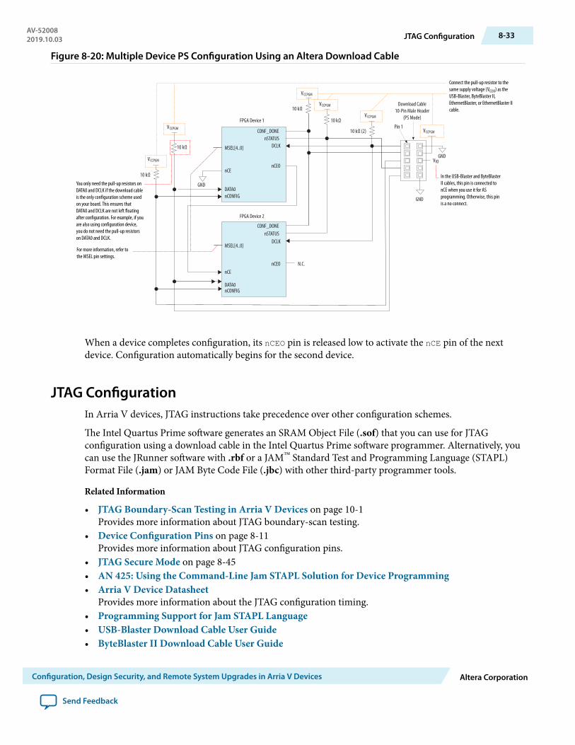
Figure 8-20: Multiple Device PS Configuration Using an Altera Download Cable
FPGA Device 1
FPGA Device 2
nCE
nCONFIG
CONF_DONE
DCLK
nCE
nCONFIG
CONF_DONE
DCLK
nCEO
GND
VCCPGM
VCCPGM
VCCPGM
VCCPGM
VCCPGM
nSTATUS
nSTATUS
DATA0
DATA0
GND
10 kΩ
10 kΩ
Pin 1
nCEO N.C.
GNDVIO
MSEL[4..0]
MSEL[4..0]
VCCPGM
10 kΩ
10 kΩ
10 kΩ (2)
You only need the pull-up resistors on DATA0 and DCLK if the download cable is the only configuration scheme used on your board. This ensures that DATA0 and DCLK are not left floating after configuration. For example, if you are also using configuration device, you do not need the pull-up resistors on DATA0 and DCLK.
For more information, refer to the MSEL pin settings.
Download Cable10-Pin Male Header
(PS Mode)
In the USB-Blaster and ByteBlaster II cables, this pin is connected to nCE when you use it for AS programming. Otherwise, this pin is a no connect.
Connect the pull-up resistor to the same supply voltage (VCCIO) as the USB-Blaster, ByteBlaster II, EthernetBlaster, or EthernetBlaster II cable.
When a device completes configuration, its nCEO pin is released low to activate the nCE pin of the nextdevice. Configuration automatically begins for the second device.
JTAG ConfigurationIn Arria V devices, JTAG instructions take precedence over other configuration schemes.
The Intel Quartus Prime software generates an SRAM Object File (.sof) that you can use for JTAGconfiguration using a download cable in the Intel Quartus Prime software programmer. Alternatively, youcan use the JRunner software with .rbf or a JAM™ Standard Test and Programming Language (STAPL)Format File (.jam) or JAM Byte Code File (.jbc) with other third-party programmer tools.
Related Information
• JTAG Boundary-Scan Testing in Arria V Devices on page 10-1Provides more information about JTAG boundary-scan testing.
• Device Configuration Pins on page 8-11Provides more information about JTAG configuration pins.
• JTAG Secure Mode on page 8-45• AN 425: Using the Command-Line Jam STAPL Solution for Device Programming• Arria V Device Datasheet
Provides more information about the JTAG configuration timing.• Programming Support for Jam STAPL Language• USB-Blaster Download Cable User Guide• ByteBlaster II Download Cable User Guide
AV-520082019.10.03 JTAG Configuration 8-33
Configuration, Design Security, and Remote System Upgrades in Arria V Devices Altera Corporation
Send Feedback

• EthernetBlaster Communications Cable User Guide• EthernetBlaster II Communications Cable User Guide
JTAG Single-Device ConfigurationTo configure a single device in a JTAG chain, the programming software sets the other devices to thebypass mode. A device in a bypass mode transfers the programming data from the TDI pin to the TDO pinthrough a single bypass register. The configuration data is available on the TDO pin one clock cycle later.
The Intel Quartus Prime software can use the CONF_DONE pin to verify the completion of the configurationprocess through the JTAG port:
• CONF_DONE pin is low—indicates that configuration has failed.• CONF_DONE pin is high—indicates that configuration was successful.
After the configuration data is transmitted serially using the JTAG TDI port, the TCK port is clocked anadditional 1,222 cycles to perform device initialization.
To configure an Arria V device using a download cable, connect the device as shown in the followingfigure.
Figure 8-21: JTAG Configuration of a Single Device Using a Download Cable
FPGA Device
DCLK
nCONFIGCONF_DONE
GNDGND
nSTATUSTDI
TMS
TDOTCK
Pin 1
nCE
GND
GND
nCEON.C.
MSEL[4..0]
VCCPGM VCCPGM
10 kΩ 10 kΩ
VCCPD
1 kΩ
VCCPD
VCCPD
The resistor value can vary from 1 kΩ to 10 kΩ. Perform signal integrity analysis to select the resistor value for your setup.
Connect the pull-up resistor VCCPD.
Download Cable10-Pin Male Header
(JTAG Mode) (Top View)
If you only use the JTAG configuration, connect nCONFIG to VCCPGM and MSEL[4..0] to GND. Pull DCLK either high or low whichever is convenient on your board. If you are using JTAG in conjunction with another configuration scheme, connect MSEL[4..0], nCONFIG, and DCLK based on the selected configuration scheme.
To configure Arria V device using a microprocessor, connect the device as shown in the following figure.You can use JRunner as your software driver.
8-34 JTAG Single-Device ConfigurationAV-52008
2019.10.03
Altera Corporation Configuration, Design Security, and Remote System Upgrades in Arria V Devices
Send Feedback

Figure 8-22: JTAG Configuration of a Single Device Using a Microprocessor
Microprocessor
CONF_DONEnSTATUS
nCE
nCONFIG
FPGA Device
Memory
ADDR
GND
DCLKTDITCKTMS
nCEO N.C.MSEL[4..0]
DATA
TDO
10 kΩ10 kΩ
VCCPGM VCCPGM
Connect the pull-up resistor to a supply that provides an acceptable input signal for all FPGA devices in the chain. VCCPGM must be high enough to meet the VIH specification of the I/O on the device.
The microprocessor must use the same I/O standard as VCCPD to drive the JTAG pins.
If you only use the JTAG configuration, connect nCONFIG to VCCPGM and MSEL[4..0] to GND. Pull DCLK high or low. If you are using JTAG in conjunction with another configuration scheme, set the MSEL[4..0] pins and tie nCONFIG and DCLK based on the selected configuration scheme.
Related InformationAN 414: The JRunner Software Driver: An Embedded Solution for PLD JTAG Configuration
JTAG Multi-Device ConfigurationYou can configure multiple devices in a JTAG chain.
Pin Connections and Guidelines
Observe the following pin connections and guidelines for this configuration setup:
• Isolate the CONF_DONE and nSTATUS pins to allow each device to enter user mode independently.• One JTAG-compatible header is connected to several devices in a JTAG chain. The number of devices
in the chain is limited only by the drive capability of the download cable.• If you have four or more devices in a JTAG chain, buffer the TCK, TDI, and TMS pins with an on-board
buffer. You can also connect other Altera devices with JTAG support to the chain.• JTAG-chain device programming is ideal when the system contains multiple devices or when testing
your system using the JTAG boundary-scan testing (BST) circuitry.
Using a Download Cable
The following figure shows a multi-device JTAG configuration.
AV-520082019.10.03 JTAG Multi-Device Configuration 8-35
Configuration, Design Security, and Remote System Upgrades in Arria V Devices Altera Corporation
Send Feedback
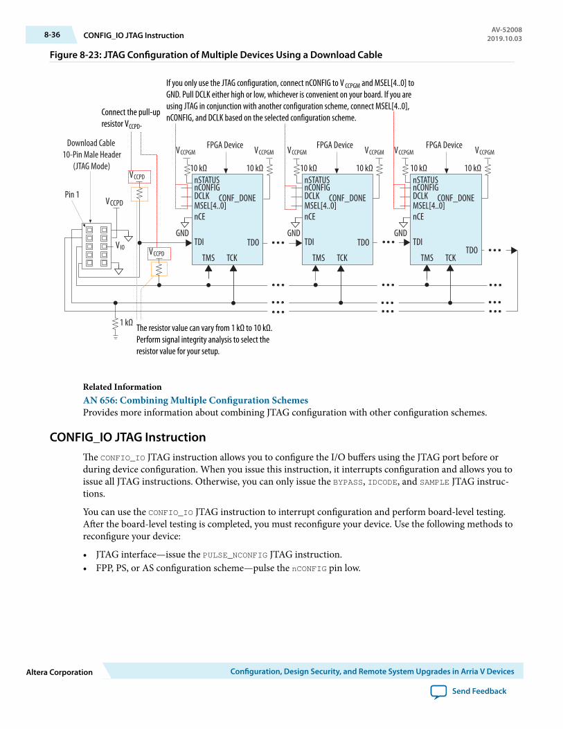
Figure 8-23: JTAG Configuration of Multiple Devices Using a Download Cable
TMS TCK
TDI TDO
VCCPD
VCCPD
VCCPD
Pin 1
nSTATUSnCONFIG
MSEL[4..0]nCE
GND GND GND
VCCPGM VCCPGM VCCPGM VCCPGM VCCPGM VCCPGM
CONF_DONE
V IO
FPGA Device FPGA Device FPGA Device
1 kΩ
10 kΩ 10 kΩ 10 kΩ 10 kΩ 10 kΩ 10 kΩ
DCLK
TMS TCK
TDI TDO
nSTATUSnCONFIG
MSEL[4..0]nCE
CONF_DONEDCLK
TMS TCK
TDITDO
nSTATUSnCONFIG
MSEL[4..0]nCE
CONF_DONEDCLK
If you only use the JTAG configuration, connect nCONFIG to V CCPGM and MSEL[4..0] to GND. Pull DCLK either high or low, whichever is convenient on your board. If you are using JTAG in conjunction with another configuration scheme, connect MSEL[4..0], nCONFIG, and DCLK based on the selected configuration scheme.
The resistor value can vary from 1 kΩ to 10 kΩ. Perform signal integrity analysis to select the resistor value for your setup.
Download Cable 10-Pin Male Header
(JTAG Mode)
Connect the pull-up resistor VCCPD.
Related InformationAN 656: Combining Multiple Configuration SchemesProvides more information about combining JTAG configuration with other configuration schemes.
CONFIG_IO JTAG InstructionThe CONFIO_IO JTAG instruction allows you to configure the I/O buffers using the JTAG port before orduring device configuration. When you issue this instruction, it interrupts configuration and allows you toissue all JTAG instructions. Otherwise, you can only issue the BYPASS, IDCODE, and SAMPLE JTAG instruc‐tions.
You can use the CONFIO_IO JTAG instruction to interrupt configuration and perform board-level testing.After the board-level testing is completed, you must reconfigure your device. Use the following methods toreconfigure your device:
• JTAG interface—issue the PULSE_NCONFIG JTAG instruction.• FPP, PS, or AS configuration scheme—pulse the nCONFIG pin low.
8-36 CONFIG_IO JTAG InstructionAV-52008
2019.10.03
Altera Corporation Configuration, Design Security, and Remote System Upgrades in Arria V Devices
Send Feedback

Configuration Data CompressionArria V devices can receive compressed configuration bitstream and decompress the data in real-timeduring configuration. Preliminary data indicates that compression typically reduces the configuration filesize by 30% to 55% depending on the design.
Decompression is supported in all configuration schemes except the JTAG configuration scheme.
You can enable compression before or after design compilation.
Enabling Compression Before Design CompilationTo enable compression before design compilation, follow these steps:
1. On the Assignment Menu, click Device.2. Select your Arria V device and then click Device and Pin Options.3. In the Device and Pin Options window, select Configuration under the Category list and turn on
Generate compressed bitstreams.
Enabling Compression After Design CompilationTo enable compression after design compilation, follow these steps:
1. On the File menu, click Convert Programming Files.2. Select the programming file type (.pof, .sof, .hex, .hexout, .rbf, or .ttf). For POF output files, select a
configuration device.3. Under the Input files to convert list, select SOF Data.4. Click Add File and select an Arria V device .sof.5. Select the name of the file you added to the SOF Data area and click Properties.6. Turn on the Compression check box.
Using Compression in Multi-Device ConfigurationThe following figure shows a chain of two Arria V devices. Compression is only enabled for the firstdevice.
This setup is supported by the AS or PS multi-device configuration only.
AV-520082019.10.03 Configuration Data Compression 8-37
Configuration, Design Security, and Remote System Upgrades in Arria V Devices Altera Corporation
Send Feedback

Figure 8-24: Compressed and Uncompressed Serial Configuration Data in the Same Configuration File
nCE
GND
nCEO
FPGADevice 1
FPGA Device 2
nCE nCEO N.C.
Serial Configuration Data
EPCS, EPCQ, orExternal Host
DecompressionController
CompressedConfiguration
Data
UncompressedConfiguration
Data
For the FPP configuration scheme, a combination of compressed and uncompressed configuration in thesame multi-device configuration chain is not allowed because of the difference on the DCLK-to-DATA[]ratio.
Remote System UpgradesArria V devices contain dedicated remote system upgrade circuitry. You can use this feature to upgradeyour system from a remote location.
Figure 8-25: Arria V Remote System Upgrade Block Diagram
DevelopmentLocation
FPGA Configuration
FPGARemote System
Upgrade Circuitry
Data
DataData
ConfigurationMemory
2
3
4
1
You can design your system to manage remote upgrades of the application configuration images in theconfiguration device. The following list is the sequence of the remote system upgrade:
1. The logic (embedded processor or user logic) in the Arria V device receives a configuration image froma remote location. You can connect the device to the remote source using communication protocolssuch as TCP/IP, PCI, user datagram protocol (UDP), UART, or a proprietary interface.
2. The logic stores the configuration image in non-volatile configuration memory.3. The logic starts reconfiguration cycle using the newly received configuration image.4. When an error occurs, the circuitry detects the error, reverts to a safe configuration image, and
provides error status to your design.
8-38 Remote System UpgradesAV-52008
2019.10.03
Altera Corporation Configuration, Design Security, and Remote System Upgrades in Arria V Devices
Send Feedback

Configuration ImagesEach Arria V device in your system requires one factory image. The factory image is a user-definedconfiguration image that contains logic to perform the following:
• Processes errors based on the status provided by the dedicated remote system upgrade circuitry.• Communicates with the remote host, receives new application images, and stores the images in the
local non-volatile memory device.• Determines the application image to load into the Arria V device.• Enables or disables the user watchdog timer and loads its time-out value.• Instructs the dedicated remote system upgrade circuitry to start a reconfiguration cycle.
You can also create one or more application images for the device. An application image contains selectedfunctionalities to be implemented in the target device.
Store the images at the following locations in the EPCS or EPCQ devices:
• Factory configuration image—PGM[23..0] = 24'h000000 start address on the EPCS or EPCQ device.• Application configuration image—any sector boundary. Altera recommends that you store only one
image at one sector boundary.
When you are using EPCQ 256, ensure that the application configuration image address granularity is32'h00000100. The granularity requirement is having the most significant 24 bits of the 32 bits startaddress written to PGM[23..0] bits.
Note: If you are not using the Intel Quartus Prime software or SRunner software for EPCQ 256 program‐ming, put your EPCQ 256 device into four-byte addressing mode before you program andconfigure your device.
AV-520082019.10.03 Configuration Images 8-39
Configuration, Design Security, and Remote System Upgrades in Arria V Devices Altera Corporation
Send Feedback

Configuration Sequence in the Remote Update ModeFigure 8-26: Transitions Between Factory and Application Configurations in Remote Update Mode
Set Control Register and Reconfigure
Set Control Register and Reconfigure
Reload a Different Application
Application nConfiguration
Application 1 Configuration
Factory Configuration
(page 0)
Configuration Error
Configuration Error
Power Up
ConfigurationError
Reload a Different Application
Related InformationRemote System Upgrade State Machine on page 8-43A detailed description of the configuration sequence in the remote update mode.
Remote System Upgrade CircuitryThe remote system upgrade circuitry contains the remote system upgrade registers, watchdog timer, and astate machine that controls these components.
Note: If you are using the Altera Remote Update IP core, the IP core controls the RU_DOUT, RU_SHIFTnLD,RU_CAPTnUPDT, RU_CLK, RU_DIN, RU_nCONFIG, and RU_nRSTIMER signals internally to perform allthe related remote system upgrade operations.
8-40 Configuration Sequence in the Remote Update ModeAV-52008
2019.10.03
Altera Corporation Configuration, Design Security, and Remote System Upgrades in Arria V Devices
Send Feedback

Figure 8-27: Remote System Upgrade Circuitry
Logic Array
Shift Register
Status Register (SR)[4..0]
Control Register [37..0]
din
capture
dout Bit [4..0]
Logic Array
clkout
RU_SHIFTnLD RU_CAPTnUPDT RU_CLK RU_DIN RU_nCONFIG RU_nRSTIMER
UserWatchdog
Timer
RU_DOUT
capture
clkin
update
Logic Array
capture
dinBit [37..0]dout
updateUpdate Register
[37..0]
Timeout
Remote System
Upgrade State
Machine
Internal Oscillator
Related InformationArria V Device DatasheetProvides more information about remote system upgrade circuitry timing specifications.
Enabling Remote System Upgrade CircuitryTo enable the remote system upgrade feature, follow these steps:
1. Select Active Serial x1/x4 or Configuration Device from the Configuration scheme list in theConfiguration page of the Device and Pin Options dialog box in the Intel Quartus Prime software.
2. Select Remote from the Configuration mode list in the Configuration page of the Device and PinOptions dialog box in the Intel Quartus Prime software.
Enabling this feature automatically turns on the Auto-restart configuration after error option.
Remote Update Intel FPGA IP core provides a memory-like interface to the remote system upgradecircuitry and handles the shift register read and write protocol in the Arria V device logic.
Related InformationAltera Remote Update IP Core User Guide
AV-520082019.10.03 Enabling Remote System Upgrade Circuitry 8-41
Configuration, Design Security, and Remote System Upgrades in Arria V Devices Altera Corporation
Send Feedback

Remote System Upgrade Registers
Table 8-10: Remote System Upgrade Registers
Register Description
Shift Accessible by the logic array and clocked by RU_CLK.
• Bits[4..0]—Contents of the status register are shifted into these bits.• Bits[37..0]—Contents of the update and control registers are shifted
into these bits.
Control This register is clocked by the 10-MHz internal oscillator. The contents of thisregister are shifted to the shift register for the user logic in the applicationconfiguration to read. When reconfiguration is triggered, this register isupdated with the contents of the update register.
Update This register is clocked by RU_CLK. The factory configuration updates thisregister by shifting data into the shift register and issuing an update. Whenreconfiguration is triggered, the contents of the update register are written tothe control register.
Status After each reconfiguration, the remote system upgrade circuitry updates thisregister to indicate the event that triggered the reconfiguration. This register isclocked by the 10-MHz internal oscillator.
Related Information
• Control Register on page 8-42• Status Register on page 8-43
Control Register
Table 8-11: Control Register Bits
Bit Name ResetValue(34)
Description
0 AnF 1'b0 Application not Factory bit. Indicates theconfiguration image type currently loaded inthe device; 0 for factory image and 1 forapplication image. When this bit is 1, theaccess to the control register is limited to readonly and the watchdog timer is enabled.
Factory configuration design must set this bitto 1 before triggering reconfiguration usingan application configuration image.
(34) This is the default value after the device exits POR and during reconfiguration back to the factory configura‐tion image.
8-42 Remote System Upgrade RegistersAV-52008
2019.10.03
Altera Corporation Configuration, Design Security, and Remote System Upgrades in Arria V Devices
Send Feedback
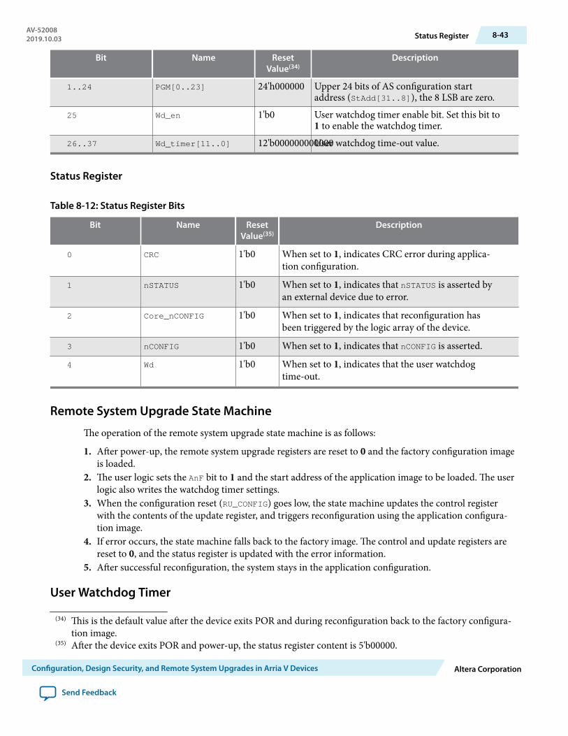
Bit Name ResetValue(34)
Description
1..24 PGM[0..23] 24'h000000 Upper 24 bits of AS configuration startaddress (StAdd[31..8]), the 8 LSB are zero.
25 Wd_en 1'b0 User watchdog timer enable bit. Set this bit to1 to enable the watchdog timer.
26..37 Wd_timer[11..0] 12'b000000000000User watchdog time-out value.
Status Register
Table 8-12: Status Register Bits
Bit Name ResetValue(35)
Description
0 CRC 1'b0 When set to 1, indicates CRC error during applica‐tion configuration.
1 nSTATUS 1'b0 When set to 1, indicates that nSTATUS is asserted byan external device due to error.
2 Core_nCONFIG 1'b0 When set to 1, indicates that reconfiguration hasbeen triggered by the logic array of the device.
3 nCONFIG 1'b0 When set to 1, indicates that nCONFIG is asserted.
4 Wd 1'b0 When set to 1, indicates that the user watchdogtime-out.
Remote System Upgrade State Machine
The operation of the remote system upgrade state machine is as follows:
1. After power-up, the remote system upgrade registers are reset to 0 and the factory configuration imageis loaded.
2. The user logic sets the AnF bit to 1 and the start address of the application image to be loaded. The userlogic also writes the watchdog timer settings.
3. When the configuration reset (RU_CONFIG) goes low, the state machine updates the control registerwith the contents of the update register, and triggers reconfiguration using the application configura‐tion image.
4. If error occurs, the state machine falls back to the factory image. The control and update registers arereset to 0, and the status register is updated with the error information.
5. After successful reconfiguration, the system stays in the application configuration.
User Watchdog Timer
(34) This is the default value after the device exits POR and during reconfiguration back to the factory configura‐tion image.
(35) After the device exits POR and power-up, the status register content is 5'b00000.
AV-520082019.10.03 Status Register 8-43
Configuration, Design Security, and Remote System Upgrades in Arria V Devices Altera Corporation
Send Feedback

The user watchdog timer prevents a faulty application configuration from stalling the device indefinitely.You can use the timer to detect functional errors when an application configuration is successfully loadedinto the device. The timer is automatically disabled in the factory configuration; enabled in the applicationconfiguration.
Note: If you do not want this feature in the application configuration, you need to turn off this feature bysetting the Wd_en bit to 1'b0 in the update register during factory configuration user modeoperation. You cannot disable this feature in the application configuration.
The counter is 29 bits wide and has a maximum count value of 229. When specifying the user watchdogtimer value, specify only the most significant 12 bits. The granularity of the timer setting is 217 cycles. Thecycle time is based on the frequency of the user watchdog timer internal oscillator.
The timer begins counting as soon as the application configuration enters user mode. When the timerexpires, the remote system upgrade circuitry generates a time-out signal, updates the status register, andtriggers the loading of the factory configuration image. To reset the time, assert RU_nRSTIMER.
Related InformationArria V Device DatasheetProvides more information about the operating range of the user watchdog internal oscillator's frequency.
Design Security
The Arria V design security feature supports the following capabilities:
• Enhanced built-in advanced encryption standard (AES) decryption block to support 256-bit keyindustry-standard design security algorithm (FIPS-197 Certified)
• Volatile and non-volatile key programming support• Secure operation mode for both volatile and non-volatile key through tamper protection bit setting• Limited accessible JTAG instruction during power-up in the JTAG secure mode• Supports board-level testing• Supports in-socket key programming for non-volatile key• Available in all configuration schemes except JTAG• Supports both remote system upgrades and compression features
The Arria V design security feature provides the following security protection for your designs:
• Security against copying—the security key is securely stored in the Arria V device and cannot be readout through any interface. In addition, as configuration file read-back is not supported in Arria Vdevices, your design information cannot be copied.
• Security against reverse engineering—reverse engineering from an encrypted configuration file is verydifficult and time consuming because the Arria V configuration file formats are proprietary and the filecontains millions of bits that require specific decryption.
• Security against tampering—After you set the tamper protection bit, the Arria V device can only acceptconfiguration files encrypted with the same key. Additionally, programming through the JTAGinterface and configuration interface is blocked.
When you use compression with the design security feature, the configuration file is first compressed andthen encrypted using the Intel Quartus Prime software. During configuration, the device first decrypts andthen decompresses the configuration file.
8-44 Design SecurityAV-52008
2019.10.03
Altera Corporation Configuration, Design Security, and Remote System Upgrades in Arria V Devices
Send Feedback
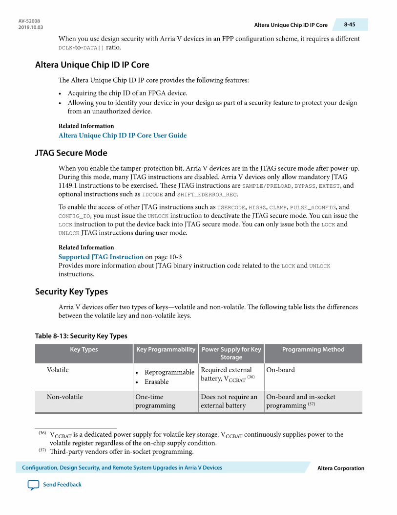
When you use design security with Arria V devices in an FPP configuration scheme, it requires a differentDCLK-to-DATA[] ratio.
Altera Unique Chip ID IP Core
The Altera Unique Chip ID IP core provides the following features:
• Acquiring the chip ID of an FPGA device.• Allowing you to identify your device in your design as part of a security feature to protect your design
from an unauthorized device.
Related InformationAltera Unique Chip ID IP Core User Guide
JTAG Secure Mode
When you enable the tamper-protection bit, Arria V devices are in the JTAG secure mode after power-up.During this mode, many JTAG instructions are disabled. Arria V devices only allow mandatory JTAG1149.1 instructions to be exercised. These JTAG instructions are SAMPLE/PRELOAD, BYPASS, EXTEST, andoptional instructions such as IDCODE and SHIFT_EDERROR_REG.
To enable the access of other JTAG instructions such as USERCODE, HIGHZ, CLAMP, PULSE_nCONFIG, andCONFIG_IO, you must issue the UNLOCK instruction to deactivate the JTAG secure mode. You can issue theLOCK instruction to put the device back into JTAG secure mode. You can only issue both the LOCK andUNLOCK JTAG instructions during user mode.
Related InformationSupported JTAG Instruction on page 10-3Provides more information about JTAG binary instruction code related to the LOCK and UNLOCKinstructions.
Security Key Types
Arria V devices offer two types of keys—volatile and non-volatile. The following table lists the differencesbetween the volatile key and non-volatile keys.
Table 8-13: Security Key Types
Key Types Key Programmability Power Supply for KeyStorage
Programming Method
Volatile • Reprogrammable• Erasable
Required externalbattery, VCCBAT (36)
On-board
Non-volatile One-timeprogramming
Does not require anexternal battery
On-board and in-socketprogramming (37)
(36) VCCBAT is a dedicated power supply for volatile key storage. VCCBAT continuously supplies power to thevolatile register regardless of the on-chip supply condition.
(37) Third-party vendors offer in-socket programming.
AV-520082019.10.03 Altera Unique Chip ID IP Core 8-45
Configuration, Design Security, and Remote System Upgrades in Arria V Devices Altera Corporation
Send Feedback
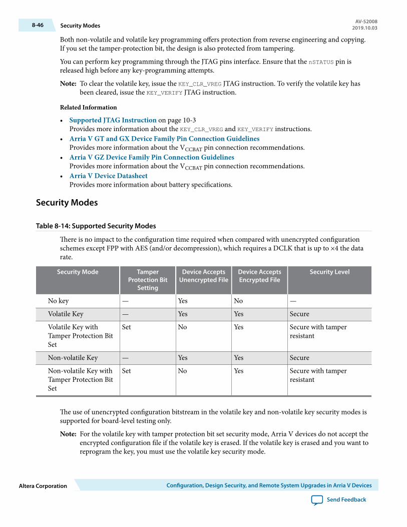
Both non-volatile and volatile key programming offers protection from reverse engineering and copying.If you set the tamper-protection bit, the design is also protected from tampering.
You can perform key programming through the JTAG pins interface. Ensure that the nSTATUS pin isreleased high before any key-programming attempts.
Note: To clear the volatile key, issue the KEY_CLR_VREG JTAG instruction. To verify the volatile key hasbeen cleared, issue the KEY_VERIFY JTAG instruction.
Related Information
• Supported JTAG Instruction on page 10-3Provides more information about the KEY_CLR_VREG and KEY_VERIFY instructions.
• Arria V GT and GX Device Family Pin Connection GuidelinesProvides more information about the VCCBAT pin connection recommendations.
• Arria V GZ Device Family Pin Connection GuidelinesProvides more information about the VCCBAT pin connection recommendations.
• Arria V Device DatasheetProvides more information about battery specifications.
Security Modes
Table 8-14: Supported Security Modes
There is no impact to the configuration time required when compared with unencrypted configurationschemes except FPP with AES (and/or decompression), which requires a DCLK that is up to ×4 the datarate.
Security Mode TamperProtection Bit
Setting
Device AcceptsUnencrypted File
Device AcceptsEncrypted File
Security Level
No key — Yes No —
Volatile Key — Yes Yes Secure
Volatile Key withTamper Protection BitSet
Set No Yes Secure with tamperresistant
Non-volatile Key — Yes Yes Secure
Non-volatile Key withTamper Protection BitSet
Set No Yes Secure with tamperresistant
The use of unencrypted configuration bitstream in the volatile key and non-volatile key security modes issupported for board-level testing only.
Note: For the volatile key with tamper protection bit set security mode, Arria V devices do not accept theencrypted configuration file if the volatile key is erased. If the volatile key is erased and you want toreprogram the key, you must use the volatile key security mode.
8-46 Security ModesAV-52008
2019.10.03
Altera Corporation Configuration, Design Security, and Remote System Upgrades in Arria V Devices
Send Feedback

Enabling the tamper protection bit disables the test mode in Arria V devices and disables programmingthrough the JTAG interface. This process is irreversible and prevents Altera from carrying out failureanalysis.
Design Security Implementation StepsFigure 8-28: Design Security Implementation Steps
AES KeyProgramming File Key Storage
Encrypted Configuration
File
AES Encryptor
Quartus Prime Software
Memory orConfiguration
Device
FPGA Device
AES Decryption
Step 3
Step 1
Step 1
Step 2
256-bit User-DefinedKey
Step 4
To carry out secure configuration, follow these steps:
1. The Intel Quartus Prime software generates the design security key programming file and encrypts theconfiguration data using the user-defined 256-bit security key.
2. Store the encrypted configuration file in the external memory.3. Program the AES key programming file into the Arria V device through a JTAG interface.4. Configure the Arria V device. At the system power-up, the external memory device sends the
encrypted configuration file to the Arria V device.
Configuration, Design Security, and Remote System Upgrades in Arria VDevices Revision History
DocumentVersion
Changes
2019.10.03 Added a note to Device Configuration Pins to state that the DCLK, AS_DATA0/ASDO, AS_DATA1,AS_DATA2, AS_DATA3, and nCSO pins have 25 kOhm pull-up resistors when the MSEL pins areset to AS configuration scheme.
2018.08.09 • Updated the Active Serial Configuration topic.• Updated Figure: AS Configuration Timing Waveform.
AV-520082019.10.03 Design Security Implementation Steps 8-47
Configuration, Design Security, and Remote System Upgrades in Arria V Devices Altera Corporation
Send Feedback

Date Version Changes
December2017
2017.12.15 Added description in the I/O Standards and Drive Strength for Configura‐tion Pins table.
December2016
2016.12.09 Changed the term "configuration mode" to "configuration scheme" whenreferring to a configuration scheme.
August 2016 2016.08.24 Added note to Power Up and Reset states in the Configuration Sequencefor Cyclone V Devices diagram.
June 2016 2016.06.10 • Added a note to specify the time between nCSO falling edge to firsttoggle of DCLK is more than 15ns in AS Configuration Timing figure.
December2015
2015.12.21 • Changed instances of Quartus II to Quartus Prime.• Added the CvP_CONFDONE pin to the Configuration Pin Summary for
Arria V Devices table.• Added the I/O Standards and Drive Strength for Configuration Pins
table.
June 2015 2015.06.12 • Added timing waveforms for FPP, AS, and PS configuration.• Updated the Trace Length and Loading Guideline section.
January 2015 2015.01.23 • Added the Transmitting Configuration Data section.• Updated the Configuration Images section.
June 2014 2014.06.30 • Updated Figure 8-17: JTAG Configuration of a Single Device Using aDownload Cable.
• Updated Figure 8-19: JTAG Configuration of Multiple Devices Usinga Download Cable.
• Updated the maximum clock rate for Partial Reconfiguration in Table8-1.
• Updated the MSEL pin settings recommendation in the MSEL PinSettings section.
January 2014 2014.01.10 • Added a link to the FPGA Manager chapter for details about theMSEL pin settings for the HPS in SoC FPGA devices.
• Updated the VCCPD Pin section.• Updated the Enabling Remote System Upgrade Circuitry section.• Updated the Configuration Pin Summary section.• Updated Figure 8-3, Figure 8-7, and Figure 8-14.
June 2013 2013.06.11 Updated the Configuration Error Handling section.
May 2013 2013.05.10 Removed support for active serial multi-device configuration using thesame configuration data.
8-48 Configuration, Design Security, and Remote System Upgrades in Arria V DevicesRevision History
AV-520082019.10.03
Altera Corporation Configuration, Design Security, and Remote System Upgrades in Arria V Devices
Send Feedback

Date Version Changes
May 2013 2013.05.06 • Added link to the known document issues in the Knowledge Base.• Added the ALTCHIP_ID megafunction section.• Updated "Connection Setup for Programming the EPCS Using the
JTAG Interface" and "Connection Setup for Programming the EPCQUsing the JTAG Interface" figures.
• Added the nIO_PULLUP pin in Table 8-3: Configuration Pin Summaryfor Arria V Devices.
• Added links for AS, PS, FPP, and JTAG configuration timing to devicedatasheet.
• Moved all links to the Related Information section of respective topicsfor easy reference.
November2012
2012.11.19 • Added configuration modes and features for Arria V devices.• Added FPP x32 for Arria V GZ devices.• Added DATA[31..16] for Arria V GZ devices.• Reorganized content and updated template.
June 2012 2.0 Restructured the chapter.
November2011
1.1 Minor text edits.
October 2011 1.0 Initial release.
AV-520082019.10.03 Configuration, Design Security, and Remote System Upgrades in Arria V Devices
Revision History8-49
Configuration, Design Security, and Remote System Upgrades in Arria V Devices Altera Corporation
Send Feedback

SEU Mitigation for Arria V Devices 92019.10.03
AV-52009 Subscribe Send Feedback
This chapter describes the error detection features in Arria V devices. You can use these features tomitigate single event upset (SEU) or soft errors.
Related InformationArria V Device Handbook: Known IssuesLists the planned updates to the Arria V Device Handbook chapters.
Error Detection FeaturesThe on-chip error detection CRC circuitry allows you to perform the following operations without anyimpact on the fitting or performance of the device:
• Auto-detection of CRC errors during configuration.• Optional CRC error detection and identification in user mode.• Testing of error detection functions by deliberately injecting errors through the JTAG interface.
Configuration Error DetectionWhen the Intel Quartus Prime software generates the configuration bitstream, the software also computesa 16-bit CRC value for each frame. A configuration bitstream can contain more than one CRC valuesdepending on the number of data frames in the bitstream. The length of the data frame varies for eachdevice.
When a data frame is loaded into the FPGA during configuration, the precomputed CRC value shifts intothe CRC circuitry. At the same time, the CRC engine in the FPGA computes the CRC value for the dataframe and compares it against the precomputed CRC value. If both CRC values do not match, the nSTATUSpin is set to low to indicate a configuration error.
You can test the capability of this feature by modifying the configuration bitstream or intentionallycorrupting the bitstream during configuration.
User Mode Error DetectionIn user mode, the contents of the configured CRAM bits may be affected by soft errors. These soft errors,which are caused by an ionizing particle, are not common in Altera devices. However, high-reliability
Intel Corporation. All rights reserved. Intel, the Intel logo, Altera, Arria, Cyclone, Enpirion, MAX, Nios, Quartus and Stratix words and logos are trademarks ofIntel Corporation or its subsidiaries in the U.S. and/or other countries. Intel warrants performance of its FPGA and semiconductor products to currentspecifications in accordance with Intel's standard warranty, but reserves the right to make changes to any products and services at any time without notice.Intel assumes no responsibility or liability arising out of the application or use of any information, product, or service described herein except as expresslyagreed to in writing by Intel. Intel customers are advised to obtain the latest version of device specifications before relying on any published informationand before placing orders for products or services.*Other names and brands may be claimed as the property of others.
ISO9001:2015Registered
www.altera.com101 Innovation Drive, San Jose, CA 95134
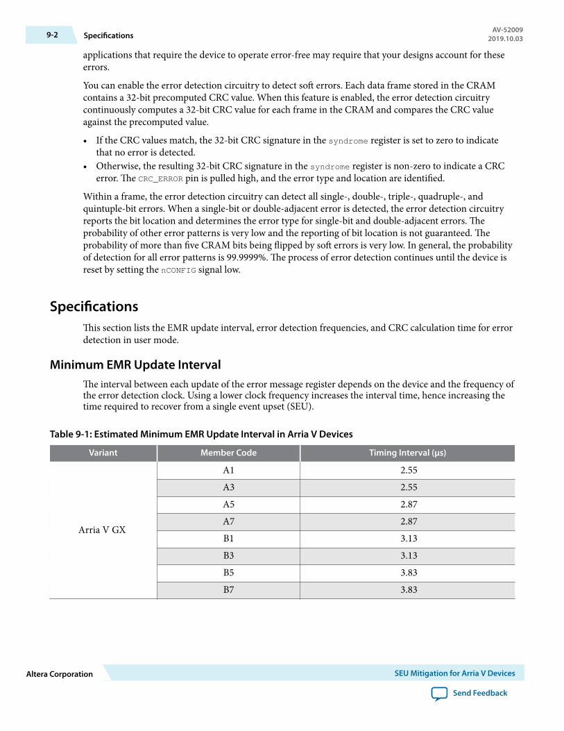
applications that require the device to operate error-free may require that your designs account for theseerrors.
You can enable the error detection circuitry to detect soft errors. Each data frame stored in the CRAMcontains a 32-bit precomputed CRC value. When this feature is enabled, the error detection circuitrycontinuously computes a 32-bit CRC value for each frame in the CRAM and compares the CRC valueagainst the precomputed value.
• If the CRC values match, the 32-bit CRC signature in the syndrome register is set to zero to indicatethat no error is detected.
• Otherwise, the resulting 32-bit CRC signature in the syndrome register is non-zero to indicate a CRCerror. The CRC_ERROR pin is pulled high, and the error type and location are identified.
Within a frame, the error detection circuitry can detect all single-, double-, triple-, quadruple-, andquintuple-bit errors. When a single-bit or double-adjacent error is detected, the error detection circuitryreports the bit location and determines the error type for single-bit and double-adjacent errors. Theprobability of other error patterns is very low and the reporting of bit location is not guaranteed. Theprobability of more than five CRAM bits being flipped by soft errors is very low. In general, the probabilityof detection for all error patterns is 99.9999%. The process of error detection continues until the device isreset by setting the nCONFIG signal low.
SpecificationsThis section lists the EMR update interval, error detection frequencies, and CRC calculation time for errordetection in user mode.
Minimum EMR Update IntervalThe interval between each update of the error message register depends on the device and the frequency ofthe error detection clock. Using a lower clock frequency increases the interval time, hence increasing thetime required to recover from a single event upset (SEU).
Table 9-1: Estimated Minimum EMR Update Interval in Arria V Devices
Variant Member Code Timing Interval (µs)
Arria V GX
A1 2.55A3 2.55A5 2.87A7 2.87B1 3.13B3 3.13B5 3.83B7 3.83
9-2 SpecificationsAV-52009
2019.10.03
Altera Corporation SEU Mitigation for Arria V Devices
Send Feedback

Variant Member Code Timing Interval (µs)
Arria V GT
C3 2.55C7 2.87D3 3.13D7 3.83
Arria V GZ
E1 2.43E3 2.43E5 2.99E7 2.99
Arria V SXB3 3.83B5 3.83
Arria V STD3 3.83D5 3.83
Error Detection FrequencyYou can control the speed of the error detection process by setting the division factor of the clockfrequency in the Intel Quartus Prime software. The divisor is 2n, where n can be any value listed in thefollowing table.
The speed of the error detection process for each data frame is determined by the following equation:
Figure 9-1: Error Detection Frequency Equation
Error Detection Frequency =Internal Oscillator Frequency
2 n
Table 9-2: Error Detection Frequency Range for Arria V Devices
The following table lists the frequencies and valid values of n.Internal Oscillator
Frequency
Error Detection Frequencyn Divisor Range
Maximum Minimum
100 MHz 100 MHz 390 kHz 0, 1, 2, 3, 4, 5, 6, 7, 8 1 – 256
CRC Calculation Time For Entire DeviceWhile the CRC calculation is done on a per frame basis, it is important to know the time taken tocomplete CRC calculations for the entire device. The entire device detection time is the time taken to doCRC calculations on every frame in the device. This time depends on the device and the error detectionclock frequency. The error detection clock frequency also depends on the device and on the internaloscillator frequency, which varies from 42.6 MHz to 100 MHz.
AV-520092019.10.03 Error Detection Frequency 9-3
SEU Mitigation for Arria V Devices Altera Corporation
Send Feedback
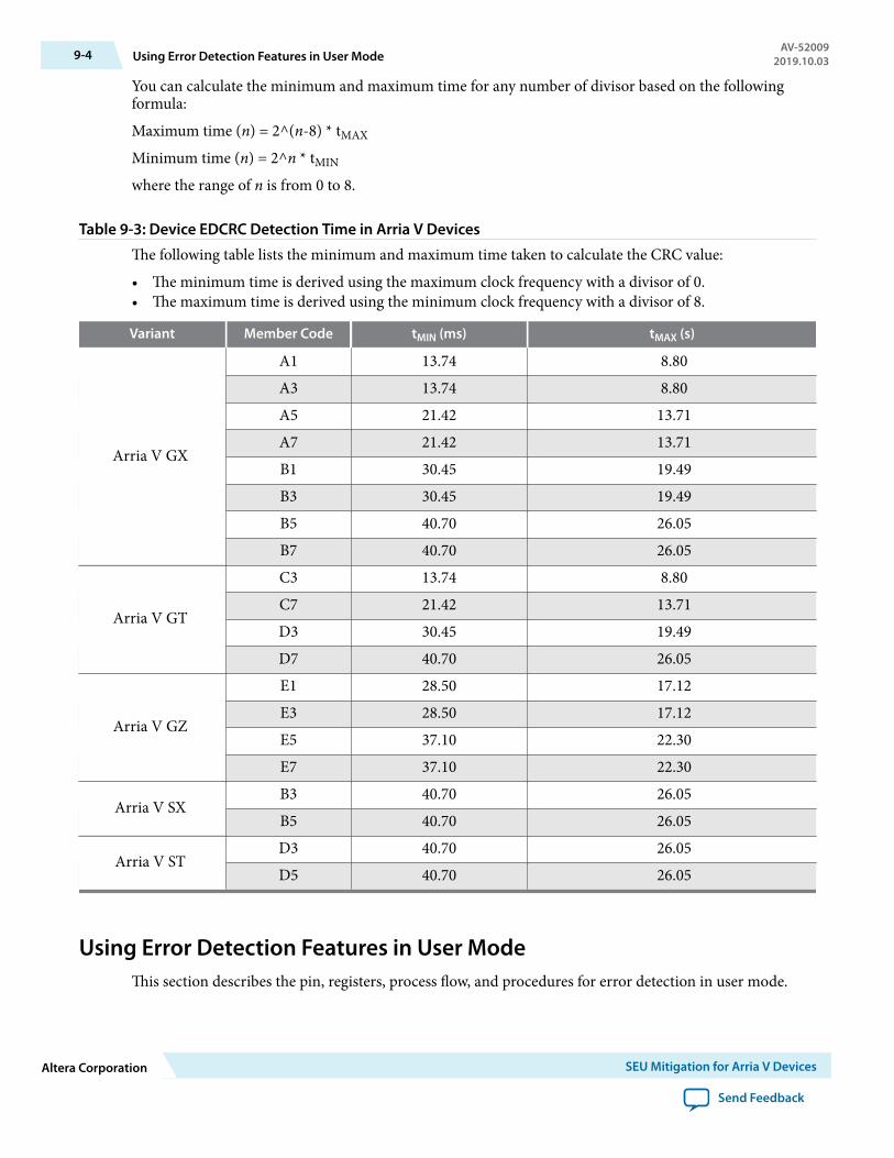
You can calculate the minimum and maximum time for any number of divisor based on the followingformula:
Maximum time (n) = 2^(n-8) * tMAX
Minimum time (n) = 2^n * tMIN
where the range of n is from 0 to 8.
Table 9-3: Device EDCRC Detection Time in Arria V Devices
The following table lists the minimum and maximum time taken to calculate the CRC value:
• The minimum time is derived using the maximum clock frequency with a divisor of 0.• The maximum time is derived using the minimum clock frequency with a divisor of 8.
Variant Member Code tMIN (ms) tMAX (s)
Arria V GX
A1 13.74 8.80A3 13.74 8.80A5 21.42 13.71A7 21.42 13.71B1 30.45 19.49B3 30.45 19.49B5 40.70 26.05B7 40.70 26.05
Arria V GT
C3 13.74 8.80C7 21.42 13.71D3 30.45 19.49D7 40.70 26.05
Arria V GZ
E1 28.50 17.12E3 28.50 17.12E5 37.10 22.30E7 37.10 22.30
Arria V SXB3 40.70 26.05B5 40.70 26.05
Arria V STD3 40.70 26.05D5 40.70 26.05
Using Error Detection Features in User ModeThis section describes the pin, registers, process flow, and procedures for error detection in user mode.
9-4 Using Error Detection Features in User ModeAV-52009
2019.10.03
Altera Corporation SEU Mitigation for Arria V Devices
Send Feedback
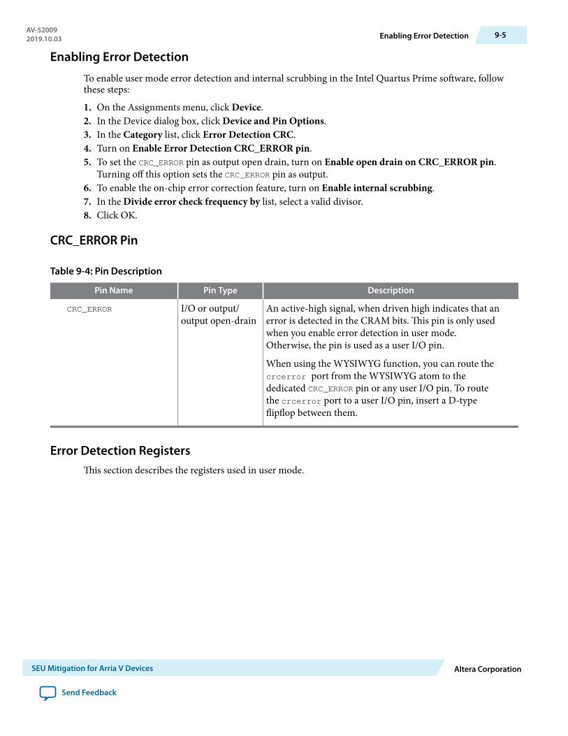
Enabling Error Detection
To enable user mode error detection and internal scrubbing in the Intel Quartus Prime software, followthese steps:
1. On the Assignments menu, click Device.2. In the Device dialog box, click Device and Pin Options.3. In the Category list, click Error Detection CRC.4. Turn on Enable Error Detection CRC_ERROR pin.5. To set the CRC_ERROR pin as output open drain, turn on Enable open drain on CRC_ERROR pin.
Turning off this option sets the CRC_ERROR pin as output.6. To enable the on-chip error correction feature, turn on Enable internal scrubbing.7. In the Divide error check frequency by list, select a valid divisor.8. Click OK.
CRC_ERROR Pin
Table 9-4: Pin Description
Pin Name Pin Type Description
CRC_ERROR I/O or output/output open-drain
An active-high signal, when driven high indicates that anerror is detected in the CRAM bits. This pin is only usedwhen you enable error detection in user mode.Otherwise, the pin is used as a user I/O pin.
When using the WYSIWYG function, you can route thecrcerror port from the WYSIWYG atom to thededicated CRC_ERROR pin or any user I/O pin. To routethe crcerror port to a user I/O pin, insert a D-typeflipflop between them.
Error Detection RegistersThis section describes the registers used in user mode.
AV-520092019.10.03 Enabling Error Detection 9-5
SEU Mitigation for Arria V Devices Altera Corporation
Send Feedback

Figure 9-2: Block Diagram for Error Detection in User ModeThe block diagram shows the registers and data flow in user mode.
Error Injection Block
JTAG TDO General Routing
CRC_ERROR
ReadbackBitstream withExpected CRC
ErrorDetection
State Machine
ControlSignals
32-bit Error DetectionCRC Calculation and Error Search Engine
SyndromeRegister
ErrorMessageRegister
JTAGUpdate
Register
UserUpdate
Register
JTAGShift
Register
UserShift
Register
FaultInjectionRegister
JTAGFault
InjectionRegister
Table 9-5: Error Detection Registers
Name Width(Bits)
Description
Syndrome register 32 Contains the 32-bit CRC signature calculated for thecurrent frame. If the CRC value is 0, the CRC_ERROR pin isdriven low to indicate no error. Otherwise, the pin ispulled high.
Error message register (EMR) 67 Contains error details for single-bit and double-adjacenterrors. The error detection circuitry updates this registereach time the circuitry detects an error. The Error MessageRegister Map figure shows the fields in this register and theError Type in EMR table lists the possible error types.
JTAG update register 67 This register is automatically updated with the contents ofthe EMR one clock cycle after the content of this register isvalidated. The JTAG update register includes a clockenable, which must be asserted before its contents arewritten to the JTAG shift register. This requirementensures that the JTAG update register is not overwrittenwhen its contents are being read by the JTAG shift register.
JTAG shift register 67 This register allows you to access the contents of the JTAGupdate register via the JTAG interface using the SHIFT_EDERROR_REG JTAG instruction.
9-6 Error Detection RegistersAV-52009
2019.10.03
Altera Corporation SEU Mitigation for Arria V Devices
Send Feedback

Name Width(Bits)
Description
User update register 67 This register is automatically updated with the contents ofthe EMR one clock cycle after the contents of this registerare validated. The user update register includes a clockenable, which must be asserted before its contents arewritten to the user shift register. This requirement ensuresthat the user update register is not overwritten when itscontents are being read by the user shift register.
User shift register 67 This register allows user logic to access the contents of theuser update register via the core interface.
JTAG fault injection register 46 You can use this register with the EDERROR_INJECT JTAGinstruction to inject errors in the bitstream. The JTAGFault Injection Register Map table lists the fields in thisregister.
Fault injection register 46 This register is updated with the contents of the JTAG faultinjection register.
Figure 9-3: Error Message Register Map
Syndrome Frame Address Byte Offset Bit Offset Error Type
MSB LSB
32 bits 16 bits 10 bits 2 bits 3 bits 4 bits
Double WordLocation
Table 9-6: Error Type in EMR
The following table lists the possible error types reported in the error type field in the EMR.Error Type
DescriptionBit 3 Bit 2 Bit 1 Bit 0
0 0 0 0 No CRC error.0 0 0 1 Location of a single-bit error is identified.0 0 1 0 Location of a double-adjacent error is identified.1 1 1 1 Error types other than single-bit and double-adjacent errors.
Table 9-7: JTAG Fault Injection Register Map
Field Name Bit Range Description
Error ByteValue
31:0 Contains the location of the bit error thatcorresponds to the error injection type to thisfield.
Byte Location 41:32 Contains the location of the injected error inthe first data frame.
AV-520092019.10.03 Error Detection Registers 9-7
SEU Mitigation for Arria V Devices Altera Corporation
Send Feedback

Field Name Bit Range Description
Error Type
45:42Specifies the following error types.
Bit 45 Bit 44 Bit 43 Bit 420 0 0 0 No error0 0 0 1 Single-bit error0 0 1 0 Double adjacent error
Error Detection ProcessWhen enabled, the user mode error detection process activates automatically when the FPGA enters usermode. The process continues to run until the device is reset even when an error is detected in the currentframe.
Figure 9-4: Error Detection Process Flow in User Mode
Yes
NoReceiveData Frame
Calculate andCompare
CRC Values
ErrorDetected?
Pull CRC_ERRORSignal Low for
32 Clock Cycles
Update Error Message Register
(Overwrite)
Search forError Location
DriveCRC_ERROR
Signal High
Timing
The CRC_ERROR pin is always driven low during CRC calculation. When an error occurs, the EDCRC hardblock takes 32 clock cycles to update the EMR, the pin is driven high once the EMR is updated. Therefore,you can start retrieving the contents of the EMR at the rising edge of the CRC_ERROR pin. The pin stayshigh until the current frame is read and then driven low again for 32 clock cycles. To ensure informationintegrity, complete the read operation within one frame of the CRC verification. The following diagramshows the timing of these events.
9-8 Error Detection ProcessAV-52009
2019.10.03
Altera Corporation SEU Mitigation for Arria V Devices
Send Feedback

Figure 9-5: Timing Requirements
No CRC Error CRC Error CRC Error
CRC Error No CRC Error No CRC Error
N N+1 N+2 N+3 N+4 N+5Frame
Data Integrity
Read Data Frame
CRC ERROR Pin
CRC Calculation(32 clock cycles)
Read Error MessageRegister (allowed time)
Read Error Messagefor frame N+1
Read Error Messagefor frame N+2
Read Error Messagefor frame N+4
Retrieving Error Information
You can retrieve the error information via the core interface or the JTAG interface using theSHIFT_EDERROR_REG JTAG instruction.
Recovering from CRC Errors
The system that hosts the FPGA must control device reconfiguration. To recover from a CRC error, drivethe nCONFIG signal low. The system waits for a safe time before reconfiguring the device. When reconfigu‐ration completes successfully, the FPGA operates as intended.
Related Information
• Error Detection Frequency on page 9-3Provides more information about the minimum and maximum error detection frequencies.
• Minimum EMR Update Interval on page 9-2Provides more information about the duration of each Arria Vdevice.
• Test Methodology of Error Detection and Recovery using CRC in Altera FPGA DevicesProvides more information about how to retrieve the error information.
Testing the Error Detection BlockYou can inject errors into the configuration data to test the error detection block. This error injectionmethodology provides design verification and system fault tolerance characterization.
Testing via the JTAG Interface
You can intentionally inject single or double-adjacent errors into the configuration data using theEDERROR_INJECT JTAG instruction.
AV-520092019.10.03 Testing the Error Detection Block 9-9
SEU Mitigation for Arria V Devices Altera Corporation
Send Feedback
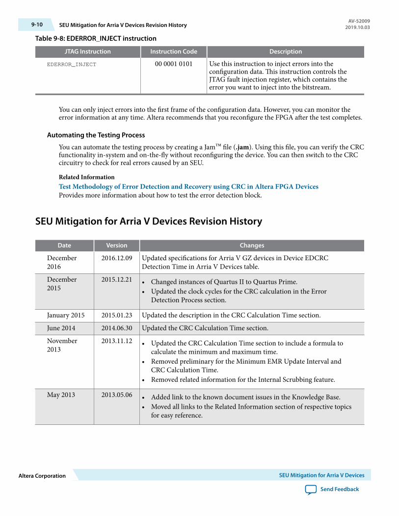
Table 9-8: EDERROR_INJECT instruction
JTAG Instruction Instruction Code Description
EDERROR_INJECT 00 0001 0101 Use this instruction to inject errors into theconfiguration data. This instruction controls theJTAG fault injection register, which contains theerror you want to inject into the bitstream.
You can only inject errors into the first frame of the configuration data. However, you can monitor theerror information at any time. Altera recommends that you reconfigure the FPGA after the test completes.
Automating the Testing Process
You can automate the testing process by creating a Jam™ file (.jam). Using this file, you can verify the CRCfunctionality in-system and on-the-fly without reconfiguring the device. You can then switch to the CRCcircuitry to check for real errors caused by an SEU.
Related InformationTest Methodology of Error Detection and Recovery using CRC in Altera FPGA DevicesProvides more information about how to test the error detection block.
SEU Mitigation for Arria V Devices Revision History
Date Version Changes
December2016
2016.12.09 Updated specifications for Arria V GZ devices in Device EDCRCDetection Time in Arria V Devices table.
December2015
2015.12.21 • Changed instances of Quartus II to Quartus Prime.• Updated the clock cycles for the CRC calculation in the Error
Detection Process section.
January 2015 2015.01.23 Updated the description in the CRC Calculation Time section.
June 2014 2014.06.30 Updated the CRC Calculation Time section.
November2013
2013.11.12 • Updated the CRC Calculation Time section to include a formula tocalculate the minimum and maximum time.
• Removed preliminary for the Minimum EMR Update Interval andCRC Calculation Time.
• Removed related information for the Internal Scrubbing feature.
May 2013 2013.05.06 • Added link to the known document issues in the Knowledge Base.• Moved all links to the Related Information section of respective topics
for easy reference.
9-10 SEU Mitigation for Arria V Devices Revision HistoryAV-52009
2019.10.03
Altera Corporation SEU Mitigation for Arria V Devices
Send Feedback
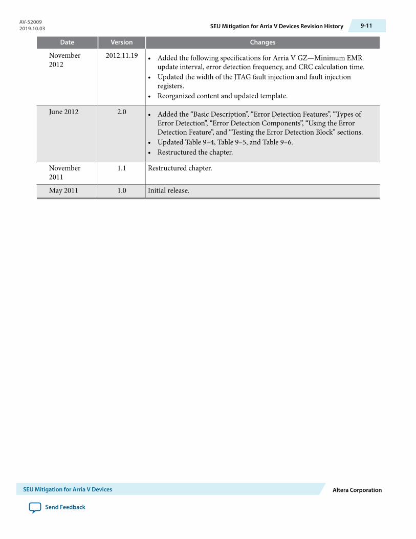
Date Version Changes
November2012
2012.11.19 • Added the following specifications for Arria V GZ—Minimum EMRupdate interval, error detection frequency, and CRC calculation time.
• Updated the width of the JTAG fault injection and fault injectionregisters.
• Reorganized content and updated template.
June 2012 2.0 • Added the “Basic Description”, “Error Detection Features”, “Types ofError Detection”, “Error Detection Components”, “Using the ErrorDetection Feature”, and “Testing the Error Detection Block” sections.
• Updated Table 9–4, Table 9–5, and Table 9–6.• Restructured the chapter.
November2011
1.1 Restructured chapter.
May 2011 1.0 Initial release.
AV-520092019.10.03 SEU Mitigation for Arria V Devices Revision History 9-11
SEU Mitigation for Arria V Devices Altera Corporation
Send Feedback
JTAG Boundary-Scan Testing in Arria V Devices 102019.10.03
AV-52010 Subscribe Send Feedback
This chapter describes the boundary-scan test (BST) features in Arria V devices.
Related Information
• JTAG Configuration on page 8-33Provides more information about JTAG configuration.
• Arria V Device Handbook: Known IssuesLists the planned updates to the Arria V Device Handbook chapters.
BST Operation ControlArria V GX, GT, SX, and ST devices support IEEE Std. 1149.1 BST. Arria V GZ devices supportIEEE Std. 1149.1 and IEEE Std. 1149.6 BST. You can perform BST on Arria V devices before, after, andduring configuration.
IDCODEThe IDCODE is unique for each Arria V device. Use this code to identify the devices in a JTAG chain.
Intel Corporation. All rights reserved. Intel, the Intel logo, Altera, Arria, Cyclone, Enpirion, MAX, Nios, Quartus and Stratix words and logos are trademarks ofIntel Corporation or its subsidiaries in the U.S. and/or other countries. Intel warrants performance of its FPGA and semiconductor products to currentspecifications in accordance with Intel's standard warranty, but reserves the right to make changes to any products and services at any time without notice.Intel assumes no responsibility or liability arising out of the application or use of any information, product, or service described herein except as expresslyagreed to in writing by Intel. Intel customers are advised to obtain the latest version of device specifications before relying on any published informationand before placing orders for products or services.*Other names and brands may be claimed as the property of others.
ISO9001:2015Registered
www.altera.com101 Innovation Drive, San Jose, CA 95134
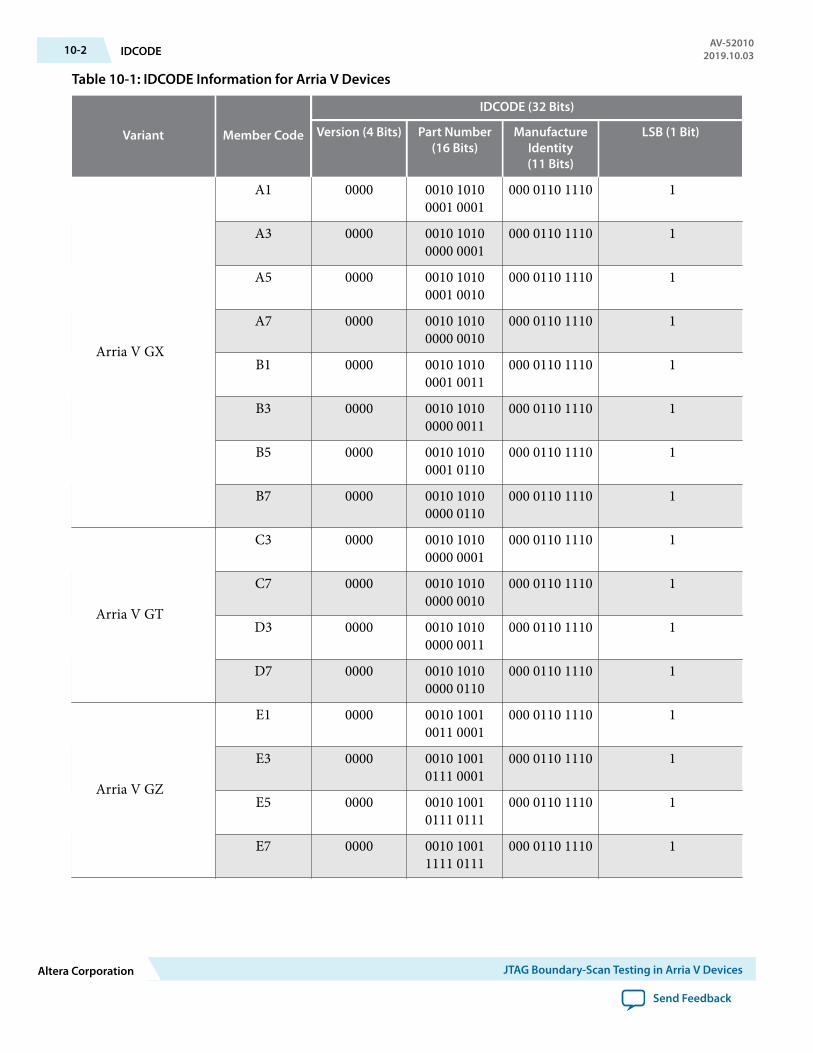
Table 10-1: IDCODE Information for Arria V Devices
Variant Member Code
IDCODE (32 Bits)
Version (4 Bits) Part Number(16 Bits)
ManufactureIdentity(11 Bits)
LSB (1 Bit)
Arria V GX
A1 0000 0010 10100001 0001
000 0110 1110 1
A3 0000 0010 10100000 0001
000 0110 1110 1
A5 0000 0010 10100001 0010
000 0110 1110 1
A7 0000 0010 10100000 0010
000 0110 1110 1
B1 0000 0010 10100001 0011
000 0110 1110 1
B3 0000 0010 10100000 0011
000 0110 1110 1
B5 0000 0010 10100001 0110
000 0110 1110 1
B7 0000 0010 10100000 0110
000 0110 1110 1
Arria V GT
C3 0000 0010 10100000 0001
000 0110 1110 1
C7 0000 0010 10100000 0010
000 0110 1110 1
D3 0000 0010 10100000 0011
000 0110 1110 1
D7 0000 0010 10100000 0110
000 0110 1110 1
Arria V GZ
E1 0000 0010 10010011 0001
000 0110 1110 1
E3 0000 0010 10010111 0001
000 0110 1110 1
E5 0000 0010 10010111 0111
000 0110 1110 1
E7 0000 0010 10011111 0111
000 0110 1110 1
10-2 IDCODEAV-52010
2019.10.03
Altera Corporation JTAG Boundary-Scan Testing in Arria V Devices
Send Feedback

Variant Member Code
IDCODE (32 Bits)
Version (4 Bits) Part Number(16 Bits)
ManufactureIdentity(11 Bits)
LSB (1 Bit)
Arria V SX
B3 0000 0010 11010001 0011
000 0110 1110 1
B5 0000 0010 11010000 0011
000 0110 1110 1
Arria V ST
D3 0000 0010 11010001 0011
000 0110 1110 1
D5 0000 0010 11010000 0011
000 0110 1110 1
Supported JTAG Instruction
Table 10-2: JTAG Instructions Supported by Arria V Devices
JTAG Instruction Instruction Code Description
SAMPLE/PRELOAD 00 0000 0101 • Allows you to capture andexamine a snapshot of signals atthe device pins during normaldevice operation and permits aninitial data pattern to be an outputat the device pins.
• Use this instruction to preload thetest data into the update registersbefore loading the EXTEST instruc‐tion.
• Used by the Signal Tap IIEmbedded Logic Analyzer.
EXTEST 00 0000 1111 • Allows you to test the externalcircuit and board-level intercon‐nects by forcing a test pattern atthe output pins, and capturing thetest results at the input pins.Forcing known logic high and lowlevels on output pins allows you todetect opens and shorts at the pinsof any device in the scan chain.
• The high-impedance state ofEXTEST is overridden by bus holdand weak pull-up resistor features.
AV-520102019.10.03 Supported JTAG Instruction 10-3
JTAG Boundary-Scan Testing in Arria V Devices Altera Corporation
Send Feedback
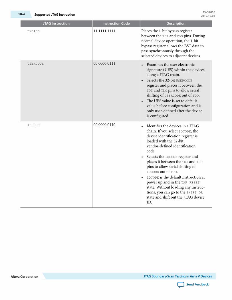
JTAG Instruction Instruction Code Description
BYPASS 11 1111 1111 Places the 1-bit bypass registerbetween the TDI and TDO pins. Duringnormal device operation, the 1-bitbypass register allows the BST data topass synchronously through theselected devices to adjacent devices.
USERCODE 00 0000 0111 • Examines the user electronicsignature (UES) within the devicesalong a JTAG chain.
• Selects the 32-bit USERCODEregister and places it between theTDI and TDO pins to allow serialshifting of USERCODE out of TDO.
• The UES value is set to defaultvalue before configuration and isonly user-defined after the deviceis configured.
IDCODE 00 0000 0110 • Identifies the devices in a JTAGchain. If you select IDCODE, thedevice identification register isloaded with the 32-bitvendor-defined identificationcode.
• Selects the IDCODE register andplaces it between the TDI and TDOpins to allow serial shifting ofIDCODE out of TDO.
• IDCODE is the default instruction atpower up and in the TAP RESETstate. Without loading any instruc‐tions, you can go to the SHIFT_DRstate and shift out the JTAG deviceID.
10-4 Supported JTAG InstructionAV-52010
2019.10.03
Altera Corporation JTAG Boundary-Scan Testing in Arria V Devices
Send Feedback
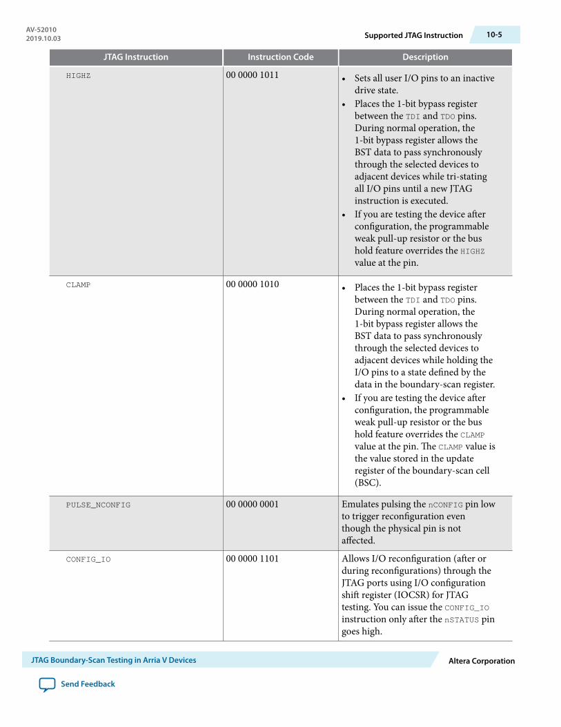
JTAG Instruction Instruction Code Description
HIGHZ 00 0000 1011 • Sets all user I/O pins to an inactivedrive state.
• Places the 1-bit bypass registerbetween the TDI and TDO pins.During normal operation, the1-bit bypass register allows theBST data to pass synchronouslythrough the selected devices toadjacent devices while tri-statingall I/O pins until a new JTAGinstruction is executed.
• If you are testing the device afterconfiguration, the programmableweak pull-up resistor or the bushold feature overrides the HIGHZvalue at the pin.
CLAMP 00 0000 1010 • Places the 1-bit bypass registerbetween the TDI and TDO pins.During normal operation, the1-bit bypass register allows theBST data to pass synchronouslythrough the selected devices toadjacent devices while holding theI/O pins to a state defined by thedata in the boundary-scan register.
• If you are testing the device afterconfiguration, the programmableweak pull-up resistor or the bushold feature overrides the CLAMPvalue at the pin. The CLAMP value isthe value stored in the updateregister of the boundary-scan cell(BSC).
PULSE_NCONFIG 00 0000 0001 Emulates pulsing the nCONFIG pin lowto trigger reconfiguration eventhough the physical pin is notaffected.
CONFIG_IO 00 0000 1101 Allows I/O reconfiguration (after orduring reconfigurations) through theJTAG ports using I/O configurationshift register (IOCSR) for JTAGtesting. You can issue the CONFIG_IOinstruction only after the nSTATUS pingoes high.
AV-520102019.10.03 Supported JTAG Instruction 10-5
JTAG Boundary-Scan Testing in Arria V Devices Altera Corporation
Send Feedback

JTAG Instruction Instruction Code Description
LOCK 01 1111 0000 Put the device in JTAG secure mode.In this mode, only BYPASS, SAMPLE/PRELOAD, EXTEST, IDCODE,SHIFT_EDERROR_REG, and UNLOCKinstructions are supported. Thisinstruction can only be accessedthrough JTAG core access in usermode. It cannot be accessed throughexternal JTAG pins in test or usermode.
UNLOCK 11 0011 0001 Release the device from the JTAGsecure mode to enable access to allother JTAG instructions. This instruc‐tion can only be accessed throughJTAG core access in user mode. Itcannot be accessed through externalJTAG pins in test or user mode.
KEY_CLR_VREG 00 0010 1001 Clears the volatile key.
KEY_VERIFY 00 0001 0011 Verifies the non-volatile key has beencleared.
EXTEST_PULSE (38) 00 1000 1111 Enables board-level connectivitychecking between the transmittersand receivers that are AC coupled bygenerating three output transitions:
• Driver drives data on the fallingedge of TCK in theUPDATE_IR/DR state.
• Driver drives inverted data on thefalling edge of TCK after enteringthe RUN_TEST/IDLE state.
• Driver drives data on the fallingedge of TCK after leaving theRUN_TEST/IDLE state.
The EXTEST_PULSE JTAG instructionis only supported in user mode forArria V GZ devices.
(38) This instruction is only supported by Arria V GZ devices.
10-6 Supported JTAG InstructionAV-52010
2019.10.03
Altera Corporation JTAG Boundary-Scan Testing in Arria V Devices
Send Feedback

JTAG Instruction Instruction Code Description
EXTEST_TRAIN (38) 00 0100 1111 Behaves the same as theEXTEST_PULSE instruction except thatthe output continues to toggle on theTCK falling edge as long as the TAPcontroller is in the RUN_TEST/IDLEstate.
The EXTEST_TRAIN JTAG instructionis only supported in user mode forArria V GZ devices.
Note: If the device is in a reset state and the nCONFIG or nSTATUS signal is low, the device IDCODE mightnot be read correctly. To read the device IDCODE correctly, you must issue the IDCODE JTAG instruc‐tion only when the nCONFIG and nSTATUS signals are high.
Note: If you use DC coupling on HSSI signals, execute the EXTEST instruction. If you use AC coupling onHSSI signals, execute the EXTEST_PULSE instruction. AC-coupled and DC-coupled HSSI are onlysupported in post-configuration mode.
Related InformationJTAG Secure Mode on page 8-45Provides more information about PULSE_NCONFIG, CONFIG_IO, LOCK, and UNLOCK JTAG instructions.
JTAG Secure ModeIf you enable the tamper-protection bit, the Arria V device is in JTAG secure mode after power up. In theJTAG secure mode, the JTAG pins support only the BYPASS, SAMPLE/PRELOAD, EXTEST, IDCODE,SHIFT_EDERROR_REG, and UNLOCK instructions. Issue the UNLOCK JTAG instruction to enable support forother JTAG instructions.
JTAG Private InstructionCaution: Never invoke the following instruction codes. These instructions can damage and render the
device unusable:
• 1100010000• 0011001001• 0000101011(39)
• 1100010111• 1100010011 (40)
• 1010100001• 0101011110• 0000101010
(39) This JTAG private instruction is not applicable for Arria V GZ devices.(40) This JTAG private instruction is only applicable for Arria V GZ devices.
AV-520102019.10.03 JTAG Secure Mode 10-7
JTAG Boundary-Scan Testing in Arria V Devices Altera Corporation
Send Feedback

I/O Voltage for JTAG OperationThe Arria V device operating in IEEE Std. 1149.1 BST mode uses four dedicated JTAG pins—TDI, TDO,TMS, and TCK. Arria V devices do not support the optional TRST pin.
The TCK pin has an internal weak pull-down resistor, while the TDI and TMS pins have internal weak pull-up resistors. The 3.3-, 3.0-, or 2.5-V VCCPD supply of I/O bank 3A powers the TDO, TDI, TMS, and TCK pins.All user I/O pins are tri-stated during JTAG configuration.
The JTAG chain supports several different devices. Use the supported TDO and TDI voltage combinationslisted in the following table if the JTAG chain contains devices that have different VCCIO levels. The outputvoltage level of the TDO pin must meet the specification of the TDI pin it drives.
Note: Arria V GZ devices do not support 3.3-V VCCPD supply.
Table 10-3: Supported TDO and TDI Voltage Combinations
The TDO output buffer for VCCPD of 3.3 V or 3.0 V meets VOH (MIN) of 2.4 V, and the TDO outputbuffer for VCCPD of 2.5 V meets VOH (MIN) of 2.0 V.
Device TDI Input BufferPower (V)
Arria V TDO VCCPD
VCCPD = 3.3 V VCCPD = 3.0 V VCCPD = 2.5 V
Arria V
VCCPD = 3.3 Yes Yes Yes
VCCPD = 3.0 Yes Yes Yes
VCCPD = 2.5 Yes Yes Yes
Non- Arria V(41)
VCC = 3.3 Yes Yes Yes
VCC = 2.5 Yes Yes Yes
VCC = 1.8 Yes Yes Yes
VCC = 1.5 Yes Yes Yes
Performing BSTYou can issue BYPASS, IDCODE, and SAMPLE JTAG instructions before, after, or during configurationwithout having to interrupt configuration.
To issue other JTAG instructions, follow these guidelines:
• To perform testing before configuration, hold the nCONFIG pin low.• To perform BST during configuration, issue CONFIG_IO JTAG instruction to interrupt configuration.
While configuration is interrupted, you can issue other JTAG instructions to perform BST. After BST iscompleted, issue the PULSE_CONFIG JTAG instruction or pulse nCONFIG low to reconfigure the device.
(41) The input buffer must be tolerant to the TDO VCCPD voltage.
10-8 I/O Voltage for JTAG OperationAV-52010
2019.10.03
Altera Corporation JTAG Boundary-Scan Testing in Arria V Devices
Send Feedback

The chip-wide reset (DEV_CLRn) and chip-wide output enable (DEV_OE) pins on Arria V devices do notaffect JTAG boundary-scan or configuration operations. Toggling these pins does not disrupt BSToperation (other than the expected BST behavior).
If you design a board for JTAG configuration of Arria V devices, consider the connections for thededicated configuration pins.
Related Information
• JTAG Configuration on page 8-33Provides more information about JTAG configuration.
• Arria V GT and GX Device Family Pin Connection GuidelinesProvides more information about pin connections.
• Arria V GZ Device Family Pin Connection GuidelinesProvides more information about pin connections.
• Arria V Device DatasheetProvides more information about JTAG configuration timing.
Enabling and Disabling IEEE Std. 1149.1 BST CircuitryThe IEEE Std. 1149.1 BST circuitry is enabled after the Arria V device powers up. However for Arria VSoC FPGAs, you must power up both HPS and FPGA to perform BST.
The HPS should be held in reset while performing BST to stop the I/Os being accessed or setup by theHPS.
To ensure that you do not inadvertently enable the IEEE Std. 1149.1 circuitry when it is not required,disable the circuitry permanently with pin connections as listed in the following table.
Table 10-4: Pin Connections to Permanently Disable the IEEE Std. 1149.1 Circuitry for Arria V Devices
JTAG Pins(42) Connection for Disabling
TMS VCCPD supply of Bank 3A
TCK GND
TDI VCCPD supply of Bank 3A
TDO Leave open
(42) The JTAG pins are dedicated. Software option is not available to disable JTAG in Arria V devices.
AV-520102019.10.03 Enabling and Disabling IEEE Std. 1149.1 BST Circuitry 10-9
JTAG Boundary-Scan Testing in Arria V Devices Altera Corporation
Send Feedback
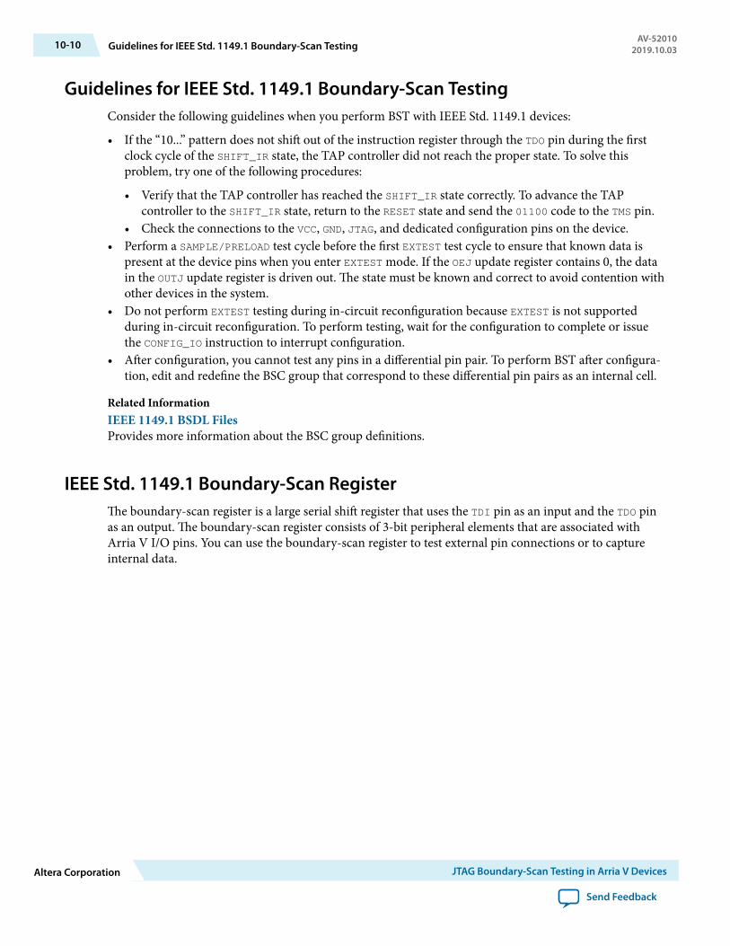
Guidelines for IEEE Std. 1149.1 Boundary-Scan TestingConsider the following guidelines when you perform BST with IEEE Std. 1149.1 devices:
• If the “10...” pattern does not shift out of the instruction register through the TDO pin during the firstclock cycle of the SHIFT_IR state, the TAP controller did not reach the proper state. To solve thisproblem, try one of the following procedures:
• Verify that the TAP controller has reached the SHIFT_IR state correctly. To advance the TAPcontroller to the SHIFT_IR state, return to the RESET state and send the 01100 code to the TMS pin.
• Check the connections to the VCC, GND, JTAG, and dedicated configuration pins on the device.• Perform a SAMPLE/PRELOAD test cycle before the first EXTEST test cycle to ensure that known data is
present at the device pins when you enter EXTEST mode. If the OEJ update register contains 0, the datain the OUTJ update register is driven out. The state must be known and correct to avoid contention withother devices in the system.
• Do not perform EXTEST testing during in-circuit reconfiguration because EXTEST is not supportedduring in-circuit reconfiguration. To perform testing, wait for the configuration to complete or issuethe CONFIG_IO instruction to interrupt configuration.
• After configuration, you cannot test any pins in a differential pin pair. To perform BST after configura‐tion, edit and redefine the BSC group that correspond to these differential pin pairs as an internal cell.
Related InformationIEEE 1149.1 BSDL FilesProvides more information about the BSC group definitions.
IEEE Std. 1149.1 Boundary-Scan RegisterThe boundary-scan register is a large serial shift register that uses the TDI pin as an input and the TDO pinas an output. The boundary-scan register consists of 3-bit peripheral elements that are associated withArria V I/O pins. You can use the boundary-scan register to test external pin connections or to captureinternal data.
10-10 Guidelines for IEEE Std. 1149.1 Boundary-Scan TestingAV-52010
2019.10.03
Altera Corporation JTAG Boundary-Scan Testing in Arria V Devices
Send Feedback
Figure 10-1: Boundary-Scan Register
This figure shows how test data is serially shifted around the periphery of the IEEE Std. 1149.1 device.
TCK TMSTDI TDO
Internal Logic
TAP Controller
Each peripheralelement is either anI/O pin, dedicatedinput pin, or dedicated configuration pin.
Boundary-Scan Cells of an Arria V Device I/O PinThe Arria V device 3-bit BSC consists of the following registers:
• Capture registers—Connect to internal device data through the OUTJ, OEJ, and PIN_IN signals.• Update registers—Connect to external data through the PIN_OUT and PIN_OE signals.
The TAP controller generates the global control signals for the IEEE Std. 1149.1 BST registers (shift,clock, and update) internally. A decode of the instruction register generates the MODE signal.
The data signal path for the boundary-scan register runs from the serial data in (SDI) signal to the serialdata out (SDO) signal. The scan register begins at the TDI pin and ends at the TDO pin of the device.
AV-520102019.10.03 Boundary-Scan Cells of an Arria V Device I/O Pin 10-11
JTAG Boundary-Scan Testing in Arria V Devices Altera Corporation
Send Feedback

Figure 10-2: User I/O BSC with IEEE Std. 1149.1 BST Circuitry for Arria V Devices
01
OUTPUT
OE
INPUTINPUT
OUTPUT
OE
From orTo Device
I/O CellCircuitryAnd/Or
LogicArray
01
010
1
010
1
01
PIN_OUT
INJ
OEJ
OUTJ
VCC
SDO
Pin
SHIFT
SDI
CLOCK HIGHZ MODE
PIN_OE
PIN_IN
OutputBuffer
CaptureRegisters
UpdateRegisters
GlobalSignals
UPDATE
D Q
D Q
D Q D Q
D Q
D Q
Note: TDI, TDO, TMS, and TCK pins, all VCC and GND pin types, and VREF pins do not have BSCs.
Table 10-5: Boundary-Scan Cell Descriptions for Arria V Devices
This table lists the capture and update register capabilities of all BSCs within Arria V devices.
Pin Type
Captures Drives
CommentsOutputCaptureRegister
OE CaptureRegister
InputCaptureRegister
OutputUpdateRegister
OE UpdateRegister
InputUpdateRegister
User I/O pins OUTJ OEJ PIN_IN PIN_OUT PIN_OE INJ —
Dedicatedclock input
0 1 PIN_IN NoConnect(N.C.)
N.C. N.C. PIN_IN drivesto the clocknetwork orlogic array
10-12 Boundary-Scan Cells of an Arria V Device I/O PinAV-52010
2019.10.03
Altera Corporation JTAG Boundary-Scan Testing in Arria V Devices
Send Feedback

Pin Type
Captures Drives
CommentsOutputCaptureRegister
OE CaptureRegister
InputCaptureRegister
OutputUpdateRegister
OE UpdateRegister
InputUpdateRegister
Dedicatedinput(43)
0 1 PIN_IN N.C. N.C. N.C. PIN_IN drivesto the controllogic
Dedicatedbidirectional(open drain)(44)
0 OEJ PIN_IN N.C. N.C. N.C. PIN_IN drivesto theconfigurationcontrol
Dedicatedbidirec‐tional(45)
OUTJ OEJ PIN_IN N.C. N.C. N.C. PIN_IN drivesto theconfigurationcontrol andOUTJ drives tothe outputbuffer
Dedicatedoutput(46)
OUTJ 0 0 N.C. N.C. N.C. OUTJ drives tothe outputbuffer
IEEE Std. 1149.6 Boundary-Scan Register
The BSCs for HSSI transmitters (GXB_TX[p,n]) and receivers/input clock buffers(GXB_RX[p,n])/(REFCLK[p,n]) in Arria V GZ devices are different from the BSCs for the I/O pins.
(43) This includes the nCONFIG, MSEL0, MSEL1, MSEL2, MSEL3, MSEL4, and nCE pins.(44) This includes the CONF_DONE and nSTATUS pins.(45) This includes the DCLK pin.(46) This includes the nCEO pin.
AV-520102019.10.03 IEEE Std. 1149.6 Boundary-Scan Register 10-13
JTAG Boundary-Scan Testing in Arria V Devices Altera Corporation
Send Feedback

Figure 10-3: HSSI Transmitter BSC with IEEE Std. 1149.6 BST Circuitry for Arria V GZ Devices
MEM_INIT SDIN SHIFT
0
1
0
1
D Q
D Q
CLK
SDOU
T
MODE
AC_TEST AC_MODE
CaptureRegisters
UpdateRegisters
BSTX1
Tx OutputBuffer
0
1
D Q
D Q
D Q
D Q
HIGHZUPDATE
BSCAN PMA
0
1
0
1
0
1BSOEB
MORHZ
OE Logic
BSTX0 OE
OE
nOE
Mission
(DATAOUT)
TX_BUF_OE
ACJTAG_BUF_OE
AC JTAGOutput Buffer
AC JTAGOutput Buffer
Pad
Pad
Figure 10-4: HSSI Receiver/Input Clock Buffer with IEEE Std. 1149.6 BST Circuitry for Arria V GZ Devices
HIGHZ SDIN SHIFT
0
1
0
1
D Q
D Q
CLK
SDOU
T
MODE
AC_TEST
CaptureRegisters
UpdateRegisters
BSRX1
BSOUT1
BSRX0
BSOUT0
MEM_INIT
AC_MODE
BSCAN PMA
UPDATE
HystereticMemory
HystereticMemory
AC JTAG TestReceiver
Mission (DATAIN)Optional INTEST/RUNBISTnot supported
RX InputBuffer
Pad
Pad
AC JTAG TestReceiver
10-14 IEEE Std. 1149.6 Boundary-Scan RegisterAV-52010
2019.10.03
Altera Corporation JTAG Boundary-Scan Testing in Arria V Devices
Send Feedback
JTAG Boundary-Scan Testing inArria V Devices Revision History
Date Version Changes
June 2016 2016.06.10 Added 0000101010 instruction code into JTAG Private Instructionsection.
December2015
2015.12.21 Changed instances of Quartus II to Quartus Prime.
June 2015 2015.06.12 Added a note in the Enabling and Disabling IEEE Std. 1149.1 BSTCircuitry section.
June 2014 2014.06.30 Removed a note in the Performing BST section.
January 2014 2014.01.10 • Added a note to the Performing BST section.• Updated the Supported JTAG Instruction section.• Updated the KEY_CLR_VREG JTAG instruction.
May 2013 2013.05.06 • Added link to the known document issues in the Knowledge Base.• Updated the description for EXTEST_TRAIN and EXTEST_PULSE JTAG
instructions.• Moved all links to the Related Information section of respective topics
for easy reference.
November2012
2012.11.19 • Added IDCODE for Arria V GZ devices.• Added EXTEST_PULSE and EXTEST_TRAIN JTAG instructions for
Arria V GZ devices.• Added the IEEE Std. 1149.6 Boundary-Scan Register section for
Arria V GZ devices.• Reorganized content and updated template.
June 2012 2.0 • Restructured the chapter.• Updated Table 10-1 and Table 10-2.
February 2012 1.2 Updated Table 10-2.
November2011
1.1 Minor text edits.
May 2011 1.0 Initial release.
AV-520102019.10.03 JTAG Boundary-Scan Testing inArria V Devices Revision History 10-15
JTAG Boundary-Scan Testing in Arria V Devices Altera Corporation
Send Feedback

Power Management in Arria V Devices 112019.10.03
AV-52011 Subscribe Send Feedback
This chapter describes the hot-socketing feature, power-on reset (POR) requirements, power-upsequencing recommendation, temperature sensing diode (TSD), and their implementation in Arria Vdevices.
Related Information
• Arria V Device Handbook: Known IssuesLists the planned updates to the Arria V Device Handbook chapters.
• PowerPlay Power AnalysisProvides more information about the Quartus®II PowerPlay Power Analyzer tool in volume 3 of theQuartus II Handbook.
• Arria V Device DatasheetProvides more information about the recommended operating conditions of each power supply.
• Arria V GT and GX Device Family Pin Connection GuidelinesProvides more detailed information about power supply pin connection guidelines and powerregulator sharing.
• Arria V GZ Device Family Pin Connection GuidelinesProvides more detailed information about power supply pin connection guidelines and powerregulator sharing.
• Board Design Resource CenterProvides more detailed information about power supply design requirements.
• Arria V and Cyclone V Design Guidelines
Power ConsumptionThe total power consumption of an Arria V device consists of the following components:
• Static power—the power that the configured device consumes when powered up but no clocks areoperating.
• Dynamic power— the additional power consumption of the device due to signal activity or toggling.
Intel Corporation. All rights reserved. Intel, the Intel logo, Altera, Arria, Cyclone, Enpirion, MAX, Nios, Quartus and Stratix words and logos are trademarks ofIntel Corporation or its subsidiaries in the U.S. and/or other countries. Intel warrants performance of its FPGA and semiconductor products to currentspecifications in accordance with Intel's standard warranty, but reserves the right to make changes to any products and services at any time without notice.Intel assumes no responsibility or liability arising out of the application or use of any information, product, or service described herein except as expresslyagreed to in writing by Intel. Intel customers are advised to obtain the latest version of device specifications before relying on any published informationand before placing orders for products or services.*Other names and brands may be claimed as the property of others.
ISO9001:2015Registered
www.altera.com101 Innovation Drive, San Jose, CA 95134

Dynamic Power EquationFigure 11-1: Dynamic Power
The following equation shows how to calculate dynamic power where P is power, C is the load capacitance,and V is the supply voltage level.
The equation shows that power is design-dependent and is determined by the operating frequency of yourdesign. Arria V devices minimize static and dynamic power using advanced process optimizations. Thistechnology allows Arria V designs to meet specific performance requirements with the lowest possiblepower.
Programmable Power Technology
Arria V GZ devices offer the ability to configure portions of the core, called tiles, for high-speed or low-power mode of operation performed by the Intel Quartus Prime software without user intervention.Setting a tile to high-speed or low-power mode is accomplished with on-chip circuitry and does notrequire extra power supplies brought into the Arria V GZ device. In a design compilation, the IntelQuartus Prime software determines whether a tile should be in high-speed or low-power mode based onthe timing constraints of the design.
Arria VGZ tiles consist of the following:
• Memory logic array block (MLAB)/ logic array block (LAB) pairs with routing to the pair• MLAB/LAB pairs with routing to the pair and to adjacent digital signal processing (DSP)/ memory
block routing• TriMatrix memory blocks• DSP blocks• PCI Express® (PCIe®) hard IP• Physical coding sublayer (PCS)
All blocks and routing associated with the tile share the same setting of either high-speed or low-powermode. By default, tiles that include DSP blocks or memory blocks are set to high-speed mode for optimumperformance. Unused DSP blocks and memory blocks are set to low-power mode to minimize staticpower. Clock networks do not support programmable power technology.
With programmable power technology, faster speed grade FPGAs may require less power because thereare fewer high-speed MLAB and LAB pairs, when compared with slower speed grade FPGAs. The slowerspeed grade device may have to use more high-speed MLAB and LAB pairs to meet performance require‐ments.
11-2 Dynamic Power EquationAV-52011
2019.10.03
Altera Corporation Power Management in Arria V Devices
Send Feedback
The Intel Quartus Prime software sets unused device resources in the design to low-power mode to reducethe static power. It also sets the following resources to low-power mode when they are not used in thedesign:
• LABs and MLABs• TriMatrix memory blocks• DSP blocks
If a phase-locked loop (PLL) is instantiated in the design, you may assert the areset pin high to keep thePLL in low-power mode.
Altera recommends that you power down unused PCIe HIPs, per side, by connecting the PCIe HIP powerto GND on the PCB for additional power savings. All of the HIPs on a side of the device must be unusedto be powered down. For additional information refer to the pin connection guidelines.
Table 11-1: Programmable Power Capabilities for Arria V GZ Devices
This table lists the available Arria V GZ programmable power capabilities. Speed grade considerations canadd to the permutations to give you flexibility in designing your system.
Feature Programmable Power Technology
LAB Yes
Routing Yes
Memory Blocks Fixed setting(47)
DSP Blocks Fixed setting(47)
Clock Networks No
Related Information
• Arria V GT and GX Device Family Pin Connection GuidelinesProvides more information about powering down PCIe HIPs.
• Arria V GZ Device Family Pin Connection Guidelines.Provides more information about powering down PCIe HIPs.
Temperature Sensing Diode
The Arria V TSD uses the characteristics of a PN junction diode to determine die temperature. Knowingthe junction temperature is crucial for thermal management. You can calculate junction temperature usingambient or case temperature, junction-to-ambient (ja) or junction-to-case (jc) thermal resistance, anddevice power consumption. Arria V devices monitor its die temperature with the internal TSD withbuilt-in analog-to-digital converter (ADC) circuitry or the external TSD with an external temperaturesensor. This allows you to control the air flow to the device.
All Arria V devices support internal TSD only except for Arria V GZ devices that support both internaland external TSDs.
(47) Tiles with DSP blocks and memory blocks that are used in the design are always set to high-speed mode. Bydefault, unused DSP blocks and memory blocks are set to low-power mode.
AV-520112019.10.03 Temperature Sensing Diode 11-3
Power Management in Arria V Devices Altera Corporation
Send Feedback

Internal Temperature Sensing DiodeYou can use the Arria V internal TSD in the following operations:
• Power-up mode—to read the die's temperature during configuration, enable the Altera TemperatureSensor IP core in your design.
• User mode—to read the die's temperature during user mode, assert the clken signal to the internalTSD circuitry.
Note: To reduce power consumption, disable the Arria V internal TSD when you are not using it.
Related Information
• Altera Temperature Sensor IP Core User GuideProvides more information about using the Altera Temperature Sensor IP core.
• Arria V Device DatasheetProvides more information about the Arria V internal TSD specification.
External Temperature Sensing Diode
The Arria V GZ external TSD requires two pins for voltage reference. The following figure shows how toconnect the external TSD with an external temperature sensor device, allowing external sensing of theArria V GZ die temperature. For example, you can connect external temperature sensing devices, such asMAX1619, MAX1617A, MAX6627, and ADT7411 to the two external TSD pins for Arria V GZ device dietemperature reading. The TSD diode is a substrate or common collector PNP diode type.
Figure 11-2: TSD External Pin Connections
FPGA
TEMPDIODEPExternal TSD
TEMPDIODEN
External Temperature Sensor
The TSD is a very sensitive circuit that can be influenced by noise coupled from other traces on the boardor within the device package itself, depending on your device usage. The interfacing signal from theArria V GZ device to the external temperature sensor is based on millivolts (mV) of difference, as seen atthe external TSD pins. Switching the I/O near the TSD pins can affect the temperature reading. Alterarecommends taking temperature readings during periods of inactivity in the device or use the internalTSD with built-in ADC circuitry.
11-4 Internal Temperature Sensing DiodeAV-52011
2019.10.03
Altera Corporation Power Management in Arria V Devices
Send Feedback
The following are board connection guidelines for the TSD external pin connections:
• The maximum trace lengths for the TEMPDIODEP/TEMPDIODEN traces must be less than eightinches.
• Route both traces in parallel and place them close to each other with grounded guard tracks on eachside.
• Altera recommends 10-mils width and space for both traces.• Route traces through a minimum number of vias and crossunders to minimize the thermocouple
effects.• Ensure that the number of vias are the same on both traces.• Ensure both traces are approximately the same length.• Avoid coupling with toggling signals (for example, clocks and I/O) by having the GND plane between
the diode traces and the high frequency signals.• For high-frequency noise filtering, place an external capacitor (close to the external chip) between the
TEMPDIODEP/TEMPDIODEN trace. For Maxim devices, use an external capacitor between 2200 pFto 3300 pF.
• Place a 0.1 uF bypass capacitor close to the external device.• You can use the internal TSD with built-in ADC circuitry and external TSD at the same time.• If you only use internal ADC circuitry, the external TSD pins (TEMPDIODEP/TEMPDIODEN) can be
connected to GND because the external TSD pins are not used.
For details about device specification and connection guidelines, refer to the external temperature sensordevice datasheet from the device manufacturer.
Related Information
• Arria V Device DatasheetProvides more information about the external TSD specification.
• Arria V GT and GX Device Family Pin Connection GuidelinesProvides details about the TEMPDIODEP/TEMPDIODEN pin connection when you are not using anexternal TSD.
• Arria V GZ Device Family Pin Connection Guidelines.Provides details about the TEMPDIODEP/TEMPDIODEN pin connection when you are not using anexternal TSD.
Hot-Socketing FeatureArria V devices support hot socketing—also known as hot plug-in or hot swap.
The hot-socketing circuitry monitors the following power supplies and banks:
• Arria V GX, GT, SX, and ST devices—VCCIO, VCCPD, VCC, and VCCP power supplies and all VCCIO andVCCPD banks.
• Arria V GZ devices—VCCIO, VCCPD, and VCC power supplies and all VCCIO and VCCPD banks.
When powering up or powering down these power supplies, refer to the Power-Up Sequence section ofthis handbook.
During the hot-socketing operation, the I/O pin capacitance is less than 15 pF and the clock pincapacitance is less than 20 pF.
AV-520112019.10.03 Hot-Socketing Feature 11-5
Power Management in Arria V Devices Altera Corporation
Send Feedback

The hot-socketing capability removes some of the difficulty that designers face when using the Arria Vdevices on PCBs that contain a mixture of devices with different voltage requirements.
The hot-socketing capability in Arria V devices provides the following advantages:
• You can drive signals into the I/O, dedicated input, and dedicated clock pins before or during power upor power down without damaging the device. External input signals to the I/O pins of the unpowereddevice will not power the power supplies through internal paths within the device.
• The output buffers are tri-stated during system power up or power down. Because the Arria V devicedoes not drive signals out before or during power up, the device does not affect the other operatingbuses.
• You can insert or remove an Arria V device from a powered-up system board without damaging orinterfering with the system board's operation. This capability allows you to avoid sinking currentthrough the device signal pins to the device power supply, which can create a direct connection toGND that causes power supply failures.
• During hot socketing, Arria V devices are immune to latch up that can occur when a device is hot-socketed into an active system.
Altera uses GND as a reference for hot-socketing and I/O buffer circuitry designs. To ensure properoperation, connect GND between boards before connecting the power supplies. This prevents GND onyour board from being pulled up inadvertently by a path to power through other components on yourboard. A pulled up GND could otherwise cause an out-of-specification I/O voltage or over currentcondition in the Altera device.
Related Information
• Arria V GX, GT, SX, and ST Power-Up Sequence on page 11-7• Arria V GZ Power-Up Sequence on page 11-9• Arria V Device Datasheet
Provides details about the Arria V hot-socketing specifications.
Hot-Socketing ImplementationThe hot-socketing feature tri-state the output buffer during power up and power down of the powersupplies. When these power supplies are below the threshold voltage, the hot-socketing circuitry generatesan internal HOTSCKT signal.
Hot-socketing circuitry prevents excess I/O leakage during power up. When the voltage ramps up veryslowly, I/O leakage is still relatively low, even after the release of the POR signal and configuration iscomplete.
Note: The output buffer cannot flip from the state set by the hot-socketing circuitry at very low voltage. Toallow the CONF_DONE and nSTATUS pins to operate during configuration, the hot-socketing featureis not applied to these configuration pins. Therefore, these pins will drive out during power up andpower down.
11-6 Hot-Socketing ImplementationAV-52011
2019.10.03
Altera Corporation Power Management in Arria V Devices
Send Feedback

Figure 11-3: Hot-Socketing Circuitry for Arria V Devices
V CCIO
PAD
R
VoltageTolerance
Control
Output Enable
Hot-Socket
OutputPre-Driver
Power-OnReset (POR)
Monitor
WeakPull-Up
Resistor
Input Bufferto Logic Array
The POR circuitry monitors the voltage level of the power supplies and keeps the I/O pins tri-stated untilthe device is in user mode. The weak pull-up resistor (R) in the Arria V input/output element (IOE) isenabled during configuration download to keep the I/O pins from floating.
The 3.3-V tolerance control circuit allows the I/O pins to be driven by 3.3 V before the power supplies arepowered and prevents the I/O pins from driving out before the device enters user mode.
Arria V GX, GT, SX, and ST Power-Up SequenceCaution: To ensure minimum current consumption during power up, and to avoid functionality issue,
follow the power-up sequence shown in the following figure. This power-up sequence isrequired for all Arria V GX and GT devices, except Arria V GX A5 and A7, and Arria V GT C7devices. However, to ensure minimum current consumption during power up, Alterarecommends that you also follow the power-up sequence for the Arria V GX A5 and A7, andArria VGT C7 devices.
Note: If you plan to migrate your design from Arria V GX A5 and A7, and Arria V GT C7 devices toother Arria V devices, your design must adhere to the power-up sequence required for the otherArria V devices.
AV-520112019.10.03 Arria V GX, GT, SX, and ST Power-Up Sequence 11-7
Power Management in Arria V Devices Altera Corporation
Send Feedback

Figure 11-4: Power-Up Sequence Requirement for Arria V GX and GT DevicesPower up VCCBAT at any time. Ramp up the power rails in each group to a minimum of 80% of their fullrail before the next group starts. Power up VCCP, VCCR_GXB, VCCT_GXB, and VCCL_GXB together with VCC.
Group 1
V CCV CCPV CCR_GXBV CCT_GXBV CCL_GXB
Group 2
V CCPGMV CCIOV CCPDV CCA_FPLLV CCA_GXBV CC_AUX
Group 3
V CCD_FPLLV CCH_GXB
Figure 11-5: Power-Up Sequence Recommendation for Arria V SX and ST Devices
Power up the Vccbat at any time. Ramp up the power rails in each group to a minimum of 80% of theirrecommended operating range before the next group starts.
Group 1
VCCVCCPVCCR_GXBVCCT_GXBVCCL_GXBVCC_HPS
Group 2VCCPGMVCCIOVCCPDVCCA_FPLLVCCA_GXBVCC_AUXVCCPD_HPSVCCIO_HPSVCCRSTCLK_HPSVCCPLL_HPSVCC_AUX_SHARED
Group 3
V CCD_FPLLV CCH_GXB
Table 11-2 lists the current transient that you may observe at the indicated power rails after powering upthe Arria V device, and before configuration starts. These transients have a finite duration bounded by thetime at which the device enters configuration mode. For Arria V SX and ST devices, you may observe thecurrent transient in Table 11-2 after powering up the device, and before all the power supplies reach therecommended operating range.
11-8 Arria V GX, GT, SX, and ST Power-Up SequenceAV-52011
2019.10.03
Altera Corporation Power Management in Arria V Devices
Send Feedback

Table 11-2: Maximum Power Supply Current Transient and Typical Duration
Power Rail Maximum Power SupplyCurrent Transient (mA)
Typical Duration (µs) (48)
VCCPD(49), (50) 1250 50
VCCIO(50), (51) 350 200
VCC_AUX(52) 450 10
VCC(52) 700 100
VCCPD_HPS(53), (54), (55) 400 50
VCCIO_HPS(53), (56), (55) 100 200
VCC_HPS(52), (53) 420 100
For details about the minimum current requirements, refer to the Early Power Estimator (EPE), andcompare to the information listed in Table 11-2. If the current transient exceeds the minimum currentrequirements in the EPE, you need to take the information into consideration for your power regulatordesign.
Related InformationPowerPlay Early Power Estimators (EPE) and Power AnalyzerProvides more information about the PowerPlay EPE support for Arria V devices.
Arria V GZ Power-Up Sequence
The Arria V GZ devices require a power-up sequence as shown in the following figure to prevent excessiveinrush current and ensure proper transceiver functionality. This power-up sequence is divided into fourpower groups. Group 1 contains the first power rails to ramp. The VCC, VCCHIP, and VCCHSSI power railsin this group must ramp to a minimum of 80% of their full rail before any other power rails may start.Group 1 power rails can continue to ramp to full rail. The power rails in Group 2 and Group 4 can start toramp in any order after Group 1 has reached its minimum 80% threshold. When the last power rail in
(48) Only typical duration is provided as it may vary on the board design.(49) You may observe the current transient at VCCPD only when you do not follow the recommended power-up
sequence. To avoid the current transient at VCCPD, follow the recommended power-up sequence.(50) The maximum current for VCCIO and VCCPD applies to all voltage levels supported by the Arria V device.(51) You may observe the current transient at VCCIO if you power up VCCIO before VCCPD. To avoid the current
transient at VCCIO, follow the recommended power-up sequence by powering up VCCIO and VCCPD together.(52) You may observe the current transient at VCC_AUX, VCC and VCC_HPS with any power-up sequence.(53) These power rails are only available on Arria V SX and ST devices.(54) You may observe the current transient at VCCPD_HPS only when you do not follow the recommended power-
up sequence. To avoid the current transient at VCCPD_HPS, follow the recommended power-up sequence.(55) The maximum current for VCCIO_HPS and VCCPD_HPS applies to all voltage levels supported by the Arria V
device.(56) You may observe the current transient at VCCIO_HPS if you power up VCCIO_HPS before VCCPD_HPS. To avoid
the current transient at VCCIO_HPS, follow the recommended power-up sequence by powering up VCCIO_HPSand VCCPD_HPS together.
AV-520112019.10.03 Arria V GZ Power-Up Sequence 11-9
Power Management in Arria V Devices Altera Corporation
Send Feedback
Group 2 reaches 80% of its full rail, the remaining power rails in Group 3 may start their ramp. Duringthis time, Group 2 power rails may continue to ramp to full rail. Power rails in Group 3 may ramp in anyorder. All power rails must ramp monotonically. The complete power-up sequence must meet either thestandard or fast POR delay time, depending on the POR delay setting that is used.
Figure 11-6: Power-Up Sequence Requirement for Arria V GZ Devices
Power up VCCBAT at any time. If VCC, VCCR_GXB, and VCCT_GXB have the same voltage level, they can bepowered by the same regulator in Group 1 and ramp simultaneously.
V CCPTV CCH_GXBV CCD_FPLLV CCT_GXBV CCR_GXB
V CCIO
V CCPDV CCPGMV CCA_FPLLV CC_AUXV CCA_GXB
V CCV CCHIPV CCHSSI
Group 1 Group 2 Group 3
80% of Last Rail in Group 2
Group 4
80% V CC
Group 3
Group 4
Group 2
Group 1
Arria V GZ devices may power down all power rails simultaneously. However, all rails must reach 0 Vwithin 100 ms from the start of power-down.
11-10 Arria V GZ Power-Up SequenceAV-52011
2019.10.03
Altera Corporation Power Management in Arria V Devices
Send Feedback
Power-On Reset CircuitryThe POR circuitry keeps the Arria V device in the reset state until the power supply outputs are within therecommended operating range.
A POR event occurs when you power up the Arria V device until the power supplies reach therecommended operating range within the maximum power supply ramp time, tRAMP. If tRAMP is not met,the Arria V device I/O pins and programming registers remain tri-stated, during which device configura‐tion could fail.
Figure 11-7: Relationship Between tRAMP and POR Delay
Time
POR trip level
Volts
POR delay configuration timetRAMP
first power supply
last power supply
The Arria V POR circuitry uses an individual detecting circuitry to monitor each of theconfiguration-related power supplies independently. The main POR circuitry is gated by the outputs of allthe individual detectors. The main POR signal is asserted when the power starts to ramp up. This signal isreleased after the last ramp-up power reaches the POR trip level during power up.
In user mode, the main POR signal is asserted when any of the monitored power goes below its POR triplevel. Asserting the POR signal forces the device into the reset state.
The POR circuitry checks the functionality of the I/O level shifters powered by the VCCPD and VCCPGMpower supplies during power-up mode. The main POR circuitry waits for all the individual PORcircuitries to release the POR signal before allowing the control block to start programming the device.
AV-520112019.10.03 Power-On Reset Circuitry 11-11
Power Management in Arria V Devices Altera Corporation
Send Feedback

Figure 11-8: Simplified POR Diagram for Arria V Devices
V CC
ModularMain POR
Main PORV CC_AUX
V CCPDV CCPGM
V CC POR
V CCP V CCP POR
V CC_AUX POR
Related InformationArria V Device DatasheetProvides more information about the POR delay specification and tRAMP.
Power Supplies Monitored and Not Monitored by the POR Circuitry
Table 11-3: Power Supplies Monitored and Not Monitored by the Arria V POR Circuitry
Devices Power SuppliesMonitored
Power Supplies Not Monitored
Arria VGX and GT
• VCC_AUX• VCCBAT• VCC• VCCP• VCCPD• VCCPGM
• VCCT_GXB• VCCH_GXB• VCCR_GXB• VCCA_GXB• VCCL_GXB• VCCA_FPLL• VCCD_FPLL• VCCIO
Arria V GZ • VCC_AUX• VCCBAT• VCC• VCCPT• VCCPD• VCCPGM
• VCCT_GXB• VCCH_GXB• VCCR_GXB• VCCA_GXB• VCCA_FPLL• VCCD_FPLL• VCCIO• VCCHIP
11-12 Power Supplies Monitored and Not Monitored by the POR CircuitryAV-52011
2019.10.03
Altera Corporation Power Management in Arria V Devices
Send Feedback
Devices Power SuppliesMonitored
Power Supplies Not Monitored
Arria VSX and ST
• VCC_AUX• VCCBAT• VCC• VCCP• VCCPD• VCCPGM• VCC_HPS• VCCPD_HPS• VCCRSTCLK_HPS• VCC_AUX_SHARED
• VCCT_GXB• VCCH_GXB• VCCR_GXB• VCCA_GXB• VCCL_GXB• VCCA_FPLL• VCCD_FPLL• VCCIO• VCCIO_HPS• VCCPLL_HPS
Note: For the device to exit POR, you must power the VCCBAT power supply even if you do not use thevolatile key.
Related InformationMSEL Pin SettingsProvides information about the MSEL pin settings for each POR delay.
Power Management in Arria V Devices Revision History
Date Version Changes
December2015
2015.12.21 • Changed instances of Quartus II to Quartus Prime.• Updated the External Temperature Sensing Diode section to provide
the type of diode used.• Updated the Arria V GZ Power-Up Sequence section.
January 2015 2015.01.23 • Added VCC_AUX_SHARED to the power supplies monitored by the ArriaV POR circuitry for Arria V SX and ST devices.
• Added a link to the Arria V and Cyclone V Design Guidelines.
January 2014 2014.01.10 Updated the note to the VCCPD_HPS power rail that current transient atVCCPD_HPS is observed only when the recommended power-up sequenceis not followed. To avoid the current transient at VCCPD_HPS, follow therecommended power-up sequence.
June 2013 2013.06.28 • Added power-up sequences for Arria V SX and ST devices.• Added the current transient that occurs on HPS power rails during
power-up
AV-520112019.10.03 Power Management in Arria V Devices Revision History 11-13
Power Management in Arria V Devices Altera Corporation
Send Feedback
Date Version Changes
May 2013 2013.05.06 • Added link to the known document issues in the Knowledge Base.• Moved all links to the Related Information section of respective topics
for easy reference.• Updated dynamic power in Power Consumption for improve clarity.• Added description on powering down unused PCIe HIPS in
Programmable Power Technology• Updated Hot-Socketing Feature with 'When powering up these power
supplies, refer to the Power-Up Sequence section of this handbook.'• Updated description about power-up sequence requirement for device
migration to improve clarity.• Updated Figure 11-5 by renaming VCCA_GXB/GTB, VCCT_GXB/GTB,
VCCR_GXB/GTB to VCCA_GXB, VCCT_GXB, VCCR_GXB and deletingVCCL_GTB.
January 2013 2013.01.11 Updated the power-up sequence for Arria V GX and GT devices.
November2012
2012.11.19 • Added the Programmable Power Technology section for Arria V GZdevices.
• Added the External TSD section for Arria V GZ devices.• Added the Power-up sequence section for Arria V GZ devices.• Added the power supplies monitored and not monitored by the
Arria V GZ devices.• Reorganized content and updated template.
June 2012 2.1 Updated the "Power-Up Sequence" section.
June 2012 2.0 • Restructured the chapter.• Added the "Power-Up Sequencing" section.
February 2012 1.3 Updated VCCP description.
December2011
1.2 • Added VCCP information.• Updated Table 11-1.
November2011
1.1 Restructured chapter.
May 2011 1.0 Initial release.
11-14 Power Management in Arria V Devices Revision HistoryAV-52011
2019.10.03
Altera Corporation Power Management in Arria V Devices
Send Feedback


