Nuclear Instruments and Methods in Physics Research A 583 (2007) 302–312 The high resolution array (HiRA) for rare isotope beam experiments $ M.S. Wallace a, ,1 , M.A. Famiano a,b , M.-J. van Goethem a , A.M. Rogers a , W.G. Lynch a , J. Clifford a , F. Delaunay a , J. Lee a , S. Labostov a , M. Mocko a , L. Morris a , A. Moroni e , B.E. Nett a , D.J. Oostdyk a , R. Krishnasamy a , M.B. Tsang a , R.T. de Souza c , S. Hudan c , L.G. Sobotka d , R.J. Charity d , J. Elson d , G.L. Engel f a National Superconducting Cyclotron Laboratory and Department of Physics and Astronomy, Michigan State University, East Lansing, MI 48824, USA b Department of Physics, Western Michigan University, Kalamazoo, MI 49008, USA c Indiana University Cyclotron Facility and Department of Chemistry, Indiana University, Bloomington, IN 47405, USA d Department of Chemistry, Washington University, St. Louis, MO 63130, USA e INFN, Milano, Italy f Department of Electrical and Computer Engineering, VLSI Design Research Laboratory, Southern Illinois University Edwardsville, IL 62025, USA Received 12 March 2007; received in revised form 21 July 2007; accepted 29 August 2007 Available online 19 September 2007 Abstract The High Resolution Array (HiRA) is a large solid-angle array of silicon strip-detectors that has been developed for use in a variety of nuclear structure, nuclear astrophysics and nuclear reaction experiments with short lived beta-unstable beams. It consists of 20 identical telescopes each composed of a thin ð65 mmÞ single-sided silicon strip-detector, a thick (1.5 mm) double-sided silicon strip-detector, and four CsI(Tl) crystals read out by photodiodes. The array can be easily configured to meet the detection requirements of specific experiments. To process the signals from the 1920 strips in the array, an Application Specific Integrated Circuit (ASIC) was developed. The design and performance characteristics of HiRA are described. r 2007 Elsevier B.V. All rights reserved. PACS: 29.40.Wk; 28.41.Rc Keywords: Charged particle detection; Silicon detectors; Silicon strip-detectors 1. Introduction The development of unstable rare isotope beams at laboratories such as the NSCL [1], RIKEN [2], GANIL [3] and GSI [4] now permits the study of nuclei far from the valley of beta stability. Experiments with rare isotope beams elucidate the structure of both very neutron-rich and neutron-deficient nuclei and clarify which reactions contribute meaningfully to the nucleo-synthetic r-process or rp-processes within hot or explosive astrophysical environments. Experiments in such facilities will provide meaningful constraints on the isospin dependent interac- tions within neutron-rich nuclei and neutron stars. Many of these experiments require reactions to be induced by the most neutron-rich or neutron-deficient isotopes available. Even at the most advanced rare isotope facilities, the available beam intensities for these exotic nuclei are low. To investigate reactions with such beams, it is critical to use a detection system that efficiently covers most, if not all of the interesting kinematically allowable space. The location, in the lab frame, where particles are emitted depends strongly on the reaction mechanism. A variety of silicon strip arrays have been developed to address such needs [5–8]. At low incident energies, where particles may stop in a relatively thin silicon strip-detector, devices such as TIARA [5], which consists of a single layer ARTICLE IN PRESS www.elsevier.com/locate/nima 0168-9002/$ - see front matter r 2007 Elsevier B.V. All rights reserved. doi:10.1016/j.nima.2007.08.248 $ This work is supported by the National Science Foundation under Grant nos. PHY-01-10253, PHY-9977707 and by the DOE under grant nos. DE-FG02-87ER-40316 and DE-FG02-88ER-40404. Corresponding author. Tel.: +1 505 667 3700; fax: +1 505 665 4414. E-mail address: [email protected] (M.S. Wallace). 1 Now with Los Alamos National Laboratory.
Transcript
ARTICLE IN PRESS
0168-9002/$ - se
doi:10.1016/j.ni
$This work
Grant nos. PH
nos. DE-FG02-�CorrespondE-mail addr
1Now with L
Nuclear Instruments and Methods in Physics Research A 583 (2007) 302–312
www.elsevier.com/locate/nima
The high resolution array (HiRA) for rare isotope beam experiments$
M.S. Wallacea,�,1, M.A. Famianoa,b, M.-J. van Goethema, A.M. Rogersa, W.G. Lyncha,J. Clifforda, F. Delaunaya, J. Leea, S. Labostova, M. Mockoa, L. Morrisa, A. Moronie,B.E. Netta, D.J. Oostdyka, R. Krishnasamya, M.B. Tsanga, R.T. de Souzac, S. Hudanc,
L.G. Sobotkad, R.J. Charityd, J. Elsond, G.L. Engelf
aNational Superconducting Cyclotron Laboratory and Department of Physics and Astronomy, Michigan State University, East Lansing, MI 48824, USAbDepartment of Physics, Western Michigan University, Kalamazoo, MI 49008, USA
cIndiana University Cyclotron Facility and Department of Chemistry, Indiana University, Bloomington, IN 47405, USAdDepartment of Chemistry, Washington University, St. Louis, MO 63130, USA
eINFN, Milano, ItalyfDepartment of Electrical and Computer Engineering, VLSI Design Research Laboratory, Southern Illinois University Edwardsville, IL 62025, USA
Received 12 March 2007; received in revised form 21 July 2007; accepted 29 August 2007
Available online 19 September 2007
Abstract
The High Resolution Array (HiRA) is a large solid-angle array of silicon strip-detectors that has been developed for use in a variety of
nuclear structure, nuclear astrophysics and nuclear reaction experiments with short lived beta-unstable beams. It consists of 20 identical
telescopes each composed of a thin ð65 mmÞ single-sided silicon strip-detector, a thick (1.5mm) double-sided silicon strip-detector, and
four CsI(Tl) crystals read out by photodiodes. The array can be easily configured to meet the detection requirements of specific
experiments. To process the signals from the 1920 strips in the array, an Application Specific Integrated Circuit (ASIC) was developed.
The design and performance characteristics of HiRA are described.
The development of unstable rare isotope beams atlaboratories such as the NSCL [1], RIKEN [2], GANIL [3]and GSI [4] now permits the study of nuclei far from thevalley of beta stability. Experiments with rare isotopebeams elucidate the structure of both very neutron-richand neutron-deficient nuclei and clarify which reactionscontribute meaningfully to the nucleo-synthetic r-processor rp-processes within hot or explosive astrophysical
e front matter r 2007 Elsevier B.V. All rights reserved.
ma.2007.08.248
is supported by the National Science Foundation under
Y-01-10253, PHY-9977707 and by the DOE under grant
environments. Experiments in such facilities will providemeaningful constraints on the isospin dependent interac-tions within neutron-rich nuclei and neutron stars.Many of these experiments require reactions to be
induced by the most neutron-rich or neutron-deficientisotopes available. Even at the most advanced rare isotopefacilities, the available beam intensities for these exoticnuclei are low. To investigate reactions with such beams, itis critical to use a detection system that efficiently coversmost, if not all of the interesting kinematically allowablespace. The location, in the lab frame, where particles areemitted depends strongly on the reaction mechanism.A variety of silicon strip arrays have been developed toaddress such needs [5–8]. At low incident energies, whereparticles may stop in a relatively thin silicon strip-detector,devices such as TIARA [5], which consists of a single layer
Fig. 2. A technical drawing of a single HiRA telescope.
M.S. Wallace et al. / Nuclear Instruments and Methods in Physics Research A 583 (2007) 302–312 303
of silicon have been used for such purposes. With the fastbeams produced by projectile fragmentation, however,devices such as LASSA [6], MUST [7] and MUST2 [8] withseveral layers of detection media have been developed tostop and identify the produced particles. The HighResolution Array (HiRA) belongs to the latter class ofstrip-detector arrays. It is a highly configurable, highlygranular, large solid-angle charged-particle detector withwide dynamic range appropriate for the detection ofpenetrating reaction products produced at a fast beamfacility such as the NSCL [1].
2. Design and performance of the array and its components
HiRA is a modular and expandable array, whichcurrently consists of 20 identical telescopes. Each telescopewith an active area of 6:25 cm� 6:25 cm, consists of a65�mm single-sided silicon strip-detector with 32 strips, a1.5mm double-sided ð32� 32Þ strip-detector, and four4 cm long CsI(Tl) crystals. It shares many common featureswith its predecessor, the Large Area Silicon Strip Array(LASSA) [6], and with other devices such as MUST [7] andMUST2 [8]. Fig. 1 shows a photograph of 16 HiRAtelescopes as they were configured in an experimentdesigned to measure the proton decays of 69Br fragmentsproduced in the H(70Br,d)69Br reactions at E=A ¼ 65MeV.This arrangement covers laboratory angles out to approxi-mately 30� with a detection efficiency of 60–70%. Threeother angular arrangements have been employed in the firstseries of experiments; each arrangement was designed tooptimize coverage for the decay channels studied in thecorresponding experiment.
2.1. Mechanical design of a telescope
In each telescope, all detector elements are encapsulatedin an aluminum case, which also serves as a Faraday cage.Fig. 2 depicts the mounting structure of a single HiRAtelescope with the aluminum side panels removed from thetop and front sides, revealing a color-coded drawing of theinternal structure of the array. The front of the telescopecan be viewed as a stack of frames. The first frame
Fig. 1. An Image of 16 HiRA telescopes configured for transfer reaction
experiments.
(not shown), is a window-frame for mounting thealuminized mylar (or other absorber) foils that are partof the Faraday cage. The next is a collimator frame (red),to prevent low energy particles from stopping in the guardring structure that surrounds the 6:25 cm� 6:25 cm activearea of the first silicon detector. The next frame (green)holds the 65mm thick single-sided silicon detector. A smallframe (light green) follows the single-sided silicon detector,which is slotted to allow insertion of an alpha calibrationsource. Following the source frame, there is a 1.5mmdouble-sided silicon strip detector (blue). Dowel pins alignthis stack of detectors and frames to each other and to the(orange) frame that follows. Aluminum plates surroundthis stack, providing additional strength and electronicshielding. The (orange) frame, below the double-sideddetector, also supports four CsI(Tl) crystals (green) whichare mounted in quadrants behind the silicon detectors.These crystals are 4 cm thick and are trapezoidal with frontand back surface areas. Glued to the back of each CsI(Tl)crystal is a 1.3 cm thick light guide (purple) followedby a photodiode (not visible) with active areas of1:8 cm� 1:8 cm. Directly behind the photodiodes are theCsI(Tl) photodiode preamplifiers. The back panel of thedetector has four slots through which the silicon andCsI(Tl) signal cables pass through.The telescopes were designed such that they can be
mounted together using keys which connect the sides oftwo telescopes. The keys fit along the ridge near the back ofthe telescopes. As visible on the right side of thephotograph in Fig. 1, the keys, made of Aluminum, aresecured by two screws and are aligned by two dowel pins.The photograph shows how four telescopes were keyedtogether to form one tower.Each telescope has one single-sided and one double-sided
silicon strip-detector giving a total of 96 ð32� 3Þ strips.The readout electronics for all these strips is housed inseparate boxes which can be mounted inside or outside thevacuum chamber. Mounting the electronics inside vacuumdramatically reduces the number of cables that must berouted through the wall of the chamber. The materials used
ARTICLE IN PRESS
Energy [MeV]
-0.5 0 0.5 1 1.5 2 2.5
Counts
10
20
30
40
50
FWHM=190 keV
Fig. 4. A simulated excitation spectrum from a 65Ge(p,d)64Ge transfer
reaction using HiRA.
Fig. 5. The experimental excitation-energy spectrum of 6Li derived from
d-a pairs.
M.S. Wallace et al. / Nuclear Instruments and Methods in Physics Research A 583 (2007) 302–312304
in the detectors and the electronics have low vaporpressures allowing use in a vacuum chamber with otherdevices that require vacuum pressures less than a few mtorr.
2.2. Desired performance for various applications
As with other similar devices [7,8], HiRA is particularlywell suited for the studies of light particle transfer reactionsin inverse kinematics. Here, we give an example of aneutron pick-up reaction 65Ge(p,d)64Ge at E=A ¼ 60MeV.A heavy beam, 65Ge, impinges on a hydrogen target madeof polyethylene foil. A neutron is then transferred to thetarget creating a deuteron. Fig. 3 shows the angulardistributions of the differential cross-section in the centerof mass (top panel) and in the laboratory frame (bottompanel). The deuterons with energy between 10 and 25MeVare forward focused in the laboratory frame ðp40�Þ. HiRAallows measurements of the center-of-mass frame cross-sections of the emitted deuteron out to large angles withreasonable resolution. For complete kinematics measure-ments, the missing heavy residue is detected by the S800spectrometer [9]. The same setup also allows nuclear massmeasurement of exotic nuclei by reconstructing the fullkinematics of the reaction. However, accurate massmeasurements require a precise measurement of theincoming beam energy, the reaction angle, and thedeuteron energy. Additional detectors systems of time offlight and position-sensitive micro-channel plate detectorshave to be developed to measure the beam energy andincoming beam angle [10].
Studies were performed to determine what kind of massresolution could be achieved using (p,d) reactions utilizingHiRA to measure the energy and angle of the deuteron.Fig. 4 shows a simulated excitation spectrum of 64Ge fromthe 65Ge(p,d)64Ge reaction at E=A ¼ 60MeV. This simula-tion was based on our measured resolutions in HiRA and
0 20 40 60 80 100 120 140 160
10-410-310-210-1100
0 5 10 15 20 25 30 35 40
10-3
10-2
10-1
100
dσ /
dΩ [m
b / s
tr]
θlab [deg]
θcm [deg]
Fig. 3. The angular distributions for 65Ge(p,d)64Ge at E=A ¼ 60MeV in
the center of mass (top panel) and laboratory (bottom panel) frame.
the tracking detectors along with anticipated beam ratesbased on LISE [11]. In this figure one can see the groundstate clearly separated with a simulated FHWM of190 keV. The statistical uncertainty in this measurementwould be less then 10 keV. In addition to a ground statemass one can also measure the location of excited statesthat are separated by more than about 200 keV.Fig. 5 shows the experimental excitation-energy spec-
trum of 6Li derived from d-a pairs detected in the E=A ¼
50MeV 12Beþpolyethylene reaction with the HiRA array.The prominent peak is from the 2:186MeVðJ ¼ 3þÞ firstexcited state of 6Li which has an intrinsic width of 24 keV.Experimentally one measures a full width half maximum(FWHM) of 150 keV. The black curve shows the result of asimulation of this reaction including the HiRA response,the background (dashed gray curve) and the magnitude ofthe peak were adjusted to fit the experimental data.Included in the simulations are the energy resolution ofthe CsI detectors and 1% errors in the energy calibration ofeach individual CsI detector. The angle uncertainty wasgiven by the Si strip width. A significant contribution tothe final width came from small-angle scattering and
ARTICLE IN PRESS
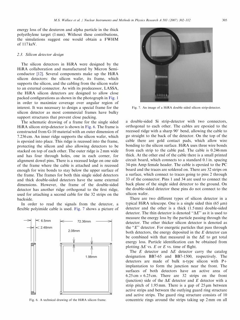
Fig. 7. An image of a HiRA double sided silicon strip-detector.
M.S. Wallace et al. / Nuclear Instruments and Methods in Physics Research A 583 (2007) 302–312 305
energy loss of the deuteron and alpha particle in the thickpolyethylene target (1mm). Without these contributions,the simulations suggest one would obtain a FWHMof 117 keV.
2.3. Silicon detector design
The silicon detectors in HiRA were designed by theHiRA collaboration and manufactured by Micron Semi-conductor [12]. Several components make up the HiRAsilicon detectors: the silicon wafer, its frame, whichsupports the silicon, and the cabling from the silicon waferto an external connector. As with its predecessor, LASSA,the HiRA silicon detectors are designed to allow closepacked configurations as shown in the photograph in Fig. 1in order to maximize coverage over angular region ofinterest. It was necessary to design a special frame for thesilicon detector as most commercial frames have bulkysupport structures that prevent close packing.
The schematic drawing of a frame for the single sidedHiRA silicon strip-detector is shown in Fig. 6. The frame isconstructed from G-10 material with an outer dimension of7.236 cm. An inner ridge supports the silicon wafer, whichis epoxied into place. This ridge is recessed into the frame,protecting the silicon and also allowing detectors to bestacked on top of each other. The outer ridge is 2mm wideand has four through holes, one in each corner, foralignment dowel pins. There is a recessed ledge on one sideof the frame where the cable is attached and is recessedenough for wire bonds to stay below the upper surface ofthe frame. The frames for both thin single sided detectorsand thick double-sided detectors have the same externaldimensions. However, the frame of the double-sideddetector has another ridge orthogonal to the first ridge,used for attaching a second cable for the 32 strips on thebackside.
In order to read the signals from the detector, aflexible polyimide cable is used. Fig. 7 shows a picture of
6.5mm
2.48mm2.08mm
72.36mm
1.98mm
Fig. 6. A technical drawing of the HiRA silicon frame.
a double-sided Si strip-detector with two connectors,orthogonal to each other. The cables are epoxied to therecessed ridge with a sharp 90� bend, allowing the cable togo straight to the back of the detector. On the top of thecable there are gold contact pads, which allow wirebonding to the silicon surface. HiRA uses three wire bondsfrom each strip to the cable pad. The cable is 0.246mmthick. At the other end of the cable there is a small printedcircuit board, which connects to a standard 0.1 in. spacing34-pin Amp female header. The cable is epoxied to the PCboard and the traces are soldered on. There are 32 strips ona surface, which connect to traces going to pins 2 through33 of the connector. Pins 1 and 34 are used to connect theback plane of the single sided detector to the ground. Onthe double-sided detector these pins do not connect to thesilicon wafer.There are two different types of silicon detector in a
typical HiRA telescope. One is a single sided thin ð65 mmÞdetector and the other is a thick (1.5mm) double-sideddetector. The thin detector is denoted ‘‘DE’’ as it is used tomeasure the energy loss by the particle passing through thedetector. The other thicker silicon detector is denoted asthe ‘‘E’’ detector. For energetic particles that pass throughboth detectors, the energy deposited in the E detector canbe combined with that measured in the DE to get totalenergy loss. Particle identification can be obtained fromplotting DE vs. E or E vs. time of flight.The E detector and DE detector carry the catalog
designation BB7-65 and BB7-1500, respectively. Thedetectors are made of bulk n-type silicon with Pþimplantation to form the junction near the front. Thesurfaces of both detectors have an active area of6:25 cm� 6:25 cm. There are 32 strips on the front(junction) side of the DE detector and E detector with astrip pitch of 1.95mm. There is a gap of 25mm betweenactive strips and between the outlying guard ring structureand active strips. The guard ring structure consists of 10concentric rings around the strips taking up 2mm on all
ARTICLE IN PRESS
Energy [MeV]5 10
Cou
nts
0
1000
2000
3000
4000
6 7 8 9
Fig. 8. A 228Th spectrum with a pulser peak above 10MeV for a single
strip of a HiRA double-sided silicon strip-detector.
Table 1
The energy resolution for the five strongest peaks in Fig. 7 given raw and
after subtracting electronics noise
a Energy (MeV) FWHM (keV) FWHMcorr (keV)
5.423 31.6 26.6
5.685 33.4 28.7
6.288 33.2 28.4
6.778 35.2 30.7
8.784 33.8 29.1
M.S. Wallace et al. / Nuclear Instruments and Methods in Physics Research A 583 (2007) 302–312306
sides. The 10 rings are all floating with respect to the frontor back voltages. This structure was added to reduce thesurface leakage current, particularly on the end strips. TheHiRA silicon detectors typically run with leakage currentsbelow 1 mA for DE detectors and 1–3mA for the E detectorsat room temperature.
On the back (ohmic) side of the DE detector is a singlealuminum electrode. The E detector (as shown in Fig. 7)has 32 strips on the back (ohmic) side. These strips areperpendicular to the strips on the front side. The pitch onthe back of the E detector is also 1.95mm but it has aninter-strip gap of 40mm as opposed to the 25mm on thefront. With strips on both sides an effective pixel, based onthe strips hit on the front and the back, can be created. Ifthe detector is mounted 35 cm from the target, which is thedesigned distance, the angular resolution is 0:15�. There isno guard ring structure on the back, which is at groundwhile voltage is applied to the front during typicalexperimental setups.
2.4. Specification and performance of the silicon detectors
All detectors were tested and resolution for each stripwas measured prior to use in an experiment. The detector isplaced inside a vacuum chamber with no foil between thedetector surface and an a source. A 1:2mCi 228Th sourcewith a thin 50 mg=cm2 gold window was used. The 228Thsource is a very nice calibration source as it contains eightdifferent energy alpha particles with substantial intensity.More than 100 keV separates five of these alphas. Thismakes them very easy to fit and extract the peak locationand FWHM. The highest alpha energy is 8.7MeV giving alarger signal than the 241Am source, which has the mostintense peak at 5.5MeV.
The source was placed approximately 20 cm from thedetector, illuminating all strips. Because the source–detector distance was less than the 35 cm, the collimationof the guard ring was not effective. Particles striking theguard ring generate signals with reduced energy on theedge. For this test, we used conventional electronics andthe detectors were connected to individual pre-amplifiersattached to the scattering chamber on the outside. (Thesepre-amplifiers were originally built for LASSA and arediscussed in Ref. [6].)
Fig. 8 is a spectra for an average EF strip, where EFrefers to the front strips of the E detector and EB refers tothe back strips. A Gaussian fit is performed for each peakexcluding the low energy tail, which is non-Gaussian foralpha particles. There is also a pulser peak around 14MeVwhich is used to measure the electronic component of theoverall resolution. Table 1 gives the FWHM resolution foreach of the alpha peaks as they were measured and theintrinsic ðFWHMcorrÞ values, where the electronic noisecontribution is subtracted in quadrature. The overallresolution is then taken to be the average resolution ofthe 5 strongest alpha peaks. For the strip shown in Fig. 8the intrinsic energy resolution is 28.6 keV FWHM.
2.5. Design and specifications of the CsI(Tl) detectors
Particles with higher energy, that will punch through the1.5mm Si detector, are detected in the CsI(Tl) scintillationcrystals. CsI(Tl) was chosen as the stopping material as ithas reasonable energy resolution, can be machined toappropriate dimensions, is far less hygroscopic than othercrystals such as NaI, and has a light output well suited forphotodiode readout. The CsI(Tl) detectors used in HiRAwere manufactured by Scionix. Fig. 9 shows a schematicside and front view of the CsI(Tl) crystals used in HiRA.The trapezoidal crystals are 3:5 cm� 3:5 cm on the frontand 3:9 cm� 3:9 cm in the rear with a thickness of 4 cm.Behind each crystal is a 3:9 cm� 3:9 cm� 1:3 cm lightguide which has been attached using BC 600 opticalcement. A 1:8 cm� 1:8 cm silicon photodiode was glued tothe photodiode with RTV615 silicon rubber glue. Eachcrystal is individually wrapped in cellulose nitrate mem-brane filter paper. The four crystals are then wrappedtogether with Teflon tape. The front surface of the crystalarray is covered with aluminized Mylar foil. The lightguides were painted with BC-620 reflective paint.All the HiRA CsI(Tl) crystals have light output
uniformity of 1% for 5.486MeV particles from an 241Amsource [13]. Details of the uniformity test are described inRef. [13]. In the same study, it was found that light outputnon-uniformities in the HiRA CsI(Tl) crystals due tosmooth variations in the thallium doping concentration
ARTICLE IN PRESS
CsI(Tl) Crystal
Light Guide Photo Diode
Fig. 9. A drawing of the HiRA CsI(Tl) crystals.
M.S. Wallace et al. / Nuclear Instruments and Methods in Physics Research A 583 (2007) 302–312 307
can be corrected. In addition to these smooth variations inlight output, local non-uniformities in light output at thelevel of 0.3% are present in our crystals. No process hasbeen identified so far that can eliminate or remove them.
3. Electronics for the array
The HiRA device consists of 1920 individual siliconstrips and 80 CsI(Tl) crystals whose signals must beamplified and digitized. The CsI(Tl) readout uses CAMACbased electronics that were developed earlier for theLASSA device [6]. The application of traditional electro-nics, where each strip has a discrete pre-amplifier, shaper,discriminator, TDC channel, and ADC channel, to thereadout of the HiRA silicon detectors would cost on theorder of one million dollars to implement. A lower costelectronics solution is required for HiRA and for otherlarge strip-detector arrays being developed for nuclear,particle, and space-based physics. The implementation ofthe HiRA Application Specific Integrated Circuit (ASIC),called the HINP16 within the HiRA readout electronics, isdescribed below. A more detailed description of ASICfunctionality is presented in a separate paper [14].
3.1. CsI(Tl) readout electronics
Each HiRA CsI crystal is associated with its own pre-amplifier board located within the telescope (see Fig. 2).Individual pre-amplifier circuits are removable for easyreplacement. Photodiodes attached to the CsI light guidesare connected directly to the pre-amplifier circuits. Thesecircuits are mounted to a small board within a singletelescope which provides routing to and from each pre-amplifier for power, signals and test signal inputs.Connection to this common board is via a 16-pin Ampconnector. Each telescope is then routed to a commoncircuit box located near the array; four telescopes areconnected to a single box so that 16 output signals
are routed to external CAMAC Pico System shaper/discriminator modules via a 34-pin ribbon cable [15].Output from the variable gain shaping amplifiers wasrouted to CAEN V785 VME ADCs; each 32 channelADC accommodates two Pico modules [16]. ADC gatingand readout triggering from events in the CsI is possiblevia a common discriminator OR signal from the discrimi-nator portion of the CAMAC modules or from adiscriminator multiplicity output. In the case of a readouttrigger other than that of the CsI (e.g., triggering via eventsin the silicon detectors), only the shaper modules arenecessary, as gating of the peak sensing ADCs can be viathis trigger.External electronics for the CsI readout of the entire
array consists of five 16-channel shaper/discriminatormodules and three 32-channel peak-sensing ADCs.
3.2. Application Specific Integrated Circuit (ASIC)
The HiRA detector is designed to be a versatile devicethat can be used in a variety of ways for different types ofexperiments. For some experiments the energy deposited inthe silicon detector is of the order of 50MeV with particlemultiplicities of 1 per event. Some require timing resolu-tions around 1 ns, others require energy depositions around500MeV with particle multiplicities greater than 20. Thismakes designing a single ASIC difficult; as the namesuggests they are application specific. The HiRA ASICcontains charge sensitive amplifiers, discriminators, shap-ing amplifiers, time to analog converters and a sample andhold circuit along with the digital logic necessary forcommunication and multiplexing the signals out. There are16 individual channels within each chip. Fig. 10 is a blockdiagram representation of the functionality of the HiRAASIC chip. The ASIC is fabricated in the AMIS 0:5mm,N-well CMOS, double-poly, triple-metal high-resistanceprocess through MOSIS [17].The first element of the ASIC, the charge sensitive
amplifier (CSA) consists of two different amplifiers as wellas the option to bypass it completely. User selectable CSAsallow for high and low gain settings to accommodatevarious detector applications. The low gain CSA gives alinear dynamic range of about 500MeV in silicon. The highgain setting allows particles up to about 100MeV in silicon.The CSA takes up a large physical area on the chip as alarge input MOSFET is required to achieve the requiredresolution. If a larger gain is required, then the chipbe connected to an external pre-amplifier by bypassing theon-board CSAs.After the CSA or external pre-amplifiers the signal is
split with one signal going into the Nowlin pseudoconstant-fraction discriminator (CFD) [18,19]. The dis-criminator consists of a zero-cross discriminator and aleading edge discriminator. It is the latter which sets thethreshold. The other signal is routed to a shaping amplifier,producing an approximately Gaussian shaped signal, witha shaping time of about 1ms. The signals can be positive or
ARTICLE IN PRESS
Hit Reg
Stop
TVCStart Peak Find
Peak Hold
Peak Hold
Peak Find
HiRA ASIC block diagram for one channel
Inspection Points
Hi
Lo
OR
Pseudo CFD
Shaper
External Stop
HP-Filter
CSA
Fig. 10. A diagram of one channel of the HiRA ASIC.
Fig. 11. Image of a HiRA chipboard and a prototype chip with a quarter
for reference.
M.S. Wallace et al. / Nuclear Instruments and Methods in Physics Research A 583 (2007) 302–312308
negative. The shaper is a unity gain amplifier so all the chipgain comes from the CSA.
The discriminator has a trigger threshold controlled byan internal digital-to-analog converter (DAC), which canbe set both positive and negative for either input level foreach of the 16 channels individually. The discriminatoroutput has three functions, start a time-to-voltageconverter (TVC), update a hit register, which can be usedto determine trigger criteria, and initiate a peak search.When a discriminator fires, the shaped signal will gothrough a peak find circuit and the peak value willbe held until it is read out or forced to clear. The TVC,which has two time range settings of about 150 ns and1ms, is stopped by an external common stop signal. Thepeak of the time signal is then stored until it is read orforced clear.
Each ASIC has a computer controlled external output ofthe signal after the CSA, after the shaper, and thediscriminator logic signal as denoted by solid black circleson Fig. 10. For details on the ASIC see Ref. [14].
3.3. Implementation of the HINP16 within the HiRA
readout electronics
The HiRA silicon detectors have 32 strips per surface; sotwo ASICs are needed per surface. The ASICs are mountedon chipboards in pairs along with other components.Fig. 11 shows one of the chipboards with two ASIC chipson it. Below the chipboard is a 4 channel prototype chipwith the cover off exposing the actual ASIC. A US quartercoin is placed next to it for size comparison. Additionallyon the chipboard are bias resistors and decouplingcapacitors for the bias voltage going to the detectors aswell as a complex programmable logic device (CPLD)to mediate internal and external chip logic. There isalso a differential-amplifier for the energy and time signals.These signals are multiplexed out of the chips and intothe differential amplifier generating a differential signalbetween �1 and þ1V.
One chipboard is required for each surface of silicon;therefore three are used for each telescope. An additionalcircuit board called the motherboard is used to simulta-neously provide power and serial logic signals to several
chipboards and multiplexing functions for sampled signals.The first experiments with HiRA utilize detectors aligned intowers of up to 5 detectors. A motherboard was built thatcan accept 16 chipboards, which are needed for a tower ofup to 5 telescopes.The motherboard contains a field programmable gate
array (FPGA), and level translators between the externalcontrol logic and the FPGA and the other circuits on thechipboards. The FPGA is used to communicate with up to32 chips on the 16 chipboards that the motherboard canservice. For each motherboard there are two linearoutputs. One contains the sequence of energy values forall channels that have a valid hit register event. The othercarries the corresponding time values from the TACs. Inaddition to this, there is logic information coming out on ahigh-density logic control cable to communicate theaddress of each energy and time value sent out from themotherboard.
ARTICLE IN PRESS
Fig. 12. An image of the side of a HiRA telescope showing the insertion
slot for alpha calibrations.
M.S. Wallace et al. / Nuclear Instruments and Methods in Physics Research A 583 (2007) 302–312 309
Each motherboard has three separate computer con-trolled logic OR signals such that any number of thechipboard OR signals can be set in any combination. Thereare also three Sum signals, which are also set via computercontrol. The Sum signal represents an analog level basedon the multiplicity. There are six linear inputs for pulsers.They are divided into three for even channels and three forodd channels. Jumpers on the motherboard steer thesepulser inputs to specific chipboards slots.
Aside from the motherboard, one only needs two VMEmodules to handle all information with the electronics.The first is a SIS3301 105MHz sequencing ADC thatcontains 4 pairs of sampling ADCs [20]. Each motherboarduses one pair from the sampling ADC. The connectionfrom the motherboard to the ADC is via a dual lemocable. There is an external clock input that tells the ADCwhen to sample each of the four pairs. The control of thereadout and the storing of addresses from each mother-board along with the ADC clock are handled by anXLM80 universal logic module made by JTEC [21]. TheXLM80 contains an additional FPGA, which is pro-grammed with the trigger logic sequences for the silicondetectors.
The ASICs were designed to run in sparse readout, inwhich a discriminator signal sets a hit register for aspecific channel. The hit register bit is then required forreadout of that channel to occur. This is highly desirableas otherwise the readout time for an entire towercan be quite long. There are situations where one mightwant to force-read electronic channels that did not triggertheir discriminators. For this reason software was devel-oped to force the discriminators on all channels to trigger,initiating a full read of all detectors connected to thismotherboard.
4. Calibration and particle identification
The HiRA device provides the possibility to performprecise measurements of direct reactions, two- and multi-particle correlations and resonance spectroscopy usingboth stable and rare isotope beams. The accuracy of suchmeasurements, however, depends significantly on theaccuracy with which HiRA can be calibrated in mass,charge, energy and angle. Here we describe how the devicewas designed to allow accurate measurements of theenergy, charges and masses of the various species. Inanother article, we describe a Laser Based AlignmentSystem (LBAS) that was developed to determine thelocation of each strip relative to the target [22].
When two layers of silicon are used, the design allows theinsertion of a pin source to calibrate the 1.5mm detectorwithout having to first remove the 65 mm detector. Since thelight output of the CsI(Tl) scintillator is particle dependent,the calibration of the CsI(Tl) detector requires beamparticles and a precision pulser. Mass and chargeidentification can be easily obtained from the correlationbetween the energy loss and the total energy of the particle.
4.1. Calibration of Si detectors with external source
In general, the first layer of silicon can easily becalibrated by placing an alpha source at the target location.The same procedure used to determine the energyresolution of the detector is adopted. The alpha decaypeaks shown in Fig. 14 are used to calibrate each strip ofthe detectors. To monitor any gain shift during theexperiment, we took data with alpha source when beamswere not available.
4.2. Pin source calibration
For experiments with telescopes each of which containstwo silicon detectors, the second one is completely behindthe first. This makes access to the second detector difficultin order to calibrate using alpha sources. To minimize thehandling of silicon detectors, mounting and dismountingthem, during alpha source calibrations, a slot is designedon one side of the silicon box as shown in Fig. 12 to fit acalibration source between the silicon detectors. It allows athin frame, with an alpha source on a pin, to slide betweenthe silicon detectors.Figure 13 is a picture of one of these source frames. The
pin is a 0.5 in. long dowel pin. This pin is activated byelectroplating the tip with daughter nuclei from a 228Thsource. The source can be generated in 24 h or less. Theunactivated side of the pin is then glued onto the frame asshown in Fig. 13. There are three strong alpha lines fromthis source at 8.785, 6.050, and 6.089MeV. The primarydeposition on the pin is 212Pb isotope which have a half-lifeof 10.6 h. As there is no additional material between theradioactive nuclei and the surface this source can producevery sharp energy spectra as shown in Fig. 14.The pin source is capable of hitting all pixels on the E
detector as shown in Fig. 15. Due to the close proximity tothe silicon surface, about 3mm, the alpha particle strikesthe surface with large oblique angles for pixels that are notnear the center. The dead layer on the surface of the siliconwill shift the energy of the alpha particles and diminish theenergy resolution. If there is enough data from reactionswith the beam, one can calibrate using only the pixel or
ARTICLE IN PRESS
Fig. 13. An image of the alpha calibration source frame and source pin.
Energy [Channels]
0 200 400 600 800 1000 1200 1400
Co
un
ts
0
20
40
60
80
100
120
140
160
180
Fig. 14. An energy spectrum from the pin source gated on the 16th strip
on EF and the 16th strip on EB.
EB Strip Number
0 5 10 15 20 25 30
EF
Str
ip N
um
ber
0
5
10
15
20
25
30
10
102
103
Fig. 15. The two-dimensional hit pattern from a pin source inserted
between the two silicon detectors of a HiRA telescope.
M.S. Wallace et al. / Nuclear Instruments and Methods in Physics Research A 583 (2007) 302–312310
pixels directly in front of the pin source, thus avoidingproblems with angle and dead layer measurements.
Given the nature of double-sided silicon detectors it ispossible to calibrate the energy for all strips if one canaccurately calibrate a single strip on the front surface andthe back surface. For example, using the pin source, Strip16 on the front and back are calibrated. Fig. 14 is a
histogram of strip 16 on the front surface of an E detectortaken with a pin source inserted between the DE detectorand E detector. This histogram is gated on events with onlyone coincidence hit on both front and back strips.Requiring a signal in strip 16 on the back, effectivelyselecting alpha particles that hit the central pixel, 16–16.This pixel should have zero incident angles giving the mostaccurate energy measurement. The two high intensity alphapeaks are fitted, and a linear calibration is done for thesetwo strips. New parameters are then generated with strips16 on EF and EB calibrated in MeV.For every particle incident on the silicon, the energy is
measured in one strip on the front, and one strip on theback regardless of where the particle hits the surfaceof the detector. The energy measured by each of thesestrips should be exactly the same. Thus all particlesincident on EF16 can be used to calibrate the correspond-ing EB strips.
4.3. CsI(Tl) calibration
Since the light output of CsI(Tl) crystals are particledependent and non-linear, the calculation has to beperformed for each isotope of interest. In one of the HiRAexperiments, a mixed beam of p, d, t at 86.1, 44.53 and29.93MeV at Br ¼ 1:3716Tm, was produced from theNSCL coupled-cyclotron-A1900 [23–25]. The beams scat-tered off elastically from a Au target of 20mg=cm2 effectiveareal thickness. To increase statistics in the extraction ofthe elastically scattered peak, all the strips in the E
detectors are calibrated and a particle identification spectrasimilar to Fig. 16 are generated. Fig. 17 shows the peaks ofthe three hydrogen isotopes, p, d, and t. The peaks arerather sharp and form a nearly linear function between theADC channel and the particle energy. For experimentswhere more than the hydrogen isotopes are detected,
ARTICLE IN PRESS
Energy [Channels]
100 200 300 400 500
Counts
0
2000
4000
6000
8000
10000
Tritons
Deuterons
Protons
Fig. 17. Calibration spectrum for CsI(Tl) using elastic scattering of light
charged particles.
CsI Energy [Channels]
500 1000 1500 2000 2500 3000
EF
Energ
y [M
eV
]
5
10
15
20
25
0
5
10
15
20
25
30
35
40
Fig. 16. A PID spectrum using the CsI and thick silicon.
EF Energy [MeV]
0 5 10 15 20 25 30
DE
Energ
y [M
eV
]
0
2
4
6
8
10
12
14
0
1
2
3
4
5
6
7
8
Fig. 18. A PID spectrum using both silicon detectors.
M.S. Wallace et al. / Nuclear Instruments and Methods in Physics Research A 583 (2007) 302–312 311
calibrations with many cocktailed beams and preferablywith isotopes of different energy range will be needed.
4.4. Particle identification
Of critical importance in a detection array such as HiRAis the ability to identify the masses and charges of variousparticles, as well as energy of various particles to anexcellent degree of resolution. For particle identification,HiRA relies on the technique of energy loss, DE vs E
identification. There are two types of DE vs E plots that areused to identify particles detected with HiRA depending onthe particle energy. For high-energy particles that penetrateinto the CsI detectors the second Si detector is used as a DE
detector, with the particle stopping in the CsI, which islabeled as the E detector. Fig. 16 is a DE–E plot forparticles produced by the fragmentation of a 40Ca beamimpinging on a plastic target. One can see lines corres-ponding to p, d, t hydrogen isotopes as well as linescorresponding to 3He and 4He.
If the energy of particles is lower, then the particles stopin the second silicon detector. In this case the DE detectormeasures DE and the second Si detector gives the residualenergy. Fig. 18 represents the corresponding DE–E plotobtained in the beam described above.Clearly HiRA can identify both the charge number ðZÞ,
and the mass number ðAÞ for light charged particles. Up tothis point, no data has been measured for heavierfragments. However, based on our experience with theLASSA array, HiRA is expected to have particle identifi-cation up to oxygen isotopes.
5. Summary
A new charged particle array has been built andcharacterized. To date the array has been used to performfive different experiments. In these experiments thedetectors were arranged in four different physical config-urations, showing the devices versatility and usefulness forstudies of rare isotope research.
References
[1] MSUCL-939, The K500�K1200, A coupled cyclotron facility
at the National Superconducting Cyclotron Laboratory, The
K500�K1200, A Coupled Cyclotron Facility at the National
Superconducting Cyclotron Laboratory (July 1994).
[2] T. Kubo, M. Ishihara, N. Inabe, H. Kumagai, I. Tanihata,
K. Yoshida, Nucl. Instr. and Meth. B 70 (1992) 309.
[3] W. Mittig, J. Phys. G 24 (1998) 1331.
[4] H. Geissel, et al., Nucl. Instr. and Meth. B 70 (1992) 286.
[5] W.N. Catford, C.N. Timis, M. Labiche, R.C. Lemmon, G. Moore,
R. Chapman, The TIARA array for the study of nucleon transfer
reactions, in: Applications of Accelerators in Research and Industry:
17th International Conference, American Institute of Physics, 2003,
pp. 329–332.
[6] B. Davin, et al., Nucl. Instr. and Meth. A 473 (2001) 302.
[7] Y. Blumenfeld, et al., Nucl. Instr. and Meth. in Phys. Res. A 421
(1999) 471.
[8] E. Pollacco, et al., MUST II: Large solid angle light charged particle
telescope for inverse kinematics studies with radioactive beams, in:
ARTICLE IN PRESSM.S. Wallace et al. / Nuclear Instruments and Methods in Physics Research A 583 (2007) 302–312312
J.L. Duggan, I.L. Morgan (Eds.), AIP Conference Proceedings, vol. 680:
Application of Accelerators in Research and Industry, 2003, pp. 313–316.
[9] D. Bazin, J.A. Caggiano, B.M. Sherrill, J. Yurkon, A. Zeller, Nucl.
Instr. and Meth. B 204 (2002) 629.
[10] D. Shapira, T.A. Lewis, L.D. Hulett, Nucl. Instr. and Meth. A 454
(2000) 409.
[11] D. Bazin, O. Tarasov, M. Lewitowicz, O.S. Lise, Nucl. Instr. and
Meth. A 482 (2002) 307–327. URLhhttp://www.nscl.msu.edu/lisei.
[12] Micron Superconductor LTD, 1 Royal Buildings, Marlborough
Road, Lancing, Sussex BN158UN, England.
[13] M.-J. van Goethem, M.S. Wallace, B.E. Nett, M.A. Famiano,
K.R. Herner, D.J. Oostdyk, M. Mocko, W.G. Lynch, M.B. Tsang,
P. Schotanus, J. Telfer, H.L. Clark, A. Moroni, R.D. de Souza,
L.G. Sobotka, Nucl. Instr. and Meth. A 526 (2004) 455.
[14] G.L. Engel, M. Sadasivam, M. Nethi, J.M. Elson, L.G. Sobotka,
R.J. Charity, Nucl. Instr. and Meth. A 573 (2007) 418.
[15] Pico Systems, 534 Lindeman Rd. Kirkwood, MO 63122.
[16] CAEN Technologies, Inc 1140 Bay Street, Suite 2C, Staten Island,
NY 10305.
[17] MOSIS, 4676 Admiralty Way, 7th Floor Marina del Rey CA 90292-
6695.
[18] C.H. Nowlin US Patent no. 4,443,768, April 17, 1984.
[19] C.H. Nowlin, Rev. Sci. Instr. 4 (1992) 2322.
[20] SIS GmbH Harksheider Str. 100A 22399 Hamburg, Germany.
[21] JTEC Instruments, 32 Thompson Rd. Rochester, NY 14623.
[22] A. Rogers, et al., Nucl. Instr. and Meth. A manuscript in preparation.
[23] I. Wiedenhover, M. Steiner, D.J. Morrissey, B.M. Sherrill, D. Bazin,
J. Stetson, A. Stolz, O. Tarasov, J. Yurkon, the NSCL staff, AIP
Conf. Proc. 610 (2002) 937.
[24] D.J. Morrissey, B.M. Sherrill, M. Steiner, A. Stolz, I. Wiedenhoever,
Nucl. Instr. and Meth. B 204 (2003) 90.
[25] A. Stolz, T. Baumann, T.N. Ginter, D.J. Morrissey, M. Portillo,
B.M. Sherrill, M. Steiner, J.W. Stetson, Nucl. Instr. and Meth. B 241