Faculty of Electrical Engineering, Mathematics & Computer Science ASIP Design on behalf of hybrid beamforming in MIMO communication system Ashwini Pohekar Thesis Report October 2019 Supervisors: dr. ir. S. H. Gerez dr. ir. A. B. J. Kokkeler dr. ir. M. S. Oude Alink Masoud Abbasi Alaei (M.Sc.) Computer Architecture and Embedded Systems Group Faculty of Electrical Engineering, Mathematics and Computer Science University of Twente P.O. Box 217 7500 AE Enschede The Netherlands
Transcript
1
Faculty of Electrical Engineering,Mathematics & Computer Science
ASIP Designon behalf of hybrid beamforming in
MIMO communication system
Ashwini PohekarThesis ReportOctober 2019
Supervisors:dr. ir. S. H. Gerez
dr. ir. A. B. J. Kokkelerdr. ir. M. S. Oude Alink
Masoud Abbasi Alaei (M.Sc.)
Computer Architecture and Embedded Systems GroupFaculty of Electrical Engineering,
Mathematics and Computer ScienceUniversity of Twente
P.O. Box 2177500 AE Enschede
The Netherlands
ii
Abstract
In this thesis, an Application Specific Instruction Set Processor (ASIP) is developed to cal-culate optimum analog beamforming coefficients for a hybrid beamformer in a Multiple InputMultiple Output (MIMO) communication system. MIMO technology offers promising solu-tions to meet the increasing data-rate requirements. A lot of research is being carried outto improve the feasibility of these systems. Hybrid beamforming systems aim at reducingthe problems faced by MIMO. Hybrid beamforming essentially involves beamforming in theanalog as well as the digital domain. The ASIP proposed in this assignment is aimed atcalculating optimum coefficient values for the analog beamformer. This thesis presents thedifferent design decisions taken while developing the ASIP, the detailed design flow under-taken in the processor modeling tool and the implementation of the target application on areference design. Additionally, comparison results against a floating point processor havealso discussed to show the performance (and energy) efficiency of the designed ASIP.
iii
IV
Preface
This research is the product of collective efforts put in by many people and I take this oppor-tunity to acknowledge their contributions. First and foremost, I would like to thank my dailysupervisor Masoud Abbasi Alaei and my main supervisors dr. ir. Sabih Gerez who havebeen of immense help to me and without their guidance, this project would not have beenpossible. I express my gratitude for their interesting solutions for the problems I faced duringwork and all the encouragement that pushed me forward to deliver my best. I am also highlygrateful to them for providing me with all the possible facilities required for the successfulcompletion of the project.
I would also like to thank my committee members dr. ir. A. B. J. Kokkeler and dr. ir. M. S.Oude Alink for their valuable advice. Furthermore, I would like to thank A.C.R. WijesundaraRanasinghe Appuhamilage for assisting me in the synthesis process and working with UMC65 nm technology.
I would also like to extend my gratitude to L. J. Helthuis for all the assistance he providedin the tool installation process and while dealing with any technical issue.
At last, I would like to express my hearty gratitude to my parents and my friends for theirunwavering faith in me and undying support that kept me strong emotionally through theentire journey of my graduate program.
Over the past several decades, use of Multiple Input Multiple Output (MIMO) technology incommunication systems has increased substantially. Wi-Fi networks, cellular 3G / 4G LTE& 5G massive MIMO systems are a few prominent examples where MIMO technology isbeing used in modern communication infrastructure. MIMO is a promising technology tomeet the growing demands of high data rate wireless communication. More recently, MIMOhas been finding its way into rapidly growing markets such as professional broadcast video,law enforcement, and government sectors. Although, MIMO technology has already beenput to use, a lot of research is being carried out in this field and still many questions areraised over its viability.
The introduction of multiple antennas at the transmitter and receiver increases the over-all complexity of the system. This increased complexity is seen in terms of increased circuitsize, power consumption and higher computation capacity requirement [1]. A promising so-lution to these problems lies in the concept of hybrid beamforming in MIMO communicationsystems. Hybrid beamforming involves the usage of analog beamforming in the RF domainand digital beamforming in the baseband domain. This concept was introduced by one ofthe authors in [2] and [3], in the mid-2000s. Hybrid beamforming was originally formulatedkeeping in mind MIMO communication systems which have arbitrary number of antennasbut it was later also applied to massive MIMO systems. The interest in hybrid MIMO sys-tems has accelerated over the past three years and various transceiver structures have beenproposed in literature.
With this brief glimpse into the history of MIMO communication systems and short intro-duction to hybrid beamforming, in the next subsection, MIMO communication systems andtheir operational complexity are summarized.
1.1 MIMO communication systems
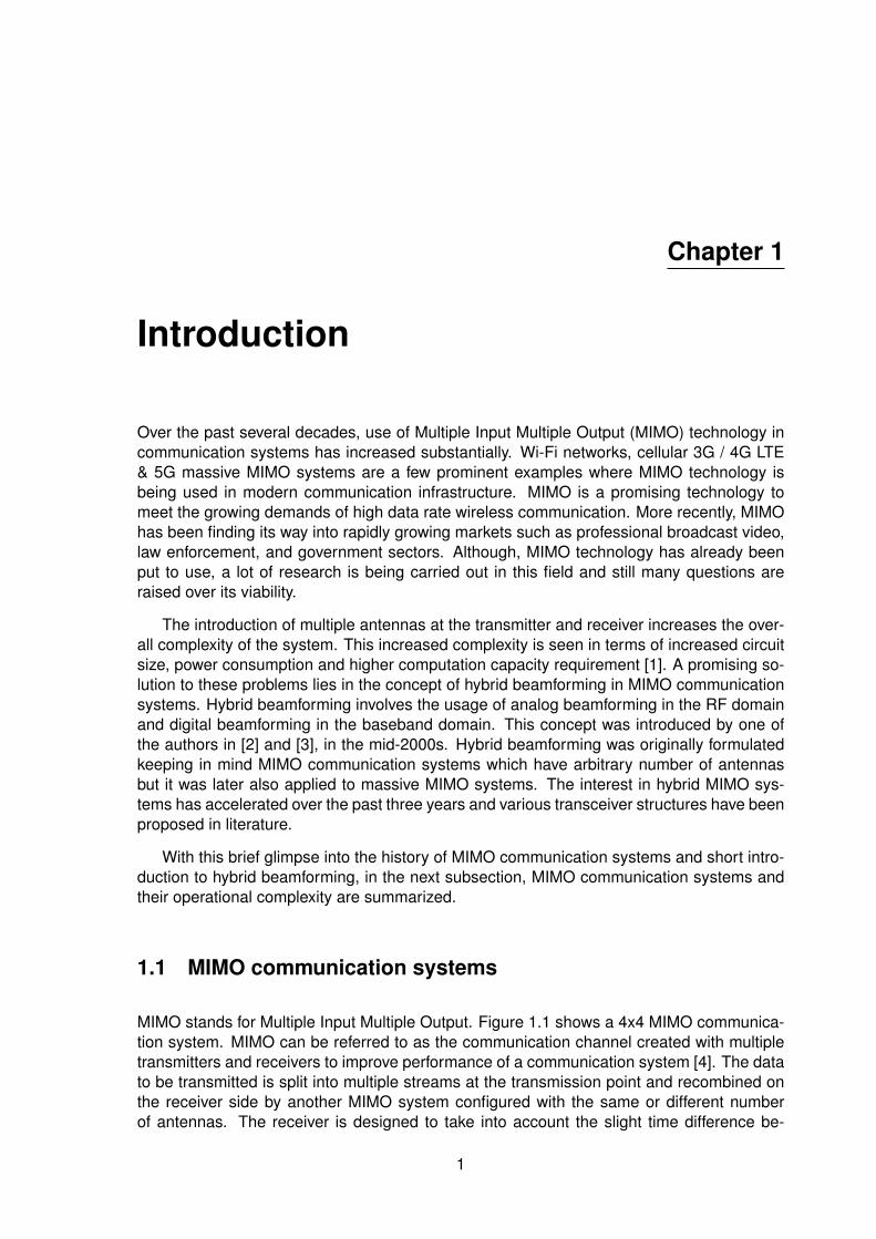
MIMO stands for Multiple Input Multiple Output. Figure 1.1 shows a 4x4 MIMO communica-tion system. MIMO can be referred to as the communication channel created with multipletransmitters and receivers to improve performance of a communication system [4]. The datato be transmitted is split into multiple streams at the transmission point and recombined onthe receiver side by another MIMO system configured with the same or different numberof antennas. The receiver is designed to take into account the slight time difference be-
1
2 CHAPTER 1. INTRODUCTION
tween reception of each signal, any additional noise or interference, and even lost signals.MIMO is able to ascertain different paths over the air interface by using multiple antennasat both ends, thus creating sub-channels within one radio channel and increasing the datatransmission (or capacity) of a radio link (or channel).
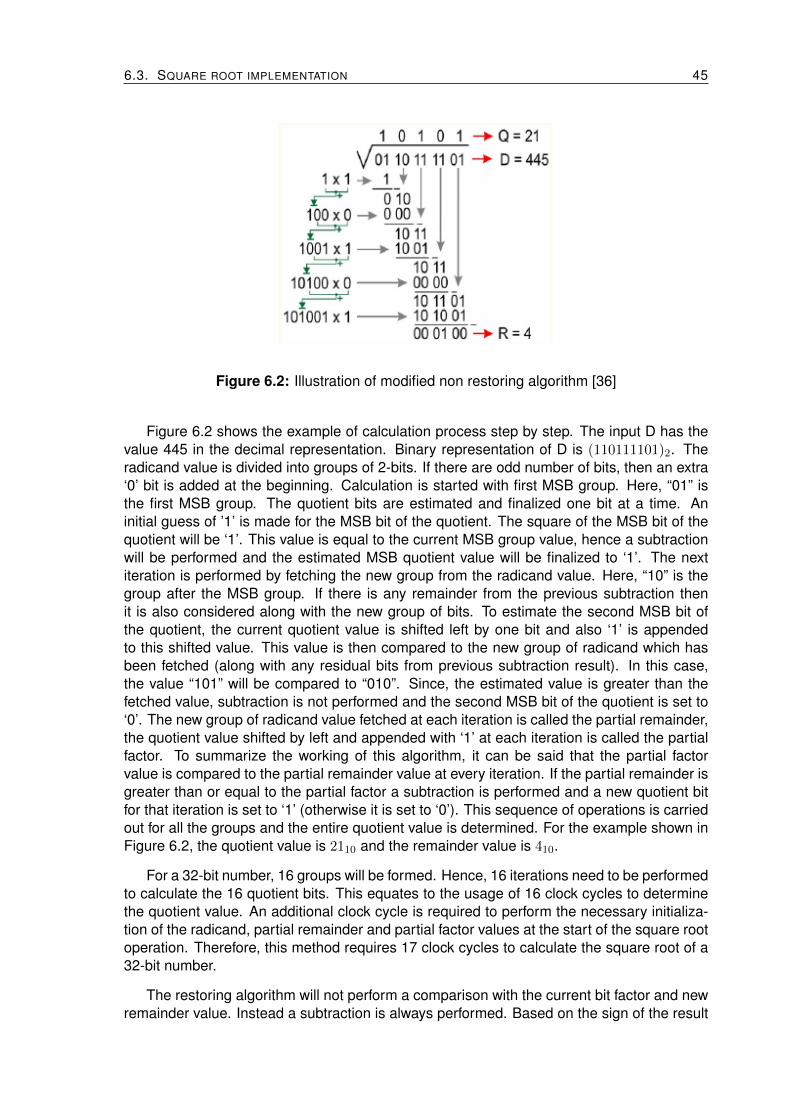
Figure 1.1: A 4x4 MIMO communication system [5]
Although, multiple transmitters and receivers help in overcoming the shortcomings ofsignal reflection and providing high data-rates, the design of such systems is a demandingtask. In order to facilitate the transmission of multiple data streams, signal processing isinvolved both at the transmitter and the receiver. Precoding (done at the transmitter) andequalization (done at the receiver) are some of the signal processing operations involved inMIMO systems. All these operations are computationally complex and come at a reasonablecomputational cost (processing power).
In the presence of multiple data streams beamforming needs to be performed for direc-tional transmission or reception of data. Traditionally in MIMO systems, this beamforming isperformed in the baseband domain. This beamforming is generally performed by a digitalsignal processor. When beamforming is performed only in the digital domain, the area of thehardware required is large. The power consumed for beamforming is also quite high in suchsituations, especially for the Analog to Digital Converter (ADC)s. In case of a hybrid receiversystem, the analog as well digital domain contribute towards the beamforming operation.This reduces the number of ADCs required and as result the area and power consumptionalso reduces.
Beamforming operation requires calculation of the optimal weights which help in recov-ering the original transmitted data streams. In case of a hybrid receiver, the process ofcalculation of these optimal weights needs to be performed for both the analog beamformerand digital beamformer. In this research assignment, the Application Specific Instruction SetProcessor (ASIP) is used to perform the calculation of optimum weights for the analog beam-former. The next section introduces the concept of ASIPs and also explains the motivationof choosing ASIP design in this assignment.
1.2 ASIP
ASIP stands for Application Specific Instruction-set Processor and it refers to a special classof processors which are designed for an application domain. As a rule of thumb, general-purpose processors are designed keeping in mind that the maximum performance and flex-
1.3. PROBLEM STATEMENT 3
ibility is achieved. The instruction set of these processors is such that, it is generic enoughto support different types of common applications. Additionally, the compiler is such that itis capable of offering compilation for all programs and adapting to all programmers‘ codingbehaviors. However, in case of ASIPs the instruction set is specifically developed such thatexecution of complex and frequently used functions in a given application is accelerated. Soin contrast to general-purpose processors, the flexibility of an ASIP is kept sufficient enoughinstead of very high, while the performance is kept very high specific to the application.
An ASIP hardware architecture typically will contain a number of suitably designed ap-plication specific functional blocks and the necessary interconnects to move around datato/from memory blocks under the control of the top level controller (control circuit) of theprocessor. Due to their application oriented nature, ASIPs [6] allow alteration of hardware-software boundary to meet the speed and energy constraints of the target application whileaffording programmability and flexibility in functionality.
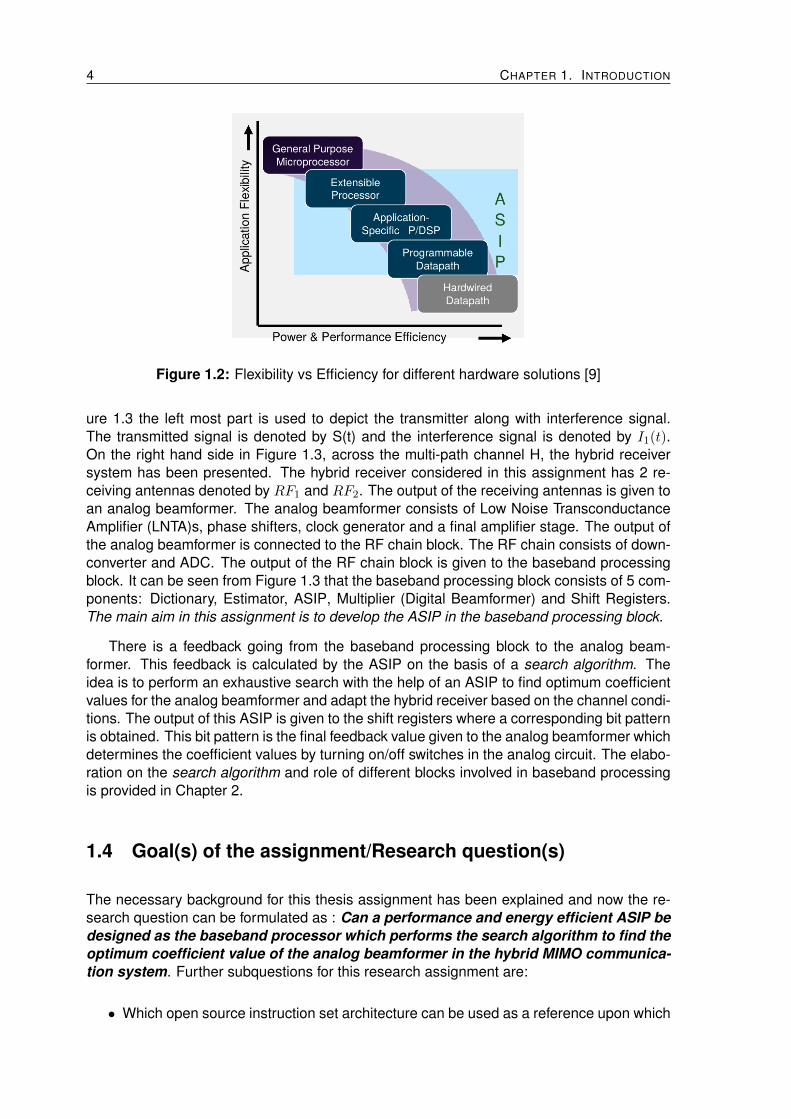
Figure 1.2 shows the comparison between flexibility and efficiency for different hardwareconfigurations. On one end there are general-purpose processors which provide very highapplication flexibility but are relatively low in terms of power and performance efficiency.On the other end, there are hardwired datapaths which in principal offer almost no flexibil-ity but offer very high power and performance efficiency. In between these two extremesare the ASIPs. ASIPs provide with hardware solutions which deploy classic techniques ofparallelism and custom datapaths; while maintaining flexibility through software program-ming. Some examples of ASIPs are application specific DSP processors, accelerators, co-processors etc. Parallel processing Ultra Low Power platform (PULP) [7] and OpenPiton [8]are examples of open source platforms which deploy ASIPs (based on RISC-V, OpenSPARCinstruction set resp.) designed for embedded vision, DSP computations, customizable par-allel processing, etc.
The optimum weight calculation for analog beamforming to be implemented in the ASIPrequires a lot operations based on the complex numbers and matrices. Hence, the design ofan ASIP which has custom datapath for handling these complex operations is chosen. Whileproviding the option of a custom datapath, the design of the ASIP will be flexible enough tohandle changes in the search algorithm, if any, in the future. The ASIP is a solution whichtries to provides the best of both worlds : flexibility and efficiency (power and performance). Itis always possible that one or more hardware solutions are better out of the different optionspresented in the design space shown in Figure 1.2 . Hence, the choice of ASIP design mustalso be seen as a design constraint in this thesis assignment.
1.3 Problem statement
Having briefly discussed MIMO communication systems and ASIPs, the motivation behindthis thesis assignment can be discussed. The introduction of multiple antennas at the trans-mitter and receiver side requires beamforming to be performed to recover the transmitteddata streams. The main focus in this thesis assignment is on hybrid beamforming as pre-sented in the following research papers [1], [10] and [11]. The in-depth information on work-ing of MIMO communications systems, its drawbacks and beamforming has been providedin Chapter 2.
The proposed hybrid system in this research assignment is shown in Figure 1.3. In Fig-
4 CHAPTER 1. INTRODUCTION
Figure 1.2: Flexibility vs Efficiency for different hardware solutions [9]
ure 1.3 the left most part is used to depict the transmitter along with interference signal.The transmitted signal is denoted by S(t) and the interference signal is denoted by I1(t).On the right hand side in Figure 1.3, across the multi-path channel H, the hybrid receiversystem has been presented. The hybrid receiver considered in this assignment has 2 re-ceiving antennas denoted by RF1 and RF2. The output of the receiving antennas is given toan analog beamformer. The analog beamformer consists of Low Noise TransconductanceAmplifier (LNTA)s, phase shifters, clock generator and a final amplifier stage. The output ofthe analog beamformer is connected to the RF chain block. The RF chain consists of down-converter and ADC. The output of the RF chain block is given to the baseband processingblock. It can be seen from Figure 1.3 that the baseband processing block consists of 5 com-ponents: Dictionary, Estimator, ASIP, Multiplier (Digital Beamformer) and Shift Registers.The main aim in this assignment is to develop the ASIP in the baseband processing block.
There is a feedback going from the baseband processing block to the analog beam-former. This feedback is calculated by the ASIP on the basis of a search algorithm. Theidea is to perform an exhaustive search with the help of an ASIP to find optimum coefficientvalues for the analog beamformer and adapt the hybrid receiver based on the channel condi-tions. The output of this ASIP is given to the shift registers where a corresponding bit patternis obtained. This bit pattern is the final feedback value given to the analog beamformer whichdetermines the coefficient values by turning on/off switches in the analog circuit. The elabo-ration on the search algorithm and role of different blocks involved in baseband processingis provided in Chapter 2.
1.4 Goal(s) of the assignment/Research question(s)
The necessary background for this thesis assignment has been explained and now the re-search question can be formulated as : Can a performance and energy efficient ASIP bedesigned as the baseband processor which performs the search algorithm to find theoptimum coefficient value of the analog beamformer in the hybrid MIMO communica-tion system. Further subquestions for this research assignment are:
• Which open source instruction set architecture can be used as a reference upon which
1.5. REPORT ORGANIZATION 5
+++
Figure 1.3: Hybrid beamforming structure at the receiver
the ASIP can be developed?
• Given the insights obtained by profiling of the algorithm on the chosen open sourcearchitecture, how can its performance be improved by an ASIP architecture optimizedfor the task?
• What design choices should be made while developing the architecture of the ASIP?For instance, How are complex numbers handled?, What must be the depth of thepipeline?, etc.
1.5 Report organization
The remainder of this report is organized as follows:
Chapter 2 discusses the concepts of MIMO communication, beamforming, formulationof the search algorithm, related work and the role of ASIP and other components inthe baseband domain.
In Chapter 3, the choice of a reference open source instruction set architecture isdiscussed.
In Chapter 4, the work flow of processor modeling tool used in this research assign-ment is shortly described along with detailed explanation of how each step of proces-sor design works.
Chapter 5 gives the necessary information about the Tzscale processor. The Tzscaleprocessor is the reference open source design (based on RISC-V ISA) upon which thetarget ASIP is to be developed.
Chapter 6 explains the design methodology followed for the ASIP implementation.
The report then concludes with Chapter 7 on Results and Evaluation, and Chapter 8on Conclusion and Future Work.
6 CHAPTER 1. INTRODUCTION
Chapter 2
Hybrid Beamforming in MIMOcommunication system
This chapter provides a detailed explnation of hybrid beamforming in MIMO communicationsystems. Initially, Single Input Single Output (SISO) systems along with the concepts ofdiversity and beamforming are presented. This is followed by a brief explanation aboutthe working of MIMO systems and hybrid beamforming, and the formulation of the searchalgorithm. Subsequently, literature research is presented to show the different ASIPs whichare currently being used in MIMO systems. The chapter finally concludes with a summaryof the components involved in the baseband processing domain of the hybrid beamformer.
2.1 SISO to MIMO
SISO stands for Single Input Single Output and it is the conventional system technologyused in communication. Generally, the signal transmitted from a single antenna is termedas the ‘input’, whereas signal received on a single antenna is termed as the ‘output’. Cellularphones have a single antenna which communicates with a single antenna at the base sta-tion. There are multiple users present in a communication system at any given point in timeand they require access to the cellular services simultaneously. In order to fulfill the require-ments of each user, the signals to the users are separated in time (Time Division MultipleAccess (TDMA)), in frequency (Frequency Division Multiple Access (FDMA)), or code (CodeDivision Multiple Access (CDMA)).
The features of the radio environment influence the quality of the communication linkbetween the transmit and receive antenna. The signal strength will vary as the user movesover both a small and large scale. In some cases this variation can cause the quality of thelink to become too low to deliver data successfully. This can cause radio link failure dueto unacceptable error rates. This problem can be combated by using a technique calleddiversity. Diversity [12] relies on the use of multiple copies of the same signal, which thereceiver can combine or select from. The idea behind it is that, even if one copy of the signalis of poor quality, it is unlikely that all the copies will be so, and therefore this redundancyallows the communication quality to be maintained.
The different types of diversity domains can be distinguished on the basis of how themultiple copies of the transmitted signal are generated. For instance, when multiple copies
7
8 CHAPTER 2. HYBRID BEAMFORMING IN MIMO COMMUNICATION SYSTEM
of the same signal are transmitting multiple times, it gives rise to time diversity; when multiplecopies of the same signal are transmitted at different parts of the spectrum, it gives rise tofrequency diversity. Diversity can also be achieved using the space domain. When thesame signal is transmitted from several base station antennas and received at a singlemobile terminal (large-scale or site diversity), or a receiver has several spatially separatedantennas each of which receives a different copy of the signal (small-scale diversity).
Transmit and receiver diversity techniques can be distinguished on the basis of which endof the communication link is under consideration. In transmit diversity techniques multiplecopies of the same signal are transmitted from several antennas and their superpositionis received at a single antenna. This diversity technique leads to the Multiple Input SingleOutput (MISO) system. In receive diversity techniques multiple copies of the same signalsent by a single transmit antenna are received at several antennas at the receiver. Thisdiversity technique leads to the SIMO system.
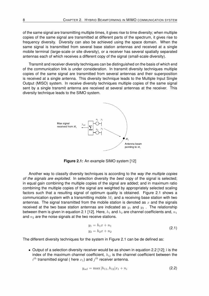
Figure 2.1: An example SIMO system [12]
Another way to classify diversity techniques is according to the way the multiple copiesof the signals are exploited. In selection diversity the best copy of the signal is selected;in equal gain combining the multiple copies of the signal are added; and in maximum ratiocombining the multiple copies of the signal are weighted by appropriately selected scalingfactors such that a resulting signal of optimum quality is obtained. Figure 2.1 shows acommunication system with a transmitting mobile M1 and a receiving base station with twoantennas. The signal transmitted from the mobile station is denoted as x and the signalsreceived at the two base station antennas are indicated as y1 and y2 . The relationshipbetween them is given in equation 2.1 [12]. Here, h1 and h2 are channel coefficients and, n1
and n2 are the noise signals at the two receive stations.
y1 = h1x+ n1
y2 = h2x+ n2(2.1)
The different diversity techniques for the system in Figure 2.1 can be de defined as:
• Output of a selection diversity receiver would be as shown in equation 2.2 [12]; i is theindex of the maximum channel coefficient, hij is the channel coefficient between theith transmitted signal ( here x1) and jth receiver antenna.
ysel = max |h11, h12|x1 + ni (2.2)
2.1. SISO TO MIMO 9
• Equal gain combining receiver will align phases of the two signals and add the signals;the output will be as shown in equation 2.3 [12]. Here, u1 and u2 are the phase weights.
yequal = u1y1 + u2y2
= (u1h11 + u2h12)x+ (u1n1 + u2n2)
= (|h11|+ |h12|)x+ (u1n1 + u2n2)
(2.3)
• In maximum ratio combining the phase weights will be adjusted such that the strongersignal is suitably scaled (along with phase alignment). In case of equal average noisepower, the phase weights are proportional to channel coefficients u1 = h1∗ and u2 =h2∗. The output of the system then can then be defined as shown in equation 2.4 [12].
yequal = u1y1 + u2y2
= (u1h11 + u2h12)x+ (u1n1 + u2n2)
= (|h11|2 + |h12|2)x+ (h∗1n1 + h∗2n2)
(2.4)
Beamforming is the application of gains (or phase weights) to the signals transmitted orreceived from multiple antennas to obtain the desired transmitted signal. The phase weights(shown in the previous expressions) determine the formation of a beam. Figure 2.1 is anexample of the SIMO system, if the situation is reversed i.e. the two antennas are nowtransmitters and M1 is the receiver. This has now become an example of the MISO system.The application of weights at the antennas, for instance, at the transmitter allows it pointthe energy in specific directions. The appropriate choice of weights can also be used tonullify the energy in undesired directions. This is the basic principle of beamforming. In thisway diversity can help in enhancing the system performance. However, there also somedisadvantages to applying diversity techniques mainly use of more system resources. Forexample, when time diversity technique is used more time is used to send copies of the samedata whereas this time could have been used to send new data. Use of multiple antennasleads itself to the consideration of space, hardware concerns and increased price. Anotherdisadvantage is that diversity is a process of diminishing returns. This means that the benefitof adding for example an additional third antenna is smaller than the benefit from going froma single antenna to two antennas. Additionally, for diversity techniques to be effective thecopies of the signal have to be independent, to minimize the probability that they all facesimultaneously bad propagation conditions.
The evolution of diversity techniques specifically space diversity has lead to idea of usingmultiple antennas at the both the transmitter and receiver. This is the principle cornerstoneof MIMO communication systems. Along with the added benefits of diversity, an additionalbenefit of using multiple antennas at the both communication ends is the ability to sendseveral data streams simultaneously. This is termed as spatial multiplexing.
Since, MIMO allows multiple data streams to be transmitted simultaneously it allows toincrease the data rate as opposed to conventional ways of increasing data rate : increasingtransmitted power or increasing the bandwidth. The multiple antennas also allow for theaccommodation of multiple users within the limited bandwidth.
10 CHAPTER 2. HYBRID BEAMFORMING IN MIMO COMMUNICATION SYSTEM
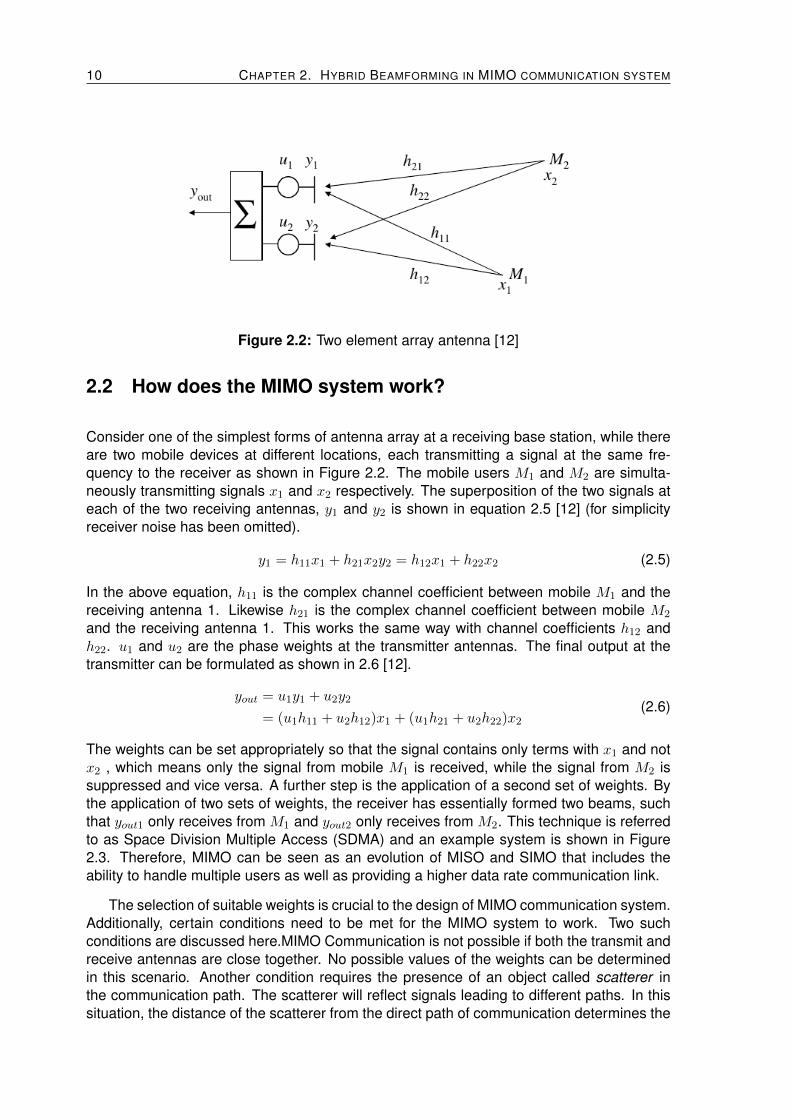
Figure 2.2: Two element array antenna [12]
2.2 How does the MIMO system work?
Consider one of the simplest forms of antenna array at a receiving base station, while thereare two mobile devices at different locations, each transmitting a signal at the same fre-quency to the receiver as shown in Figure 2.2. The mobile users M1 and M2 are simulta-neously transmitting signals x1 and x2 respectively. The superposition of the two signals ateach of the two receiving antennas, y1 and y2 is shown in equation 2.5 [12] (for simplicityreceiver noise has been omitted).
y1 = h11x1 + h21x2y2 = h12x1 + h22x2 (2.5)
In the above equation, h11 is the complex channel coefficient between mobile M1 and thereceiving antenna 1. Likewise h21 is the complex channel coefficient between mobile M2
and the receiving antenna 1. This works the same way with channel coefficients h12 andh22. u1 and u2 are the phase weights at the transmitter antennas. The final output at thetransmitter can be formulated as shown in 2.6 [12].
yout = u1y1 + u2y2
= (u1h11 + u2h12)x1 + (u1h21 + u2h22)x2(2.6)
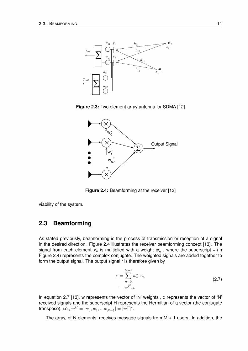
The weights can be set appropriately so that the signal contains only terms with x1 and notx2 , which means only the signal from mobile M1 is received, while the signal from M2 issuppressed and vice versa. A further step is the application of a second set of weights. Bythe application of two sets of weights, the receiver has essentially formed two beams, suchthat yout1 only receives from M1 and yout2 only receives from M2. This technique is referredto as Space Division Multiple Access (SDMA) and an example system is shown in Figure2.3. Therefore, MIMO can be seen as an evolution of MISO and SIMO that includes theability to handle multiple users as well as providing a higher data rate communication link.
The selection of suitable weights is crucial to the design of MIMO communication system.Additionally, certain conditions need to be met for the MIMO system to work. Two suchconditions are discussed here.MIMO Communication is not possible if both the transmit andreceive antennas are close together. No possible values of the weights can be determinedin this scenario. Another condition requires the presence of an object called scatterer inthe communication path. The scatterer will reflect signals leading to different paths. In thissituation, the distance of the scatterer from the direct path of communication determines the
2.3. BEAMFORMING 11
Figure 2.3: Two element array antenna for SDMA [12]
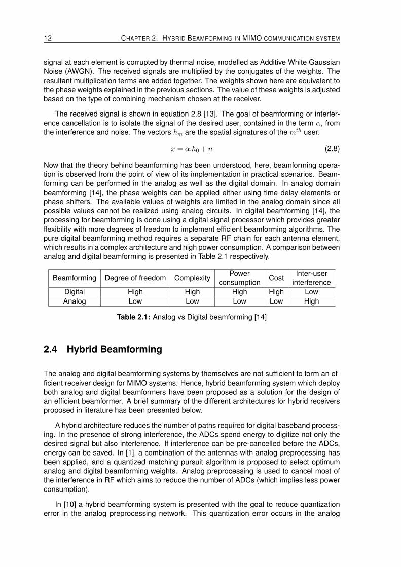
Figure 2.4: Beamforming at the receiver [13]
viability of the system.
2.3 Beamforming
As stated previously, beamforming is the process of transmission or reception of a signalin the desired direction. Figure 2.4 illustrates the receiver beamforming concept [13]. Thesignal from each element xn is multiplied with a weight wn , where the superscript ∗ (inFigure 2.4) represents the complex conjugate. The weighted signals are added together toform the output signal. The output signal r is therefore given by
r =N−1∑n=0
w∗n.xn
= wH .x
(2.7)
In equation 2.7 [13], w represents the vector of ‘N’ weights , x represents the vector of ‘N’received signals and the superscript H represents the Hermitian of a vector (the conjugatetranspose), i.e., wH = [w0, w1, ...wN−1] = [wT ]∗.
The array, of N elements, receives message signals from M + 1 users. In addition, the
12 CHAPTER 2. HYBRID BEAMFORMING IN MIMO COMMUNICATION SYSTEM
signal at each element is corrupted by thermal noise, modelled as Additive White GaussianNoise (AWGN). The received signals are multiplied by the conjugates of the weights. Theresultant multiplication terms are added together. The weights shown here are equivalent tothe phase weights explained in the previous sections. The value of these weights is adjustedbased on the type of combining mechanism chosen at the receiver.
The received signal is shown in equation 2.8 [13]. The goal of beamforming or interfer-ence cancellation is to isolate the signal of the desired user, contained in the term α, fromthe interference and noise. The vectors hm are the spatial signatures of the mth user.
x = α.h0 + n (2.8)
Now that the theory behind beamforming has been understood, here, beamforming opera-tion is observed from the point of view of its implementation in practical scenarios. Beam-forming can be performed in the analog as well as the digital domain. In analog domainbeamforming [14], the phase weights can be applied either using time delay elements orphase shifters. The available values of weights are limited in the analog domain since allpossible values cannot be realized using analog circuits. In digital beamforming [14], theprocessing for beamforming is done using a digital signal processor which provides greaterflexibility with more degrees of freedom to implement efficient beamforming algorithms. Thepure digital beamforming method requires a separate RF chain for each antenna element,which results in a complex architecture and high power consumption. A comparison betweenanalog and digital beamforming is presented in Table 2.1 respectively.
Beamforming Degree of freedom ComplexityPower
consumptionCost
Inter-userinterference
Digital High High High High LowAnalog Low Low Low Low High
Table 2.1: Analog vs Digital beamforming [14]
2.4 Hybrid Beamforming
The analog and digital beamforming systems by themselves are not sufficient to form an ef-ficient receiver design for MIMO systems. Hence, hybrid beamforming system which deployboth analog and digital beamformers have been proposed as a solution for the design ofan efficient beamformer. A brief summary of the different architectures for hybrid receiversproposed in literature has been presented below.
A hybrid architecture reduces the number of paths required for digital baseband process-ing. In the presence of strong interference, the ADCs spend energy to digitize not only thedesired signal but also interference. If interference can be pre-cancelled before the ADCs,energy can be saved. In [1], a combination of the antennas with analog preprocessing hasbeen applied, and a quantized matching pursuit algorithm is proposed to select optimumanalog and digital beamforming weights. Analog preprocessing is used to cancel most ofthe interference in RF which aims to reduce the number of ADCs (which implies less powerconsumption).
In [10] a hybrid beamforming system is presented with the goal to reduce quantizationerror in the analog preprocessing network. This quantization error occurs in the analog
2.4. HYBRID BEAMFORMING 13
phase shifter and amplifier of the analog preprocessing network. The quantized matchingpursuit algorithm is used to find the optimum analog and digital beamforming values aspresented in [1].
In [11] a design framework for hybrid beamforming for multi-cell multiuser massive MIMOsystems over mmWave channels has been presented. This paper presents a new approachfor designing analog beamforming using Kronecker decomposition 1. Kronecker decompo-sition is aimed at removing the constraints put on analog beamforming due to the use ofphase-arrays for obtaining the coefficient values. In addition to these systems, there aremany more hybrid system [15], [16] which have been proposed over recent years to makeMIMO communication more efficient using hybrid beamforming.
The hybrid beamforming receiver (as shown in Figure 1.3) presented in this researchassignment is mainly based on the system in proposed [1]. With this discussion on thedifferent hybrid receiver architectures, in the following sections the concepts which explainthe exact mechanism of working of hybrid beamforming system used in this research havebeen explained.
Minimum Mean Squared Error (MMSE)
Beamforming can be performed under different optimal conditions. In this assignment thefocus is on MMSE algorithm for optimal beamforming. The MMSE [13] algorithm minimizesthe error with respect to a reference signal d(t). In this model, the desired user is assumedto transmit this reference signal, i.e., α = βd(t), where β is the signal amplitude and d(t) isknown to the receiving base station. The MMSE tries to find the weights w of the beamformerthat minimize the average power in the error signal i.e. the difference between the referencesignal and the output signal obtained using equation 2.7. The equation which tries to findthe optimum value for weights w using MMSE has been shown in equation 2.9 [13].
The calculation of the mean square error value has been shown in equations 2.10 [13] and2.11 [13]. Finding the minimal value of w as shown in equation 2.9 requires differentiationw.r.t. wH . This results in the value of w as shown in equation 2.12 [13]. This solution isknown as the Wiener Filter. Here, wMMSE denotes the optimal beamformer value.
wMMSE = R−1.rxd (2.12)
R is the covariance matrix given by the equation, R = E[x.xH ]
1Kronecker decomposition is an operation on two matrices of arbitrary size which results in a block matrix.
14 CHAPTER 2. HYBRID BEAMFORMING IN MIMO COMMUNICATION SYSTEM
The MMSE technique minimizes the error with respect to a reference signal. Therefore, itdoes not require knowledge of the spatial signature (channel information), but does requireknowledge of the transmitted signal. This is an example of a training based scheme: thereference signal acts to train the beamformer weights.
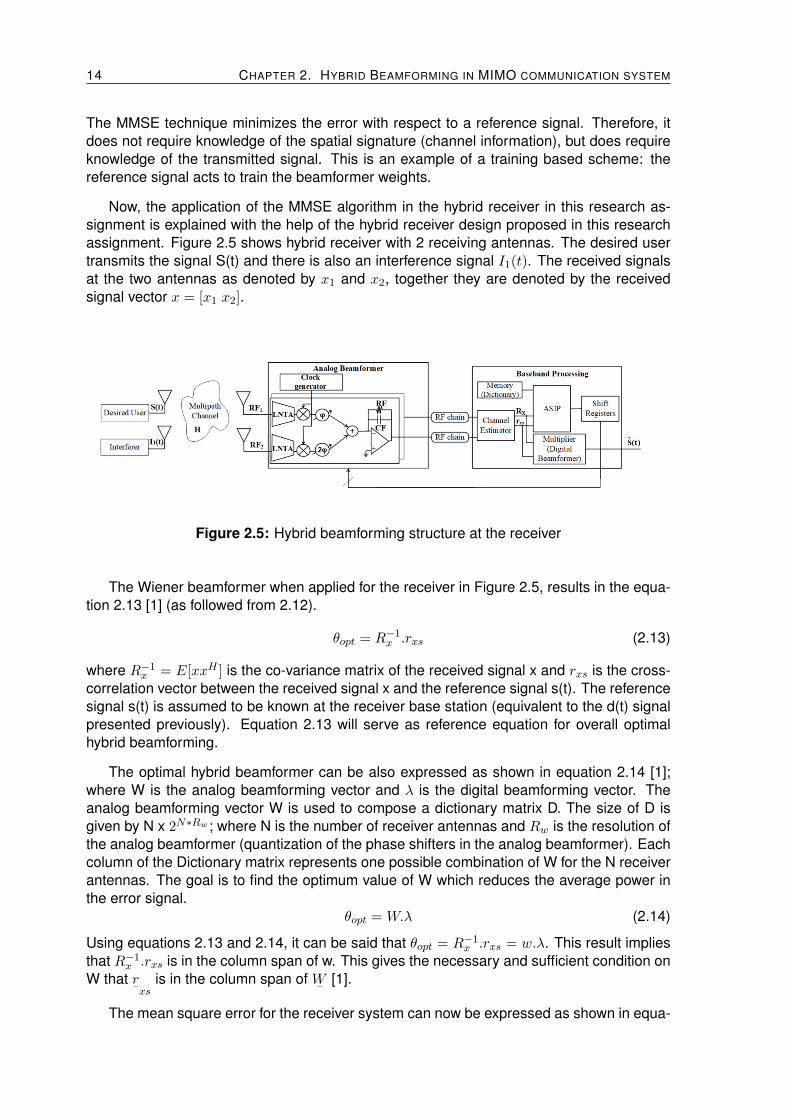
Now, the application of the MMSE algorithm in the hybrid receiver in this research as-signment is explained with the help of the hybrid receiver design proposed in this researchassignment. Figure 2.5 shows hybrid receiver with 2 receiving antennas. The desired usertransmits the signal S(t) and there is also an interference signal I1(t). The received signalsat the two antennas as denoted by x1 and x2, together they are denoted by the receivedsignal vector x = [x1 x2].
Figure 2.5: Hybrid beamforming structure at the receiver
The Wiener beamformer when applied for the receiver in Figure 2.5, results in the equa-tion 2.13 [1] (as followed from 2.12).
θopt = R−1x .rxs (2.13)
where R−1x = E[xxH ] is the co-variance matrix of the received signal x and rxs is the cross-
correlation vector between the received signal x and the reference signal s(t). The referencesignal s(t) is assumed to be known at the receiver base station (equivalent to the d(t) signalpresented previously). Equation 2.13 will serve as reference equation for overall optimalhybrid beamforming.
The optimal hybrid beamformer can be also expressed as shown in equation 2.14 [1];where W is the analog beamforming vector and λ is the digital beamforming vector. Theanalog beamforming vector W is used to compose a dictionary matrix D. The size of D isgiven by N x 2N∗Rw ; where N is the number of receiver antennas and Rw is the resolution ofthe analog beamformer (quantization of the phase shifters in the analog beamformer). Eachcolumn of the Dictionary matrix represents one possible combination of W for the N receiverantennas. The goal is to find the optimum value of W which reduces the average power inthe error signal.
θopt =W.λ (2.14)
Using equations 2.13 and 2.14, it can be said that θopt = R−1x .rxs = w.λ. This result implies
that R−1x .rxs is in the column span of w. This gives the necessary and sufficient condition on
W that r¯xs
is in the column span of W¯
[1].
The mean square error for the receiver system can now be expressed as shown in equa-
2.4. HYBRID BEAMFORMING 15
tion 2.15 [10], where s1[k] is the discretized version of the signal transmitted by the desireduser (S(t)) and x[k] represents the discretized version of the receiver signal(x).
For any value W and the corresponding optimal λ = (WHRxW )−1WHrxs, the MSE equationin 2.15 can be re-written as shown in equation 2.16 [1].
MSE = 1− rHxsW (WHRxW )−1WHrxs
= 1− rHxsPWrxs(2.16)
In equation 2.16, PW is the orthogonal projection matrix given by PW = W(WHW)−1WH
and W = R12xW is the whitened analog beamforming vector. The solution W0 which satisfies
the MMSE equation is given by equation 2.17 [1].
W0 = argmaxW
rHxsPWrxs (2.17)
The MSE presented in equation 2.16 will have minimum value when the term rHxsPWrxs hasthe maximum value for a given value of W. This implication has been presented in equation2.18 [1].
W = arg maxW∈D
rHxsPWrxs
= arg maxW∈D
||PWrxs||2(2.18)
These results are equivalent to equation 2.19 [1].
W = arg minW∈D
||(I − PW)rxs||2
= arg minW∈D
||rxs −W(WHW)WH ||2
= ||rxs −Wλ||2
(2.19)
To reduce the complexity, the columns of W are selected one-by-one. The quantized match-ing pursuit algorithm [1] is used tp recursively choose the dictionary elements to obtain thebest approximation of the input vector (rxs in this case). Following this algorithm, the problemreduces to finding the solution for the equation 2.20 [1].
wopt = arg maxwi∈D
|wHi rxs|||wi||
(2.20)
In equation 2.20, wopt refers to the optimum whitened analog beamformer value, wi refersto the column i of the whitened dictionary D
¯of whitened analog beamformer W, ||wi|| refers
to the norm of the whitened column vector wi. The process of calculating the value of w¯ opt
which maximises the value of right hand side in equation 2.20 has been termed as SearchAlgorithm in the context of this assignment.
16 CHAPTER 2. HYBRID BEAMFORMING IN MIMO COMMUNICATION SYSTEM
The Search algorithm can be summarized as follows: Given an input covariance matrixCrr , a cross-correlation vector Crxi , and a dictionary of quantized analog beamformingvectors D.
• Transform the analog beamforming vector W to the whitened matrix W¯
.
• Compute the value of w¯ i
which gives the maximum value of right hand side in equation2.20.
2.5 Related Work
Chapter 1 provides the information about the problem statement that is tackled in this thesisassignment and the previous sections provides the necessary background information tounderstand this problem statement. In this section, some of the ASIP implementations inMIMO communication systems are discussed.
In [17] an ASIP is used for implementing a flexible Minimum Mean Square Error-InterferenceCanceller (MMSEIC) linear equalizer for MIMO turbo-equalization applications. The pro-posed 16-bit ASIP has an Single Instruction Multiple Data (SIMD) architecture with a spe-cialized instruction set and 7 stage pipeline. The special instruction set architecture supportscomplex numbered matrix operations. The ASIP is mainly composed of Matrix RegisterBanks (MRB), Complex Arithmetic Unit (CAU) and Control Unit (CU) along with a memoryinterface. The MRBs are used to store complex number in two 16-bit registers. The CAUhas the computational resources to perform 4 concurrent complex additions, subtractions,complex conjugation and multiplications. The ASIP is synthesized using 90 nm technologyfor a frequency 546 MHz.
In [18], 32-bit ASIPs are used for realizing channel equalization algorithm for MIMOsystem in Wide Code Division Multiple Access (WCDMA) downlink. The ASIPs are designedon the principle of Transport Triggered Architecture (TTA) 2. Similar to ASIP presentedin [17], here also there are Special Functional Unit (SFU)s which deal with the handling ofcomplex number processing. The SFUs are evidenced to provide significant reduction in bustraffic and connection between buses in the proposed ASIPs. Another ASIP implementationis proposed in [19] and [20] where it is used realize a low complexity iterative precoder formulti user MIMO.
[21] presents an ASIP design used for implementing singular value decomposition inMIMO systems. The processor has special instructions for complex value multiplication,vector norm computation and concurrent matrix processing operations. Singular value de-composition is used for beamforming in MIMO system in [21] hence the architectural choicesin this paper can serve as a reference for the design methodology as expected in this the-sis assignment. However, the instruction encoding is quite wide given that a 102-bit wideinstruction bus is used. In addition to complex arithmetic handling as seen in the previousdesigns, this design also provides special hardware to perform floating point arithmetic.
Reconfigurable ASIPs have also been proposed in MIMO systems as seen in [22]. The
2A TTA is a kind of processor design in which programs directly control the internal transport buses of aprocessor. Computation happens as a side effect of data transports: writing data into a triggering port of afunctional unit triggers the functional unit to start a computation
2.6. ROLE OF THE ASIP BASEBAND PROCESSOR 17
reconfigurable ASIP (termed as rASIP) is composed of a Coarse Grain ReconfigurableArchitecture (CGRA) along with a processor. The reconfigurability of the processor is ex-ploited by implementing 4 MIMO detection algorithms based on the requirement of the sys-tem. The detection algorithm are : zero forcing, linear MMSE, MMSE and Marko ChainMonte Carlo (MCMC) based detection algorithm. Along the same lines [23] proposes a sys-tem where the processor is configured to perform multiple tasks. These tasks are disjointprocesses viz. beamforming and channel feedback. ASIP implementation saves resourcessince it can be used to implement multiple tasks on the same platform as long as these tasksare multiplexed in time. The instruction set is designed such that many other tasks such asencryption-decryption, checksum generation etc. can also be performed without any addi-tional hardware costs. The baseband processor in this thesis assignment can be designedalong similar lines i.e. with an instruction set which can support multiple operations whichare generally a part of MIMO communication systems.
The systems presented here are by no means exhaustive and many more implementa-tions might be present. The operations implemented in the systems presented earlier aresimilar to the operations expected to be performed in this assignment. Hence, these designshave been considered. The investigation to determine ASIP implementation in MIMO sys-tems has revealed that an ASIP design for computing optimal coefficient values in a hybridbeamforming system (as shown in Figure 1.3) has not yet been proposed.
2.6 Role of the ASIP Baseband processor
The expected design of the baseband processing block as a part of the hybrid beamformingsystem has been shown in Figure 2.6. The figure essentially consists of 5 blocks viz. theDictionary, the Estimator, the ASIP, the Multiplier(Digital Beamformer) and the Shift registersblock. The function of each block is explained as follows:
• Dictionary: This block comprises of all possible values of the quantized analog beam-forming coefficients. For a system with N antennas and a resolution of Rw (resolutionof the phase shifters in the analog beamformer), the dictionary consists of N ∗2Rw pos-sibilities. As the number of antennas and their corresponding resolution will increase,the size of the dictionary will increase exponentially. Considering this, at the beginningof this assignment it was decided to store the dictionary in an external memory unitwhich is interfaced with the ASIP.
• Estimator : The calculation of the optimum analog beamformer requires the calculationof the cross-correlation matrix Crx and the corresponding whitened matrix value C
¯ rx.
This operation has been assigned to the estimator block. This block is expected tobe an Application Specific Integrated Circuit (ASIC) dedicated for this purpose sincecalculation of cross-correlation values and whitened matrix values for complex valuesis a computationally demanding task and it is also required to be fast (in terms ofcalculation speed). In addition to this, this block will also calculate the co-variancevalue of the received signal. This block takes input from the RF chain to perform thementioned operations. It will also be provided with the reference signal value which isassumed to be known at the receiver.
• ASIP: This block is expected to perform the task of determining the optimum analog
18 CHAPTER 2. HYBRID BEAMFORMING IN MIMO COMMUNICATION SYSTEM
beamformer coefficient values following the search algorithm 3 explained previously. Itwill take input values from the Dictionary and Estimator blocks and the output of thisblock is given back to the analog beamformer.
• Multiplier (Digital Beamformer): This block is expected to perform the digital beam-forming on the signals obtained from the RF chain in the baseband domain. The ASIPis not involved in the digital beamforming operation.
• Shift registers: The ASIP will produce vector values at the output. These values needto be converted to bit patterns which will turn on/off the switches in the analog beam-former to achieve different coefficient values. The Shift registers deliver this bit patternto the analog beamformer. The conversion operation can either be performed in theASIP or in the shift register block.
Figure 2.6: Typical expected design of the baseband processing block of hybrid receiver
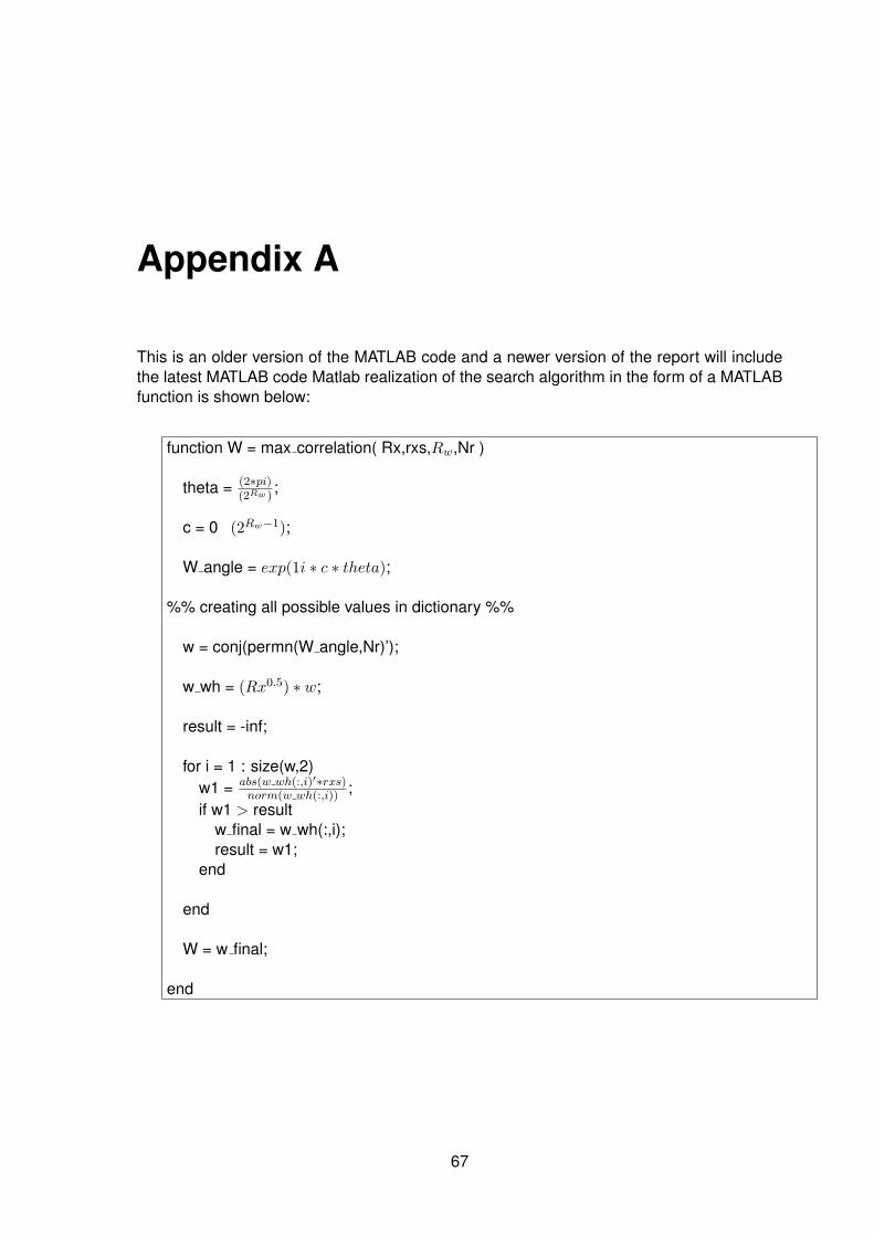
3Matlab Implementation snippet available in Appendix A
Chapter 3
Choice of Instruction SetArchitecture
An Instruction Set Architecture (ISA) represents a abstract computer model. Realization ofISA is termed as implementation. Multiple implementations of a computer model are possi-ble based on variation in performance, size and cost etc. The ISA acts as the mediating layerbetween hardware and software. There are different variants of ISAs : licensed, custom oropen source. In this research assignment the focus is on the use of open source instructionset architectures.
The cornerstone of ASIP design is the customization of the instruction set with respectto a given application. In that sense, a completely new instruction set can be developedwith the search algorithm at its focus. On the other hand, if the foundation of the ASIP isbuilt on existing open source architectures, it ensures certain support on the software end,insights from the community of users and developers, etc. There are several processor (orcores) and system on chip platforms with hardware and software support based on the opensource instruction set architectures readily available on the open source platforms. Theseare a few reasons because of which the ASIP architecture is chosen to be developed onan existing open source instruction set architecture. A few of these open source ISAs arediscussed in this chapter.
The choice of the right open source architecture depends on several factors such asthe support provided by the developers’ and users’ community, available software tools forproper experimentation (for example instruction set simulator), scope and ease of instructionset extension. etc. Based on these criteria, selection of the reference open source archi-tecture can be performed. The motivation behind this selection is also discussed in furthersections of this chapter.
In the next section, the key features of three ISAs are discussed. They are : OpenRISC,UltraSPARC and RISC-V.
19
20 CHAPTER 3. CHOICE OF INSTRUCTION SET ARCHITECTURE
3.1 OpenRISC
The OpenRISC (or OpenRISC 1000) [24] architecture is an open source RISC based archi-tecture. It targets the medium and high performance networking and embedded computerenvironments. Some of its important features are :
• A linear, 32-bit or 64-bit logical address space with implementation-specific physicaladdress space.
• Simple and uniform-length instruction formats featuring different instruction set exten-sions:
– OpenRISC Basic Instruction Set (ORBIS32/64) with 32-bit wide instructions alignedon 32-bit boundaries in memory and operating on 32- and 64-bit data
– OpenRISC Vector/DSP extension (ORVDX64) with 32-bit wide instructions alignedon 32-bit boundaries in memory and operating on 8-, 16-, 32- and 64- bit data
– OpenRISC Floating-Point extension (ORFPX32/64) with 32-bit wide instructionsaligned on 32-bit boundaries in memory and operating on 32- and 64-bit data
• Optional branch delay slot for keeping the pipeline as full as possible
• A flexible architecture definition that allows certain functions to be performed either inhardware or with the assistance of implementation-specific software.
• Fast context switch support in register set, caches, and memory management units.
• Memory is byte-addressed with half word accesses aligned on 2-byte boundaries, sin-gle word accesses aligned on 4-byte boundaries, and double word accesses alignedon 8-byte boundaries.
• The OpenRISC architecture specifies a weakly ordered memory model for uniproces-sor and shared memory multiprocessor systems. This model has the advantage of ahigher-performance memory system but places the responsibility for strict access or-dering on the programmer (through special instructions which specify no reordering).
3.2 UltraSPARC
UltraSPARC architecture [25] is another RISC based open source ISA wherein SPARCstands for Scalable Processor Architecture. Some of the features of SPARC architectureare:
• The SPARC Architecture supports 32-bit and 64-bit integer and 32 bit, 64 bit, and 128bit floating-point as its principal data types.
• The 32-bit and 64-bit floating-point types conform to IEEE Std 754-1985. The 128 bitfloating-point type conforms to IEEE Std 1596.5-1992.
• It supports a linear 64-bit address space with 64-bit addressing. The instructions are32-bit wide instructions and are aligned on 32-bit boundaries in memory. Only loadand store instructions access memory and perform I/O.
3.3. RISC-V 21
• The architecture defines general-purpose integer, floating-point, and special state/statusregister instructions, all encoded in 32 bit wide instruction formats.
• The load/store instructions address a linear, 264-byte virtual address space.
• The instruction set comes with many extensions, including the Virtual Instruction Set(VIS) for “vector” i.e. SIMD operations.
An important highlight of this architecture is the support for Chip Multi-Threaded (CMT)technology. CMT is an application of parallel processing. It can be seen as being sim-ilar to software multi-threading where multiple processor activities can be done in asingle process. The only difference is that CMT is hardware-based so that the pro-cessor handles the different threads instead of the software. The key advantage ofthis compared to older processor technologies is improved throughput. The SPARCarchitecture supports CMT design by providing a control architecture.
3.3 RISC-V
The name RISC-V was chosen to represent the fifth major RISC ISA design from UC Berke-ley (RISC-I , RISC-II, SOAR, and SPUR were the first four). RISC-V ISA [26] allows efficientimplementation of different particular microarchitecture styles (e.g., microcoded, in-order,decoupled, out-of-order) and different implementation technologies (e.g., full-custom, ASIC,FPGA) combinations.
• The ISA is separated into a small base integer ISA, usable by itself as a base for cus-tomized accelerators or for educational purposes, and optional standard extensions,to support general-purpose software development.
– Each base integer instruction set is characterized by the width of the integer reg-isters and the corresponding size of the user address space. There are 4 baseinstruction set variants: RV32I, RV32E, RV64I and RV128I.
– The RV32E is a reduced version of the RV32I ISA especially aimed at embeddedsystem applications. There are a lot more standard extensions for e.g. extensionwhich supports compressed instruction format RV32C. The naming conventionfor the base instruction set, standard and custom extensions can be found in [26].
• Support for the revised 2008 IEEE-754 floating-point standard.
• RISC-V supports extensive user-level ISA extensions and specialized variants.
• Both 32-bit and 64-bit address space variants for applications, operating system ker-nels, and hardware implementations.
• It supports highly-parallel multi core implementations, including heterogeneous multi-processors.
• Optional variable-length instructions to both expand available instruction encoding spaceand to support an optional dense instruction encoding for improved performance, staticcode size, and energy efficiency.
22 CHAPTER 3. CHOICE OF INSTRUCTION SET ARCHITECTURE
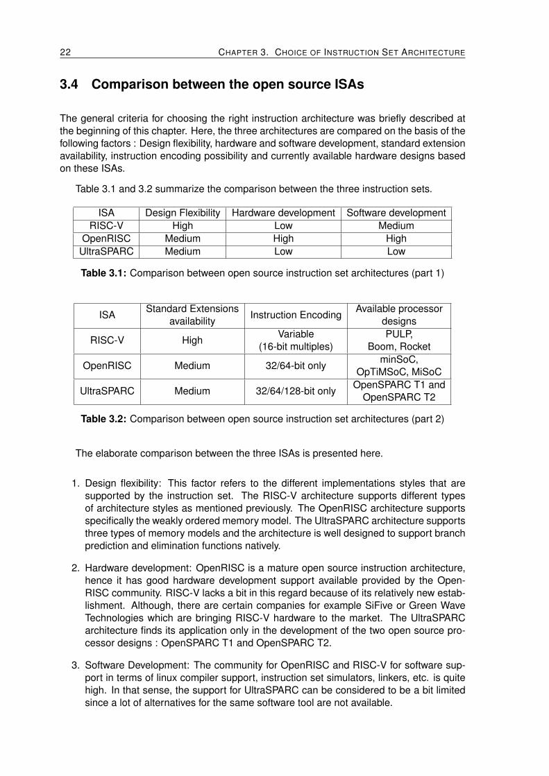
3.4 Comparison between the open source ISAs
The general criteria for choosing the right instruction architecture was briefly described atthe beginning of this chapter. Here, the three architectures are compared on the basis of thefollowing factors : Design flexibility, hardware and software development, standard extensionavailability, instruction encoding possibility and currently available hardware designs basedon these ISAs.
Table 3.1 and 3.2 summarize the comparison between the three instruction sets.
ISA Design Flexibility Hardware development Software developmentRISC-V High Low Medium
OpenRISC Medium High HighUltraSPARC Medium Low Low
Table 3.1: Comparison between open source instruction set architectures (part 1)
ISAStandard Extensions
availabilityInstruction Encoding
Available processordesigns
RISC-V HighVariable
(16-bit multiples)PULP,
Boom, Rocket
OpenRISC Medium 32/64-bit onlyminSoC,
OpTiMSoC, MiSoC
UltraSPARC Medium 32/64/128-bit onlyOpenSPARC T1 and
OpenSPARC T2
Table 3.2: Comparison between open source instruction set architectures (part 2)
The elaborate comparison between the three ISAs is presented here.
1. Design flexibility: This factor refers to the different implementations styles that aresupported by the instruction set. The RISC-V architecture supports different typesof architecture styles as mentioned previously. The OpenRISC architecture supportsspecifically the weakly ordered memory model. The UltraSPARC architecture supportsthree types of memory models and the architecture is well designed to support branchprediction and elimination functions natively.
2. Hardware development: OpenRISC is a mature open source instruction architecture,hence it has good hardware development support available provided by the Open-RISC community. RISC-V lacks a bit in this regard because of its relatively new estab-lishment. Although, there are certain companies for example SiFive or Green WaveTechnologies which are bringing RISC-V hardware to the market. The UltraSPARCarchitecture finds its application only in the development of the two open source pro-cessor designs : OpenSPARC T1 and OpenSPARC T2.
3. Software Development: The community for OpenRISC and RISC-V for software sup-port in terms of linux compiler support, instruction set simulators, linkers, etc. is quitehigh. In that sense, the support for UltraSPARC can be considered to be a bit limitedsince a lot of alternatives for the same software tool are not available.
3.4. COMPARISON BETWEEN THE OPEN SOURCE ISAS 23
4. Number of Standard Extensions available: All these instruction set architectures havedifferent types of standard extensions already available. RISC-V is the instructionset architecture with a lot of extensions already standardized, for example, an atomicextension. Such type of standardization for different extensions directly implies avail-ability of software support. At the same time, the usage/requirement of a particularextension is also an application dependent factor.
5. Instruction Encoding: The RISC-V ISA provides the most flexible instruction encodingoption by supporting any instruction encoding format which is multiple of 16. Thismeans based on the design requirements it can support a varying range of instructionencoding formats from compressed instruction formats to VLIW formats.
6. Available processor designs: This last factor lists the available implementations of thethree instruction sets.
From this discussion it can be gathered that RISC-V provides high design flexibility alongwith good software development support. This is due to its modular design, which featuresa common base of roughly 40 integer instructions (I) that all cores must implement, withample opcode space left over to support optional extensions, of which the most canonicalhave already been standardized.
The RISC-V instruction set architecture allows for easy integration of user defined cus-tom instructions in the existing base or standard extensions sets. This allows to developdesign of the core such that specific speed or energy efficiency can be achieved in certainoperations. Along with support for user level ISA extension, a key feature of this instructionset is the support for compressed instructions. The existing standard custom instruction setsupports the compressed format for some basic instructions like add, sub etc. The advan-tage of using such compressed instructions is that it reduces the length of the program code;saving memory and power at the same time. This feature is not found in OpenRISC and Ul-traSPARC architectures. However, whether a compressed instruction format is needed waskept an open question.
Additionally, the user base for RISC-V is increasing exponentially. There is ample supportprovided by the members of the RISC-V foundation and the community of programmers anddevelopers. Tech giants such as Qualcomm, Western digital and many others are investingin RISC-V as an open source alternative to licensed ISAs such as ARM.
Hence, RISC-V has been chosen as the reference open source architecture upon whichthe instruction set of the ASIP will be developed.
24 CHAPTER 3. CHOICE OF INSTRUCTION SET ARCHITECTURE
Chapter 4
Processor Modeling tool and flow ofdesign
In this Chapter, the tool used to design the ASIP is discussed along with the design flowfollowed for processor modeling in this tool.
4.1 Processor Modeling tool
The Synopsys ASIP designer has been chosen to design the ASIP for the hybrid receiver.The overall tool flow has been shown in Figure 4.1.
Figure 4.1: Synopsys ASIP designer tool flow [9]
25
26 CHAPTER 4. PROCESSOR MODELING TOOL AND FLOW OF DESIGN
ASIP Designer supports the following features:
• Modeling of ASIP instruction set architectures in the nML processor description lan-guage. nML is a high-level definition language for describing a processor architectureand instruction set.
• Once, the processor architecture has been defined using nML, the tool generates theentire Software Development Kit (SDK). The SDK comprises of the Compiler, assem-bler, linker, Instruction Set Simulator (ISS), etc. Using the ISS the simulation for adesired algorithm (in C/C++) can be performed. Based on the results obtained re-finement can be performed in the processor model. This process is known as thecompiler-in-the-loop architectural exploration.
• The SDK comprises of the following elements:
– An optimizing compiler which provides efficient code generation and, quick andautomatic retargetability to new ASIP architectures. The compiler supports C (op-tionally extended with user-defined data types and operators using C++ classesand function overloading), C++, and OpenCL C (OpenCL kernel language). Thecompiler can cope well with architectural peculiarities of DSP cores. It sup-ports instruction-level and data-level parallelism, deeply pipelined instructions,specialized arithmetic functions, custom data-types, specialized address genera-tion units, heterogeneous register structures, and various degrees of instructionencoding (ranging from VLIW to highly encoded instruction sets).
– A linker that builds an executable file from separately compiled Elf/Dwarf objectfiles for different C functions.
– An assembler and disassembler that translates machine code from assembly intobinary format and back.
– A fast ISS, offering both cycle-accurate and instruction-accurate abstraction levelsgenerated from the same nML model, and easy integration into cycle-accurateand transaction-level virtual prototypes.
– A flexible (multicore) debugger, which can be used in connection to both ISSs andon-chip debug hardware (via JTAG).
– Multi-faceted profiling capabilities to analyze the instruction-set architecture forhot-spots and to drive the architectural optimization process.
• The tool also automatically generates a power and area efficient hardware implemen-tation of each ASIP, in synthesizable Verilog or VHDL. The RTL design can be verifiedvia simulation and again refinement can be performed in the processor model. Thisprocess is known as the synthesis-in-the-loop architectural exploration
A JTAG interface and a debug controller can optionally be generated, to support on-chip debugging.
• The automatic generation of ASIP-specific test programs in C and assembly codeallows extensive verification of the ASIP.
• Another important feature of the ASIP Designer tools is that it comes with a widerange of example ASIP designs, with highly differentiating architectures provided innML source code.
4.2. PROCESSOR MODEL DESIGN FLOW 27
The compiler-in-the-loop and synthesis-in-the-loop architectural exploration provided by theASIP designer make it the ideal choice for designing the target ASIP in this assignment.Along with these architectural exploration processes the example processors that are pro-vided are also an added advantage. These processor models can be used as referenceswhile making different design decisions during the ASIP development. Hence, the SynopsysASIP designer is chosen as the tool suite for the development of the ASIP in this researchassignment. The next section explains different steps involved in the design of the processormodel.
4.2 Processor model design flow
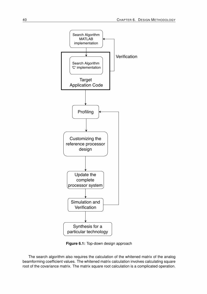
The flow chart shown in Figure 4.2 shows the different design steps that must be taken bythe user to model the processor in Synopsys ASIP design tool.
Figure 4.2: Design Steps for processor modelling in Synopsys ASIP designer
The steps are explained as follows:
28 CHAPTER 4. PROCESSOR MODELING TOOL AND FLOW OF DESIGN
• Primitive Declaration: The first step is the declaration of user-defined processor spe-cific data types and functions. These data types are defined as C++ classes and func-tions respectively. They are defined in the <processor>.h file in the primitive names-pace.
• nML model: The data path of the processor model is defined in the nML model. Thismodel can be broken down into 2 components: structural skeleton and instruction setdescription. The structural skeleton comprises of storage elements, functional units,registers, wires, etc. The instruction set description consists of grammar rules whichdefine the behavior of the data path. The nML model uses the primitive types andfunctions for defining the data path.
• PDG model: The PDG model is written in Primitive Definition and Generation (PDG)language which is based on “C”. It has operators from “C” and some from “Verilog”. Allthe primitive functions declared in the <processor>.h file must be defined here. Thecontroller of the processor model is also defined in the PDG model. The I/O interfacingis also done using PDG.
• Compiler Header File: The final step in processor design is writing the compiler headerfile. The mapping of the C built-in types and operator to primitive processor types andfunctions is performed in this file. Along with these, additional processor optimizationdirectives and specification of the subroutine call convention is also done in this step.
• Native Header File : This file is automatically generated by the ASIP designer tool fromthe compiler header file. The tool maps custom data-types and functions from theapplication code to data-types and functions that the host machine can understand.This file plays a quite an important role in the verification on the application level.The C code is compiled for the host and target machines and then verification can beperformed by comparison.
Once all the design steps have been performed by the user the entire processor modelcan be said to be available. This resultant model represents the processor model shownon the left side in Figure 4.1. The processor model is used by the Synopsys ASIP de-signer to generate the SDK. Once the SDK is available, verification and different tests canbe run on the processor. Different C/C++ applications can be run on the processor to per-form required evaluation of the processor performance, for instance, running the CoremarkBenchmark [27]. Using the compiler-in-the-loop technology, refinement based on verifica-tion and performance evaluation can be implemented and results seen immediately via thesimulator. Once the user is satisfied with the performance characteristics of the processor,the synthesis of the processor can be performed using the Synopsys ASIP Designer. Thesynthesis-in-the-loop technology can be used to perform finer refinement in the processormodel. In this way, the processor modeling can be performed using Synopsys ASIP de-signer.
4.2.1 In-Depth insight into each step of processor model design flow
To understand the processor model design flow steps more clearly and gain better perspec-tive about the complexity involved in processor design in the Synopsys ASIP designer, herein this subsection, each step from Figure 4.2 is explained with examples.
4.2. PROCESSOR MODEL DESIGN FLOW 29
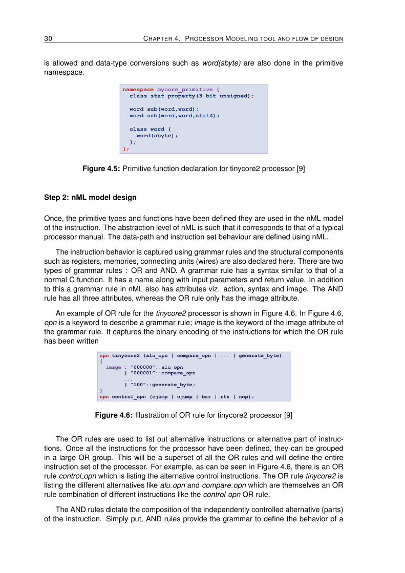
Step 1: Primitive Declaration
As stated previously, all the primitives are declared in the <processor>.h file called the prim-itive processor header file (where processor refers to actual given name of the ASIP). Insidethe primitive processor header file, all the primitive data types and functions are declared.Primitive declaration is performed because the compiler maps C types and operators ontoprimitive types and functions.A sample namespace for tinycore21 processor is shown in Figure 4.3.
Figure 4.3: Primitive namespace for tinycore2 processor [9]
Primitive data-types are specified using a C++ class declaration inside the primitivenamespace. The sample primitive types declared for processor tinycore2 are shown inFigure 4.4. The primitive data-type word can then be used to define registers or inputs tofunctional units of 16-bit signed type. The primitive data-type pmtype will be used to definethe type of program memory data; sbyte will be used to define signed 8-bit values.
Figure 4.4: Primitive data type declaration for tinycore2 processor [9]
Similarly, primitive functions are also declared in the primitive namespace. An instructionis mapped to a primitive function (either directly or indirectly). Following this, the structure ofthe primitive function will be such that: the operands in the instruction being added becomethe input arguments for the function, and the output of the function will be the resultantoperand of the instruction. Additionally, the primitive function might have additional input oroutput status signals based on the type of instruction that will be mapped to it. For example,an extra input argument will be required when dealing with control signals which might notbe directly visible in the instruction being added.In Figure 4.5, for the primitive function wordsub(word,word,stat&) stat is an additional signal which will be used to indicate the statusof the subtraction operation. From this figure, it can also be seen that function overloading
1The tinycore2 is one of the example processor models provided alongside the Synopsys ASIP designer toolsuite
30 CHAPTER 4. PROCESSOR MODELING TOOL AND FLOW OF DESIGN
is allowed and data-type conversions such as word(sbyte) are also done in the primitivenamespace.
Figure 4.5: Primitive function declaration for tinycore2 processor [9]
Step 2: nML model design
Once, the primitive types and functions have been defined they are used in the nML modelof the instruction. The abstraction level of nML is such that it corresponds to that of a typicalprocessor manual. The data-path and instruction set behaviour are defined using nML.
The instruction behavior is captured using grammar rules and the structural componentssuch as registers, memories, connecting units (wires) are also declared here. There are twotypes of grammar rules : OR and AND. A grammar rule has a syntax similar to that of anormal C function. It has a name along with input parameters and return value. In additionto this a grammar rule in nML also has attributes viz. action, syntax and image. The ANDrule has all three attributes, whereas the OR rule only has the image attribute.
An example of OR rule for the tinycore2 processor is shown in Figure 4.6. In Figure 4.6,opn is a keyword to describe a grammar rule; image is the keyword of the image attribute ofthe grammar rule. It captures the binary encoding of the instructions for which the OR rulehas been written
Figure 4.6: Illustration of OR rule for tinycore2 processor [9]
The OR rules are used to list out alternative instructions or alternative part of instruc-tions. Once all the instructions for the processor have been defined, they can be groupedin a large OR group. This will be a superset of all the OR rules and will define the entireinstruction set of the processor. For example, as can be seen in Figure 4.6, there is an ORrule control opn which is listing the alternative control instructions. The OR rule tinycore2 islisting the different alternatives like alu opn and compare opn which are themselves an ORrule combination of different instructions like the control opn OR rule.
The AND rules dictate the composition of the independently controlled alternative (parts)of the instruction. Simply put, AND rules provide the grammar to define the behavior of a
4.2. PROCESSOR MODEL DESIGN FLOW 31
single instruction. This is done by defining 3 attributes of the AND rule: action, syntax andimage. The register transfer behavior of the instruction will be written in the action attribute.The primitive functions and data types defined in the primitive namespace are used in theaction attribute. The syntax attribute is used to define assembly view of the instruction. Theimage attribute is used to define the binary encoding, just like in the case of OR rule. Figure4.7 shows an example of the AND rule for the tinycore2 processor.
Figure 4.7: Illustration of AND rule for tinycore2 processor [9]
Figure 4.7 shows the AND rule alu opn with 3 parameters (op, a, b) as input argumentswhich are used in the action attribute. In the action attribute the order of the statements isnot important just like while using a hardware description language. The keyword stage E1refers to first execution stage in the pipeline stages of the tinycore2 processor. In this way,the stage by stage execution of the instruction in the pipeline of the processor can also bedefined. aluA = R[a] refers to the reading of the register file at address a. Additionally, add,sub, band, bor are the primitive functions defined for processor tinycore2.
In the presence of a pipelined processor hazards are introduced. These hazards canbe managed using nML image attribute. Keyword cycles in the image attribute is used toindicate the number of clock cycles for which the pipelined must be stalled. An example ofsuch hazard management is shown in Figure 4.8. In this case, when the condition jumpinstruction is encountered during program execution, the newly fetched instruction will notbe executed for 3 cycles.
Figure 4.8: Image attribute changes for hazard management for tinycore2 processor [9]
In addition to this, hazard rules are also written separately as a part of the nML model to
32 CHAPTER 4. PROCESSOR MODELING TOOL AND FLOW OF DESIGN
ensure proper instruction execution. These hazard rules can either use software stalls,hardwarestalls or bypass forwarding to achieve the necessary stalling.
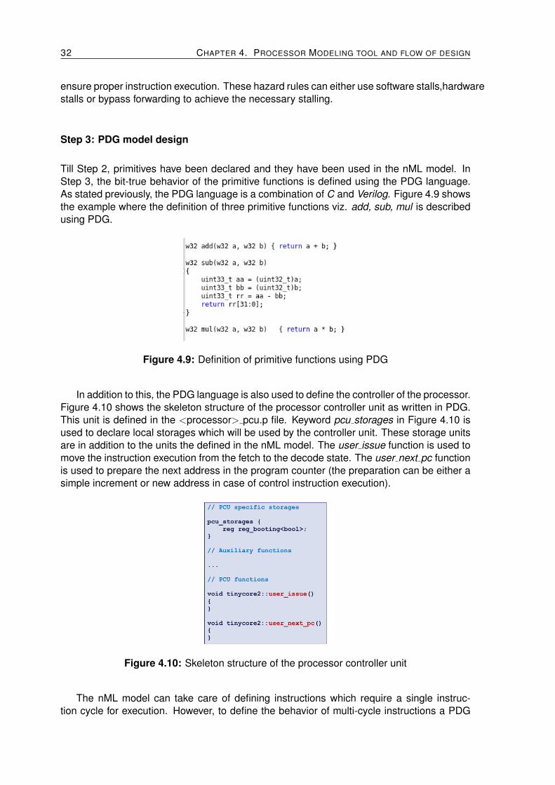
Step 3: PDG model design
Till Step 2, primitives have been declared and they have been used in the nML model. InStep 3, the bit-true behavior of the primitive functions is defined using the PDG language.As stated previously, the PDG language is a combination of C and Verilog. Figure 4.9 showsthe example where the definition of three primitive functions viz. add, sub, mul is describedusing PDG.
Figure 4.9: Definition of primitive functions using PDG
In addition to this, the PDG language is also used to define the controller of the processor.Figure 4.10 shows the skeleton structure of the processor controller unit as written in PDG.This unit is defined in the <processor> pcu.p file. Keyword pcu storages in Figure 4.10 isused to declare local storages which will be used by the controller unit. These storage unitsare in addition to the units the defined in the nML model. The user issue function is used tomove the instruction execution from the fetch to the decode state. The user next pc functionis used to prepare the next address in the program counter (the preparation can be either asimple increment or new address in case of control instruction execution).
Figure 4.10: Skeleton structure of the processor controller unit
The nML model can take care of defining instructions which require a single instruc-tion cycle for execution. However, to define the behavior of multi-cycle instructions a PDG
4.2. PROCESSOR MODEL DESIGN FLOW 33
model is defined. In such case, the nML action will only be used to map the primitive on amulti-cycle functional unit. More on multi-cycle functional units and their implementation isexplained in Chapter 7.
Step 4: Writing the compiler header file
The definitions for mapping the C built-in types and operators to the processor primitive datatypes and functions is done in the compiler header file. The <processor> chess.h is themain compiler header file and it includes a collection of different header files based on theC data types viz. <processor> int.h, <processor> float.h, <processor> double.h etc. Foreach C data type, the operators and data types are mapped to primitive types and functions.
Figure 4.11: Mapping of C operator onto primitive function
Figure 4.11 shows an example of mapping the ‘+’ operator onto the add primitive function(here promotion is a keyword). The overall mapping of different steps from the applicationcode to the nML model are illustrated in the Figure 4.12.
Figure 4.12: Processor modeling in Synopsys ASIP designer
34 CHAPTER 4. PROCESSOR MODELING TOOL AND FLOW OF DESIGN
Step 5: Native header file generation
The native header is automatically generated by the Synopsys ASIP design tool once thecompiler header file for the processor has been completely defined. Figure 4.13 shows thean example of the conversion of the primitive data-type w08 to a definition which can beunderstood by the host machine (for an example processor model).
Figure 4.13: Primitive definition in the native header file
More details on the specific syntax and semantics followed in each design step of pro-cessor modeling can be found in the documentation provided alongside the Synopsys ASIPdesign tool. This chapter is to give the reader an idea about the design steps involvedin processor modeling in Synopsys ASIP designer. The elaborations presented here alsoact as the foundation on the basis of which the Chapter 6 on Design Methodology can beunderstood better.
Chapter 5
Tzscale RISC-V processor
5.1 Introduction
In the previous two chapters the choice of the reference ISA and design tool suite has beenexplained. The RISC-V ISA and Synopsys ASIP designer tool suite have been chosen.As stated previously, the ASIP designer provides with a set of example processor designs.Among these examples one example design is the Tzscale processor. The Tzscale proces-sor has been chosen as the main reference design for development of the ASIP. The mainreasons for choosing this design as a reference are:
• The processor design is built on the open source RISC-V architecture
• The processor implementation is quite simple and minimalisitic. This provides with agood skeleton design upon which the desired custom instructions can be built.
The Tzscale processor design is similar to the Z-scale [28] processor design proposed bythe Berkeley research group in the California. The Berkeley research group has also de-veloped the RISC-V open source instruction set architecture. The Z-scale processor usesthe RV32E RISC-V base instruction set. The original Z-scale processor provided by theBerkeley research group has been written in Scala and is no longer supported. In furthersections a little background about the Z-scale processor is provided, followed by a summaryof the two base instruction sets of RISC-V (RV32I and RV32E), and it concludes with theexplanation about the architecture of the Tzscale processor.
5.2 RV32I Base Integer Instruction set
RV32I has been designed to be sufficient to form a compiler target and to support modernoperating system environments. The ISA has also been designed to reduce the hardwarerequired in a minimal implementation. RV32I contains 47 unique instructions 1. RV32I canemulate almost any other ISA extension (except the A extension, which requires additionalhardware support for atomicity). Existing standardized extensions include multiply and di-vide (M), atomics (A), single-precision (F) and double-precision (D) floating point. These
1The detailed instruction set description has been presented in Appendix C
35
36 CHAPTER 5. TZSCALE RISC-V PROCESSOR
common extensions (RV32/64IMAFD) are collected into the (G) extension that provides ageneral-purpose, scalar instruction set. A compressed (C) extension provides 16-bit instruc-tion formats to reduce static code size. Opcode space is also reserved for non-standardextensions, so designers can easily add new features to their processors that will not con-flict with existing software compiled to the standard.
There are 31 general-purpose registers x1-x31, which hold integer values. Register x0is hardwired to the constant 0. There is no hardwired subroutine return address link register,but the standard software calling convention uses register x1 to hold the return address ona call. For RV32, the x registers are 32 bits wide, and for RV64, they are 64 bits wide. Thereis an additional user-visible register: the program counter pc. It holds the address of thecurrent instruction.
5.3 RV32E Instruction Set Architecture
In this section, the instruction set of the Tzscale (also Z-scale) processor is discussed. TheRV32E is one out of the four base instruction sets for RISC-V viz. RV32I, RV64I, RV128Iand RV32E. The RV32E [26] is a reduced version of the RV32I and is designed speciallyfor embedded systems. The main changes are: reduction in the number of integer registersfrom 32 to 16 and removal of counters that are mandatory to RV32I. The E variant has beendeveloped only for the 32-bit address space width. The main motivation behind develop-ment of this ISA has been a general observation discussed by the authors of the RISC-Vspecification. The observation is as follows: in the small RV32I core designs the upper 16registers consume around one quarter of the total area of the core excluding memories, thustheir removal saves around 25% core area with a corresponding core power reduction. Thechoice of RV32E offers the ability to provide an area and energy efficient design.
RV32E uses the same instruction set encoding as the RV32I except that use of registerspecifiers for the higher 16 registers will result in an illegal instruction exception being raised.Another point to note is that, the RV32E is only used with a soft-float calling convention.Systems with hard-floating point must use I-base.
Like any other base instruction set the RV32E instruction set can also be extended. Mand C user level standard extensions are possible for RV32E.
5.4 Architecture of the Tzscale Processor
The architectural features of the Tzscale processor are:
• 32 bit wide data path with 3 stage pipeline
• 16 or 32 field (configurable) central register file
• load/store architecture, which supports 8,16 and 32 bit memory transfers and an in-dexed addressing mode.
• ALU, shifter, single cycle multiplier and multi-cycle division/remainder unit
5.4. ARCHITECTURE OF THE TZSCALE PROCESSOR 37
5.4.1 Register Structure
The register file has 2 read ports and one write port. Any register x1-x15 (or x31) can beused to read and write an operand value. Register x0 is set to the value 0. register x1 isused to save the return address of a subroutine (has the alias LR (Link Register)). Registerx14 is reserved for the stack pointer and has the alias SP. Alongside the register file, thereis also a program counter.
5.4.2 Pipeline
The Tzscale has 3 pipeline stages namely Instruction Fetch (IF)- Decode and Execute (DE)- Write Back (WB). Unlike the 5 stage RISC architecture, in Tzscale the DE and EX stagesare combined in a single stage, an Memory Access (MA) stage is missing. The memoryload results are available on the bus in the WB stage. The operations performed in eachstages are listed as follows:
• IF : A new instruction is fetched from program memory and is issued.
• DE :
– The instruction is decoded and the operands are read from the register file. Thetarget address is sent to program memory.
– This is the stage in which the ALU and shifter units execute their operation.
– The multiply unit executes in this stage.
– The multi-cycle iterative division is started in this stage and can take variablenumber of cycles to finish.
– For memory load operations, the effective address is computed and is sent to thememory. For store operations both address and data are sent to the memory.The load or store operation is started.
– The unconditional jump instruction executes in this stage.
– The conditional branch instructions execute in this stage.
• WB :
– The result of memory load operations is available on the data bus.
– The result of ALU, shift, multiply, control and load operations is written to thedestination field on the register file.
5.4.3 Data path
The data path of the Tzscale processor is shown in Figure 5.1. The DE and WB stagesare marked on the left side of Figure 5.1. In the DE stage the operands are read from theregister file (R as shown in Figure 5.1) using read ports r1 and r2. These read ports areconnected to the inputs of the functional units ALU (via aluA and aluB), shifter (via shA and
38 CHAPTER 5. TZSCALE RISC-V PROCESSOR
shB), multiplier (mpA and mpB), store (SX) unit (dm addr) and iterative divider (not shownin Figure 5.1). The ALU, shifter and multiplier produce results at the end of DE. Their resultsare then stored in the register PD before being written to the register file in the WB stage.The multiplier has a single cycle latency and hence it behaves in the same way as the ALUand the SH units. The result of a load is also available in WB. It goes through a sign/zeroextension unit LX, and is written to the register file. In case of a store operation the relevantpart of the data is extracted in the SX unit. For both load and store operations, the effectiveaddress is computed on the ALU. The output aluC is copied to the address bus dm addr.
Figure 5.1: Data path of the Tzscale processor
5.4.4 Instructions
The Tzscale processor implements the following instructions of the base RV32 ISA : LUI,JAL, JALR, BEQ, BNE, BLT, BGE, BLTU, BGEU, LB, LH, LW, LBU, LHU, SB, SH, SW, ADDI,SLTI, SLTIU, XORI, ORI, ANDI, SLLI, SRLI, ADD, SUB, SLL, SLT, SLTU, XOR, SRL, AND,SRA and OR. The AUPIC instruction is not modeled. In addition to these instructions, themultiplication instruction is also implemented as en extension to the RV32E ISA. The differ-ent multiply instructions that are supported are : MUL, MULH, MULHSU, MULHU.
Another point to note is that C floating types float and double are supported by Tzscale.However, floating point operations are emulated in software.
Chapter 6
Design Methodology
In this chapter, the top-down design methodology followed is explained step-by-step. Figure6.1 shows the overall design approach undertaken in this research assignment. It followsthe generic approach [29] taken while design of an ASIP for a target application. Initially,the target application code is implemented on a reference design. This step is then followedby the profiling the application to identify performance bottlenecks. The reference processordesign is then customized through the addition of application specific instructions. Finally,the necessary changes for updating the software toolchain (compiler, linker, etc.) are per-formed. In this thesis, some extra steps are performed in addition to the steps explained inthe generic approach. These steps are: search algorithm, simulation and verification, andsynthesis for a particular technology. All the steps shown in Figure 6.1 are addressed infurther sections.
6.1 Target Application Code Implementation
As a first step, the search algorithm (as described in Chapter 2) is implemented on theTzscale processor. The search algorithm is implemented in C on the Tzscale processor.
A MATLAB implementation for the given algorithm is readily available. This MATLAB re-alization is used as a reference against which the results of the C algorithm are validated.The C realization of the search algorithm is simplified keeping in mind the complexity of theoverall ASIP development process. The MATLAB version of the search algorithm involvescalculation of the coefficient values using high complexity functions such as the user de-veloped function as ”permn” 1(refer Appendix A) etc. In the MATLAB version of the searchalgorithm, the coefficient values for a single antenna and the subsequent dictionary aregenerated each time the search operation needs to be performed. This generation of thecoefficient values and dictionary is not performed in the same way inside the processor. Asdiscussed in Chapter 2, the Dictionary is stored in an external memory unit. By that logicthe coefficient values will be fetched from the memory unit every time optimum coefficientsearch needs to be performed. In the current implementation, the coefficient values aremade available directly inside the processor.
1The permn function takes a the coefficient values and then calculates all possible permutations of the givenset of values for a defined number of antennas.
39
40 CHAPTER 6. DESIGN METHODOLOGY
Search AlgorithmMATLAB
implementation
Search Algorithm 'C' implementation
Target Application Code
Profiling
Customizing thereference processor
design
Update thecomplete
processor system
Simulation andVerification
Synthesis for aparticular technology
Verification
Figure 6.1: Top-down design approach
The search algorithm also requires the calculation of the whitened matrix of the analogbeamforming coefficient values. The whitened matrix calculation involves calculating squareroot of the covariance matrix. The matrix square root calculation is a complicated operation.
6.1. TARGET APPLICATION CODE IMPLEMENTATION 41
Hence, for now these values are directly imported in the processor (these values are hard-coded). These sum up the simplifications that have been made to the search algorithm fromthe MATLAB to C.
All the coefficient values are complex in nature. The implementation of the C code mustbe such that the complex numbers and their operations are dealt with properly. In order to doso, a struct was made to handle the real and imaginary part of the complex numbers. All thebasic operations to deal with complex number arithmetic (such as addition, multiplicationetc.), handling of vector and matrix operations were made into a library. Once, the basicoperations were implemented and their proper functioning verified, the core search part wasimplemented (refer Appendix B). Initially, the code was tested on the native machine to verifythe correctness of the program. After validating the results of the C implementation with theMATLAB results, the code was ported to the Tzscale processor.
Another aspect of the search algorithm that needs to be considered is that, apart frombeing complex in nature the analog beamforming coefficients also have floating-point values.The Tzscale does not have hardware which supports floating-point operation. Floating-pointarithmetic is emulated using SoftFloat library. SoftFloat is a software implementation offloating-point that conforms to the IEC/IEEE Standard for Binary Floating-Point Arithmetic.
6.1.1 Fixed-point implementation of the search algorithm
The Synopsys ASIP tool designer provides with an example processor model viz. FLX 2
processor which has hardware floating-point arithmetic unit. The search algorithm is alsoimplemented on this processor to get an idea of the impact of emulating floating-point arith-metic (in Tzscale) in reference to usage of hardware floating-point (in FLX). The comparisonof instruction count and cycle count for the search algorithm for the FLX and Tzscale pro-cessor is shown in Table 6.1.
Table 6.1: Search algorithm instruction and cycle count comparison between Tzscale andFLX
From Table 6.1 it can be seen that in the presence of floating-point hardware ≈50%less cycles as well as instructions are required for execution. The range of values that arecurrently being used in the search algorithm are such that the entire range of floating-pointnumbers is not being used. This logically leads to the implication that maybe a fixed-pointimplementation of the same algorithm on the Tzscale processor might give better results interms of cycle and instruction count.
To define a fixed-point type we need two parameters: width of the number representationand the position of the binary point within the number. Keeping this in mind, the range ofvalues that are currently used for the search algorithm were analyzed and the followingrequirements were obtained:
2Information about the FLX processor is available in Appendix D
Table 6.2: Search algorithm instruction and cycle count for FLX and 2 different implementa-tions on Tzscale
• 4 bits are required to represent the integer part of the fixed-point representation. Onthe basis of the current range of values being used 3 bits are also sufficient, but, anextra bit is considered to account for high interference in the channel3.
• The the fractional part requires a granularity of 0.0001. In order to achieve this granu-larity, 14 bits are enough (2−14 = 0.00006).
• Based on the above two requirements, a total of 18 bits are sufficient to implement thesearch algorithm using Fixed-point notation. The Tzscale processor already provides a32-bit datapath. Hence, for the fixed-point notation: 4 bits are chosen to represent theinteger part and 28 bits are used to represent the fractional part. The 28 bits providea granularity of 2−28 = 3.7252903× 10⁻⁹.
A library for fixed-point arithmetic is implemented. Keeping the fixed-point arithmeticsoftware based provides with the advantage that the range of values and the granularityis dynamic and can be changed at any point in time based on the channel conditions andrequirements of the MIMO communication system.
6.2 Profiling
The verification of the implementation of the fixed-point form of the search algorithm was per-formed successfully. The new cycle and instruction count obtained for this implementationis presented in Table 6.2 along with the results from Table 6.1.
This step was then following by the function-level profiling of the algorithm as executedon the Tzscale processor as well as the FLX processor. The profiling operation is performedusing the profiler provided by the Synopsys ASIP designer tool. The profiling results for 3different implementation scenarios are presented in Table 6.3. These three different sce-narios are: search algorithm implementation on Tzscale processor using Softfloat libraryand fixed-point library, and the search algorithm realization on the FLX processor. From theprofiling results presented in Table 6.3 it can be seen that for the Tzscale Softfloat imple-mentation, 32-bit floating-point multiplication and floating-point square root are the dominantfunctions. When the search algorithm is implemented on the same platform using fixed-pointlibrary then floating-point square root and integer division become the most dominant func-tions. On the FLX processor the most dominant functions are the floating-point square rootoperation followed by the dot production calculation function (user defined function).
Before drawing conclusions from these profiling results, the following points must benoted:
3An approximate range for high interference value has been considered
6.3. SQUARE ROOT IMPLEMENTATION 43
PlatformTzscale
floating-pointimplementation
Tzscalefixed-point
implementationFLX
DominantFunctions
Function% oftotal
cyclesFunction
% oftotal
cyclesFunction
% oftotal
cyclesFloating
pointmultiplication
22.51Floating
pointsquare root
22.89Floating
pointsquare root
67.75
Floatingpoint
square root21.19
Long integerdivision
19.92Dot productcalculation
9.05
Floatingpoint
round and packfunction
14.88Floating
pointmultiplication
9.22Complex number
multiplication3.40
Floatingpointadd
and subtractfunction
14.82Dot productcalculation
7
Floatingpoint
less-thanfunction
3.21
Table 6.3: Profiling results for different implementations on different platforms
• For the search algorithm, the square root and division operations are performed re-peatedly in a loop.
• Dot product calculation also forms a part of the loop operation.
• The FLX processor takes 29 clock cycles for floating-point division and 26 clock cyclesfor floating-point square root calculation.
• Certain operations for the Tzscale fixed-point implementation and the FLX implemen-tation still make use of the softfloat functions for e.g. the floating-point “less than”operation which can be seen in Figure 6.3.
Based on the profiling results obtained for the fixed-point implementation, implementing thesquare root operation in hardware on the Tzscale processor was chosen as the next designdecision.
6.3 Square root implementation
The FLX processor implements the square root algorithm using the restoring shift/subtractalgorithm. The calculation is performed in 26 clock cycles. This is considered as the refer-ence in terms of clock cycles required for performing square root operation. The square rootimplementation executed on the Tzscale should be less than or atleast at par with the FLXprocessor in this regard to justify its addition to the existing architecture.
A comprehensive list of methods to calculate the square root of a given number is pre-sented in the book Computer Arithmetic by Behrooz Parhami [30]. This list includes the
44 CHAPTER 6. DESIGN METHODOLOGY
following methods of calculating the square root of a given number: restoring (shift/subtract)algorithm, non-restoring algorithm, high-radix (digit recurrence) square rooting and squarerooting by convergence (the Newton-Raphson method). Along with the study of the meth-ods that were presented in this book, in order to implement an efficient square root algorithmwhich can compete with the square root implementation in FLX, a short research was car-ried out. The results of these research and the final method chosen for implementation ispresented further.
[31] proposes a digit recurrence square root design (high-radix square rooting) and [32]proposes a combined square root, multiply and divide unit based on similar lines of digitrecurrence. These implementations are quite specific to the problem they want to tackle.At the same time, changing the digit representation system appears to a bit complex andunnecessary operation when it comes to the problem at hand.
[33] presents an FPGA implementation of a 32-bit fixed-point square root based on thenon-restoring algorithm. The operation latency achieved is 25 clock cycles for a precision of8-bits after the decimal point in the fixed-point representation. Although, the latency providedis comparable to that provided by FLX, it is dependent on the number of bits after the decimalpoint. In this case, it would be more desirable to have a square root implementation whichis independent of the placement of the binary point in the fixed-point number.
[34] implements the square root using the non-restoring algorithm with a reduced circuitarea without loss in precision. The implementation targets circuit area optimization whencompared to a more classical approach to implement the same algorithm. [35] presents analgorithm which improves upon the Newton-Raphson method by providing a novel methodto get a better initial guess before starting the convergence iteration. Hence, a faster con-vergence time is expected using this method.
[36] proposes a modified non-restoring algorithm to calculate the integer square root ofa 32-bit number in 17 clock cycles. More elaboration on this method is presented further.
Keeping in the mind the complexity of the various algorithms briefly explained aboveand the requirements of the system, [36] was shortlisted for implementation. This algorithmfocuses on the speed of operation instead of the area reduction. The algorithm presents afixed iteration value (or definite convergence time) for calculation and is also simple to imple-ment compared to the other approaches. Additionally, selecting algorithms which improveupon the area requirements of existing algorithms will make much more sense after an initialcustomization based on a simple algorithm has already been made as a starting point.
6.3.1 Modified non-restoring Square root
Here, the modified non-restoring square root algorithm is briefly discussed. The restoring,non-restoring and modified non-restoring square root calculation algorithms calculate thesquare root and remainder value by an iterative process. The equation for the square rootcalculation can be written as:
D = Q2 +R (6.1)
where D is the input data (or radicand), Q is the quotient and R is the remainder
The quotient Q given in equation 6.1 is the square root of the radicand D. A small exampleis presented below to understand the modified non-restoring algorithm.
6.3. SQUARE ROOT IMPLEMENTATION 45
Figure 6.2: Illustration of modified non restoring algorithm [36]
Figure 6.2 shows the example of calculation process step by step. The input D has thevalue 445 in the decimal representation. Binary representation of D is (110111101)2. Theradicand value is divided into groups of 2-bits. If there are odd number of bits, then an extra‘0’ bit is added at the beginning. Calculation is started with first MSB group. Here, “01” isthe first MSB group. The quotient bits are estimated and finalized one bit at a time. Aninitial guess of ’1’ is made for the MSB bit of the quotient. The square of the MSB bit of thequotient will be ‘1’. This value is equal to the current MSB group value, hence a subtractionwill be performed and the estimated MSB quotient value will be finalized to ‘1’. The nextiteration is performed by fetching the new group from the radicand value. Here, “10” is thegroup after the MSB group. If there is any remainder from the previous subtraction thenit is also considered along with the new group of bits. To estimate the second MSB bit ofthe quotient, the current quotient value is shifted left by one bit and also ‘1’ is appendedto this shifted value. This value is then compared to the new group of radicand which hasbeen fetched (along with any residual bits from previous subtraction result). In this case,the value “101” will be compared to “010”. Since, the estimated value is greater than thefetched value, subtraction is not performed and the second MSB bit of the quotient is set to‘0’. The new group of radicand value fetched at each iteration is called the partial remainder,the quotient value shifted by left and appended with ‘1’ at each iteration is called the partialfactor. To summarize the working of this algorithm, it can be said that the partial factorvalue is compared to the partial remainder value at every iteration. If the partial remainder isgreater than or equal to the partial factor a subtraction is performed and a new quotient bitfor that iteration is set to ‘1’ (otherwise it is set to ‘0’). This sequence of operations is carriedout for all the groups and the entire quotient value is determined. For the example shown inFigure 6.2, the quotient value is 2110 and the remainder value is 410.
For a 32-bit number, 16 groups will be formed. Hence, 16 iterations need to be performedto calculate the 16 quotient bits. This equates to the usage of 16 clock cycles to determinethe quotient value. An additional clock cycle is required to perform the necessary initializa-tion of the radicand, partial remainder and partial factor values at the start of the square rootoperation. Therefore, this method requires 17 clock cycles to calculate the square root of a32-bit number.
The restoring algorithm will not perform a comparison with the current bit factor and newremainder value. Instead a subtraction is always performed. Based on the sign of the result
46 CHAPTER 6. DESIGN METHODOLOGY
of subtraction, it will be decided whether the bit factor value should be ‘1’ (for a positivesubtraction result) or ‘0’ (for a negative subtraction result). If the result of subtraction isnegative, then the bit factor value must be ‘0’ and the obtained negative subtraction resultwill be restored to previous positive value. Hence, it is termed as the restoring algorithm.For the non-restoring algorithm, as the name suggests no restoring operation is performed.Since no restoration is performed, the remainder and quotient value obtained at the end ofthe iteration cycle need correction. In the modified non-restoring, since an extra comparisonis performed before subtraction, neither restoration or correction at the end is required.
The claims of [36] were verified by performing a VHDL simulation. Figure 6.3 showsthe simulation results for the case when the input/radicand value is “1000000”. The outputvalue/quotient is correctly calculated as “1000” in 17 clock cycles.
Figure 6.3: Modified non restoring algorithm simulation results as proposed in [36]
Thus, it is verified that the modified non-restoring algorithm calculates the square root ofa 32 bit number in 17 clock cycles.
6.4 Customization of the reference design
The necessary information about which customization has be performed on the basis ofprofiling and a study of the methods which can lead to an efficient implementation has beenpresented in previous sections. In this section, the addition of the square root unit to theTzscale processor in Synopsys ASIP designer has been explained.
The modified non-restoring algorithm has been chosen to perform the square root cal-culation which takes 17 clock cycles to produce the desired value. Now, to implement ahardware module which takes multiple cycles for execution, a special Multi Cycle FunctionalUnit (MCFU) has to be designed in Synopsys ASIP designer.
6.4.1 MCFU design in Synopsys ASIP designer
A MCFU is a separate module in the design with dedicated hardware resources and localregisters. The MCFUs follow a separate thread of execution in parallel to the main thread.This helps in keeping the processor pipeline shallow. The MCFU is modeled as follows:
• The primitive function which starts the multi-cycle operation is defined with “multi-cycleproperty”.
• The instruction which starts the MCFU is modeled as an nML action.
• The MCFU is modeled as a PDG module like the controller of the processor.
6.4. CUSTOMIZATION OF THE REFERENCE DESIGN 47
Figure 6.4: Primitive function for square root unit
• Hardware stall rules and hazard rules are added to ensure the proper functioning ofthe multi-cycle unit with the rest of the instructions.
In further sections the different modifications made in the existing Tzscale processor foradding the square root module are discussed in depth.
6.4.2 Definition of the primitive function
The primitive function is defined in the primitives header file ”tzscale.h”. The primitive func-tion is defined with the property multicycle 17 and is shown in Figure 6.4. This property hintsto the compiler about the latency of the MCFU on which the primitive function is mapped.The controller stalls the operation of the pipeline for the whole duration of primitive functionoperation. A control signal is also generated which remains high for 17 clock cycles. Thiscontrol signal is used while defining the behavior of the MCFU PDG module.
6.4.3 Definition of the nML action
A screenshot of the nML model for the square root module which uses the primitive functiondefined earlier is presented in Figure 6.5. The action specifies interface (operands andresult registers) for compiler. The output quotient is not written as a result of nML action (asin the case of other instructions) but will be written in PDG code of the MCFU. The keywordcycles(1) indicate that a new instruction can be started in the next cycle.
6.4.4 Design of the MCFU as PDG module
The iterative square root algorithm can be summarized as:
1. Preparation 4 and initialization of the input data D(radicand), remainder R, square rootQ (quotient), partial factor F, and bit index i.
2. Grouping of the radicand into sub-groups of 2 bits each which are fetched at everyclock cycle.
3. The current sub-group of the radicand is treated as the current partial remainder.
Rt = Dt[i : i− 1]; t is the time index indicator (6.2)
4. Comparison between the current remainder and partial factor value ((Ft << 1)|1) isperformed. If the current remainder value is greater than or equal to the partial factor
4Preparation here refers to the loading of the input values into local registers of the MCFU
48 CHAPTER 6. DESIGN METHODOLOGY
Figure 6.5: nML model for square root module
value then :Qt+1 = (Qt << 1)|1;Ft+1 = ((Ft + Ft[0]) << 1)|1); (6.3)
5. Based on the results of the comparison, also perform subtraction. The result of thesubtraction is appended to the next sub-group of radicand that is fetched every itera-tion.
6. Update the iteration indexes i and t.
7. Continue the process from step 4, till all the sub-groups of the radicand have beenfetched.
The implementation of this iterative algorithm in the MCFU PDG module can be seen partlyin the Figure 6.6. Since, the entire implementation is quite long, approximately 40% ofthe implementation has been presented. The control signal generated as a result of themulti-cycle property is supposed to remain high only for one clock cycle. However, duringimplementation it was found that this signal (”sqroot start variable”) remains high for theentire duration of 17 clock cycles. The PDG module was then adapted accordingly.
6.4.5 Hazard management for the MCFU
One of the implications of the multi-cycle nature of the square root operation is the intro-duction of the different hazards in the processor. In order to avoid these hazards duringprogram execution, certain additions need to made to the hazards.n file of the Tzscale pro-cessor. The modifications made have been presented in Figure 6.7. The hazards which areavoided are: read-after-write and write-after-write for the destination register of the square
6.4. CUSTOMIZATION OF THE REFERENCE DESIGN 49
Figure 6.6: A part of the square root MCFU PDG module
50 CHAPTER 6. DESIGN METHODOLOGY
Figure 6.7: Managing hazards in the Tzscale processor
root unit, multiple issuing of square root unit while it is still busy and possibility of no otherfunctional unit writing to the destination register while the square root unit is writing back tothe destination register.
6.5 Updating the complete processor system
When the entire process mentioned above has been compiled successfully, the next step isupdating the processor system. This process involves updating compiler directives, additionof the custom square root instruction at the application level. This addition is performedbased on the C data types. The custom square module implemented here takes as input32-bit integer values and also produces a 32-bit integer value at the output. Hence, thecustom square function is defined only for the int data type.
Figure 6.8: Custom square root instruction to be used at the user level
Figure 6.8 shows the custom square root instruction which will be used at the applicationlevel instead of the sqrt function from the math.h standard library. The name of this custominstruction has been given as mysqrt and its usage in C code has been shown in Figure 6.9.The assembly view of this instruction is shown in Figure 6.10.
6.5. UPDATING THE COMPLETE PROCESSOR SYSTEM 51
Figure 6.9: Usage of “mysqrt” function
Figure 6.10: Assembly view of the new square root instruction
6.5.1 Opcode addition to the RISC-V instruction set
The RISC-V base opcode map is shown in Figure 6.11. Major opcodes with 3 or morelower bits set have been reserved for instructions with length greater than 32 bits. Op-codes marked as reserved are to be avoided for custom instruction set extensions as theymight be used by future standard extensions. Major opcodes which are marked as custom-0 and custom-1 will be avoided by future standard extensions and are recommended foruse by custom instruction-set extensions within the base 32-bit instruction format. The op-codes marked custom-2/rv128 and custom-3/rv128 are reserved for future use by RV128,but will otherwise be avoided for standard extensions and so can also be used for custominstruction-set extensions in RV32 and RV64.
Figure 6.11: RISC-V base opcode map inst[1:0]= 11 [26]
Based on the above information and Figure 6.11 the opcode for the square root instruc-tion is implemented in the custom-0 space which means instruction bits 2-4 will be “010”(since Tzscale has a 32-bit wide data path). The instruction bits 5-6 will then “00”. Theinstructions bits 0-1 have already been fixed to “11”. Apart from this, an instruction type alsoneeds to be decided. As discussed previously, Tzscale processor has 4 main instructionstypes: R-type, I-type, S-type and U-type (refer Appendix C). The square root operation willonly have one input operand and one output value. Hence, it makes more sense to usethe I-type instruction format which has a single source register and destination register inits encoding. The immediate operand in the I-type instruction format is filled with a random
52 CHAPTER 6. DESIGN METHODOLOGY
value of 11-bits to make a uniform 32 bit encoding for the instruction.
The syntax and image defined in the nML model as shown in Figure 6.5 along withmodifications to the opcode.n file in the Tzscale processor model, together help in definingthe opcode and the view of the instruction in assembly. This sums up the opcode additionprocess. Additionally, the original floating-point square root extension of the RISC-V ISAalso encodes the floating-point square root function along similar lines.
6.6 Simulation and Verification
Synopsys ASIP designer provides with the option to perform simulation with the help of aninstruction set simulator. The designer can choose to develop two types of instruction setsimulators: cycle true or instruction true. Here, the decision was made to go ahead withthe cycle true type of instruction set simulator. With the help of a cycle true instruction setsimulator, the line-by-line execution of the search algorithm execution can be tracked in theinstruction set simulator which shows the view the assembly code. The results obtainedusing the instruction set simulator have been presented in Chapter 7.
At the same time, using the “GO” tool provided as a part of the Synopsys ASIP designersynthesizable RTL of the complete processor model can be generated. This model can thenbe used for performing simulation and verification of the entire search algorithm executionat the RTL level. The process of generation of the RTL is managed with the help of a GOconfiguration file. More details on how to deal with the GO configuration file have been givenin Appendix D.
6.7 Synthesis
Once the processor model working has been verified at the instruction-set level and the RTLlevel, the last step is the synthesis of the processor model for a particular technology. Theexpectation is to synthesize the processor model for the UMC 65 nm technology. Subse-quently power analysis for the search algorithm execution is also a part of the top-downdesign approach taken in this chapter. The synthesis results have been presented in Chap-ter 7.
Chapter 7
Results and Evaluation
In this chapter, the results obtained after performing the desired customization are discussedand evaluated. In the first section, the profiling results after modification of the Tzscaleprocessor are discussed. This is then followed by the result verification that is performedusing the instruction set simulator and RTL level simulations. The chapter concludes withthe presentation of the synthesis results for the modified ASIP design, Tzscale and FLXprocessor.
7.1 Profiling results after addition of square root module
Here, the different implementations that were created in this research assignment are sum-marized:
1. The search algorithm (obtained after converting the MATLAB code to ‘C’ code) is im-plemented on the host machine. Verification of the solution of this ‘C’ algorithm isperformed against the result provided by the MATLAB code.
2. This search algorithm in ‘C’ is then implemented on the FLX processor (which hasfloating point arithmetic hardware support) and Tzscale processor (which emulatesfloating point arithmetic using Softfloat library). The results from these two platformsare successfully cross-verified against MATLAB implementation. Profiling is performedon both the platforms.
3. Another version of the search algorithm uses user-written fixed-point library. This fixed-point version is implemented only on the Tzscale platform and profiling is performedagain.
4. Based on the results of the second profiling of the fixed-point version of the searchalgorithm on the Tzscale platform, a decision to add the square root unit as a cus-tomization to the Tzscale processor is made. The final implementation of the searchalgorithm is the version which is based on the use of fixed-point library and runs onthe modified Tzscale processor (with the square root customization).
In Chapter 6, the profiling results for implementations mentioned in Step 2 and 3 arepresented and discussed. Here, the profiling results for the final fixed point version of thesearch algorithm as implemented on the modified Tzscale processor are presented.
53
54 CHAPTER 7. RESULTS AND EVALUATION
Table 7.1 shows the comparison between 4 different implementations of the search al-gorithm as summarized previously. Column 1 shows the cycle count and instruction countfor the modified Tzscale processor with the added square root unit when the algorithm isimplemented.
Table 7.1: Search algorithm instruction and cycle count for the different search algorithmimplementation on different platforms
From Table 7.1, the following observations can be made:
1. As compared to the floating-point search algorithm implementation on the Tzscaleprocessor, the same algorithm on the FLX processor takes 57.97% less clock cyclesand 52.40% fewer instructions.
2. Comparing the fixed-point implementation and floating-point implementations of thesearch algorithm on the Tzscale processor, the fixed-point implementation takes 27.8%fewer clock cycles and requires 26.89% less number of instructions.
3. When the fixed-point implementation on the Tzscale is compared with the floating pointimplementation on the FLX processor, the FLX takes 41.7% less number of clockcycles and 34.88% less number of instructions are required.
4. Comparing the fixed point implementation on the Tzscale and the the modified Tzscale,the modified Tzscale processor requires 34% fewer clock cycles and saves 33.46% ofthe number of instructions required.
5. As compared to our reference design of floating point hardware i.e. the FLX processor,the modified Tzscale processor requires 13.24% more clock cycles and 2.1% moreinstructions.
6. The modified Tzscale processor saves 52.4% clock cycles and 51.35% instructionswhen compared to the unmodified reference Tzscale design which executes the float-ing point version of the search algorithm.
7. The memory usage for the Tzscale floating-point implementation is 26.6% more thanthe FLX processor. The fixed-point implementation uses 12.49% more memory com-pared to the floating-point implementation on the Tzscale processor. The fixed pointimplementation on the modified Tzscale processor requires 44% less memory com-pared to the Tzscale fixed-point implementation and 31.41% less memory comparedto the Tzscale-floating point implementation. Lastly, the fixed point implementation onthe modified Tzscale processor uses 7% more memory compared to the floating pointimplementation on the FLX processor.
8. For all the three parameters shown above, the modified Tzscale processor is compa-rable in performance to the FLX processor.
7.1. PROFILING RESULTS AFTER ADDITION OF SQUARE ROOT MODULE 55
From these results, it can be seen that when compared to the Tzscale design whichexecutes the floating-point version of the search algorithm, it is a combination of fixed-pointsearch algorithm implementation and customized Tzscale processor which yields the bestperformance.
Additionally, in Chapter 6 it was mentioned that the FLX processor completes a squareroot operation in 26 clock cycles. The modified Tzscale processor executes the square rootoperation in 17 clock cycles. The final cycle count of the Tzscale processor is comparableto the FLX processor as shown in Table 7.1. Here, it must be noted that the FLX performsfloating point square root whereas the modified Tzscale processor performs integer squareroot (in addition to fixed point square root arithmetic manipulations). At the same time, thereare still certain operation in the fixed point version of the algorithm which make use of theSoftfloat library functions, for example, the 32-bit floating point multiplication. This justifieswhy the results obtained even after performing customization are only comparable betweenthe modified Tzscale and FLX processor.
The final fixed-point version of the search algorithm as executed on the Tzscale proces-sor is again profiled and the new profiling results which show the new dominant functionsare presented in Table 7.2.
Function Percentage of total cycle countLong integer division operation 30.40
32-bit floating point multiplication 13.99Dot product calculation 13.10
Fixed point multiplication 9.77Complex number multiplication 7.66
Table 7.2: Modified Tzscale profiling results
The profiling results before modifying the Tzscale processor which also executes thefixed point version of the search algorithm have been presented again in Table 7.3 (theseresults were previously presented in Chapter 6).
Function Percentage of total cycle countFloating point square root 29.14
Long integer division 20.3932-bit floating point multiplication 9.73
Dot product calculation 7
Table 7.3: Profiling results for fixed point search algorithm implementation on Tzscale pro-cessor
On comparing Table 7.2 with Table 7.3, it can be seen that the floating-point square rootfunction which is the most dominant function in the fixed-point implementation is no longerdominant on the modified Tzscale processor. This is because, the square root operation isnot emulated in software on the modified Tzscale processor and does not consume a largepercentage of the total clock cycles required. This result proves that the expectation fromthe implemented customization is met.
Another point to be noted is that, although the performance expectation from the modifiedTzscale processor is met, the final result obtained slightly deviates from the floating-point im-
56 CHAPTER 7. RESULTS AND EVALUATION
plementation. This is caused due to the fixed-point usage and implementation nature of thesquare root unit. However, the deviation obtained is under limits and has been consideredas acceptable specific to the application and the range of values specified.
Based on the new-profiling results for the modified Tzscale processor it was also investi-gated if adding a customization w.r.t to the long integer division makes sense. The Tzscaleprocessor has a floating-point hardware divider. This divider is equipped to perform 32-bitfloating-point division. The long integer division is not mapped to this divider unit since itinvolves with dealing with operands which are 64-bit long (hence the name long integer divi-sion). Keeping this mind, it would a better idea to focus on either removal of the long integeroperation such that the hardware divider unit is used or adding micro-routines to implementa faster long integer division. Adding a separate divider unit which deals with 64-bit divisionwould lead to increased hardware overhead as the available functional unit is not being uti-lized. It would be more beneficial to focus on other functions which are dominant apart fromthe long integer division operation.
7.2 Instruction Set Simulator Results and Verification
In this research assignment, the hybrid receiver system is considered to have 2 (N = 2)receiving antennas. Each antenna has a resolution value of 3 (Rw = 3) i.e. 8 possiblebeamforming coefficient values. This implies the dictionary has a set of 2N∗Rw i.e. 26 i.e.64 values. The dictionary can be considered to be a 2x64 matrix, where each columnrepresents a possible combination of coefficients for the 2 antennas (hence 2 rows). Since64 such combinations are possible, there are 64 columns in the dictionary matrix. Theobjective of the exhaustive search carried out by the search algorithm in the ASIP is to findthe best suited combination which improves the output of the analog beamformer. This isthe reference scenario for which the result verification of the search algorithm has beenperformed in this research assignment.
The result produced by the implementation of the search algorithm on the host machineis verified against the result produced by the MATLAB implementation. Figure 7.1 shows theMATLAB result compared against the search algorithm implementation as executed on thehost linux machine. Both these results show the value of whitened optimum coefficients fora given pair of co-variance and cross-correlation values. Only 4 digits after the decimal pointare taken into consideration and hence, it can be said that the result produced by the hostmachine matches the MATLAB results.
From here on, the results produced by the host machine are considered the standardvalues against which the results of the instruction set simulator are verified. The resultsproduced by the modified Tzscale processor which executes the fixed point version of thesearch algorithm are compared against the results produced by the host machine. The hostmachine executes the floating point implementation of the algorithm, the final results areconverted to fixed point representation. This result comparison is presented in Figure 7.2.
The user defined fixed point library (used on the Tzscale) is used to convert floating pointvalues to fixed point values when the search algorithm is executed on the host machine. Theslight deviation in results is due to the approximation of values when moving from the floatingpoint system to the fixed point system.
The correctness of the results obtained from the modified Tzscale processor has now
7.2. INSTRUCTION SET SIMULATOR RESULTS AND VERIFICATION 57
(a) MATLAB results
(b) Host machine results
Figure 7.1: Whitened optimum coefficient value result verification
58 CHAPTER 7. RESULTS AND EVALUATION
(a) Host machine results
(b) Modified Tzscale results
Figure 7.2: Whitened optimum coefficient value result verification in fixed point representa-tion
been established at the instruction set level. It was also verified in the instruction set simu-lator that the square root operation is in fact mapped to the hardware square root unit. Thisverification is presented in Figure 7.3. This figure also gives an illustration of the workingof compiler-in-the-loop architectural exploration process as presented in Chapter 4. Figure7.3 shows the assembly code for the custom square root function, the corresponding ‘C’code (a function in the user defined fixed point library) and the hardware registers for thecustom square root unit. The instruction set simulator offers in this way the ability to changeto processor model according to the application requirements.
The cycle count and instruction count results as shown in Chapter 6 and the previoussection are results obtained from the instruction set simulator. This sums up the discussionon the verification process performed using the instruction set simulator in Synopsys ASIPdesigner.
7.3 RTL level Simulation and Verification
The Synopsys ASIP designer is also used to generate the RTL model of the modified Tzs-cale processor. Pre-synthesis verification of the search algorithm execution on the modifiedTzscale processor is performed at the RTL level in Modelsim. Separate program memoryand data memory files are generated using the instruction set simulator which are used inthe pre-synthesis simulation.
To illustrate the proper generation of the square root unit which is generated from thePDG module a simple example is considered. A ‘C’ program which calculates the squareroot of 81 is written and its implementation verified on the RTL level. Figure 7.4 shows thesimulation results obtained for the ‘C’ code. In Figure 7.4, the signals: pm rd, pm addr and
7.4. SYNTHESIS RESULTS 59
Figure 7.3: Square root unit usage shown with the help of instruction set simulator in Syn-opsys ASIP designer
Table 7.4: Simulation time for target application execution on FLX, Tzscale and modifiedTzscale processor
pm wr are program memory read bus, address bus and write bus respectively. The signalradicand in is the input register which stores the operand value for one execution period ofthe square root unit. The output of the square root unit is first written to the local registerres quotient which is then copied to the register set of the processor. Additional controlsignals such as : sqr busy (which shows that the square root unit is busy) have also beenshown in this simulation result. The square root unit produces result in exact 17 clock cycleswhich is the expected execution time as seen from Chapter 6.
In a similar way, the simulations results are verified for the complete execution of thesearch algorithm on the modified Tzscale processor.
The simulation time for execution of the search algorithm (the respective variant) on theFLX processor, Tzscale processor and modified Tzscale processor for a clock frequency of250 MHz is presented in Table 7.4.
7.4 Synthesis results
The performance of the modified Tzscale processor has been compared to the original Tzs-cale implementation and FLX processor in terms of clock cycles required and the instructioncount. The three processors are also compared on the basis of the results obtained from
17 clock cycles
Program memoryaddress and data buses
Input of the square root unit
Output of the square root unit
Figure 7.4: Square root unit usage shown with the help of VHDL simulation
60
7.4. SYNTHESIS RESULTS 61
Processor Area (um2)
FLX 67896.72Tzscale 45609.12
Modified Tzscale 46763.28
Table 7.5: Area comparison for FLX, Tzcsale and Modified Tzscale processor for UMC 65nm technology
Processor Power (mW)FLX 1.4440
Tzscale 0.5721Modified Tzscale 0.6029
Table 7.6: 10% toggle rate switching activity power
synthesizing them for the UMC 65 nm technology 1. All three processors are synthesizedfor a clock cycle period of 4 ns i.e. a clock frequency of 250 MHz.
The FLX processor is expected to be larger in size compared to the Tzscale processorand its modified version. This is because the FLX processor implements hardware to per-form floating point arithmetic. The modified Tzscale processor is 2,53% bigger in area ascompared to the Tzscale processor. This increase can be easily attributed to the addedsquare root unit and additional control circuitry. More importantly, FLX processor is 31.13% larger in size compared to the modified Tzscale processor. Thus, the modified Tzscaleprocessor offers performance which is comparable to the FLX processor while occupyingmuch less area.
The power numbers presented in Table 7.6 are for the 10% toggle rate switching activityperformed by the Synopsys Design Compiler. These power numbers for the FLX are higherbecause of greater area (more hardware involved). The modified Tzscale processor is largerin area compared to the Tzscale processor hence, greater 10% toggle rate switching activitypower is obtained. To determine the energy efficiency, the idea was to determine the totalamount of energy consumed for the switching activity when the search algorithm runs oneach platform. This energy would be the product of the total simulation time for the searchalgorithm execution multiplied by the power value as produced by Synopsys DC. However,there were issues with the SDF file usage with the synthesised netlist during post-synthesisverification. Hence, an estimate regarding the possible energy value is made.
The simulation time execution of the search algorithm(floating-point) on the Tzscale pro-cessor is 52.4% more than the execution time of the search algorithm on the modified Tzs-cale processor. Based on the 10% switching activity, it can be estimated that calculatedpower for the modified Tzscale will be more than the calculated power for the Tzscale pro-cessor. This is because additional hardware present in the modified Tzscale processor viz.the square root unit and the added control circuitry. The energy consumption which will bea product of the power and time is expected to turn out less for the modified Tzscale designcompared to the Tzscale design. This is mainly attributed to the 52.4% reduction in the ex-ecution time. This is the best estimate that can be made on energy consumption based onthe available parameters.
1The UMC 65 nm technology has been available to the university via Europractice
62 CHAPTER 7. RESULTS AND EVALUATION
Chapter 8
Conclusion and Future Work
In this chapter, the conclusion and future work is discussed.
8.1 Conclusion
The aim of the ASIP is to conduct an exhaustive search in a given coefficient dictionary todetermine optimum coefficient values for the analog beamformer in the hybrid beamformingsystem.
With a good understanding of the problem statement, having discussed the necessarybackground, the design methodology and the results it can be concluded that an ASIP wassuccessfully designed as a part of the baseband processing domain of the hybrid receiversystem.
Here, the research sub-questions framed in Chapter 1 are answered which finally leadto answering of the main research question.
Which open source instruction set architecture can be used as a reference upon whichthe ASIP can be developed?
In Chapter 3, a thorough analysis of which open source instruction set architecture isbest suited as the reference architecture was discussed. Three open source ISAs viz. Open-RISC, UltraSPARC and RISC-V were taken into consideration. Based on parameters suchas design flexibility, hardware and software development support, it was established thatRISC-V is the best suited choice. The ease of extension of RISC-V and increasing commu-nity support were also the contributing factors leading towards this decision. Hence, it waschosen as the reference open source instruction set architecture upon which the ASIP inthis research assignment is developed.
Given the insights obtained by profiling of the algorithm on the chosen open sourcearchitecture, how can its performance be improved by an ASIP architecture optimized forthe task?
Chapter 4 discusses the Tzscale processor which is based on embedded extension ofthe RISC-V ISA. This processor provides with a good starting point based on which theprofiling of the ‘C’ implementation of the search algorithm is performed. The main research
63
64 CHAPTER 8. CONCLUSION AND FUTURE WORK
objective deals with the concept of a performance efficient processor design. The perfor-mance efficiency here is analysed on the basis of number of clock cycles required and thetotal instruction count. This performance efficiency is established in comparison with anotherprocessor design viz. FLX processor.
The addition of a custom instruction and the related hardware support (in the form ofa square root unit) reduces the instruction count and cycle count required for execution ofthe search algorithm on the Tzscale processor. This also makes the performance of themodified Tzscale processor comparable to the the chosen comparison design i.e. the FLXprocessor. Thus, it is through the addition of a new custom square root instruction and theassociated hardware square root unit that the performance of the reference architecture i.e.the Tzscale processor is improved. However, this increase improvement in performancecomes at the cost of increase in area when comparing the modified Tzscale processor areato the original Tzscale processor (based on the UMC 65nm technology synthesis results).
Shifting the search algorithm implementation from floating-point to fixed-point represen-tation also improves the performance of the processor. Thus, it can be concluded that beforeadding customizations on the instruction set level, the optimizations should also be checkedat the application level through profiling. Once application level implementation has beenestablished as a good starting point, customizations based on the profiling results of thisstarting point will prove more beneficial.
What design choices should be made while developing the architecture of the ASIP? Forinstance, How are complex numbers handled?, What must be the depth of the pipeline?,etc.
An ASIP offers the ability to define new data-types based on the application require-ments. The requirement in this research assignment was the handling of complex data-types. These data-types were implemented as part of the application code. The profilingresults for the modified Tzscale processor indicate that operations such as dot product cal-culation, complex number multiplication are the new dominant instructions after square rootand division. These results indicate that micro-routines which deal with fast implementationof these functions or accelerating these operations through dedicated hardware could bemore beneficial than implementing a new-data type. Introducing a new data-type will alsobring in other complexities within the system, such as implementation of basic memory el-ements which can handle such data-types. Hence, it can be concluded that implementingnew-data types as a part of the application code is a more sound decision.
From the new profiling results (as presented in Chapter 6) performed on the search al-gorithm implementation on the modified Tzscale processor it can be seen that operationssuch as division, dot product calculation, 32-bit floating-point multiplication, etc. form thenew set of dominant operations. Most of these operations have an iterative nature whichimplies an execution period of more than one-clock cycle. In such a scenario, increasing thedepth of the pipeline of the processor might not turn out as advantageous as expected. Themodified Tzscale processor currently has a shallow pipeline of depth 3. Offloading iterativeoperations to special hardware units will turn out to be more advantageous compared toexperimentation with the depth of the pipeline of the processor. Another important consider-ation is the complexity of the whole process of pipeline depth increment. Each instruction ofthe RISC-V embedded instruction set must be modified in the nML model of the processor toaccommodate the new pipeline. It can be concluded that a design decision which changesthe pipeline depth might not be very useful based on the type of customization requirementand implementation complexity involved.
8.2. FUTURE WORK 65
The power numbers for 10% switching activity, the synthesised area value for the UMC65nm technology and the target application execution time for the Tzscale and modified Tzs-cale processor suggests that: the expected total energy consumption for modified Tzscaleprocessor will be less than the Tzscale processor. Although this could not be verified due toissues mentioned in Chapter 7.
The research sub-questions have been answered and this section is concluded with theanswer to the final research question.
Can a performance and energy efficient ASIP be designed as the baseband processorwhich performs the search algorithm to find the optimum coefficient value of the analogbeamformer in the hybrid MIMO communication system
The evidence presented in Chapter 7 and the answers to the previous research sub-questions strongly support that an ASIP with high performance and energy efficiency wasdesigned successfully as the baseband processor of the hybrid receiver system to calculateoptimum analog beamformer coefficient values. The RISC-V instruction set architecture ischosen as the reference design upon which the ASIP is developed. The Tzscale processorbased on the RISC-V architecture is taken as the skeleton design which is subsequentlycustomized based on the needs of the target application code. The hardware square rootunit is added as the customization to the Tzscale processor which improves the efficiencyin terms of clock cycles by approximately 50% while the increase in the area usage is ap-proximately 3%. Design decisions were taken at the target application level as well as at theprocessor model level to ensure high performance and energy efficiency.
8.2 Future work
The processor modeling perform in this research assignment is the first step and there arenumerous possibilities for further work which can be built on this starting point. The futurework possibilities have been listed as follows:
1. The search algorithm currently calculates the whitened optimum coefficient values forthe analog beamformer value. To obtain the exact optimum coefficient values, a nega-tive square root operation of the cross-correlation matrix Rxs needs to be performed.The new design can include the provision to implement the required operation to re-cover the actual value of the analog beamforming coefficients.
2. The profiling results are based on the function profiling of the search algorithm. Itcan be investigated whether instruction level profiling is also a possibility within theSynopsys ASIP designer. Instruction level profiling can provide details about whichinstructions rather than functions are most frequently used. Subsequently, the imple-mentation of these more frequently-used functions could be improved. For example,consider the case where the conditional jump instructions are the most frequent in-structions. In such a case, implementing a hardware loop controller could vastly im-prove the performance of the processor at very little hardware cost.
3. Micro-routines or hardware customizations which target the new set of dominant in-structions on the modified Tzscale processor can be implemented.
4. An FPGA prototype can be developed for the modified Tzscale processor which can
66 CHAPTER 8. CONCLUSION AND FUTURE WORK
then be interfaced with the analog front end and the feasibility of the processor designcan be tested in a more practical scenario.
5. A system level model of the hybrid receiver system can be developed. This systemlevel model will consist of the analog beamformer as well as the ASIP. This modelcan be used to verify that the coefficient values calculated by the ASIP are indeed thecorrect values based on the beamformer output.
Appendix A
This is an older version of the MATLAB code and a newer version of the report will includethe latest MATLAB code Matlab realization of the search algorithm in the form of a MATLABfunction is shown below:
function W = max correlation( Rx,rxs,Rw,Nr )
theta = (2∗pi)(2Rw )
;
c = 0 (2Rw−1);
W angle = exp(1i ∗ c ∗ theta);
%% creating all possible values in dictionary %%
w = conj(permn(W angle,Nr)’);
w wh = (Rx0.5) ∗ w;
result = -inf;
for i = 1 : size(w,2)w1 = abs(w wh(:,i)′∗rxs)
norm(w wh(:,i)) ;if w1 > result
w final = w wh(:,i);result = w1;
end
end
W = w final;
end
67
68 CHAPTER 8. CONCLUSION AND FUTURE WORK
Appendix B
The C implementation of the search algorithm
% fixed point library square root function fixedpt xsqr(fixedpt A){return (((fixedpt)mysqrt(A)) << HALF FIXED FBITS);}
% Function which calculates absolute value of a complex number fixedpt abs comp (structcomplex no a){
fixedpt abs value;abs value = xsqr(complement mul(a));return abs value; }
% Function which calculates norm of a vector fixedpt norm of vector(struct vector *vector,int size){
int i;fixedpt sum = fixedpt rconst(0);for (i = 0; i ¡ size; i++){
sum = xadd(sum,complement mul(vector->ve[i]));}
sum = xsqr(sum);return sum; }
float min value = -17179869184; //least possible float value possibly ! float w 1 = 0; %Exhaustive search for (int i = 0; i< 64; i++ ) {
w 1 =((abs comp(vector mul(&(whitened matrix.mat[i]),&rxs, 2, 1)))/
(norm of vector((&(whitened matrix.mat[i])), 2)));
if (w 1 > min value && (w 1 − min value > 0.000001)) {w final = whitened matrix.mat[i];min value = w 1;
}}
69
70 CHAPTER 8. CONCLUSION AND FUTURE WORK
Appendix C
Here, the instruction set format for the RISC-V integer base instruction set has been ex-plained in detail.
Base Instruction Formats
In the base ISA, there are four core instruction formats (R/I/S/U), as shown in Figure 8.1 .All instructions are 32 bits in length and must be aligned on a four-byte boundary in memory.An instruction address misaligned exception is generated on a taken branch or unconditionaljump if the target address is not four-byte aligned. No instruction fetch misaligned exceptionis generated for a conditional branch that is not taken. In the Figure 8.1, funct3 and funct7are used to select a type of operation within an instruction format. For example in R-typeoperation, funct7=”00000” and funct3= “ADD” specific addition operation.
Figure 8.1: RV32I base instruction format [26]
The RISC-V ISA keeps the source (rs1 and rs2) and destination (rd) registers at thesame position in all formats to simplify decoding. Except for the 5-bit immediates used inCSR instructions (explained later), immediates are always sign-extended, and are generallypacked towards the leftmost available bits in the instruction and have been allocated toreduce hardware complexity. In particular, the sign bit for all immediates is always in bit31 of the instruction to speed sign-extension circuitry. There are two further variants of theinstruction formats (SB/UJ) based on the handling of immmediates. These two variantsare shown in Figure 8.2. In Figure 8.2, each immediate subfield is labeled with the bitposition (imm[x]) is the immediate value being produced, rather than the bit position in theinstruction’s immediate field. The only difference between the S and B (or SB) formats is thatthe 12-bit immediate field is used to encode branch offsets in multiples of 2 in the B format.Instead of shifting all bits in the instruction-encoded immediate left by one in hardware asis conventionally done, the middle bits (imm[10:1]) and sign bit stay in fixed positions, while
71
72 CHAPTER 8. CONCLUSION AND FUTURE WORK
the lowest bit in S format (inst[7]) encodes a high-order bit in B format. Similarly, the onlydifference between the U and J (or UJ) formats is that the 20-bit immediate is shifted left by12 bits to form U immediates and by 1 bit to form J immediates. The location of instructionbits in the U and J format immediates is chosen to maximize overlap with the other formatsand with each other.
Figure 8.2: RV32I base instruction format showing the immediate variants [26]
Integer Computational Instructions
Integer computational instructions are either encoded as register-immediate operations us-ing the I-type format or as register-register operations using the R-type format. No integercomputational instructions cause arithmetic exceptions. The integer register-immediate in-structions in RV32I are : ADDI, SLTI, SLTIU, ANDI, ORI, XORI, SLLI, SRLI, SRAI, LUI,AUIPC. Apart from LUI and AUPIC all the integer immediate instructions are encoded inI-type format. The LUI and AUPIC instructions are encoded in the U-type format. The in-teger register-register instructions are : ADD, SUB, SLT, SLTU, ADN, OR, XOR, SLL, SRL,SRA. The NOP instruction along with the integer register-register instructions is encoded asa R-type instruction. The NOP instruction does not change any user visible state except foradvancing the pc.
Control Transfer Instructions
RV32I provides two types of control transfer instructions: unconditional jumps and condi-tional jumps. Control Instructions in RV32I do not have architecturally visible delay slots.The unconditional jump instructions are JAL and JALR. The JAL instruction uses the UJtype encoding. These instructions can generate a misaligned instruction fetch exception ifthe target address is not aligned. The conditional branch instructions are BEQ, BNE, BLT,BLTE, BGE, BGEU. All conditional branch instructions are encoded using the SB-type for-mat.
The conditional branches have been designed to include arithmetic comparison opera-tions between two registers (as also done in PA-RISC [37] and Xtensa ISA [38]), rather thanuse condition codes (x86 [39], ARM [40], SPARC [25], PowerPC [41]), or to only compareone register against zero (Alpha [42], MIPS [43]), or two registers only for equality (MIPS).The authors of RISC-V [26] have motivated this design decision by stating that: a combinedcompare-and-branch instruction fits into a regular pipeline, avoids additional condition codestate or use of a temporary register, and reduces static code size and dynamic instructionfetch traffic. Also, comparisons against zero require non-trivial circuit delay (especially after
8.2. FUTURE WORK 73
the move to static logic in advanced processes) and so are almost as expensive as arith-metic magnitude compares. Another advantage of a fused compare-and-branch instructionis that branches are observed earlier in the front-end instruction stream, and so can be pre-dicted earlier (if branch prediction mechanisms are supported). The advantage to a designwith condition codes is when multiple branches can be taken based on the same conditioncodes, but the authors consider this case fairly rare and hence fused comparison-arithmeticinstructions have been implemented as a part of the ISA.
Load and Store Instructions
RV32I is a load-store architecture, where only load and store instructions access memoryand arithmetic instructions only operate on CPU registers. RV32I provides a 32-bit user ad-dress space that is byte-addressed and little-endian. The execution environment will definewhat portions of the address space are legal to access. The load instructions are encodedusing the I-type format; they are as follows: LW, LH, LHU, LB, LBU. The store instructionsare encoded using the S-type format; they are as follows: SW, SH, SB.Note: For best performance, the effective address for all loads and stores should be nat-urally aligned for each data type (i.e., on a four-byte boundary for 32-bit accesses, and atwo-byte boundary for 16-bit accesses). The base ISA supports misaligned accesses, butthese might run extremely slowly depending on the implementation. Furthermore, naturallyaligned loads and stores are guaranteed to execute atomically, whereas misaligned loadsand stores might not, and hence require additional synchronization to ensure atomicity.
The base RISC-V ISA supports multiple concurrent threads of execution within a singleuser address space. Each RISC-V thread has its own user register state and program coun-ters, and executes an independent sequential instruction stream. In the base RISC-V ISA,each RISC-V thread observes its own memory operations as if they are executed sequen-tially in program order. RISC-V has a relaxed memory model between threads, requiring anexplicit FENCE instruction to guarantee any specific ordering between memory operationsfrom different RISC-V threads. The FENCE instruction is used to order device I/O and mem-ory accesses as viewed by other RISC-V threads, external devices or co-processors. TheFENCE.I instruction is used to synchronize the instruction and data streams.
Control and Status Register Instructions
System instructions are used to access system functionality that might require privileged ac-cess and are encoded using the I-type instruction format. These can be divided into two mainclasses: those that atomically read-modify-write Control and Status Registers (CSRs), andall other potentially privileged 1 instructions. The full set of CSR instructions are : CSRRW,CSRRS, CSRRC, CSRRWI, CSRRI and CSRRCI. In the standard user-level base ISA, onlya handful of read only counter CSRs are accessible.
1Privileged instruction is an instruction that can be executed only by an operating system in a specific mode(generally the Kernel mode)
74 CHAPTER 8. CONCLUSION AND FUTURE WORK
RV32I provides a number of 64-bit read-only user-level counters, which are mapped into12-bit CSR address space and accessed in 32-bit pieces using CSRRS instructions. Theyare as follows: RDCYCLE, RDTIME, RDINSTRET, RDCYCLEH. The RDCYCLEH is a RV32Ionly instruction that reads bits 63-32 of the same cycle counter. Similarly, RDTIMEH is anRV32I only instruction that reads 63-32 of a real time counter. Along with this RDINSTRETHis also an RV32I only instruction that reads 63-32 of the an instruction counter.
These basic counters are essential for basic performance analysis, adaptive and dy-namic optimization, and to allow an application to work with real-time streams. These coun-ters are kept 64 bit even for 32-bit address width implementations.
Environment Call and Breakpoints
There are two more instructions viz. ECALL and EBREAK instructions which complete theRV32I instruction set. These instructions are used to interact with the supporting execu-tion or debugging environment. The instruction encoding is done using I-type format; theimmediate field is replaced by funct12 which is to distinguish between the two operations.
Appendix D
The FLX processor is a RISC based processor architecture with the following features:
• 32-bit wide datapath, with an ALU, shifter and multiplier unit.
• 32-bit wide instruction word with orthogonal instruction encoding
• load/store architecture, which supports 8,16 and 32 bit memory transfers and an in-dexed addressing mode.
• Follows the conventional RISC 5 stage pipeline (IF-ID-EX-MA-WB).
• Supports a multi-cycle iterative division unit.
• Most importantly supports IEEE single precision floating point unit
• The central register file consists of 32 registers.
The FLX processor is chosen as a design against which the performance of the Tzscaleprocessor can be compared due to the presence of the floating point unit. At the same time,both processor have a 32-bit datapath which ensures fair comparison. Additionally, thisdesign is available as an example processor model along with the Synopsys ASIP designer.This allows the comparison to performed at the instruction set as well as the synthesis level(RTL generation and subsequent synthesis is possible for desired technology).
75
76 CHAPTER 8. CONCLUSION AND FUTURE WORK
Appendix E
The synthesis-in-loop architectural exploration techniques explained in Chapter 4 shows thatthe Synopsys ASIP designer can be used to generate the RTL model of the processor. ThisRTL generation is achieved with the help of a GO tool which is provided as a part of theSynopsys ASIP designer. To generate the RTL from the nML model, certain configurationparameters need to be passed to the GO tool. In the Synopsys ASIP designer, this is donewith the help of a GO configuration file. An example of the GO configuration file is shown inFigure 8.3.
Figure 8.3: Sample Go configuration file
The configuration parameter such as “generate testbench” is used to direct the GO toolto generate the testbench for the processor model. This testbench can then be used toperform simulations in a simulation tool like Modelsim. There are numerous HDL configura-tion parameters such as “annotation level”, synchronous program memory, etc. which the
77
78 CHAPTER 8. CONCLUSION AND FUTURE WORK
designer is free to decide based on the requirements from the RTL model. The entire listof parameters can be found in “go-manual.pdf” in the documentation of the Synopsys ASIPdesigner.
Once, all the parameters have been decided and the configuration file has been writtenthe GO tool can be used to generate the RTL model of the processor.
Bibliography
[1] V. Venkateswaran and A. van der Veen, “Analog beamforming in mimo communicationswith phase shift networks and online channel estimation,” IEEE Transactions on SignalProcessing, vol. 58, no. 8, pp. 4131–4143, Aug 2010.
[2] Xinying Zhang, A. F. Molisch, and Sun-Yuan Kung, “Variable-phase-shift-based rf-baseband codesign for mimo antenna selection,” IEEE Transactions on Signal Pro-cessing, vol. 53, no. 11, pp. 4091–4103, Nov 2005.
[3] P. Sudarshan, N. B. Mehta, A. F. Molisch, and J. Zhang, “Channel statistics-based rf pre-processing with antenna selection,” IEEE Transactions on Wireless Communications,vol. 5, no. 12, pp. 3501–3511, December 2006.
[4] “MIMO communication systems,” https://www.edgefx.in/multiple-input-and-multiple-output-mimo-wireless-communications/, Accessed: 2019-05-15.
[5] A. Krumbein, “MIMO basics,” https://www.rfmw.com/data/SWA-MIMO-Basics.pdf, Ac-cessed: 2019-05-15.
[6] C. Shekhar, Raj Singh, A. S. Mandal, S. C. Bose, R. Saini, and P. Tanwar, “Applicationspecific instruction set processors: redefining hardware-software boundary,” in 17thInternational Conference on VLSI Design. Proceedings., Jan 2004, pp. 915–918.
[7] F. Conti, D. Rossi, A. Pullini, I. Loi, and L. Benini, “Pulp: A ultra-low power parallelaccelerator for energy-efficient and flexible embedded vision,” Journal of SignalProcessing Systems, vol. 84, no. 3, pp. 339–354, Sep 2016. [Online]. Available:https://doi.org/10.1007/s11265-015-1070-9
[8] J. Balkind, M. McKeown, Y. Fu, T. Nguyen, Y. Zhou, A. Lavrov, M. Shahrad, A. Fuchs,S. Payne, X. Liang, M. Matl, and D. Wentzlaff, “Openpiton: An open source manycoreresearch framework,” in Proceedings of the Twenty-First International Conferenceon Architectural Support for Programming Languages and Operating Systems, ser.ASPLOS ’16. New York, NY, USA: ACM, 2016, pp. 217–232. [Online]. Available:http://doi.acm.org/10.1145/2872362.2872414
[10] Taedong Shin, Gibum Kim, Hyuncheol Park, and H. M. Kwon, “Quantization error re-duction scheme for hybrid beamforming,” in 2012 18th Asia-Pacific Conference on Com-munications (APCC), Oct 2012, pp. 243–247.
[11] G. Zhu, K. Huang, V. K. N. Lau, B. Xia, X. Li, and S. Zhang, “Hybrid beamformingvia the kronecker decomposition for the millimeter-wave massive mimo systems,” IEEEJournal on Selected Areas in Communications, vol. 35, no. 9, pp. 2097–2114, Sep.2017.
[14] I. Ahmed, H. Khammari, A. Shahid, A. Musa, K. S. Kim, E. De Poorter, and I. Moerman,“A survey on hybrid beamforming techniques in 5g: Architecture and system modelperspectives,” IEEE Communications Surveys Tutorials, vol. 20, no. 4, pp. 3060–3097,Fourthquarter 2018.
[15] X. Huang, Y. J. Guo, and J. D. Bunton, “A hybrid adaptive antenna array,” IEEE Trans-actions on Wireless Communications, vol. 9, no. 5, pp. 1770–1779, May 2010.
[16] J. Nsenga, A. Bourdoux, and F. Horlin, “Mixed analog/digital beamforming for 60 ghzmimo frequency selective channels,” in 2010 IEEE International Conference on Com-munications, May 2010, pp. 1–6.
[17] A. R. Jafri, D. Karakolah, A. Baghdadi, and M. Jezequel, “Asip-based flexible mmse-iclinear equalizer for mimo turbo-equalization applications,” in 2009 Design, AutomationTest in Europe Conference Exhibition, April 2009, pp. 1620–1625.
[18] P. Radosavljevic, J. R. Cavallaro, and A. de Baynast, “Asip architecture implementationof channel equalization algorithms for mimo systems in wcdma downlink,” in IEEE 60thVehicular Technology Conference, 2004. VTC2004-Fall. 2004, vol. 3, Sep. 2004, pp.1735–1739 Vol. 3.
[19] Y. Yokota, S. Yoshizawa, and H. Ochi, “Asip implementation of a low complexity iterativebd precoder for mu-mimo system,” in 2015 15th International Symposium on Commu-nications and Information Technologies (ISCIT), Oct 2015, pp. 277–280.
[20] S. Shahabuddin, O. Silvn, and M. Juntti, “Asip design for multiuser mimo broadcastprecoding,” in 2017 European Conference on Networks and Communications (EuCNC),June 2017, pp. 1–4.
[21] T. Kaji, S. Yoshizawa, and Y. Miyanaga, “Development of an asip-based singular valuedecomposition processor in svd-mimo systems,” in 2011 International Symposium onIntelligent Signal Processing and Communications Systems (ISPACS), Dec 2011, pp.1–5.
[22] X. Chen, A. Minwegen, S. B. Hussain, A. Chattopadhyay, G. Ascheid, and R. Leupers,“Flexible, efficient multimode mimo detection by using reconfigurable asip,” IEEE Trans-actions on Very Large Scale Integration (VLSI) Systems, vol. 23, no. 10, pp. 2173–2186,Oct 2015.
[23] N. Yoshida, L. Lanante, Y. Nagao, M. Kurosaki, and H. Ochi, “A hybrid hw/sw802.11ac/ax system design platform with asip implementation,” in 2017 InternationalSymposium on Intelligent Signal Processing and Communication Systems (ISPACS),Nov 2017, pp. 827–831.
[28] Y. Lee, “Z scale 32 bit risc v microcontroller,” https://riscv.org/wp-content/uploads/2015/06/riscv-zscale-workshop-june2015.pdf, Accessed: 2019-06-15.
[29] K. Kucukcakar, “An asip design methodology for embedded systems,” in Proceedingsof the Seventh International Workshop on Hardware/Software Codesign, ser.CODES ’99. New York, NY, USA: ACM, 1999, pp. 17–21. [Online]. Available:http://doi.acm.org/10.1145/301177.301190
[30] B. Parhami, Computer Arithmetic: Algorithms and Hardware Designs. New York, NY,USA: Oxford University Press, Inc., 2000.
[31] A. Hosseiny and G. Jaberipur, “Decimal square root: Algorithm and hardwareimplementation,” Circuits Syst. Signal Process., vol. 35, no. 12, pp. 4195–4219, Dec.2016. [Online]. Available: http://dx.doi.org/10.1007/s00034-015-0215-1
[32] J. H. P. Zurawski and J. B. Gosling, “Design of a hih-speed square root multiply anddivide unit,” IEEE Transactions on Computers, vol. C-36, no. 1, pp. 13–23, Jan 1987.
[33] K. Piromsopa, C. Aporntewan, and P. Chogsatitvataa, “An fpga implementation of afixed-point square root operation,” 09 2002.
[34] S. Samavi, A. Sadrabadi, and A. Fanian, “Modular array structure for non-restoringsquare root circuit,” J. Syst. Archit., vol. 54, no. 10, pp. 957–966, Oct. 2008. [Online].Available: http://dx.doi.org/10.1016/j.sysarc.2008.04.004
[35] R. Hashemian, “Square rooting algorithms for integer and floating-point numbers,” IEEETransactions on Computers, vol. 39, no. 8, pp. 1025–1029, Aug 1990.
[36] R. V. W. Putra, “A novel fixed-point square root algorithm and its digital hardware de-sign,” in International Conference on ICT for Smart Society, June 2013, pp. 1–4.