Chip-Scale Packages and Their Failure Analysis Challenges
Susan Xia Li Spansion, Inc, Sunnyvale, California, USA
Abstract
Chip Scale Package (CSP) is ideal for the applications of
Cellular and Portable devices that require better use of real
estate on the PC boards. It has advantages of low package
profile, easy routing and superior reliability. However, due to
their small form factor, it is difficult to handle this type of
package for both package level and die level failure analysis.
In this paper, a brief overview of definitions for CSPs and
their applications are included. The challenges for performing
failure analysis on CSPs, particularly for Multi-Chip Packages
(MCP), at package level and die level are discussed. In order
to successfully perform device electrical testing and failure
diagnostic on CSPs, special requirements have to be addressed
on precision decapsulation for FBGA packages, and additional
attention has to be paid to top die removal for MCPs. Two
case studies are presented at the end of this article to
demonstrate the procedures for performing failure analysis on
this type of device.
Introduction
There is a trend in the electronic industry to miniaturize.
From tower PCs to laptops to Pocket PCs, from giant cell
phones to pager size handsets, the demand for smaller feature-
rich electronic devices will continue for many years. In
response, the demand for Chip-Scale Packages (CSPs) has
grown tremendously. Their main advantage is the small form
factor that provides a better use of real estate on the PC board
in many applications such as cell phones, home entertainment
equipment, automotive engine controllers and networking
equipment. All have adopted CSPs into their systems.
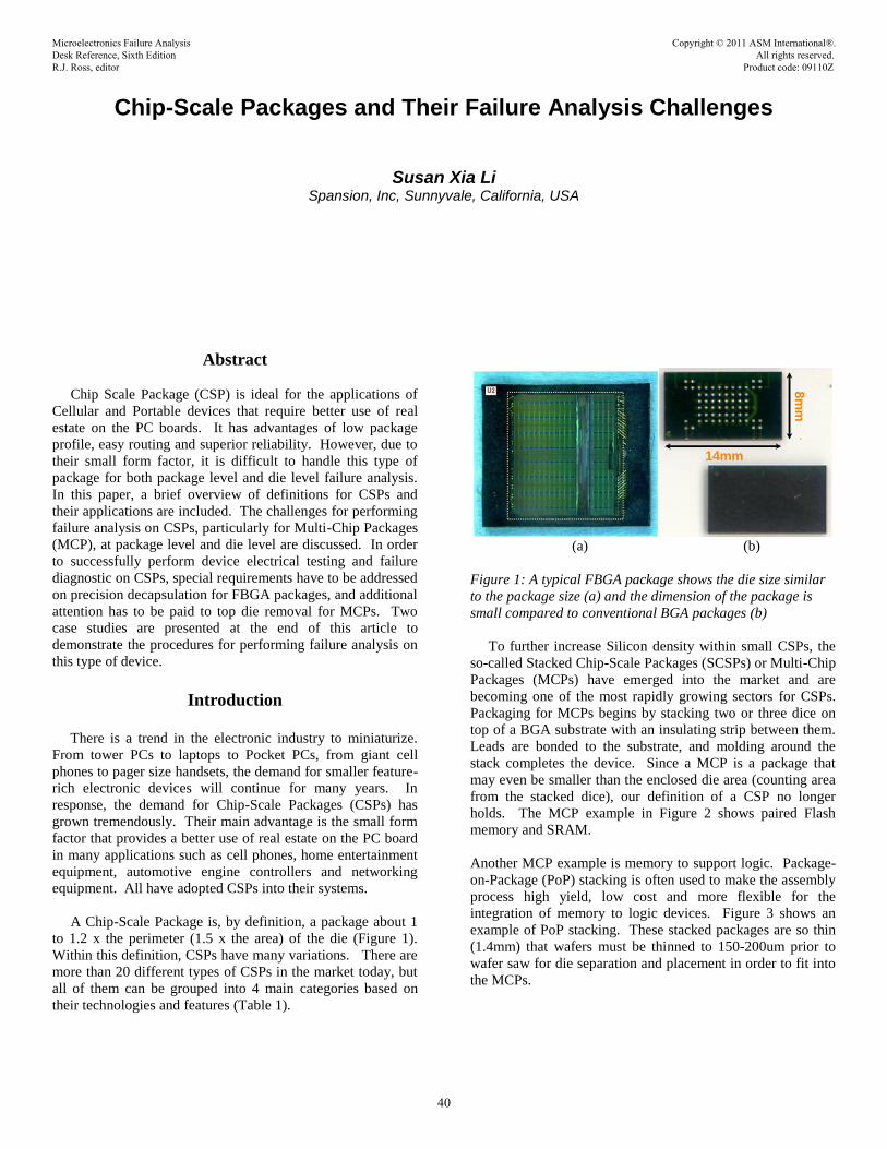
A Chip-Scale Package is, by definition, a package about 1
to 1.2 x the perimeter (1.5 x the area) of the die (Figure 1).
Within this definition, CSPs have many variations. There are
more than 20 different types of CSPs in the market today, but
all of them can be grouped into 4 main categories based on
their technologies and features (Table 1).
14mm
8m
m
(a) (b)
Figure 1: A typical FBGA package shows the die size similar
to the package size (a) and the dimension of the package is
small compared to conventional BGA packages (b)
To further increase Silicon density within small CSPs, the
so-called Stacked Chip-Scale Packages (SCSPs) or Multi-Chip
Packages (MCPs) have emerged into the market and are
becoming one of the most rapidly growing sectors for CSPs.
Packaging for MCPs begins by stacking two or three dice on
top of a BGA substrate with an insulating strip between them.
Leads are bonded to the substrate, and molding around the
stack completes the device. Since a MCP is a package that
may even be smaller than the enclosed die area (counting area
from the stacked dice), our definition of a CSP no longer
holds. The MCP example in Figure 2 shows paired Flash
memory and SRAM.
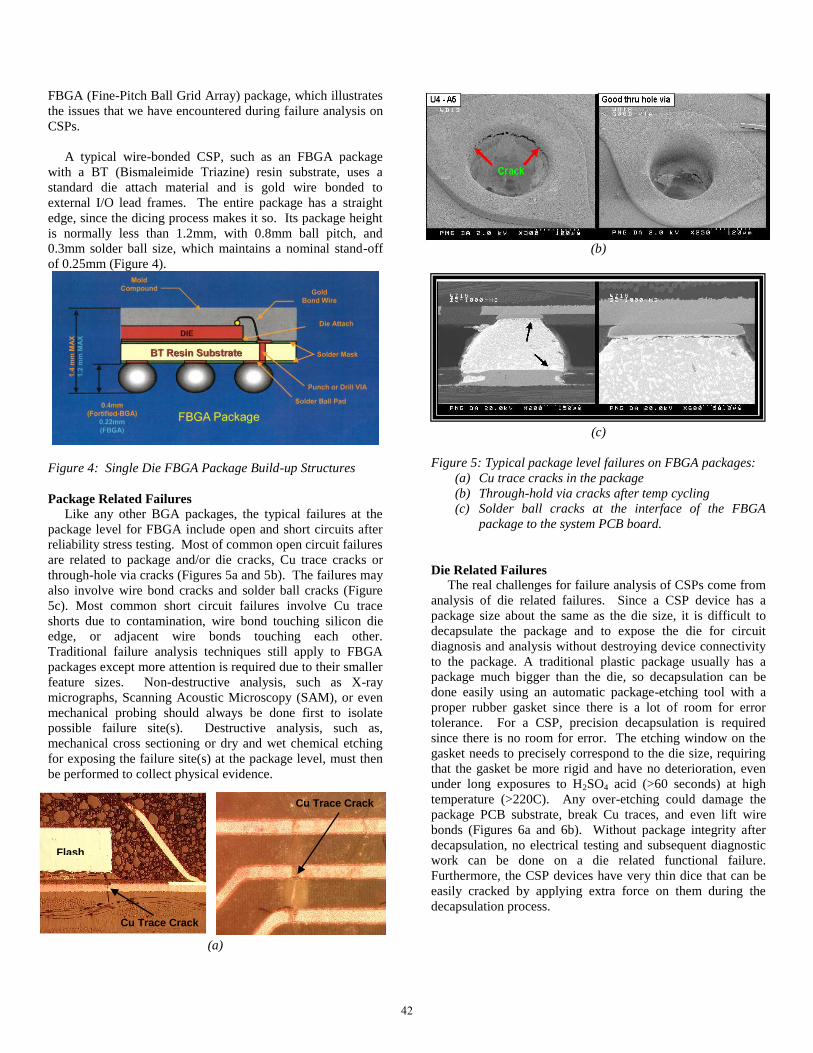
Another MCP example is memory to support logic. Package-
on-Package (PoP) stacking is often used to make the assembly
process high yield, low cost and more flexible for the
integration of memory to logic devices. Figure 3 shows an
example of PoP stacking. These stacked packages are so thin
(1.4mm) that wafers must be thinned to 150-200um prior to
wafer saw for die separation and placement in order to fit into
the MCPs.
Microelectronics Failure Analysis Desk Reference, Sixth Edition R.J. Ross, editor
Copyright © 2011 ASM International®. All rights reserved. Product code: 09110Z
40
Table 1: Four Main Categories for Chip Scale Packages
TECHNOLOGY REMARKS
Flexible Substrate It uses a flex circuit
interconnect as a substrate by
which the chip is connect to the
circuit board. There are two
ways of interconnecting the
chip to the substrate: flip chip
bonding and TAB style lead
bonding.
FBGA-PI
As for wire bond type, the chip
is protected using conventional
molding technology
Rigid Substrate
Organic Or Ceramic This type of CSPs has a ceramic
or an organic laminated rigid
substrate. Either conventional
wire bonding or flip chip can be
used to connect the die to the
substrate.
JACS-Pak
The wire bond version can be
considered as a downsized
version of the standard PBGA
even though assembly
techniques could be different.
Lead Frame Type The most common CSPs of this
type are the LOCs (Lead on
Chip) where the lead frame
extends over the top of the chip.
Wafer Scale This type of CSPs has the chips
that are processed in wafer form
before singulation. A re-
distribution layer is created in
the wafer scribe to pin out the
bond pads to a standard ball
grid array footprint.
(a)
(b)
Figure 2: A two die stacked MCP package with SRAM on top
of Flash configuration: (a) top view of the MCP package (b)
cross-sectional view of the MCP package
Figure3: PoP stacking provides high yield, low cost and more
flexible assembly process for the integration of memory to
logic devices
Failure Analysis Challenges
The many advantages that CSPs bring to the IC
applications also bring new challenges for device testing and
failure analysis at both the package and die levels. Since they
are small, device handling for CSP operations is difficult. The
following discussion mainly focuses on one type of CSPs, the
BBTT RReessiinn SSuubbssttrraattee
DIE 2
DIE 1
FBGA-BT
Micro BGA
LOC/SON
Ultra CSP
41
FBGA (Fine-Pitch Ball Grid Array) package, which illustrates
the issues that we have encountered during failure analysis on
CSPs.
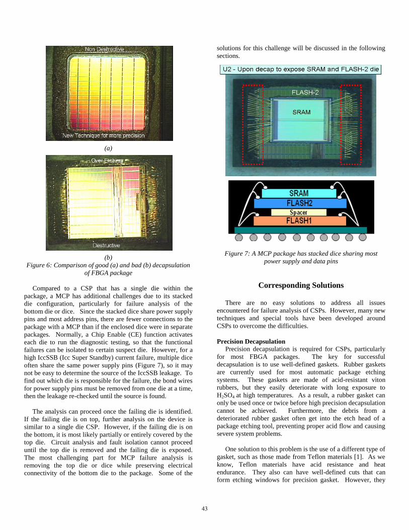
A typical wire-bonded CSP, such as an FBGA package
with a BT (Bismaleimide Triazine) resin substrate, uses a
standard die attach material and is gold wire bonded to
external I/O lead frames. The entire package has a straight
edge, since the dicing process makes it so. Its package height
is normally less than 1.2mm, with 0.8mm ball pitch, and
0.3mm solder ball size, which maintains a nominal stand-off
of 0.25mm (Figure 4).
Figure 4: Single Die FBGA Package Build-up Structures
Package Related Failures
Like any other BGA packages, the typical failures at the
package level for FBGA include open and short circuits after
reliability stress testing. Most of common open circuit failures
are related to package and/or die cracks, Cu trace cracks or
through-hole via cracks (Figures 5a and 5b). The failures may
also involve wire bond cracks and solder ball cracks (Figure
5c). Most common short circuit failures involve Cu trace
shorts due to contamination, wire bond touching silicon die
edge, or adjacent wire bonds touching each other.
Traditional failure analysis techniques still apply to FBGA
packages except more attention is required due to their smaller
feature sizes. Non-destructive analysis, such as X-ray
micrographs, Scanning Acoustic Microscopy (SAM), or even
mechanical probing should always be done first to isolate
possible failure site(s). Destructive analysis, such as,
mechanical cross sectioning or dry and wet chemical etching
for exposing the failure site(s) at the package level, must then
be performed to collect physical evidence.
(a)
(b)
(c)
Figure 5: Typical package level failures on FBGA packages:
(a) Cu trace cracks in the package
(b) Through-hold via cracks after temp cycling
(c) Solder ball cracks at the interface of the FBGA
package to the system PCB board.
Die Related Failures
The real challenges for failure analysis of CSPs come from
analysis of die related failures. Since a CSP device has a
package size about the same as the die size, it is difficult to
decapsulate the package and to expose the die for circuit
diagnosis and analysis without destroying device connectivity
to the package. A traditional plastic package usually has a
package much bigger than the die, so decapsulation can be
done easily using an automatic package-etching tool with a
proper rubber gasket since there is a lot of room for error
tolerance. For a CSP, precision decapsulation is required
since there is no room for error. The etching window on the
gasket needs to precisely correspond to the die size, requiring
that the gasket be more rigid and have no deterioration, even
under long exposures to H2SO4 acid (>60 seconds) at high
temperature (>220C). Any over-etching could damage the
package PCB substrate, break Cu traces, and even lift wire
bonds (Figures 6a and 6b). Without package integrity after
decapsulation, no electrical testing and subsequent diagnostic
work can be done on a die related functional failure.
Furthermore, the CSP devices have very thin dice that can be
easily cracked by applying extra force on them during the
decapsulation process.
Cu Trace Crack
Cu Trace Crack
Crack Flash Die
Cu Trace Crack
42
(a)
(b)
Figure 6: Comparison of good (a) and bad (b) decapsulation
of FBGA package
Compared to a CSP that has a single die within the
package, a MCP has additional challenges due to its stacked
die configuration, particularly for failure analysis of the
bottom die or dice. Since the stacked dice share power supply
pins and most address pins, there are fewer connections to the
package with a MCP than if the enclosed dice were in separate
packages. Normally, a Chip Enable (CE) function activates
each die to run the diagnostic testing, so that the functional
failures can be isolated to certain suspect die. However, for a
high IccSSB (Icc Super Standby) current failure, multiple dice
often share the same power supply pins (Figure 7), so it may
not be easy to determine the source of the IccSSB leakage. To
find out which die is responsible for the failure, the bond wires
for power supply pins must be removed from one die at a time,
then the leakage re-checked until the source is found.
The analysis can proceed once the failing die is identified.
If the failing die is on top, further analysis on the device is
similar to a single die CSP. However, if the failing die is on
the bottom, it is most likely partially or entirely covered by the
top die. Circuit analysis and fault isolation cannot proceed
until the top die is removed and the failing die is exposed.
The most challenging part for MCP failure analysis is
removing the top die or dice while preserving electrical
connectivity of the bottom die to the package. Some of the
solutions for this challenge will be discussed in the following
sections.
Figure 7: A MCP package has stacked dice sharing most
power supply and data pins
Corresponding Solutions
There are no easy solutions to address all issues
encountered for failure analysis of CSPs. However, many new
techniques and special tools have been developed around
CSPs to overcome the difficulties.
Precision Decapsulation
Precision decapsulation is required for CSPs, particularly
for most FBGA packages. The key for successful
decapsulation is to use well-defined gaskets. Rubber gaskets
are currently used for most automatic package etching
systems. These gaskets are made of acid-resistant viton
rubbers, but they easily deteriorate with long exposure to
H2SO4 at high temperatures. As a result, a rubber gasket can
only be used once or twice before high precision decapsulation
cannot be achieved. Furthermore, the debris from a
deteriorated rubber gasket often get into the etch head of a
package etching tool, preventing proper acid flow and causing
severe system problems.
One solution to this problem is the use of a different type of
gasket, such as those made from Teflon materials [1]. As we
know, Teflon materials have acid resistance and heat
endurance. They also can have well-defined cuts that can
form etching windows for precision gasket. However, they
43
may not have as much flexibility as rubber materials to
provide an airtight environment for the automatic package
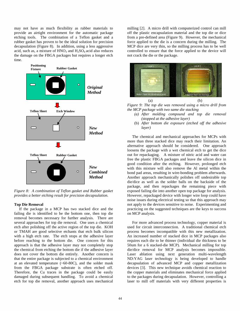
etching tools. The combination of a Teflon gasket and a
rubber gasket has proven to be the ideal solution for precision
decapsulation (Figure 8). In addition, using a less aggressive
acid, such as, a mixture of HNO3 and H2SO4 acid also reduces
the damage on the FBGA packages but requires a longer etch
time.
Figure 8: A combination of Teflon gasket and Rubber gasket
provides a better etching result for precision decapsulation.
Top Die Removal
If the package in a MCP has two stacked dice and the
failing die is identified to be the bottom one, then top die
removal becomes necessary for further analysis. There are
several approaches for top die removal. One uses a chemical
etch after polishing off the active region of the top die. KOH
or TMAH are good selective etchants that etch bulk silicon
with a high etch rate. The etch stops at the adhesive layer
before reaching to the bottom die. One concern for this
approach is that the adhesive layer may not completely stop
the chemical from etching the bottom die if the adhesive layer
does not cover the bottom die entirely. Another concern is
that the entire package is subjected to a chemical environment
at an elevated temperature (~60-80C), and the solder mask
from the FBGA package substrate is often etched off.
Therefore, the Cu traces in the package could be easily
damaged during subsequent handling. To avoid a chemical
etch for top die removal, another approach uses mechanical
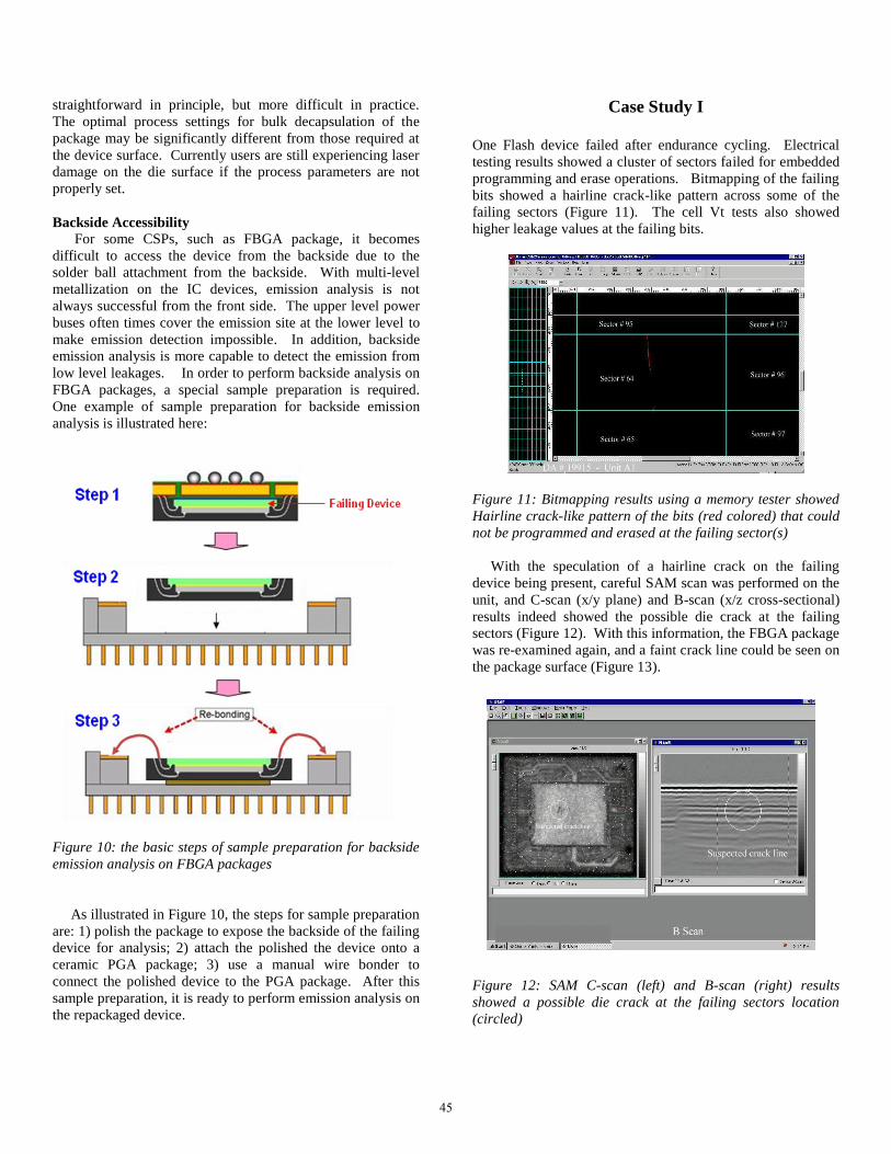
milling [2]. A micro drill with computerized control can mill
off the plastic encapsulation material and the top die or dice
from a pre-defined area (Figure 9). However, the mechanical
force applied to the die is a concern during the milling. The
MCP dice are very thin, so the milling process has to be well
controlled to ensure that the force applied to the device will
not crack the die or the package.
(a) (b)
Figure 9: The top die was removed using a micro drill from
the MCP package with two same die stacking
(a) After molding compound and top die removal
(stopped at the adhesive layer)
(b) After bottom die exposure (etched off the adhesive
layer)
The chemical and mechanical approaches for MCPs with
more than three stacked dice may reach their limitation. An
alternative approach should be considered. One approach
loosens the package with a wet chemical etch to get the dice
out for repackaging. A mixture of nitric acid and water can
free the plastic FBGA packages and leave the silicon dice in
good condition after the etching. However, prolonged etch
with this mixture will also remove the Al metal within the
bond pad areas, resulting in wire-bonding problem afterwards.
Another approach mechanically polishes off undesirable top
die/dice as well as the solder balls on the backside of the
package, and then repackages the remaining piece with
exposed failing die into another open top package for analysis.
However, repackaged device with longer wire loop could have
noise issues during electrical testing so that this approach may
not apply to the devices sensitive to noise. Experimenting and
practicing on the suggested techniques are the keys to success
on MCP analysis.
For more advanced process technology, copper material is
used for circuit interconnection. A traditional chemical etch
process becomes incompatible with this new metallization.
An increased number of stacked dice in MCP packages also
requires each die to be thinner (individual die thickness to be
50um for a 6 stacked-die MCP). Mechanical milling for top
die/dice removal for MCP analysis becomes impossible.
Laser ablation using next generation multi-wavelength
ND:YAG laser technology is being developed to handle
decapsulation of advanced MCP and copper metallization
devices [3]. This new technique avoids chemical reaction to
the copper materials and eliminates mechanical force applied
to the packages during decapsulation. However, controlling a
laser to mill off materials with very different properties is
Positioning
Fixture
Original
Method
New
Method
New
Combined
Method
Rubber Gasket
Teflon Sheet Etch Window
Teflon Sheet Rubber Gasket
44
straightforward in principle, but more difficult in practice.
The optimal process settings for bulk decapsulation of the
package may be significantly different from those required at
the device surface. Currently users are still experiencing laser
damage on the die surface if the process parameters are not
properly set.
Backside Accessibility
For some CSPs, such as FBGA package, it becomes
difficult to access the device from the backside due to the
solder ball attachment from the backside. With multi-level
metallization on the IC devices, emission analysis is not
always successful from the front side. The upper level power
buses often times cover the emission site at the lower level to
make emission detection impossible. In addition, backside
emission analysis is more capable to detect the emission from
low level leakages. In order to perform backside analysis on
FBGA packages, a special sample preparation is required.
One example of sample preparation for backside emission
analysis is illustrated here:
Figure 10: the basic steps of sample preparation for backside
emission analysis on FBGA packages
As illustrated in Figure 10, the steps for sample preparation
are: 1) polish the package to expose the backside of the failing
device for analysis; 2) attach the polished the device onto a
ceramic PGA package; 3) use a manual wire bonder to
connect the polished device to the PGA package. After this
sample preparation, it is ready to perform emission analysis on
the repackaged device.
Case Study I
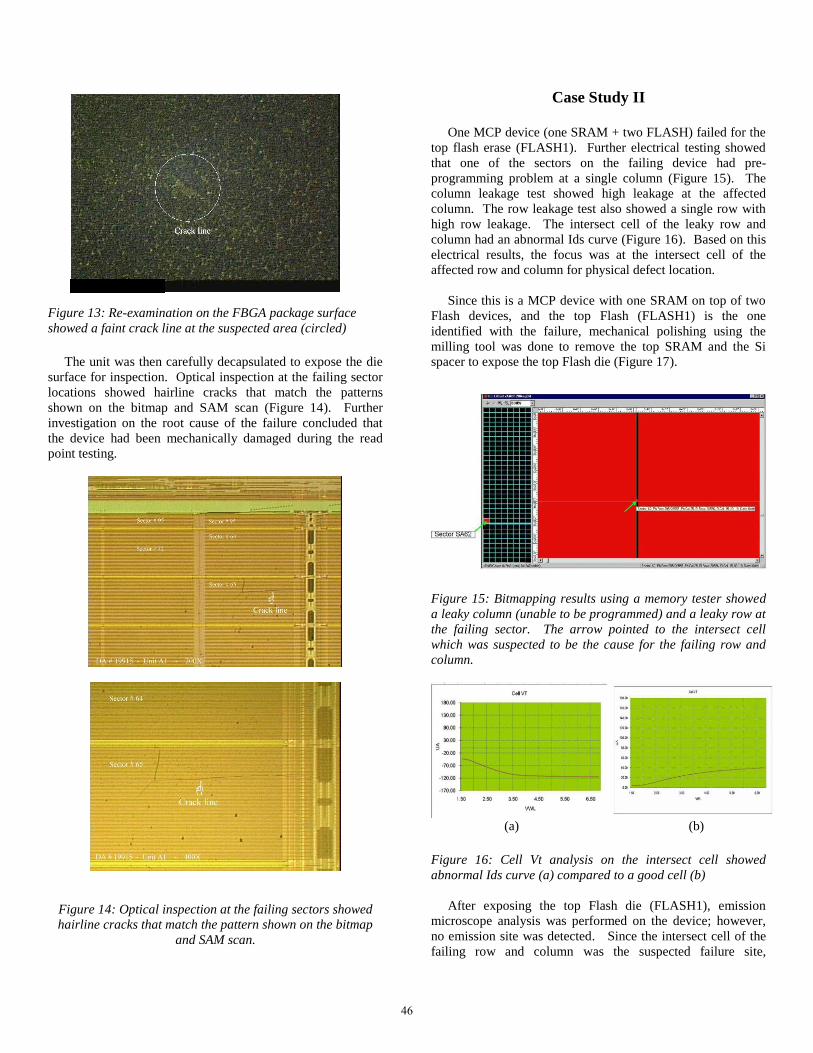
One Flash device failed after endurance cycling. Electrical
testing results showed a cluster of sectors failed for embedded
programming and erase operations. Bitmapping of the failing
bits showed a hairline crack-like pattern across some of the
failing sectors (Figure 11). The cell Vt tests also showed
higher leakage values at the failing bits.
Figure 11: Bitmapping results using a memory tester showed
Hairline crack-like pattern of the bits (red colored) that could
not be programmed and erased at the failing sector(s)
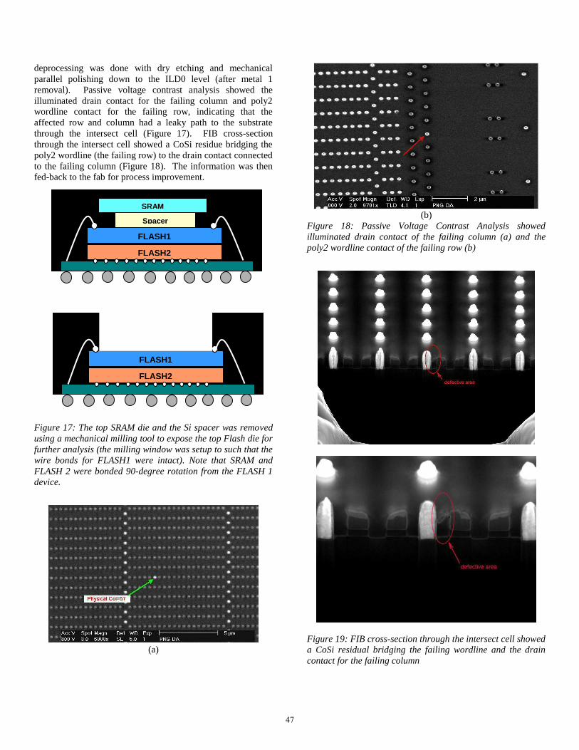
With the speculation of a hairline crack on the failing
device being present, careful SAM scan was performed on the
unit, and C-scan (x/y plane) and B-scan (x/z cross-sectional)
results indeed showed the possible die crack at the failing
sectors (Figure 12). With this information, the FBGA package
was re-examined again, and a faint crack line could be seen on
the package surface (Figure 13).
Figure 12: SAM C-scan (left) and B-scan (right) results
showed a possible die crack at the failing sectors location
(circled)
45
Figure 13: Re-examination on the FBGA package surface
showed a faint crack line at the suspected area (circled)
The unit was then carefully decapsulated to expose the die
surface for inspection. Optical inspection at the failing sector
locations showed hairline cracks that match the patterns
shown on the bitmap and SAM scan (Figure 14). Further
investigation on the root cause of the failure concluded that
the device had been mechanically damaged during the read
point testing.
Figure 14: Optical inspection at the failing sectors showed
hairline cracks that match the pattern shown on the bitmap
and SAM scan.
Case Study II
One MCP device (one SRAM + two FLASH) failed for the
top flash erase (FLASH1). Further electrical testing showed
that one of the sectors on the failing device had pre-
programming problem at a single column (Figure 15). The
column leakage test showed high leakage at the affected
column. The row leakage test also showed a single row with
high row leakage. The intersect cell of the leaky row and
column had an abnormal Ids curve (Figure 16). Based on this
electrical results, the focus was at the intersect cell of the
affected row and column for physical defect location.
Since this is a MCP device with one SRAM on top of two
Flash devices, and the top Flash (FLASH1) is the one
identified with the failure, mechanical polishing using the
milling tool was done to remove the top SRAM and the Si
spacer to expose the top Flash die (Figure 17).
Figure 15: Bitmapping results using a memory tester showed
a leaky column (unable to be programmed) and a leaky row at
the failing sector. The arrow pointed to the intersect cell
which was suspected to be the cause for the failing row and
column.
(a) (b)
Figure 16: Cell Vt analysis on the intersect cell showed
abnormal Ids curve (a) compared to a good cell (b)
After exposing the top Flash die (FLASH1), emission
microscope analysis was performed on the device; however,
no emission site was detected. Since the intersect cell of the
failing row and column was the suspected failure site,
46
deprocessing was done with dry etching and mechanical
parallel polishing down to the ILD0 level (after metal 1
removal). Passive voltage contrast analysis showed the
illuminated drain contact for the failing column and poly2
wordline contact for the failing row, indicating that the
affected row and column had a leaky path to the substrate
through the intersect cell (Figure 17). FIB cross-section
through the intersect cell showed a CoSi residue bridging the
poly2 wordline (the failing row) to the drain contact connected
to the failing column (Figure 18). The information was then
fed-back to the fab for process improvement.
Figure 17: The top SRAM die and the Si spacer was removed
using a mechanical milling tool to expose the top Flash die for
further analysis (the milling window was setup to such that the
wire bonds for FLASH1 were intact). Note that SRAM and
FLASH 2 were bonded 90-degree rotation from the FLASH 1
device.
(a)
(b)
Figure 18: Passive Voltage Contrast Analysis showed
illuminated drain contact of the failing column (a) and the
poly2 wordline contact of the failing row (b)
Figure 19: FIB cross-section through the intersect cell showed
a CoSi residual bridging the failing wordline and the drain
contact for the failing column
FLASH2
FLASH1 Spacer
SRAM
FLASH2
FLASH1
Spacer
SRAM
47
Summary
CSPs are getting increasingly more attention due to their
advantages of small form factor, cost effectiveness and PCB
optimization. They are widely utilized for hand-held devices,
automotive engine controller and networking equipment.
Their small size creates new challenges for testing and failure
analysis. Special requirements, such as precision
decapsulation for FBGA packages, top die removal for MCP
packages, must be addressed in order to successfully perform
device testing and diagnostic analysis. In this article, some
new challenges and corresponding solutions were discussed to
increase the awareness of particular issues associated with
CSPs. Two case studies are used to demonstrate how a typical
CSP failure analysis is done.
References [1] Xia Li, Joseph Vu, Mohammad Massoodi and Jose Hulog,
“Automatic decapsulation system utilizing an acid resistant,
high heat endurance and flexible sheet coupled to a rubber
gasket and a method of us”, US Patent Number 6409878
(2002)
[2] Ultratec Application Note, “Enabling Backside Analysis,
an overview of Selected Area Preparation”, 2002
[3] Control Systemation, Inc, Application Note by Jon W.
Heyl, “Laser Based Failure Analysis, including Decapsulation,
Cross-sectioning and Materials Characterization”, 2004
Acknowledgements
The author would like to acknowledge following people for
their contributions to this publication:
Joseph Vu and Shamsual Mohamed for their device
anlaysis data
Jose Hulog, Mohammad Massodi and Joseph Vu for co-
developping the precision decapsulation technique
Mario Vargas for providing precision decapsulation
images
Gene Daszko and Andy Gray for reviewing this paper and
providing valuable input
48