Page 1
MIDSWEDEN UNIVERSITY
Assessment and Development of
Advanced Power Saving and Supply
Concepts
For Small Automotive Electronics
by
Muhammed Mustafa TARHAN
A thesis submitted in partial fulfillment for the
Master Degree in Electronic Design
in the
INFORMATION TECHNOLOGY AND MEDIA
MSc in Electronic Design
January 2013
Page 2
Declaration of Authorship
I, Muhammed Mustafa TARHAN, declare that this thesis titled, ‘Assessment and De-
velopment of Advanced Power Saving and Supply Concepts For Small Automotive Elec-
tronics’ and the work presented in it are my own. I confirm that:
This work was done wholly or mainly while in candidature for a research degree
at this University.
Where any part of this thesis has previously been submitted for a degree or any
other qualification at this University or any other institution, this has been clearly
stated.
Where I have consulted the published work of others, this is always clearly at-
tributed.
Where I have quoted from the work of others, the source is always given. With
the exception of such quotations, this thesis is entirely my own work.
I have acknowledged all main sources of help.
Where the thesis is based on work done by myself jointly with others, I have made
clear exactly what was done by others and what I have contributed myself.
Signed:
Date:
i
Page 3
”As we express our gratitude, we must never forget that the highest appreciation is not
to utter words, but to live by them. ”
John F. Kennedy
Page 4
MIDSWEDEN UNIVERSITY
Abstract
INFORMATION TECHNOLOGY AND MEDIA
MSc in Electronic Design
MSc in Electroncs
by Muhammed Mustafa TARHAN
With rising fuel prices, increasing electrification, and imminent fines on CO2 emission
within the EU, the requirement for energy and cost efficient supply concepts is becoming
more and more important in the automotive industry. This thesis presents an assessment
of, and improvement for energy and cost efficient power supply concepts for low-end au-
tomotive and light e-mobility electronic control units, containing small µCs, and analog
and logic components.
Specifically, linear regulators, synchronous and non-synchronous buck converters, and
switched capacitor converters are investigated and assessed theoretically. The most
promising concept, namely a discrete buck converter, is further studied using theoretical
assessment, experiment, and simulations.
The key result of this work is a concept for replacing commonly used linear regulators
in small electronic control units (ECUs) by a more efficient supply with only a small
cost adder. Specifically, since no low-end switched converter ICs are available today, we
developed a buck converter with discrete control circuit. This concept provides a cheap,
yet efficient alternative to linear regulators for a wide range of applications. In addition,
the application of this concept is supported by component selection criteria, and also by
the developed simulation models.
Page 5
Acknowledgements
First of all I owe my gratitude to Dr. Georg Icking-Konert for his continued encour-
agement, guidance and technical advise, and for offering the opportunity to work for
the Robert Bosch GmbH. This thesis would not have been possible without his support,
both professionally and personally.
I also want to take this opportunity to express my profound gratitude and deep regards to
my mentor Prof. Bengt Oelmann for his exemplary guidance, monitoring and constant
encouragement before and after this thesis. The support and guidance given by him
time and again shall carry me a long way on the journey of life, on which I am about to
embark.
I am indebted to all my colleagues at the university department for providing a great
working environment. I also would like to express my gratitude to the teams from Robert
Bosch GmbH, Dialog Semiconductor AG, and Infineon Technologies AG, for many good
discussions and their profound and competent technical support.
I wish to thank my friends Zeynep Islam, Mehmet Gulay, Hakan Gulay, Yunus Tarhan,
Cem Kultepe, Kaan Girgic, Aart Mulder, Veysel Bali, Said Nur Yilmaz, Mahmud Se-
lim, Cem Demir, Mustafa Ozan Capa, Alper Coban, Sarah Metzker Erdemir, Prof. Paul
Yule, Zakarya Bamohamed, Muhammad Imran Khan, Muhammad Amir, Ahmed Khan,
Merve Oral, Cagri Demirtas, Emile Wattsohn, Ralf Gartig, Rabia Dogan, Bruno Jun-
queira, Nils Holler, Paresh Paresh Mestri, Juliana Berzina, and Anastasia Aladeva for
helping me get through difficult times.
As Jane Howard says, ”Call it a clan, call it a network, call it a tribe, call it a family.
Whatever you call it, whoever you are, you need one”. And I was needing their support
during this thesis process, which is why I feel indebted to thank my father Fecri Tarhan
and my mother Ayten Tarhan, my lovely sisters, Emine Sarac, Sabire Tarhan Gulay,
Gulbin Tarhan and Nida Tarhan, and also my brothers-in-law Nazim Sarac and Ayhan
Gulay. And, last but not least, I want to thank my nephew Burak and my niece Berra
Sarac for their support throughout my research process.
iv
Page 6
Contents
Declaration of Authorship i
Abstract iii
Acknowledgements iv
List of Figures vii
List of Tables ix
Abbreviations x
Symbols xi
1 Introduction 1
1.1 Motivation . . . . . . . . . . . . . . . . . . . . . . . . . . . . . . . . . . . 1
1.2 Today’s Solution in Automotive . . . . . . . . . . . . . . . . . . . . . . . . 4
1.3 State of Art in Mobile Electronics . . . . . . . . . . . . . . . . . . . . . . 5
1.4 Research Problem . . . . . . . . . . . . . . . . . . . . . . . . . . . . . . . 6
1.4.1 Open Points . . . . . . . . . . . . . . . . . . . . . . . . . . . . . . . 6
1.5 Commitment . . . . . . . . . . . . . . . . . . . . . . . . . . . . . . . . . . 7
2 Requirements 8
2.1 Requirements in Automotive and light e-mobility . . . . . . . . . . . . . . 8
2.2 Scope of the Work . . . . . . . . . . . . . . . . . . . . . . . . . . . . . . . 10
3 Theory 11
3.1 Linear Regulator . . . . . . . . . . . . . . . . . . . . . . . . . . . . . . . . 13
3.2 Buck Converter . . . . . . . . . . . . . . . . . . . . . . . . . . . . . . . . . 16
3.2.1 Non-Synchronous Buck Converter . . . . . . . . . . . . . . . . . . 17
3.2.2 Synchronous Buck Converter . . . . . . . . . . . . . . . . . . . . . 22
3.3 Switched Capacitor Converter . . . . . . . . . . . . . . . . . . . . . . . . . 24
3.4 Closed Loop Control and Compensation Technique . . . . . . . . . . . . . 28
3.4.1 Type 1 Control . . . . . . . . . . . . . . . . . . . . . . . . . . . . . 29
3.4.2 Type 2 Control . . . . . . . . . . . . . . . . . . . . . . . . . . . . . 30
v
Page 7
Contents vi
3.4.3 Type 3 Control Method . . . . . . . . . . . . . . . . . . . . . . . . 32
3.4.4 Feedback Control . . . . . . . . . . . . . . . . . . . . . . . . . . . . 34
4 Concept and Implementation 36
4.1 Component Selection for Buck Converter . . . . . . . . . . . . . . . . . . 36
4.1.1 Inductor Selection . . . . . . . . . . . . . . . . . . . . . . . . . . . 36
4.1.2 MOSFET Selection . . . . . . . . . . . . . . . . . . . . . . . . . . . 38
4.1.3 Output Capacitor Selection . . . . . . . . . . . . . . . . . . . . . . 42
4.1.4 Free Wheeling Diode Selection . . . . . . . . . . . . . . . . . . . . 44
4.2 Switching Frequency Selection for Buck Converter . . . . . . . . . . . . . 45
4.3 Compensation Network for Buck Converter . . . . . . . . . . . . . . . . . 46
5 Methods 49
5.1 Experimental Validation . . . . . . . . . . . . . . . . . . . . . . . . . . . . 49
5.2 Simulation Models . . . . . . . . . . . . . . . . . . . . . . . . . . . . . . . 52
6 Results and Discussion 55
6.1 Experimental Validation . . . . . . . . . . . . . . . . . . . . . . . . . . . . 55
6.2 Non Synchronous Buck Converter Simulation Results . . . . . . . . . . . . 59
6.3 Synchronous Buck Converter Simulation Results . . . . . . . . . . . . . . 64
6.4 Small Signal Analysis . . . . . . . . . . . . . . . . . . . . . . . . . . . . . 65
7 Conclusion 68
8 Advanced Energy Saving Concepts 69
8.1 Deactivating Unused Hardware . . . . . . . . . . . . . . . . . . . . . . . . 70
8.2 Dynamic Clock Scaling . . . . . . . . . . . . . . . . . . . . . . . . . . . . . 70
8.2.1 Timing of Frequency Change . . . . . . . . . . . . . . . . . . . . . 71
8.2.2 Automatic Load Determination . . . . . . . . . . . . . . . . . . . . 74
9 Summary and Outlook 76
9.1 Summary . . . . . . . . . . . . . . . . . . . . . . . . . . . . . . . . . . . . 76
9.2 Limitations . . . . . . . . . . . . . . . . . . . . . . . . . . . . . . . . . . . 76
9.3 Future Work . . . . . . . . . . . . . . . . . . . . . . . . . . . . . . . . . . 77
Bibliography 78
Page 8
List of Figures
1.1 Past and Targeted CO2 Emissions in the EU . . . . . . . . . . . . . . . . 2
1.2 CO2 emission targets for USA, China, and EU . . . . . . . . . . . . . . . 2
2.1 DC/DC Converter Block Diagram . . . . . . . . . . . . . . . . . . . . . . 9
3.1 Cascaded Linear Converters in Bosch e-Scooter Gen.1 . . . . . . . . . . . 14
3.2 Schematic of a non-synchronous buck converter . . . . . . . . . . . . . . . 16
3.3 Inductor current for continuous (left) and discontinuous mode (right) . . 16
3.4 Non-Synchronous Buck Converter: ON State . . . . . . . . . . . . . . . . 17
3.5 Non-Synchronous Buck Converter: OFF State . . . . . . . . . . . . . . . 17
3.6 Buck Converter Schematic with Internal Capacitor and internal InductorResistance . . . . . . . . . . . . . . . . . . . . . . . . . . . . . . . . . . . . 20
3.7 Buck Converter Typical Wave Form [14] . . . . . . . . . . . . . . . . . . . 20
3.8 Schematic of a synchronous buck converter . . . . . . . . . . . . . . . . . 22
3.9 Timing of MOSFET switching for Q1 (PWM1H) and Q2 (PWM1L) fora synchronous buck converter . . . . . . . . . . . . . . . . . . . . . . . . . 23
3.10 Basic Switched Capacitor Structure . . . . . . . . . . . . . . . . . . . . . . 24
3.11 Switched capacitor IC by V. Ng and S. Sanders [19] [20] . . . . . . . . . . 26
3.12 A simple Buck Converter Control Algorithm . . . . . . . . . . . . . . . . 28
3.13 Type 1 Control Schematic . . . . . . . . . . . . . . . . . . . . . . . . . . . 29
3.14 Type 1 Bode Plot for phase shift and gain margin . . . . . . . . . . . . . . 30
3.15 Type 2 Control Schematic . . . . . . . . . . . . . . . . . . . . . . . . . . . 30
3.16 Type 2 Bode Plot for phase shift and gain margin . . . . . . . . . . . . . . 31
3.17 Type 3 Control Schematic . . . . . . . . . . . . . . . . . . . . . . . . . . . 32
3.18 Type 3 Bode Plot for phase shift and gain margin . . . . . . . . . . . . . . 32
3.19 Current mode control circuit [24] . . . . . . . . . . . . . . . . . . . . . . . 34
4.1 Buck converter representation during ON time . . . . . . . . . . . . . . . 37
4.2 Inductor voltages and current during ON and OFF time . . . . . . . . . . 37
4.3 MOSFET structure with Drain (D), Gate (G), Source (S) and Body (B)[26] . . . . . . . . . . . . . . . . . . . . . . . . . . . . . . . . . . . . . . . . 39
4.4 Equivalent Circuit of PMOS Device . . . . . . . . . . . . . . . . . . . . . 40
4.5 Capacitor Charge and Discharge waveform . . . . . . . . . . . . . . . . . . 43
5.1 Simulation Model of Validation Circuit . . . . . . . . . . . . . . . . . . . . 51
5.2 Hardware Set-Up of Validation Circuit . . . . . . . . . . . . . . . . . . . . 51
5.3 Non-Synchronous Buck Converter Schematic with Compensation Network 53
5.4 Synchronous Buck Converter Schematic with Compensation Network . . . 54
vii
Page 9
List of Figures viii
6.1 PWM Voltage of Experimental and Simulated Circuit . . . . . . . . . . . . 56
6.2 Gate Voltage of Experimental and Simulated Circuit . . . . . . . . . . . . 56
6.3 Drain Voltage of Experimental and Simulated Circuit . . . . . . . . . . . . 57
6.4 Output voltage comparison of experimental and simulated circuit . . . . . 57
6.5 waveforms for the experimental set up . . . . . . . . . . . . . . . . . . . 58
6.6 waveform for the simulation set up . . . . . . . . . . . . . . . . . . . . . . 58
6.7 Output Voltage Overshoot (left), and Effect of Start Up Circuit (right) . . 59
6.8 Output Voltage Ripple of Non-Synchronous Buck Converter . . . . . . . . 60
6.9 Improved Output Ripple of Non-Synchronous Buck Converter . . . . . . . 60
6.10 Transient Currents and Voltages in the Non-Synchronous Buck Converter 61
6.11 EMC Model of the Power Supply . . . . . . . . . . . . . . . . . . . . . . . 62
6.12 EMC Line Emission of Non-Synchronous Buck Converter . . . . . . . . . 62
6.13 Power Efficiency of Non-Synchronous Buck Converter . . . . . . . . . . . 63
6.14 Power Efficiency of Synchronous Buck Converter . . . . . . . . . . . . . . 64
6.15 Small Signal Analysis of the Buck Converter . . . . . . . . . . . . . . . . 65
6.16 Bode Plot of the Compensation Network and Output Voltage . . . . . . . . 66
6.17 Power Stage LC Circuit Bode Plot . . . . . . . . . . . . . . . . . . . . . . 67
Page 10
List of Tables
1.1 Emission of CO2 per gasoline consumption . . . . . . . . . . . . . . . . . 2
2.1 Requirements for DC/DC Converters . . . . . . . . . . . . . . . . . . . . . 10
4.1 Components for Compensation and Power Stage . . . . . . . . . . . . . . 48
ix
Page 11
Abbreviations
ACEA European Automotive Manufacturers Association
BJT Bipolar Junction Transistor
CAN Controller Area Network
CMC Current Mode Control
CMOS Complementary Metal Oxide Semiconductor
ECU Electronic Control Unit
EMC Electro Magnetic Compatibility
EME Electro Magnetic Emission
EMI Electro Magnetic Interference
ESR Equivalent Serial Resistance
ESL Equivalent Serial Inductance
GM Gain Margin
JAMA Japan Automobile Manufacturers Association
KAMA Korea Automobile Manufacturers Association
LIR Load Current Ripple
LIN Local Interconnect Network
MOSFET Metal Oxide Semiconductor Field Effect Transistor
PCB Printed Circuit Board
PM Phase Margin
SC Switched Capacitor
SLI Starting Lighting Ignition
SPICE Simulation Program with Integrated Circuit Emphasis
VDA Verband der Automobilindustrie (German Automotive Manufacturers Association)
VMC Voltage Mode Control
µC MicroController (with embedded memory and peripherals)
x
Page 12
Symbols
P power W (Js−1)
rDSON MOSFET ON Resistance Ohm
Vin input Voltage Volt
Vout output Voltage Volt
ILOAD Load Current Ampere
Cout Output Capacitance Farad
L Inductance Henry
η Efficiency %
xi
Page 13
Dedicated to my loving father and mother.... . .
xii
Page 14
Chapter 1
Introduction
1.1 Motivation
The importance of global climate protection is universally acknowledged, due to its
impact on the environment, and thus also mankind. Consequently much effort is being
put into reducing the emission of greenhouse gases, both by governments and non-
governmental organizations around the world.
According to recent research results [1], transport related energy consumption already
accounts for approximately 20% of the world’s total energy consumption. And this
number is still growing, due to the ever increasing number of cars per capita. And since
the vast majority of cars is still powered by fossil fuel, this results in a large and yet
growing CO2 emission.
To counter this trend, in 1995 the German Association of the Automotive Industry
(Verband der Automobilindustrie, VDA, [2]) committed itself to reduce the average
CO2 emission of new cars by 25% between 1990 and 2005. According to the European
Automotive Manufacturers’ Association (ACEA, [3]) this goal was almost achieved [4].
Three years later, the ACEA committed itself to decrease the average CO2 emission
to 140g/km by 2008. Similar announcements were made by the associated Japanese
(JAMA, [5]) and Korean (KAMA, [6]) car manufacturers one year later.
On governmental side the European Union Energy Commission has recently passed
a regulation to gradually reduce CO2 emissions to 95g/km in 2020, from an average
emission of 135.7g/km in 2011 [7], see figure 1.1. According to this regulation, exceeding
the limit for the average emission of a manufacturer’s fleet will be fined. The penalty
is gradually increasing over time, reaching e95 for every g/km above the legal limit in
2020.
1
Page 15
Chapter 1. Introduction 2
Figure 1.1: Past and Targeted CO2 Emissions in the EU
Similar regulations are also planned or already passed in other markets. For example,
USA and China have already announced plans to steadily reduce fuel consumption of
passenger cars, and thus CO2 emission (see figure 1.2).
Figure 1.2: CO2 emission targets for USA, China, and EU
The amount of CO2 emission of a car per distance is readily calculated from its fuel
consumption, since the amount of carbon per unit of fuel is given, and CO2 is one of the
inevitable products of the combustion reaction. For standard gasoline, the conversion is
shown in table 1.1, with colors indicating annual EU emission limits for 2008 (yellow),
2012 (red), and 2020 (blue), respectively.
l/100km 6,72 6,08 5,65 5.21 4,78 4,34 4,13
mpg 35,89 38,69 41,66 45,13 49,24 54,1 57,01
CO2/km 155 140 130 120 110 100 95
Table 1.1: Emission of CO2 per gasoline consumption
According to the above mentioned EU regulation, each saved gram CO2 will be worth
up to e95/car in the future. Or, vice versa, car manufacturers violating the legal limit
will be fined, with the absolute sums possibly reaching staggering numbers. Assume, for
example, a fleet of typical 2012 cars in with a CO2 emission of 130 gCO2/km (see fig. 1.1).
With the new EU regulation, in 2020 each car would be fined with approximately e3300
on average. In addition, rising fuel prices and customer awareness generate pressure
to further reduce fuel consumption. As a consequence there is a huge incentive for the
industry to develop ever more fuel-efficient combustion motors, and also energy efficient
electrical and electronic components.
Page 16
Chapter 1. Introduction 3
On the 13th International Conference on Electronics in Automotive [8], A.Graf and
B.Koppl, both Infineon Technologies AG, pointed out this challenge for the automo-
tive industry, and also proposed several methods of saving energy, e.g. by replacing
incandescent lighting by LEDs, more efficient actuators, or by so-called demand based
control of systems. They calculate the monetary value of each saved gram CO2/km, cor-
responding to 40W of electrical power, to e49.80/car. Notably the CO2 fine assumed
by the authors at the time was underestimated by a factor of three, compared to the
final EU regulation. Using the actual numbers, this value increases to e115/(gCO2×car), corresponding to e2.88/(W×car).
Independently, the corporate research group of Robert Bosch GmbH in November 2011
assessed the effect of the EU CO2 regulation for car manufacturers [9]. Assuming an
overall efficiency of 23.3% for the combustion motor, generator, and supply network,
they calculated the monetary value of each gram CO2/km to e3.142/(W×car). This
value is in good agreement with the above number by A.Graf and B.Koppl. According
to both reports, this will add significant pressure on the OEMs (and consequently on
the suppliers) to save power, even on the scale of small µC. As an example, assume a
13.5V battery voltage, and a small ECU consuming 25mA, e.g. a small sensor. This
corresponds to a power consumption of 337.5mW, and thus to a fine of ∼1 e/car.
Another industry with even higher incentives for energy efficiency is the mobile market.
There the overall trend is towards ever increasing performance and functionality, but
at constant or decreasing average power consumption. In comparison, automotive elec-
tronics is far behind with respect to electronics efficiency. Therefore, this thesis will also
assess energy saving techniques common in mobile electronics, and their applicability to
automotive and e-mobility applications.
Page 17
Chapter 1. Introduction 4
1.2 Today’s Solution in Automotive
The drive system of an automobile generally consists of an internal combustion engine,
axle, gear, and tires. Control and diagnostics of this systems is performed by a multitude
of electronic systems. In addition, many safety or comfort features today require elec-
tronic control units, e.g. ABS, ESP, power-steering, cooler fans, wipers, window lifters,
etc.. Today most ECUs are connected via busses, e.g. via Controller Area Network
(CAN) or Local Interconnect Network (LIN). As a consequence the complexity of car
electronics increases steadily, which in turn leads to an increase in its power consump-
tion.
Besides a very wide range of input voltages and ambient temperatures, the automotive
market is characterized by very high expectations regarding product lifetime, and a
very competitive market, especially for small commodity electronics. For these ECUs,
typically consuming<50mA, high cost pressure, tight space requirements, and the lack of
incentive for power efficient designs, have led to the wide-spread use of linear regulators.
These are easy to use, cheap, and small, but have a low conversion efficiency.
More efficient, but also more expensive and bulky, switched power supplies are gener-
ally restricted to high-end ECUs, typically using multi-core, 32-bit µCs and currents
>500mA. Other power-saving techniques, like adapting the core frequency and/or -
voltage, are rarely used in automotive electronics. Generally the risk of and effort for
dynamic frequency scaling in the past was assessed higher than the benefit of saving en-
ergy. As a consequence µCs generally always run at the speed, which is required under
highest load condition.
Since none of the commonly used automotive communication busses provide means to
selectively wake ECUs, several proposals have been made, which all focus on retaining
network topology and -communication, while allowing functions to be switched off to
save power. The most well-known ones are Partial Networking, Pretended Networking
and ECU Degradation:
• Partial Networking describes a group of ECUs, which are known as Partial
Network Clusters (PNC), which can be individually shut down or re-started, while
normal bus communication is ongoing. Basically, ECUs in the PNC cluster are
selectively put to sleep and woken, based on network identifier and user data. Cur-
rently, this concept is only specified for the CAN bus. The required ”intelligent”
transceivers, and the supporting software (SW) architectures are currently under
development [10].
Page 18
Chapter 1. Introduction 5
• Pretended Networking describes a network cluster, in which each ECU node
can independently decide if and when to enter power saving mode. Wake-up is
triggered by the respective bus wake event. If the time to resume communication
is sufficiently short, pretended networking has no impact on the communication or
other network nodes. Therefore it is very easy to integrate into existing networks.
Also it allows using standard transceivers, and requires only minor SW changes in
the affected ECU. However, the power saving potential is relatively small.
• ECU Degradation describes the temporary de-activation of unused components
inside an ECU. For example, a sensor required for BLDC motor commutation
can possibly be switched off, when the motor is not powered. ECU degradation
generally has no impact on network topology or -management, and is therefore easy
to integrate into existing cars. However, since it is highly application dependent,
it cannot be generalized like partial networking, and requires a careful assessment
of unwanted side-effects.
1.3 State of Art in Mobile Electronics
In contrast to the automotive market with its ”infinite” energy supply, mobile applica-
tions always had to put huge emphasis on making best use of the very restricted energy
capacitance of pocket-size batteries. As a consequence very advanced energy saving
strategies are commonly being used, like efficient supplies, load dependent clock scaling,
dynamic core voltage, switching off unused modules and cores, to name but a few.
The extremely high volumes in the mobile market, in combination with a high cost
pressure, have brought down prices of components significantly, e.g. for small inductors or
control-ICs for switched regulators. While these are generally not automotive qualified,
we will assess if, which, and for what applications these components might still be
used. Also we will assess which of the advanced software strategies could be adopted
in automotive electronics today, and which would require new hardware (HW) features,
currently not available in automotive components.
Page 19
Chapter 1. Introduction 6
1.4 Research Problem
As shown in section 1.1, there is a huge incentive for increasing energy efficiency also
in automotive electronics. At the same time, high cost pressure and tight space re-
quirements result in off-the-shelf switched DC/DC converters being too expensive for
ubiquitous low-end ECUs. As a recent, internal assessment by G.Icking-Konert showed,
a switched supply for a high-end µC, including printed circuit board (PCB) space etc.,
today adds ∼e4.50 to the product cost. This generally is acceptable for high-end (i.e. ex-
pensive) ECUs, but is in conflict with low-end ECU prices of only a few e/PCB.
Thus there is a high demand for a cost- end energy-efficient power supply concept, which
is targeted at small ECUs, typically consuming <50mA. This thesis focusses on assessing
several efficient and cost-effective DC/DC converter concepts for these low-end ECUs.
1.4.1 Open Points
At the start of this project, we need to have an understanding of the technical require-
ments in the targeted applications, and a roadmap to aid the design phase. The below
questions are the base to identify the technical requirements, and will be answered in
the next chapters.
• How much can power efficiency be increased, starting from a linear converter?
• Are there new, revolutionary DC/DC converter concepts, that are suited for au-
tomotive applications?
• What are the limits for the different converter types? Do these fit the require-
ments?
• Is this possible to design a sufficiently cost-effective switched DC/DC converter
for low-end ECUs? As a cost metrics, we assume achieved the CO2 fine reduction
vs. implementation cost
Page 20
Chapter 1. Introduction 7
1.5 Commitment
The result of this thesis will be a list of concepts for DC/DC converters suitable for
automotive and light e-mobility electronics. This list contains a theoretical assessment
of each concept, and its applicability for the targeted applications. In addition, we will
give a comparison of the technical requirements with the actual properties of each supply
concept. For the most promising concept, namely a non-synchronous buck converter, we
will propose a physical implementation, design rules for selecting components and control
parameters, and a validated simulation model for application specific optimization.
In detail, the above deliverables are committed as:
• this thesis focuses on small automotive ECUs and light e-mobility applications.
Therefore, we limit ourselves to automotive and light e-mobility applications with
a supply voltage range of 12V..60V, and logic supply currents of ∼25mA, e.g. e-
scooter. The result is a list of suitable supply concepts, together with a theoretical
and commercial comparison of all concepts. For one selected concept, also design
guidelines, known limits, and a SPICE [11] simulation model are provided.
• assessment of SW-strategies to decrease power consumption already in today’s
low-end µC, e.g. STM8 or S12G. The result is a SW concept with common fea-
tures (scheduler, timers, communication,...), and options for load dependent core
frequency. Here the focus is on measuring core load, and avoiding issues during
changes of core frequency or module state.
• assessment of further, more advanced power-saving features for future ICs. This
is targeted for a technical discussion with IC suppliers.
Page 21
Chapter 2
Requirements
In this chapter, we define the technical requirements for a DC/DC converter suitable for
the projects within the scope of this thesis, namely small automotive and light e-mobility
ECUs. There are several options for the logic supply of these electronics, which will be
discussed in detail below. By far the most common for small automotive electronics is
the ”linear converter”, due to it’s simplicity and price advantage (but low efficiency). To
assess alternative concepts, we first need to define the respective technical criteria. This
will be done in subsection ”Requirements in Automotive”. Afterward, we will assess all
investigated supply concepts with regard to these requirements.
2.1 Requirements in Automotive and light e-mobility
Typically, automotive power supply is based on a Vbat = 13.5V SLI (starting, lighting,
ignition) battery, which is recharged by a generator, mechanically coupled to a combus-
tion motor. However, the automotive voltage range is typically specified as 9..18V, with
transient voltages reaching 40V. All connected ECUs have to stand these voltages, thus
the supply for 3.3V or 5V µCs and sensors needs to be regulated down to the respective
working voltage.
In contrast, light e-mobility ECUs, e.g. for e-scooters, generally have battery voltages
higher than 12V, mainly to save copper and weight for the traction motor. As voltages
above 60V are considered ”high voltage” in the legal sense, they require special insolation
and safety precautions. To avoid this, e-scooters etc. generally use battery voltages below
60V, typically in the range of Vbat = 36..48V. Again, this voltage needs to be regulated
down to the required logic operating range.
8
Page 22
Chapter 2. Requirements 9
The low-end ECUs, which are the focus of this work, generally have small 8- or 16-bit
µCs, and small sensors. Together, these typically consume between 10mA and 50mA.
Bigger ECUs, like ESP or motronic, which easily costume > 1A, already use switched
converters, and are deliberately not considered in this work.
In this work we will use the above motivated voltage and current ranges as the general
requirement for a supply block. A possible block diagram, consisting of a pre-regulator
and cascaded linear regulator (for ripple rejection), is shown in figure 2.1.
Figure 2.1: DC/DC Converter Block Diagram
In addition to the above DC voltages, automotive power supplies have tough require-
ments regarding transient voltage pulses, EME, and EMI. The transient pulses are de-
scribes for example in the ISO 7637-2 norm [12], and typical EMC requirements are
described in SAE J1113 norm [13]. This thesis will not consider all aspects, but con-
centrate on the most relevant issue or input conducted emission. For this we require a
damping factor of ≥ 60dBµV.
Apart from the above electric and electromagnetic requirements, some additional issues
have to be taken into account for automotive applications. Amongst others these are
high quality expectations (ppm failure rate), functional safety (ISO26262), prolonged
product life time (≥17a), wide temperature range (-40C – 150C), and low quiescent
(=sleep) current consumption (Iq 100µA).
And, last but not least, this thesis also concentrates on a requirement, which is tradi-
tionally ignored for small ECUs, namely power conversion efficiency. For this, we target
a value as large as possible at acceptable cost. As a target we have defined η > 70%.
Table 2.1 summarizes these parameters and requirements, as assumed in this thesis.
Page 23
Chapter 2. Requirements 10
Parameter Limit Unit
V in 9 – 60 V
V pre 5.6 – 7 V
Iload ≤20 mA
Iripple ≤35 mA
Vripple ≤100 mV
fswitch 150 kHz
η ≥70 %
EMCcond ≤60 dB
Iq ≤100 µA
operating life ≤17 years
temperature -40 – 150 C
Table 2.1: Requirements for DC/DC Converters
2.2 Scope of the Work
In this thesis, we will examine different types of DC/DC converters for small automo-
tive electronics and light e-mobility applications, which have to fulfill the above defined
parameters. Specifically we will theoretically investigate DC/DC converters based on
linear, buck, and switched-capacitor concept. For the most promising concept, we will
also perform analytical calculations, numerical simulations, and experimental verifica-
tion.
Besides efficient power conversion concepts, we will also briefly discuss some strategies
to reduce output load, e.g. dynamic core frequency- or voltage-scaling. And finally, we
will analyze trends and strategies in the mobile market, and assess their relevance for
the automotive market.
Page 24
Chapter 3
Theory
While linear converters are commonly used for small currents and small to medium
voltage conversion ratios, they have large power losses for high conversion ratios, and
also for large output currents. Therefore, we will investigate some alternative, promising
converter concepts for low-end ECUs, with emphasis on price impact, efficiency, and
suitability for automotive and light e-mobility applications.
The conversion efficiency in percent of a DC/DC converter is defined as η := PoutPin· 100,
with Px being the respective energy flux. With P = V · I, this converts to η = Iout·VoutIin·Vin
·100, with all variables being average values. Thus, a perfect DC/DC converter (if it
existed) would have an average input current of
1 =Iout · VoutIin · Vin
∴ Iin = Iout ·VoutVin
(3.1)
In contrast to linear converters with Iin = Iout, which would have losses even with
ideal components, the efficiency of a switching DC/DC regulator is limited only by the
performance of its components. Specifically, a switching DC/DC converter with ideal
components would have zero loss, corresponding to 100% efficiency. However, since
components are never ideal, some losses are inevitable. This leads to a typical η > 70%
in real-life applications.
A number of non-isolated converter topologies exists, e.g. buck (step-down), boost (step-
up), buck-boost (step-down+up), switched capacitor (step-down+up), SEPIC (step-
down+up). In addition, some more isolated converter types exist, e.g. transformer, fly
back, ringing choke, resonant forward, bridge type, or Cuk converter. All of these can be
used to convert an input voltage level to the intended output voltage level. The difference
11
Page 25
Chapter 3. Theory 12
between non-isolated and isolated converters is, that the former share a common ground
potential, while the latter have separate ground potentials.
For the intended goal, namely to identify a cheap and power efficient regulator for small
output currents, we have concentrated on the most promising of the above concepts,
namely non-isolated synchronous and non-synchronous buck converter, and switched
capacitor converter. The other mentioned concepts are generally too expensive and/or
bulky for the intended applications, and are not further investigated. However, for
comparison, the standard linear regulator is also analyzed. In this chapter we will
derive the theory of operation, the respective power loss Ploss, and the efficiency η for
each of the studied converter concepts.
Page 26
Chapter 3. Theory 13
3.1 Linear Regulator
The typical supply voltage of automotive ECUs is 12V, and sometimes 48V. For light
e-mobility, e.g. e-scooters or e-bikes, it is usually 36 . . . 60V. On the other hand, the
operating voltage of logic ICs, e.g. µCs, low-voltage OPs, or sensors, usually is within
[3.3V; 5V]. In low-end electronics linear converters are most common to regulate the
battery voltage down to the logic operating voltage range. However, as already discussed,
an increasing pressure exists to reduce CO2 emission. It is the focus of this thesis to
investigate the feasibility of an affordable and efficient DC/DC converter, which would
help to reduce CO2 emission.
The widespread use of linear converters for low-end logic is mainly due to price and space
advantages. However, it basically acts like a regulated series resistor, and dissipates a
power of Ploss = dV · I with dV := (Vout − Vin). While this is generally acceptable for
small I and small dV , it is problematic for large I, and/or high dV . Therefore, for
high-end µCs and e-mobility applications, often buck converters are used. These have a
higher efficiency, but are larger and more expensive than linear converters.
As mentioned above, the goal of this work is to improve the efficiency of the supply
concept for low-end ECUs without significantly increasing its cost. As an acceptable
price adder we define the reduction in the 2020 CO2 fine, compared to a linear regulator.
An efficient, affordable supply concept would have a broad applicability, also in low-end
ECUs. Specifically, a high incentive would exist for ECUs with a high input voltage
and/or high-temperature products, where power dissipation is also critical.
As a reference, let us first investigate the linear regulator concept further. As an example
we choose the supply concept used for the 1st generation of the Bosch e-scooter, which
is shown in figure 3.1. It basically consists of two cascaded linear converters.
In detail, transistor Q1 acts as an emitter follower, operating in linear mode. Its output
voltage is determined by the zener voltage of diode D4, which here is 14V. The output of
Q1 is used to supply the cascaded, integrated linear regulator U3 (TI UA78L05AIDR),
which has an maximum input voltage of 20V. The 5V output voltage of U3 is finally
used to supply the ECU logic. With an input voltage of Vbat = 60V , and an output (and
input) current of I5V = 25mA, the power loss of this supply block is given by:
Ploss = [(Vbat − 5V ) · I5V ]
=[(60V − 5V ) · 25 · 10−3A
]≈ 1.4W (3.2)
Page 27
Chapter 3. Theory 14
Figure 3.1: Cascaded Linear Converters in Bosch e-Scooter Gen.1
Page 28
Chapter 3. Theory 15
According to equation (3.2), this converter concept results in a power loss of ∼1.4 Watt.
However, for high-end µCs with input currents of several 100mA, this loss easily reaches
15-20W.
Unfortunately it is impossible to design a linear regulator with a higher efficiency, since
for this concept the input current is equal to the output current (→ Iin = Iout). Conse-
quently its efficiency η (in percent) is given by equation (3.3):
η =Pout
Pin· 100
=Vout · IoutVin · Iin
· 100
∴ η =VoutVin· 100 (3.3)
According to equation (3.3) the efficiency of any linear regulator is given by the ratio of
output to input voltage. Thus an increase in the ratio between Vin and Vout increases
the power loss of the linear regulator, and thus decreases its efficiency. For example,
the efficiencies for a linear regulator in a 12V automotive ECU, and the above described
60V e-scooter are
η12V→5V = 512 · 100 = 41.7%
η60V→5V = 560 · 100 = 8.3%
For the e-scooter this means that the energy to supply the logic circuit is approximately
12× higher than the energy actually required! Or alternatively, that 91.7% is wasted as
heat in the linear regulator. In absolute numbers, this is:
Plogic = Vout · Iout = 0.125W
Ploss = Vin · Iin − Plogic = 1.375W
Page 29
Chapter 3. Theory 16
3.2 Buck Converter
A Buck Converter is a step-down converter, which means that its output voltage is
lower than the input voltage. As shown in the previous section, the simplest step-down
converter is the linear regulator, if efficiency is not an issue. On the other hand, buck
converters typically have an efficiency of η > 70%, which is a key parameter of this work.
Two closely related buck converters exist, namely synchronous and non-synchronous
buck converters. The schematic of a non-synchronous buck converter is shown in figure
3.2. In a synchronous buck converter only diode D1 is replaced by an active switch to
avoid losses inside D1.
Figure 3.2: Schematic of a non-synchronous buck converter
A buck converter has two possible operating modes, which differ in the input current
during conversion. If the inductor current is always larger than zero, the converter is
operated in the so-called continuous conduction mode (CCM). On the other hand,
if the inductor current falls to zero, the operation mode is called discontinuous con-
duction mode (DCM). Figure 3.3 shows the currents for the two different operating
modes over time.
When a buck converter changes from CCM to DCM mode, it goes from a second order
system to first order system. This discontinuity makes stable DCM operation with good
dynamic response much more difficult to achieve. Since no low-cost control-ICs for
small buck converters are currently available, here we only investigate the continuous
conduction mode.
Figure 3.3: Inductor current for continuous (left) and discontinuous mode (right)
Page 30
Chapter 3. Theory 17
3.2.1 Non-Synchronous Buck Converter
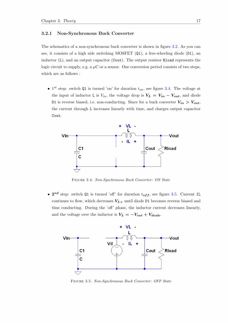
The schematics of a non-synchronous buck converter is shown in figure 3.2. As you can
see, it consists of a high side switching MOSFET (Q1), a free-wheeling diode (D1), an
inductor (L), and an output capacitor (Cout). The output resistor Rload represents the
logic circuit to supply, e.g. a µC or a sensor. One conversion period consists of two steps,
which are as follows :
• 1st step: switch Q1 is turned ’on’ for duration ton, see figure 3.4. The voltage at
the input of inductor L is Vin, the voltage drop is VL = Vin − Vout, and diode
D1 is reverse biased, i.e. non-conducting. Since for a buck converter Vin > Vout,
the current through L increases linearly with time, and charges output capacitor
Cout.
Figure 3.4: Non-Synchronous Buck Converter: ON State
• 2nd step: switch Q1 is turned ’off’ for duration toff , see figure 3.5. Current IL
continues to flow, which decreases VL+ until diode D1 becomes reverse biased and
thus conducting. During the ’off’ phase, the inductor current decreases linearly,
and the voltage over the inductor is VL = −Vout + Vdiode.
Figure 3.5: Non-Synchronous Buck Converter: OFF State
Page 31
Chapter 3. Theory 18
In continuous conduction mode the input current never drops to zero, as indicated in
figure 3.3 (left). In this case the energy is stored both in inductor L and capacitor Cout
at the end of each period T . The continuous on/off operation is called pulse-width
modulation (PWM), and the ratio of ton and toff is called duty cycle D. The output
voltage of the buck converter is determined by input voltage Vin and duty cycle D.
T =1
fsw(3.4)
ton = (D · T ) (3.5)
toff = [(1−D) · T ] (3.6)
First we derive the conversion ratio of the buck converter in CCM mode. According to
the basic inductor equation, the total change of the inductor current ∆IL is given by:
VL = L · dILdt
∴ ∆IL =
∫ t
0
VLL· dt (3.7)
For an ideal buck converter described above, the voltages over inductor L during ’on’
and ’off’ state are given above (VL,on = Vin−Vout; VL,off = −Vout+Vdiode). Ignoring the
drop over the freewheeling diode, and using equation (3.7), this yields inductor current
changes of
∆IL,on =Vin − Vout
L· ton (3.8)
∆IL,off =−VoutL· toff (3.9)
Page 32
Chapter 3. Theory 19
In steady state the current ripples during on- and off-time need to have the same size
but opposite sign, see figure 3.3. Therefore
∆IL,on = −∆IL,off
Vin − VoutL
· ton = −−VoutL· toff
Vin − VoutL
· T ·D = −−VoutL· T · (1−D)
(Vin − Vout) ·D = Vout · (1−D)
Vin ·D = Vout
D =VoutVin
(3.10)
According to equation 3.10, the output voltage of a buck converter is directly propor-
tional to the PWM duty cycle, which varies within [0;1]. Thus, if the ratio between
input and output voltage increases, the duty cycle decreases inversely.
As discussed above, in this thesis we only investigate the CCM mode of buck converters.
In this mode the inductor current always remains positive. To achieve this, the minimum
inductor current should be IL,min = Iload −∆IL
2 ≥ 0.1 · Iload [14]. Note that for strongly
varying Vin, the minimum input voltage needs to be assumed for calculating IL,min.
Consequently, the maximum current ripple ∆IL can be re-written as follows
Iload −∆IL
2≥ 0.1 · Iload
∴ ∆IL ≤ 1.8 · Iload (3.11)
The above equation (3.10) describes the conversion ratio for a perfect buck converter, ig-
noring all internal voltage drops. However, real components are never ideal. To highlight
that, figure 3.6 shows the equivalent circuit of the same buck converter, but including
some dominant parasitics. Specifically, inductor L and capacitor Cout have internal re-
sistances, indicated as RL and R_ESR (Equivalent Serial Resistance), respectively. Also,
the freewheeling diode has a forward voltage Vdiode (ignored above), which is relevant
during off-time. And finally, MOSFET Q1 has an internal resistance Rdson, which is rel-
evant during on-time. Other effects, which cause energy loss in the buck converter are
the switching of MOSFET Q1 (P = fsw ·CG · V 2G), the linear operation of the MOSFET
during switching (P = 12 · Vsat · IL · fsw · (trise + tfall)), and internal losses in the gate
Page 33
Chapter 3. Theory 20
driver. All these effects cause power loss and thus efficiency loss during buck operation,
and need to be considered in the design in order to achieve a high efficiency.
Figure 3.6: Buck Converter Schematic with Internal Capacitor and internal InductorResistance
Figure 3.7: Buck Converter Typical Wave Form [14]
To include the above described effects into VL, we would need to modify equations (3.8)
and (3.9) to
VL,on = [Vin − Vout − IL · (Rdson +RL +RESR)] (3.12)
VL,off = [−Vout + Vdiode + IL ·RESR] (3.13)
Page 34
Chapter 3. Theory 21
The dissipation due to these parasitic effects, including switching loss, is thus given by
Ploss = I2L ·[D ·Rdson + (1−D) · Vdiode
IL+RL +RESR
]+
1
2· fsw · CG · V 2
G+
1
2· Vsat · IL · fsw · (trise + tfall) + Pother (3.14)
with Pother describing other losses outside this consideration, e.g. within the MOSFET
gate driver. Consequently the efficiency of the non-synchronous buck converter is given
by the universal expression
η =Vout · Iout − Ploss
Vin · Iin(3.15)
In the case studied here, namely mean IL < 50mA, generally only switching and gate
driver loss, and the forward voltage of diode D1 in equation (3.13) are relevant. A simple
way to reduce the latter (and thus increase efficiency) is the use of a low drop diode, e.g.
a Schottky type. Another method is using an active switch, instead of a diode. This
latter option is called a synchronous buck converter, and will be discussed in the next
section.
Page 35
Chapter 3. Theory 22
3.2.2 Synchronous Buck Converter
As already mentioned above, a synchronous buck converter is an improved non-synchronous
buck converter, using an active switch instead of a freewheeling diode (see figure 3.8).
The name ”synchronous” highlights the fact that both switches (Q1 and Q2) are switched
synchronously, but oppositely.
Figure 3.8: Schematic of a synchronous buck converter
The replacement of diode D1 in figure 3.2 with transistor Q2 in figure 3.8 reduces the
power loss during the off-state of the buck converter. Specifically the loss in a diode
is IL · Vdiode · (1 − D), and the loss over an activated MOSFET is I2L · Rdson · (1 − D).
Assuming Vin = 50V, Vout = 5V (→ D = 0.1), average IL = 25mA, Vdiode = 0.7V, and
Rdson = 0.105Ω (e.g. Fairchild FDC5614P), the respective losses are 15.8mW (diode)
and 59µW (MOSFET). However, note that replacing the freewheeling diode D1 with
MOSFET Q2 adds a switching loss, which also needs to be considered. Specifically,
equation (3.14) for a non-synchronous buck converter has to be modified to (assuming
identical switches, and ignoring dead-time):
Ploss = I2L · (Rdson +RL +RESR) + fsw · CG · V 2
G+
1
2· Vsat · IL · fsw · (trise + tfall) + Pother (3.16)
Note that expression (3.15) for the efficiency remains unchanged, since it is valid for
all converters. With the above modification, the component selection can be based on
the same formulas derived for the non-synchronous buck converter. However, the most
critical issue is the synchronous control of the HS and LS switches. While the high side
switch Q1 is ON, the low side switch Q2 has to be OFF to avoid a short between supply
and GND, and vice versa. This mode is called complementary PWM operation. To
account for finite switching speed, also some delay is required between deactivating one
switch, and activation the other, the so-called ”dead time”. Figure 3.9 shows a timing
diagram for the switching of MOSFETs Q1 (PWM1H), and Q2 (PWM1L).
Page 36
Chapter 3. Theory 23
Figure 3.9: Timing of MOSFET switching for Q1 (PWM1H) and Q2 (PWM1L) fora synchronous buck converter
Since no cheap integrated buck converter control chips are currently available, the main
challenge for a synchronous converter is the generation of the dead time between high-
side and low-side switching. On one hand, it needs to be short to achieve high efficiency.
On the other hand it has to be sufficiently long to prevent a short between supply and
GND under all circumstances. To achieve this, Z.Lee has proposed an advanced control
scheme [15]. Specifically an adaptive dead time control is implemented as a digital
delay locked loop with digital counters as memory elements. While most dead time
controllers are digitally controlled, there are only few solutions for switching frequencies
above 300kHz. Besides, digital dead time controllers generally have an output jitter,
even in steady state operation. In a digital circuits, this issue can only be solved by a
very high clock speed, which interferes with IC power efficiency. As an alternative, L.Mei
has proposed an analog delay circuit [16], which uses an integrated dead-time detection
diode. According to his results, the dead time is decreased to 2ns, even though the used
gate driver TPS2832 has a dead time of 15ns. This decrease in the dead time results
in an efficiency increase from 89.2% to 90.8%. For our use-case both analog and digital
control seems suitable to generate the dead-time for a synchronous buck converter.
Note, however, that moving from a non-synchronous to a synchronous buck converter
significantly increases the complexity of the required control circuit, and thus system
cost and PCB space. For the use case investigated here, namely small ECUs with logic
currents of < 50mA, this overhead generally outweighs the efficiency gain. Specifically,
an additional power loss of 16mW (see page 22), and a CO2 fine of 3.142e/W (see page
3), would result in an advantage of 5ect of the synchronous versus a non-aynchronous
buck converter. And it seems unrealistic to implement a dead time control (plus MOS-
FET) for this money. Consequently a synchronous buck converter seems beneficial only
if other advantages exist, e.g. in case of critical temperature margins. Therefore we will
not investigate this option further in this thesis.
Page 37
Chapter 3. Theory 24
3.3 Switched Capacitor Converter
A switched capacitor DC/DC converter (”SC converter”) uses capacitors for energy
storage, instead of inductors like the buck converter discussed above. In effect, a SC
converter is a charge pump, and can step-up or step-down the input voltage. A principle
schematic of a simple SC converter is shown in figure 3.10.
Figure 3.10: Basic Switched Capacitor Structure
To step-down the input voltage, the following two steps are cyclically repeated:
• step 1: capacitors C1 and C2 are charged in series with each other through supply
Vin. This is done by opening switches SW2, SW3, SW4, and SW6, and closing switches
SW1 and SW5.
• step 2: capacitors C2, C2, and Cout are connected in parallel. This is achieved by
opening switches SW1 and SW5, and closing switches SW2, SW3, and SW6. Switch
SW4 is only required for step-up mode (see below), and remains open.
For a detailed description of charge pumps see e.g. [17]. However, for a simple overview,
assume C1=C2 and fSC (C1 ·Rload)−1. Then in the first step, the series connection
of C1 and C2 creates a capacitive voltage divider with voltage Vout = Vin2 , and energy
content E1 = C14 ·V
2in. In the second step C1 and C2 are connected in parallel between Vout
and GND, with voltage Vout = VC = Vin2 , and the energy content E2 = C1+C2
2 · V 2out =
C14 ·V
2in = E1. Thus, with ideal components circuit 3.10 would be a step-down converter
with Vout = Vin2 and η = 1. But of course, switching, ohmic and other losses result in
η < 100%.
Using a different control scheme, circuit 3.10 can also be used to step-up the input
voltage by up to ×2. For this operation mode, the following two steps are required:
• step 1: capacitor C1 is charged through the supply Vin. This is achieved by opening
switches SW2, SW4, SW5, and SW6, and closing switches SW1 and SW3.
Page 38
Chapter 3. Theory 25
• step 2: capacitor C2 is charged by C1 and supply Vin, by connecting C1 in series
with Vin (note polarity of C1). This is achieved by opening switches SW1 and SW3,
and closing switches SW2, SW4, and SW6. Switch SW5 is only required for step-down
mode (see above), and remains open.
With only two so-called flying capacitors, the above circuit is restricted to stepping up
or down the input voltage by a fixed factor of 2. However, using more capacitors, also
other factors are achievable. Specifically, using N flying capacitors in above circuit 3.10,
results in a multiplier of N , and a divider of 1N . And given a sufficiently advanced
control logic, N can vary dynamically within [2;Nmax], with Nmax given by the actual
implementation, and the N by the momentary input to output voltage ratio.
Because of their simplicity, especially for small, fixed conversion ratios and small output
currents, SC converters are widely used for low-end mobile applications, which require
efficiencies of η 90%. However, automotive applications generally have highly varying
supply voltages of typically 9V–18V, with transients reaching 40V. Also most ECUs re-
quire an additional quiescent mode with Iin < 100µA. Covering these requirements with
a SC converter and high efficiency requires a complex control logic, which dynamically
selects the optimum number of flying capacitors, and also switching frequency fSC . In
the past this has prevented the widespread adoption of SC converters in automotive
electronics.
However, new incentives in the automotive industry caused by high fuel prices and CO2
legislation have increased interest in all efficient supply concepts, including SC converters
[18]. And compared to buck converters, the switched capacitor concept indeed has
several advantages:
• small footprint on PCB
• low cost passive components
• high energy density of capacitors vs. inductors
• complex control logic gets cheaper with semiconductor progress
The potential of SC converters using modern CMOS processes was investigated in detail
by V. Ng and S. Sanders [19] in 2010. Specifically they developed an integrated chip in a
180nm, triple-well CMOS process by TSMC1. This IC integrates all power switches, and
also the required control logic. The flying capacitors are external SMD components on a
standard PCB. The complete SC converter has an input voltage range of 7.5V to 13.5V,
a fixed output of 1.5V, and an output current range of 5mA to 1A with an efficiency of
80% to 92% within the working range.
1http://www.tsmc.com/english/default.htm
Page 39
Chapter 3. Theory 26
The block diagram of the implemented IC is shown in figure 3.11. The principle is the
same as in above figure 3.10, but here the (maximum) number of flying capacitors are 8,
instead of 2. Using a complex feed-forward and -backward control, the IC automatically
determines the optimum number of C’s (from Vout/Vin), and also fSC (from Iout). Using
different voltage domains with level-shifters, they managed to allow for Vin ≤ 13.5V,
using a 5V standard CMOS process (→ low IC price). In their final assessment V. Ng
and S. Sanders conclude that for their targeted (mobile) applications the SC concept is
at least comparable to a buck converter, also including component price.
Figure 3.11: Switched capacitor IC by V. Ng and S. Sanders [19] [20]
However, in this thesis we target supply concepts for automotive and light e-mobility
applications. As mentioned above, these have additional requirements, which need to
be met. These requirements, and their impact on the SC concepts are as follows
• standard automotive supply voltage is 9V–18V, with transients reaching 40V. For
e-mobility supply voltage goes up to 60V
Page 40
Chapter 3. Theory 27
– with 5V CMOS process, V maxin = 60V requires ≥35 flying capacitors and
corresponding power switches. This increases the cost for the IC, for the
external components, and increases the PCB footprint
– using a high-voltage semiconductor process (V maxDS 5V), e.g. BCD or HV-
CMOS, decreases the number of required voltage steps. However, this de-
creased the output granularity (∝ 1/N), and also increases the IC area price
• extreme EMC requirements for emission and robustness
– SC efficiency is mostly dominated by the resistance of the power switches.
However, a very low Rdson increases the peak current into the ”top” flying
capacitors (C7 and C8 in figure 3.11). Due to very low emission limits, the
switching noise of the SC converter most probably needs to be LP-filtered
inside the ECU, which increases price and PCB footprint
• high cost pressure, especially for low-end ECUs
– the size of the final IC in [19] is 3.3× 3.5mm2. At an estimated volume price
of ∼5–8ect/mm2, this corresponds to an IC cost of ∼58–92ect.
– in technical discussions, both experts from Dialog Semiconductor2 and Infi-
neon Technologies3 agreed that in a modern process the size of any similar IC
is dominated by the power switches. While these can be reduced slightly using
a BCD process, they do not shrink with technology. Both experts agreed that
this limits the competitiveness of the SC concept for automotive applications.
2http://www.dialog-semiconductor.com3http://www.infineon.com
Page 41
Chapter 3. Theory 28
3.4 Closed Loop Control and Compensation Technique
In the above sections, we have motivated our decision to concentrate on the buck con-
verter concept. Specifically this seems most suited to reach the target of this thesis,
namely identifying a cheap and efficient converter design. In this section we will now
discuss the regulation loop for this converter type. All DC/DC converters require a
closed loop regulation in order to keep the output voltage Vout within a specified range.
This control mechanism asserts a fixed output voltage by adjusting the duty cycle D to
changes in input voltage (Vin), and load current (Iload). As explained previously, a buck
converter consists of two main parts, namely power stage and control stage. Figure 3.12
shows a simple buck converter, including the closed control loop, and the driver stage.
The control stage regulates the output voltage by modulating the duty cycle via the
feedback control circuit, and switching Q1 via the driver. The input for this control loop
is Vout, and the output is the duty cycle D for the power stage, i.e. switch Q1 (and op-
tionally Q2). This kind of control is called voltage controlled mode (VCM), in contrast to
current control mode (CCM), which uses IL as input for the control loop. The challenge
in designing the control loop is to find an adequate loop gain margin (GM) and phase
margin (PM) within the required frequency domain. In the following subsection, we will
analyze control loops with different compensation types, together with their respective
circuitry.
Figure 3.12: A simple Buck Converter Control Algorithm
There are three compensation schemes for the above error amplifier, which are mostly
used by the design engineers. These control techniques are known as type 1, type 2,
and type 3 control. Of these, type 1 compensation is rarely used, mainly because of
Page 42
Chapter 3. Theory 29
inferior frequency margin. However, below we will describe each compensation type
with implementation, and respective advantages, and disadvantages.
3.4.1 Type 1 Control
Type 1 control is performed using an integral control operational amplifier, which is
shown in figure 3.13. The system starts working as soon as there is a difference between
output and reference voltage (Vout and Vref ). The voltage divider consisting of R1 and
R2 is used to scale the output voltage to the reference voltage. Besides, it has no effect
on the compensation network. The error transfer function, and the (unity) gain of this
system is given by equations 3.17 and 3.18, respectively.
Figure 3.13: Type 1 Control Schematic
VerrVout
= − 1
R1 · C1 · s(3.17)
Funitygain =1
2π ·R1 · C1(3.18)
As shown in figure 3.14, type 1 compensation has only one pole, its gain decreases with
frequency by -20dB/decade, and it has a constant phase shift of -90. Therefore the
only degree of freedom is the unity gain frequency.
Page 43
Chapter 3. Theory 30
Figure 3.14: Type 1 Bode Plot for phase shift and gain margin
3.4.2 Type 2 Control
Type 2 control is an improvement over type 1, which is achieved by adding one resistor
and one capacitor. The type 2 schematics is shown in figure 3.15. Compared to type 1,
this control has improved by one additional pole and one zero.
Figure 3.15: Type 2 Control Schematic
In this type, the control loop shows a phase boost, with the compensator achieving its
maximum phase at the zero crossing frequency Fzero, and the second pole frequency
Fpole. This behavior is shown in figure 3.16.
Type 2 compensation commonly used, because of the above described phase boost ad-
vantage [21]. To take full advantage of this feature, specifically to reject lower harmonics
of the switching frequency, the crossover frequency has to be between the zero and the
pole. A detailed description for achieving this, is given by D. Venable in [22] and [23].
In the type 2 schematics shown in figure 3.15, R1 and C1 provide the poles on the gain
origin, and R2 and C2 provide the zero. The error transfer function of this control is
Page 44
Chapter 3. Theory 31
Figure 3.16: Type 2 Bode Plot for phase shift and gain margin
given by equation 3.19
VerrVout
= − 1
s ·R1 · (C1 + C2)× (1 + s · C2 ·R3)(
1 + s ·R3 · C1·C2C1+C2
) (3.19)
If C2C1, the transfer function 3.19 can be approximated by
VerrVout
= − 1
s ·R1 · C2× (1 + s · C2 ·R3)
(1 + s ·R3 · C1)(3.20)
For this case (C2C1), the bode plot with phase shift and gain is shown in above figure
3.14. For this we can calculate the pole (Fpole ) and zero crossing frequency (Fzero)
using below equation 3.21 and 3.22, respectively. And for these pole and zero, the gain
is given by equation 3.23
Fzero =1
2π ·R3 · C2(3.21)
Fpole =1
2π ·R3 · C1(3.22)
∣∣∣∣VerrVout
∣∣∣∣midgain
≈ −R3
R1(3.23)
The main advantage of type 2 control is the 90 reduction in phase shift compared to
type 1 compensation. In addition, this control type has more degrees of freedom, namely
selection of Fzero, Fpole frequency, and the midspan gain.
Page 45
Chapter 3. Theory 32
3.4.3 Type 3 Control Method
Type 3 control is an improvement over type 2 compensation, which adds an additional
pole and an additional zero to the system. The zeros and poles are usually located at
Fzero and Fpole, which have already been described in the above type 2 compensation.
Because of this, we have an extra 90 phase boost with respect to type 2 compensa-
tion control. This additional phase boost provides a higher loop cross over frequency
(i.e. higher bandwidth), compared to type 2 compensation scheme. The basic schematic
and corresponding bode plot of a type 3 control are shown in figures 3.17 and 3.18,
respectively.
Figure 3.17: Type 3 Control Schematic
Figure 3.18: Type 3 Bode Plot for phase shift and gain margin
Page 46
Chapter 3. Theory 33
The error transfer function of type 3 control method is given by equation 3.24
VerrVout
= − 1
s ·R1 · (C1 + C2)× (1 + s · C2 ·R3)(
1 + s · C2 ·R3 · C1·C2C1+C2
) × (1 + s · C3 · (R1 +R4)
(1 + s · C3 ·R4)(3.24)
If C2C1, the transfer function 3.24 can be approximated by
VerrVout
= − 1
s ·R1 · (C1 + C2)× (1 + s · C2 ·R3)
(1 + s · C1 ·R3)× (1 + s · C3 · (R1
(1 + s · C3 ·R4)(3.25)
Compared to type 2 compensation, this method has more degrees of freedom, and in
addition has one more Fpole and Fzero. These zeros and poles are given by equations
3.26. To achieve maximum regulation stability, the frequencies of the zeros and poles
have to be identical, i.e. Fzero1 = Fzero2, and Fpole1 = Fpole2.
Fzero1 ≈1
2π ·R3 · C2
Fzero2 ≈1
2π ·R1 · C3
Fpole1 ≈1
2π ·R3 · C1
Fpole2 ≈1
2π ·R4 · C3(3.26)
The corresponding gain the frequency Fzero1 (= Fzero2) are given by equation 3.27, and
the gain at frequency Fpole1 (= Fpole2) is given by equation 3.28∣∣∣∣VerrVout
∣∣∣∣f=Fzero1
≈ 2 ·R3
R1(3.27)
∣∣∣∣VerrVout
∣∣∣∣f=Fpole1
≈ R3 · C2
2 ·R1 · C1(3.28)
Page 47
Chapter 3. Theory 34
3.4.4 Feedback Control
As already mentioned above, there are two common feedback modes, namely voltage
mode control (VMC) and current mode control (CMC). In voltage mode control, the
output regulation of the converter is achieved by an error amplifier and a voltage com-
parator, which are shown in figure 3.14. In VMC the duty cycle is controlled by the
output of the error amplifier, which is the amplified difference between Vref and VF . In
current mode control, both inductor current IL and output voltage VF are regulated via
an internal control loop. A simplified schematics of a current mode control feedback is
shown in figure 3.19.
Figure 3.19: Current mode control circuit [24]
A comparison of CMC and VMC feedback operation shows the following differences
• CMC mode has two internal control loops, which yields in a more robust regulation
compared to VMC, especially in cases with large output load jumps. Therefore,
most modern integrated control ICs use current mode controlled feedback topolo-
gies.
• in CMC, the output voltage drop can be reduced by around 25%, and the settling
time reduced by around 36%. This improves the dynamic response of CMC with
respect to VMC mode [25].
• the main disadvantage of CMC is the additionally requires current sense circuit.
This causes additional loss, decreases the overall efficiency, and adds cost.
Page 48
Chapter 3. Theory 35
Since no cheap integrated control chips are currently available on the market, we have
to implement a discrete control loop. Therefore we have chosen VMC mode, to avoid
the additional sensing required for CMC mode.
Page 49
Chapter 4
Concept and Implementation
All DC/DC converters discussed in the preceding chapters require different control and
power stages. To design these optimal for a given application, many parameters need to
be considered, like input- and output voltage and current range, input- and output rip-
ples, efficiency, transient output response, automotive or non-automotive requirements,
converter size, safety and protection features, switching frequency range, etc. Changes
in any of these parameters will immediately effect efficiency, price, robustness, and life-
time of the DC/DC converter. As discussed in chapter 3, due to cost and space reasons
this thesis focuses on non-isolated synchronous and non-synchronous buck converters.
For these we will theoretically derive selection criteria for all relevant components in
this chapter, namely inductor (L), MOSFET (Q1 and Q2), output capacitor (Cout), and
free-wheeling diode (D1). In addition we will derive suitable control and power stage
parameters, as well as the expected power efficiency.
4.1 Component Selection for Buck Converter
4.1.1 Inductor Selection
Choosing the correct inductor for a buck converter is one of the most critical issues
to achieve high efficiency, acceptable inductor size (and thus price), and a low output
voltage ripple. In the buck converter, the inductor acts as an energy storage component.
Principally, when switch Q1 is turned on, the current in the inductor starts to increase.
The energy stored in the B-field of the inductor at the end of the ON time is equal to
E = 12 · (L · I
2) where L is the inductance and I is the inductor peak current. The
simplified equivalent circuit and transient voltages and currents are shown in figures 4.1
and 4.2, respectively.
36
Page 50
Chapter 4. Concept and Implementation 37
Figure 4.1: Buck converter representation during ON time
Figure 4.2: Inductor voltages and current during ON and OFF time
As shown in figure 4.2, the inductor current increases gradually during the ON time of
the PWM period (0 to D×T). Under the assumption of linear operation, this change in
the inductor current, or ripple current ∆IL+, can be calculated using equation 4.1.
VL = L · ∆IL+
∆t(4.1)
with VL = Vin − Vout the voltage drop over the inductor (see fig. 4.1), and ∆t = tON =
D × T the ON time. Using these, the ripple current ∆IL+ becomes
∆IL+ =(Vin − Vout)
L·D · T =
(Vin − Vout)L · fsw
·D (4.2)
∴ L =(Vin − Vout)∆IL+ · fsw
·D (4.3)
Thus, for fixed input and output voltages, load current, and switching frequencies, we
Page 51
Chapter 4. Concept and Implementation 38
can calculate the required inductance value using equation 4.3. For example assume an
application with the following requirements
• Output voltage → Vout = 6V
• Input voltage → Vin,max = 60V
• Duty cycle → D = VoutVin,max
= 660 = 0.10
• Load current → Iload = 20mA → ∆IL+ ≤ 1.8 · Iload ≈ 35mA (see eq. 3.11)
• Switching frequency → fsw = 150kHz (compromise btw. switching loss and EMC)
Using above equation 4.3, the minimum required inductance value is
L =(Vin,max − Vout)
∆IL+ · fsw·D =
(60− 6)
35× 10−3 · 150× 103· 0.1 = 1.02mH (4.4)
Consequently, for the above example application, an inductor value of ≈1mH is suited,
preferably with a low internal resistance, in order to achieve high efficiency. Note that
this inductor is equally suited for non-synchronous and synchronous buck converters. In
our design, we have used a 1.02mH inductor by Coiltronics1.
4.1.2 MOSFET Selection
Because of its electrical and thermal impact, and its effect on the required power stage,
selecting the optimum components for switches Q1 and optional Q2 is more complex than
choosing an inductor using above equation 4.4. In most buck converter designs these
switches are realized as MOSFETs (Metal Oxide Semiconductor Field Effect Transis-
tor), due to their superior dynamic switching behaviour. Because of the complex inter-
dependencies, we will first briefly explain the MOSFET working principle, and later the
selection criteria for a buck converter.
The principle structure of a MOSFET is shown in figure 4.3. Generally it has four
terminals, specifically Drain (D), Gate (G), Source (S), and Body (B). The body terminal
is often common with the source terminal, which is why most MOSFETs have only
the three terminals D, G, and S. Basically a MOSFET behaves like a (highly non-
linear) voltage controlled resistor. Specifically, the resistance RDS between drain and
source, and hence the current IDS or ID between drain and source, can be changed by
several orders of magnitude via gate-source voltage VGS . This effect is achieved by the
Page 52
Chapter 4. Concept and Implementation 39
Figure 4.3: MOSFET structure with Drain (D), Gate (G), Source (S) and Body (B)[26]
generation and depletion of a conducting channel beneath the gate, which is located
between source and drain.
Similar to bipolar transistors, MOSFETs also have two variants, namely p-type (p-
channel or pMOS) and n-type (n-channel or nMOS). These two types of MOSFET
differ in the utilization of the substrate. For both nMOS and pMOS transistors, there
exist two variants, which differ in the internal structure, and their electrical properties:
• Enhancement → self-locking (off if no VGS applied)
• Depletion → self-conductive (on if no VGS applied)
For safe off state, and since the depletion typ is only rarely used (and thus expensive),
we will here focus on enhancement type MOSFETs
In nMOS enhancement type transistors, heavily n-doped source and drain structures are
embedded in a lightly p-doped substrate (=body) region. As the name MOSFET implies,
the conducting gate is isolated from the body by a thin oxide, effectively resulting in
a capacitor with terminals G and B. Without applied VGS , two opposite diodes form
between S/B and B/D, preventing current flow between S and D. If a positive voltage
VGS is applied between gate and source, negative charge carriers (i.e. electrons) are
forced into the channel underneath the gate, where they recombine with the positive
holes, effectively decreasing the doping of the channel. If the channel becomes negatively
charged, the diodes vanish, and current can flow via the conduction of electrons in the
channel (hence nMOS). This voltage is called the treshold voltage Vth of the transistor.
At yet higher VGS , the channel is flooded with more electrons (→ decreasing RDS), until
saturation is reached. The (minimum) resistance in this state is called Rdson.
1http://www.cooperindustries.com
Page 53
Chapter 4. Concept and Implementation 40
In contrast, pMOS enhancement type transistors consist of p-doped source and drain,
and an n-doped channel. Here, IDS consists of positively charged holes with a compar-
atively low mobility. Consequently a negative VGS has to be applied to force positive
holes into the channel, and thus switch on the MOSFET.
In integrated digital circuits, both MOSFET types are commonly used together to form
a complementary MOS (or CMOS) element.
The equivalent circuit of a pMOS is shown in figure 4.4. As can be seen, gate terminal (G)
is connected to drain (D) via gate resistance (RG), and capacitor (CGD). In addition,
gate (G) is connected to source (S) via parasitic capacitance (CGS). Also, drain (D)
is connected to source (S) via parasitic capacitance (CDS) and a current sink. And,
finally, body (B) is connected to drain (D) via the so-called body diode. There are
also parasitic inductances between drain and current sink, and source and current sink,
which are mainly due to the required bond-wires. In the following these inductances will
be neglected, in order to simplify the explanation of the fundamental functionality.
Figure 4.4: Equivalent Circuit of PMOS Device
While the parasitic capacitances CGS , CGD, and CDS in figure 4.4 are crucial to DC/DC
switching performance, they are typically not specified by the manufacturers. Instead
mostly only capacitances CISS , CRSS , and COSS are given, which have to be converted
to the required Cx in figure 4.4 using the following equations
CDS = COSS − CRSS (4.5)
CGS = CISS − CRSS (4.6)
CGD = CRSS (4.7)
Page 54
Chapter 4. Concept and Implementation 41
In DC/DC converter design, MOSFET parameters source-drain resistance (Rdson), gate
capacitance (CGD), switching thresholds, temperature dependence all effect the opera-
tion, and thus efficiency of the overall system. Therefore, designers have to take special
care to select a suitable component.
The source-drain resistance Rdson has a direct impact on ohmic losses during ON (Q1),
respectively OFF phase (Q2), within the PWM period. The average ohmic power loss
in Q1 is given by PMOSFET (ON) = Rdson × I2L ×D. Therefore, a low Rdson results in a
low the power loss.
As mentioned before, n- and p-channel MOSFETs have different properties. Specifically,
due to the higher mobility of electrons compared to holes, nMOS transistors have a lower
Rdson than a pMOS type of identical size. Consequently, for a given Rdson, generally
nMOS are cheaper than pMOS.
On the other hand, as described above, switching a nMOS requires a voltage of VGS >
VS + Vth. While this is generally uncritically for a low-side MOSFET (VS = GND),
switching a high-side nMOS requires VGS > Vbat + Vth, and therefore a step-up circuit,
e.g. a bootstrap or charge-pump. In contrast, a pMOS can is switched on by applying a
negative VGS , which is easily realized using an open-drain switch to GND.
So, for a given application, the designer has decide which MOSFET type, Rdson, and
corresponding driver circuit is most suited for the respective project. Apart from the
above loss, also the maximum allowed Vds has to be considered, which has to be higher
than the maximum input voltage of the system.
In addition to the above ohmic losses, switching, and transition losses also need to be
taken into account when selecting a MOSFET for a given application. As derived in
equation 3.14, the losses in MOSFET Q1 are given by
Ploss = I2L ·D ·Rdson +
1
2· fsw ·
[CG · V 2
G + Vsat · IL · (trise + tfall)]
(4.8)
These losses have to be minimized (at acceptable cost) by using MOSFETS with both
low Rdson and low CG. The latter is also important to reach fast switching times, since
trise and tfall are directly proportional to CG.
An additional parameter, which is important in MOSFET selection is its operating
temperature range. There are two major temperature parameter in the MOSFET cal-
culation, namely maximum junction temperature (Tj), and ambient temperature (Ta)
for the MOSFET. According to a Fairchild application note [27], the junction temper-
ature of the MOSFET device is Tj = Ta + (Ploss × ΘCA) for a packaged device, and
Tj = Ta + (Ploss × ΘSA) for a bare die, with ΘCA the thermal resistance between case
Page 55
Chapter 4. Concept and Implementation 42
and ambient, and ΘSA the thermal resistance between heat sink and ambient. Both ex-
pressions neglect the (very small) thermal resistance between die and case, respectively
die and heat sink.
Summarized, the following considerations have to be taken into account when selecting
a MOSFET for a non-synchronous or synchronous buck converter design:
• Decide type of MOSFET (either n-channel or p-channel) with respect to the re-
quirements of the project.
Note: n-channel requires external drive circuit which adds cost. P-channel MOS-
FET can be driven by a level translator with a NPN bipolar transistor, which is
cheaper than driving the n-channel.
• Select maximum Vds (= breakthrough voltage) suitable for the input voltage re-
quirements.
• Select low Rdson value to minimize power losses.
• Consider Qg, Qgs, Qgd for MOSFET. Specifically CG (and thus Qg) should be
minimized to increase switching speed, and thus decrease switching losses
• Assert that ambient and junction temperature do not exceed operational temper-
ature range of the MOSFET. If necessary, improve cooling on PCB or to case.
Mainly to minimize driver cost, the simulation and the corresponding experimental setup
uses a p-channel MOSFET, which is switched on via a level translator, and switched
off via a pull-up resistor to Vin. We have selected the pMOS FDC5614P by Fairchild2,
which has Rdson = 0.105Ω, and gate charge CG = 15nF . Note that due to switching-off
via a pull-up resistor, special emphasis has to be put on using a MOSFET with a low
CG.
4.1.3 Output Capacitor Selection
The output capacitor Cout shown in figure 3.6 has to be selected according to the output
ripple requirements. As discussed before, Cout internally also has a parasitic series resis-
tance (ESR), and a small inductance (ESL). The biggest losses in the output capacitor
are caused by these parasitics ESR and ESL. The main purpose of the output capacitor
in the power stage is to minimize the output voltage ripple for the load. The current
2http://www.fairchildsemi.com
Page 56
Chapter 4. Concept and Implementation 43
into the capacitor is dependent on the voltage ripple, which in the linear approximation
can be calculated by using eq. 4.9
Ic = Cout ×dv
dt(4.9)
with dv the voltage ripple, Ic the ripple current to the capacitor, and dt the switching
period.
For a buck converter in steady state, the current into the capacitor during ON time
(charging, +ve) has to be equal to current out of the capacitor during OFF time (dis-
charging -ve) → Ic = 0. In this state the change in capacitor charge during a PWM
period is given by
∆QC = C ×∆VC (4.10)
On the other hand the change in the current during the charging phase is equal to the
area under the triangle which shown in figure 4.5, and is equal to
∆QC =1
2× Tswitch
2× ∆IL
2(4.11)
Figure 4.5: Capacitor Charge and Discharge waveform
Setting equations 4.10 and 4.11 equal finally yields an expression for the voltage ripple
as a function of capacitance, switching speed, and ripple current.
∆V =Iripple · T
8 · C=
Iripple8 · C · fsw
(4.12)
With a load current of 20mA (→ Iripple ≤ 35mA), a switching frequency of 150kHz, and
a maximum voltage ripple of 100mV (see table 2.1), equation 4.12 directly yields the
Page 57
Chapter 4. Concept and Implementation 44
minimum required capacitance:
C =Iripple
8×∆V × fsw(4.13)
C =35 · 10−3
8× 100 · 10−3 × 150 · 103F (4.14)
C = 2.9 · 10−7F ≈ 0.3µF (4.15)
Since above capacitance value is the minimum value, we can select a TDK3 tantalum
1µF capacitor with 8mΩ ESR resistance. If possible, it is recommended to use two
capacitors, in order to reduce the ESR and increase the capacitance, which in turn
minimizes the ripple on the output voltage. This capacitor value can be used both in
non-synchronous and synchronous buck converters.
4.1.4 Free Wheeling Diode Selection
Careful selection of the free wheeling diode is also important to minimize power dissi-
pation in non-synchronous buck converters. In synchronous buck converters, diode D1
is replaced by low-side switch Q2, so this section is irrelevant for that concept.
In addition to choosing a low drop diode to minimize losses during the OFF phase, it
has to be asserted that the input voltage does not exceed the maximum reverse voltage
of the diode, and also that the peak and average diode currents are within its operating
limits. The latter are given by
ID,pk = Iload,max +Iripple
2(4.16)
ID,av = Iload,max × (1−D) (4.17)
To minimize the power loss, Schottky diodes can be used since these have a low forward
voltage drop, allow fast switching, and have high peak and average current rating.
For a given diode, the power loss in the diode is given by
PD = ID,av × VF (4.18)
with VF the forward voltage drop of the selected diode.
3http://www.tdk.com
Page 58
Chapter 4. Concept and Implementation 45
In our design, we have used Schottky diode MBRS360 by ONSemi4, which has a maxi-
mum reverse voltage of 60V, and a maximum current of 3A.
4.2 Switching Frequency Selection for Buck Converter
In switched direct current to direct current (DC/DC) conversion, there exists a trade-off
between switching frequency, component size, transient response, switching ripples, etc..
Specifically, a high switching frequency allows smaller inductors and capacitors, but in
creases switching loss, and requires a stronger driver stage. A wrong switching frequency
can impact on power loss, output ripples, and even the DC/DC conversion ratio.
With the advent of specific ICs for switched converters in the last decade, a trend exists
towards DC/DC converters with high frequencies in the MHz range. Driver for this is
the urge to decrease passive component size (and cost), and thus reduce PCB space,
and even facilitates new products, previously impossible, e.g. ultra-thin smartphones.
However, as equation 3.14 shows, high switching frequencies have a negative impact on
switching losses, and can cause EME issues.
In this section, we examine how select the optimum switching frequency for a given
application. As already discussed in chapter 3, the output voltage of a buck converter
is Vout = Vin×D, with D the PWM duty cycle. This duty cycle is defined as D = TONT .
As already mentioned above, a high frequency lowers the size of passive components L
and Cout, but increases the AC power loss in transistor(s) and diode. The latter is due
to the reverse recovery time, which causes additional losses in the freewheeling diode.
A.Prisman explains this situation in his book as follows [14]: ”The more switching
transitions there are in a particular period, the more switching loss there will be as
a result there is trade of decreasing the switching period T (increasing the switching
frequency) may well decrease the size of the filter elements, but it will also add to the
total losses and may require a larger heat sink. In general, although the overall volume of
the buck regulator will be lower at a high frequency, the increase in the switching loss and
the more stringent high frequency layout and component selection requirements make the
final choice a compromise among all the opposing elements”. In his book [14] A.Prisman
also connection between switching frequency and EMC issues. But, as always, the final
frequency selection is up to engineer.
As mentioned above, we have chosen a very simple driver stage, which switches off Q1 by
a pull-up to Vin. The schematics will be given and discussed in chapter 5, but in order
to reach our efficiency goal of η ≥ 70%, this pull-up must not be too low-ohmic. On
4http://www.onsemi.com
Page 59
Chapter 4. Concept and Implementation 46
the other hand, this pull-up together with the gate capacity CG constitute an RC filter,
which limits the switch-off speed. In our design, we have therefore limited the switching
frequency to fsw ≤ 150kHz.
4.3 Compensation Network for Buck Converter
In this section, we will briefly explain, why we decided to use a type III compensation
network for the buck converter regulation loop. In addition, we will give the rules for
the component selection for the error amplifier, based on the given requirements.
As shown in section 3.4.1, type I compensation has only one pole, and it also does not
enhance the compensation network. Type II and type III on the other hand enhances the
compensation by adding a single pole and a zero, or two zeros and two poles, respectively.
For our design we have selected type III compensation, because of it’s superior system
behavior with respect to stability and dynamic response. And this improved behavior is
achieved by adding one small, low-voltage capacitor, i.e. at virtually no additional cost.
As already explained in the previous chapter, a small change in the Vout is being sensed
by the error amplifier via resistor Rload (called ”sampling network” if realized as a voltage
divider with two resistors). This voltage is compared with the reference voltage Vref
at the non inverting input in the error amplifier. The reason for using a compensation
network in the error amplifier is to cancel the effects of the LC output filter resonance
in the power stage. Thus the component selection for the error amplifier is critical to
achieve a stable output voltage.
The below given rules assist in achieving a stable output voltage, if applied correctly.
Note that section 6.4, gives an analysis of the small signal (i.e. AC) behavior of the
proposed circuit, which is important for understanding the phase margins and gain
margins. These have already been theoretically derived and discussed in chapter 3, and
it is strongly recommended to fully understand the small signal behavior of the power
stage and compensation network, before designing a buck converter.
Page 60
Chapter 4. Concept and Implementation 47
Component Selection for Type III Compensation
• Step 1: Calculate gain bandwidth for the large signal stability. In an ideal case
Nyquist theorem demands 1/10 of switching frequency
fC =fsw10
=150000
10= 15kHz (4.19)
with fC the crossover frequency. In real applications, fC has to be at least half
of the switching frequency, but in practical cases, 1/4 or 1/5 of the switching
frequency is reasonable
• Step 2: Calculate the zero frequency for 45 phase margin
R1 · C1 =1
2πfC= 1.06× 10⁻⁵ (4.20)
where R1 input Z of operational amplifier. To reach fC = fsw10 for the selected
switching frequency, we have chosen R1 = 8.5kΩ, and C1 = 1.247nF.
• Step 3: Select R2/R1 to achieve unity gain (i.e. max. phase boost) for f = fC
K =R2
R1=
(2πfc)2VPLC
Vin(4.21)
R2 =(2πfc)
2VPLCR1
Vin= 42.5kΩ (4.22)
K =R2
R1=
42.5
8.5= 5 (4.23)
• Step 4: Calculate zero DC error and low frequency gain
ωn =
√1
LCout= 31.311 (4.24)
with ωn the low-frequency gain, and C2 >10
ωn·R2= 7.5nF
• Step 5: Choose R2 · C3 = ESRout · Cout to avoid effects of the equivalent series
resistor
ESRout = 0.102Ω (4.25)
C3 =ESRout · Cout
R2= 2.4pF (4.26)
According to the above component selection, our compensation circuit parameters are
like shown in the table 4.1;
Page 61
Chapter 4. Concept and Implementation 48
Parameter Value Unit
L 1.02 mH
Cout 1 µF
Cout1 0.5 µF
Cout2 0.5 µF
fsw 150 kHz
Rb 2 kΩ
Rgs 500 Ω
ESRout 0.102 Ω
R1 8.5 kΩ
R2 42.5 kΩ
C1 1.247 nF
C2 7.5 nF
C3 2.4 pF
fc 15 kHz
Table 4.1: Components for Compensation and Power Stage
Page 62
Chapter 5
Methods
As discussed in chapters 3 and 4, the most promising concept for a cheap, efficient low-
end supply (today) is a buck converter with discrete regulation and power stage. This
is mainly due to the absence of suitable ICs on the market. In the previous sections we
have already motivated the selection of control network and components.
To investigate the proposed concepts, we have performed a multitude of SPICE simu-
lations, which were validated independently by an experimental setup. All simulations
were performed using Orcad PSpice 9.11 and LTSpice version 4.6d2. In the next two
subsection, we will first present the simulation and hardware setup for the experimental
validation of the models. Then we will show the simulation models for the proposed
synchronous and non-synchronous buck converter designs.
5.1 Experimental Validation
Since this thesis heavily relies on SPICE simulation results, special emphasis has been
placed on experimental validation of the simulation setup. Specifically we have imple-
mented a non-synchronous buck converter in SPICE, and also as hardware on a bread
board.
1http://www.cadence.com/us/pages/default.aspx2http://www.linear.com/designtools/software/
49
Page 63
Chapter 5. Methods 50
For the validation we have used the following components and parameters
• inductor L: SLF7045T-681MR20-PF by TDK3 with 680µH inductance and series
resistance of 1.48Ω
• HS-switch Q1: IPD50P04P4-13 40V p-channel MOSFET by Infineon4 with Rdson =
12.6mΩ, QGS = 17nC.
• switch-on Q1: bipolar npn transistor
experiment: BCY58X by NXP5 with maximum VCE = 32V
experiment: 2N3019 by Semicoa6 with maximum VCE = 80V
• switch-off Q1: pull-up between gate and source of Q1 with 100.8Ω
• zener diode: BZX84C12L by ONSemi7 with 12V breakthrough voltage
• diode D1: MBRS360 Schottky diode by ONSemi with a forward voltage of 0.3V
• output capacitor Cout: 22µF electrolyte capacitor
• input capacitor C1: 10µF electrolyte capacitor
• switching frequency fsw: 100kHz
• input voltage Vin: 15.5V
• output voltage Vout: 5V
• load simulation: output resistor with 10.9Ω
As shown above, the only difference between simulation and experiment is the type of
npn transistor for switching Q1, which is not critical for operation.
The simulation model is shown in figure 5.1, and the identical, experimental setup is
shown in figure 5.2. The simulated and experimental behavior will be compared and
discussed in chapter 6.
3http://www.tdk.com4http://www.infineon.com5http://www.nxp.com6http://www.semicoa.com7http://www.onsemi.com
Page 64
Chapter 5. Methods 51
Figure 5.1: Simulation Model of Validation Circuit
Figure 5.2: Hardware Set-Up of Validation Circuit
Page 65
Chapter 5. Methods 52
5.2 Simulation Models
As discussed in the previous chapters, a buck converter consists of three stages, namely
power, compensation, and control stage. All of these stages have been investigated the-
oretically in chapter 3, and the component values derived according to the requirements
(see table 4.1).
The simulation models for both synchronous and non-synchronous buck converter have
been set-up identically, where applicable. Specifically, both use a type 3 compensation,
as discussed above. Switching on of the high side power MOSFET FDC5614P by
Fairchild8 is performed by an n-channel bipolar 2N5210 transistor, also by Fairchild
with a level translator. Switching off is performed by a pull-up resistor between gate
and source. To reduce the effect of ESRout, the output capacitor Cout was split into
two identical capacitors with Cout1 = Cout2 = Cout2 . To protect Q1 agains over voltage, a
zener diode BZX85C15L by Vishay9 is placed between gate and source. An additional
soft start feature has been implemented in the circuit, in order to avoid overshoots.
Essentially it is a low-pass filter for Vref with Ros = 1.2kΩ and Cos = 1µF.
8http://www.fairchildsemi.com9http://www.vishay.com/
Page 66
Chapter 5. Methods 53
The non-synchronous buck converter uses a MBRS360 Schottky diode by OnSemi10 as
freewheeling diode D1. Selecting a Schottky diode reduces the forward voltage from
∼0.7V to ∼0.3V. This in turn reduces the power loss in the OFF phase, and thus
increases overall efficiency. The resulting schematic for the non-synchronous buck-
converter, including proposed components, is shown in figure 5.3.
Figure 5.3: Non-Synchronous Buck Converter Schematic with Compensation Network
10http://www.onsemi.com
Page 67
Chapter 5. Methods 54
In the synchronous buck converter, diode D1 is replaced by an active switch. For simplic-
ity we have used the same Fairchild FDC5614P for low-side switching, as for high-side
switching. The driver circuit is also identical, but requires an additional inverter for
opposite switching. The resulting schematic for the non-synchronous buck-converter,
including proposed components, is shown in figure 5.4.
Figure 5.4: Synchronous Buck Converter Schematic with Compensation Network
The above SPICE models have been used to extensively investigate the behavior and
properties of the simulated circuits. Specifically we have performed analyses of static,
transient and small signals, overall efficiency, and also conducted EMC emission. The
results will be presented and discussed in chapter 6.
Page 68
Chapter 6
Results and Discussion
In this chapter, the results from simulation and experimental validation will be presented
and discussed. Initially we will quantitatively compare the results of the test circuit
as obtained from simulation (see figure 5.1), and experiment (see figure 5.2). After
validation of the simulation setup, we will present the simulation results for the non
synchronous and synchronous buck converters. Specifically we will show the dynamic
behavior for both converter types, as well as the transient response and small signal
analysis.
6.1 Experimental Validation
In this section, the dynamic responses of a non-synchronous buck converter in simulation
and actual experiment will be compared. For the experiment, an input voltage of 15.5V
and a target output voltage of 5V are used. Correspondingly a duty cycle of ∼ 32%
was set manually (D = VoutVin
= 515.5), and the switching frequency of fsw = 150kHz is
generated using a frequency generator. The simulation and hardware circuits used are
shown in figures 5.1 and 5.2, respectively.
To check the validity of the simulation model, input PWM signal VPWM , resulting gate
voltage Vgate, drain voltage Vdrain, and finally output voltage Vout are compared in the
time domain. In the experimental setup, these values were obtained from saving digital
waveforms of screenshots of a LeCroy WaveSurfer434 oscilloscope.
55
Page 69
Chapter 6. Results and Discussion 56
The 5V input PWM signal is shown in figure 6.1. As can be seen, it is a 5V signal with
100kHz frequency and ∼ 30% duty cycle. Since this is a fixed input signal, is does not
need to be discussed further.
Figure 6.1: PWM Voltage of Experimental and Simulated Circuit
A comparison of the resulting voltage at the gate of Q1 is shown in figure 6.2. The overall
behavior is identical, specifically the falling (=switch-on) slope, which is governed by
npn transistor, the rising (=switch-off) slope, which is governed by the CG · Rgs1, and
the switching threshold (= Miller plateau). The only significant difference is in the
terminal gate low voltage, which is 4V in the simulation, and ∼3V in the experiment.
This is caused by a difference in resistance of the bipolar transistors in experiment versus
simulation.
Figure 6.2: Gate Voltage of Experimental and Simulated Circuit
Page 70
Chapter 6. Results and Discussion 57
Thirdly, a comparison of the resulting drain of Q1 is shown in figure 6.3. The results
are in very good agreement. Note however the slight difference in negative voltage
during the OFF phase, which is determined by the forward voltage of the used diode
D1. Apparently the SPICE model of the used Schottky diode MBRS360 by ONSemi
underestimates the actual forward voltage. On the other hand the measured forward
voltage fits the specified value of 0.3V.
Figure 6.3: Drain Voltage of Experimental and Simulated Circuit
Finally, the resulting output voltage Vout of the simulated versus experimental circuit are
compared in figure 6.4. While the average value matches closely, the measured voltage
ripple of Vpp ∼150mV is significantly higher than the simulation value of Vpp ∼20mV.
This difference is again caused by the too small forward voltage in the model of the
MBRS360 Schottky diode.
Figure 6.4: Output voltage comparison of experimental and simulated circuit
Page 71
Chapter 6. Results and Discussion 58
Overviews of the above results are shown in figures 6.5 (oscilloscope) and 6.6 (SPICE),
respectively.
Figure 6.5: waveforms for the experimental set up
Figure 6.6: waveform for the simulation set up
In summary we have shown that the simulation setup and models used in this thesis
closely match experiment. All differences are accounted for, and can easily be improved
by more refined models of the used components.
Page 72
Chapter 6. Results and Discussion 59
6.2 Non Synchronous Buck Converter Simulation Results
The simulation results shown in this section are based on the circuit 5.3, which has
already been explained in chapter 5. As mentioned before, LTSpice is used to simulate
and investigate the converter behaviour.
First we will present the transient output response of the circuit shown in figure 5.3.
During startup of the converter, we initially observed an overshoot of the output voltage,
which is caused by the used LC circuit (see figure 6.7 (left)). This overshoot exceeds the
maximum rating of typical logic elements, and can therefore damage the µC or sensor.
Therefore we have implemented a soft start circuit for Vref using a RC filter with a
time constant of 1.2ms (see figure 5.3). As figure 6.7 (right) shows, this filter reliably
suppresses the overshoot, and thus prevents damage to the supplied logic elements.
Figure 6.7: Output Voltage Overshoot (left), and Effect of Start Up Circuit (right)
Page 73
Chapter 6. Results and Discussion 60
With Cout = 1µF output capacitance and Rload = 120Ω load resistor (see figure 5.3),
the simulated output voltage ripple is 130mV, as shown in figure 6.8. This ripple can
Figure 6.8: Output Voltage Ripple of Non-Synchronous Buck Converter
be significantly reduced by increasing the output capacitance. For example, with 10µF
output capacitor (two equal 5µF capacitors in parallel) instead of the previously used
1µF, the voltage ripple is reduced to only 23mV, as shown in figure 6.9.
Figure 6.9: Improved Output Ripple of Non-Synchronous Buck Converter
Page 74
Chapter 6. Results and Discussion 61
The transient currents in the inductance L and diode D1 are shown in the two top plots
in figure 6.10. The two bottom plots show the voltages inside the feedback loop, and
the resulting PWM voltage for the gate driver. Note that the latter is now the output
of the regulation loop, and not a fixed input signal as in section 6.1. As can also be seen
in the figure 6.10, diode D1 is conducting when MOSFET is not conducting, and vice
versa. The regulation circuit generates a 5V PWM signal with a period of 6.6µs and a
duty cycle of ∼10%. With 60V input voltage, this results in an output voltage of 6V
(see figure 5.3), and correspondingly an average output current of 50mA with a 120Ω
output load.
Figure 6.10: Transient Currents and Voltages in the Non-Synchronous Buck Con-verter
Page 75
Chapter 6. Results and Discussion 62
Especially for automotive electronics, conducted emissions has to be below 60dBµV. To
measure the line emission, we have replaced the ideal supply Vsource in figure 5.3, by
a model for the supply network, which is commonly used by the Robert Bosch EMC
department. This equivalent circuit is shown in figure 6.11. Using this model, the EMC
line emission caused by the buck converter can be monitored at point ”Vsupply”. The
fourier transform of the resulting line emission is shown as a green line in figure 6.12.
The 60dBµV limit is shown as a red line. As you can see, the expected emission by the
proposed circuit is well below 60dBµV for all frequencies.
Figure 6.11: EMC Model of the Power Supply
Figure 6.12: EMC Line Emission of Non-Synchronous Buck Converter
Page 76
Chapter 6. Results and Discussion 63
Since efficiency is the main design goal of the proposed circuit, figure 6.13 shows the
power at input and output of the circuit. As you can see, the circuit reaches an efficiency
of η = PoutPin
= 165mW215mW ∼ 77% for an output load of 50mA.
Figure 6.13: Power Efficiency of Non-Synchronous Buck Converter
Page 77
Chapter 6. Results and Discussion 64
6.3 Synchronous Buck Converter Simulation Results
As already mentioned in the theory chapter, in a synchronous buck converter the free-
wheeling diode Q1 is replaced by an active switch in order to reduce voltage drop during
the OFF phase. For the complete circuit of the simulated synchronous buck converter
see figure 5.4. As can be expected, the simulations yield only a small effect of this change
on output ripple or startup behavior. The impact on efficiency is shown in figure 6.14.
According to the simulation, the power efficiency for 50mA output load is now only
η = PoutPin
= 145mW242mW ∼ 60%, which is less than for the non-synchronous buck converter.
This is due to the losses in the additional driver stage, which cannot be compensated by
the marginal gain due to a lower forward voltage. With higher cost and lower efficiency
this concept is no suitable candidate for low-end ECUs (as already assessed on page 23).
Figure 6.14: Power Efficiency of Synchronous Buck Converter
Page 78
Chapter 6. Results and Discussion 65
6.4 Small Signal Analysis
Small signal analysis of a circuit is important to avoid a system to become unstable
under perturbation. Specifically the small signal analysis allows the detection of non-
linearity in a supposedly linear system. In order to do this DC analysis, all switching
components have to be replaced by idealized DC components. Figure 6.15 shows the
respective small signal average model of the full buck converter in figure 5.3, where
the switching part is replaced by a voltage sources, whose value is proportional to the
error amplifier output. As a result of the small signal analysis, stability and transient
response can be examined independent of the details of the switching action. Since this
analysis is independent of the actual implementation of the switching part, its results
are applicable to synchronous and non-synchronous buck converters.
Figure 6.15: Small Signal Analysis of the Buck Converter
Page 79
Chapter 6. Results and Discussion 66
The frequency response within 10kHz–5MHz of the L&C circuit in figure 6.15 is shown
in figure 6.16. The top plot shows the gain (solid) and phase (dashed) bode plots of the
error amplifier. The bottom plot shows the respective response of the output voltage
Vout. As explained in section 3.4.3, the type 3 compensation network (top) shows the
expected behavior with two zeros and two poles. The output bode plot (bottom) shows
a phase margin of about 50 with a crossover frequency of 75kHz (= fsw/2). Since the
phase margin of a stable system has to be within 45–60 [28], this indicates a stable
system.
Figure 6.16: Bode Plot of the Compensation Network and Output Voltage
Page 80
Chapter 6. Results and Discussion 67
Figure 6.17 shows the open loop response of the LC circuit, i.e. without the regulation
loop. As can be seen, the corner frequency fc is around 15kHz at unity gain (=0dB).
This corresponds to a Nyquist frequency of also 15kHz.
Figure 6.17: Power Stage LC Circuit Bode Plot
Page 81
Chapter 7
Conclusion
In this thesis, we have assessed several possible power supply concepts for small au-
tomotive and light e-mobility applications, with special focus on cost and energy effi-
ciency. Specifically we have analyzed and discussed linear converters, buck converters,
and switched capacitor converters. For the most promising concept, namely a non-
synchronous buck converter, we have developed a discrete regulation and power stage,
which were investigated by SPICE simulations. The simulation setup was indepen-
dently validated by experiment. The final design of the proposed non-synchronous buck
converter yields a 77% efficiency for Vin = 60V, Vout = 6V, and Iout = 50mA. This
corresponds to only 10% for a linear regulator, used e.g. in the 1st generation Bosch
e-scooter.
For this application, the saving of ∼2.5W, corresponds to a reduction in CO2 emission
of 62.5mg. For future EU automotive applications this results in a reduction of CO2
fine of > 5e. Thus, even at an estimated price of ∼1efor the buck converter, this is an
overall commercial benefit.
Note, however, that this benefit depends heavily on the load current, and also on the
supply voltage. E.g. for a typical 12V automotive supply, and a load current of 25mA,
the benefit of using a buck converter is outstripped by the cost adder. However, for light
e-mobility applications with medium voltages, and already assessed 48V automotive
supply, the proposed concept is certainly worth further consideration.
The main obstacle in wide-spread adoption of switched regulators also for low-end ECUs
is mainly due to the lack of cheap ICs for small load currents. If available in the future,
these could further improve the overall efficiency by reduce energy loss in the regulation
and driver stage. Especially the latter is sub-optimal in the proposed design, and could
be further improved.
68
Page 82
Chapter 8
Advanced Energy Saving
Concepts
All above chapters dealt with efficient DC/DC conversion concepts for a given output
load. In contrast, we will now focus on techniques to dynamically decrease the output
load current, depending on the actual performance required.
Todays low-end automotive µCs generally do not support advanced energy saving fea-
tures common in mobile market, like flexible supply-trees, dynamic core voltage scaling,
or different clock domains. Still, some simple power-saving concepts could readily be
implemented on current low-end µCs. These are complementary to more advanced con-
cepts, e.g. pretended networking, which have already been described in section 1.2.
Note that all these concepts aim at a reduction of the average power consumption.
Thus they are relevant only if the full performance of the ECU is not required during
the complete active phase. This is true e.g. for a window-lifter or a wiper, which are idle
>90% of the time. In this idle mode, only communication, sensing, and some diagnostics
are required. However during the remaining time, namely when the motor is powered,
also the regulation loop is running (→ higher performance required), and the actuation
state is on.
Due to missing incentive in the past, today neither automotive HW, nor the SW are
designed for power efficiency, but rather for architectural simplicity and robustness. In
SW, consequently all required HW features are constantly active, and the core is running
at a fixed speed, which is determined by the performance required under maximum load.
69
Page 83
Chapter 8. Advanced Energy Saving Concepts 70
8.1 Deactivating Unused Hardware
Most common µCs allow to disconnect unused modules from the clock-tree. This allows
to reduce power consumption e.g. by deactivating the motor control driver, when it is
not required. For example, deactivating all STM8 timers, except one for system clock,
reduces power consumption by ∼ 1mA at fCPU = 16MHz. Assuming a 13.5V supply
and a linear regulator, this corresponds to a cost benefit of ∼ 4ect, under the new EU
regulation described in section 1.1.
Depending on system partitioning and -functionality, sensors and drivers can also be
switched off in idle mode, or put into a low-power mode (if available). However, this is
highly use-case dependent, and cannot be generalized here.
8.2 Dynamic Clock Scaling
The clock-tree of all common low-end automotive µCs is quite simple. Apart from a
possible watchdog clock, there is only one external or internal clock source. On some
µCs, e.g. STM8, this already is the system clock[29]. On others, e.g. S12G, a PLL can be
used to generate the system clock from this input clock[30]. Common to most low-end
µCs is, that the core and all peripherals are in the same clock domain, and thus share
the same clock frequency. The only exception is the CAN clock, which usually bypasses
the PLL to minimize the baud rate jitter.
All common low-end automotive µCs support a slow-down mode, in which the system
clock is divided by a SW configurable ratio. Generally the granularity of this pre-scaler
is quite coarse, usually in factors of two, leading to a system frequency of fsys = fclk/2n.
Using this slow-down mode in the above described idle phases is an obvious means to
reduce average power consumption. As an example, the internal current consumption
of the STM8 is approximately given by Isup = 0.5mA + (fsys × 0.5mA/MHz). Thus,
a reduction from 16MHz in full speed mode to 4MHz in idle mode, reduces the supply
current by ∼6mA. Assuming a 13.5V supply and a linear regulator, this corresponds to
a cost benefit of ∼24ect, under the new EU regulation described in section 1.1.
Page 84
Chapter 8. Advanced Energy Saving Concepts 71
While this is a significant number for small commodity ECUs, there are some issues
which need to be considered, namely:
• timing of fsys change, especially in case of asynchronous, external events, e.g. LIN
communication
• determination of required core performance. This is relevant only for more complex
SW with several independent performance critical modules
Possible solutions to these challenges are described in the below paragraphs.
8.2.1 Timing of Frequency Change
Changing the system frequency and adapting all affected peripherals, like timers and
UARTs, takes less than 1µs. Generally this is uncritical in idle mode, because of relaxed
real-time requirement in this mode. However, some timings are critical also in idle mode,
and need to be considered in determining the exact instance for changing fsys. One such
critical functionality is asynchronous communication, e.g. via LIN/UART. Specifically,
changing fsys during an ongoing transmission results in temporary communication loss,
which is not acceptable. Thus, the exact time of changing the system frequency needs
to be synchronized with this, and possible other critical events.
A similar issue is well-known from parallel programming, e.g. multi-threading. There,
parallel tasks need to be synchronized periodically to assert consistency of the data.
The classical solution for this problem are mutexes[31], which can also be applied here
in slightly modified form. Listing 8.1 shows an possible ”pidging-C” implementation for
a system with two time-critical SW functions. Each of these modules has a corresponding
mutex, which in this implementation can be set and cleared by the respective module.
Depending on system complexity, mutexes can also be numbers instead of bits, with time
critical modules decreasing and increasing their respective mutex to indicate time-critical
operations.
In addition a separate SW module exists, which is executed very frequently. This mod-
ule is responsible for changing the system frequency if, and only if, a new frequency is
requested by SW or the below described mechanism and if all mutexes are zero. This
asserts that changes in fsys occur only if no time-critical activity is ongoing. For LIN
communication, this might be during inter-frame times, or during messages which are
not targeted to the respective ECU.
Page 85
Chapter 8. Advanced Energy Saving Concepts 72
#define RX 0
#define TX 1
global bit g_mutex [2]; // mutex variables
global int g_preNew; // requested fSys prescaler
global int g_preOld; // current fSys prescaler
// ////
// LIN receive interrupt
// ////
interrupt LIN_receive ()
// perform LIN reception
...
// set/clear Rx mutex
if (reception done)
g_mutex[RX] = 0;
else
g_mutex[RX] = 1;
// LIN_receive ()
// ////
// LIN send interrupt
// ////
interrupt LIN_send ()
// perform LIN transmission
...
// set/clear Rx mutex
if (transmission done)
g_mutex[TX] = 0;
else
g_mutex[TX] = 1;
// LIN_send ()
// ////
// change system clock , if required AND allowed
// ////
void change_fSys ()
// determine if fSys change is requested
if (g_preOld != g_preNew) && (g_mutex[n]==0)
// globally disable interrupts
disable_interrupts;
// set new clock prescaler
Page 86
Chapter 8. Advanced Energy Saving Concepts 73
PRE = g_preNew;
// adapt timers , UART baudrates etc. ? bit shift
init_baudrates (); // adapt UART baudrate etc.
init_timers (); // adapt SW timers
// re -enable interrupts
enable_interrupts;
// store new value for fSys
g_preOld = g_preNew;
// if fSys change
// change_fSys ()
// ////
// main routine
// ////
main()
// system initialization
init ();
// main loop
while (1)
// do scheduler , diagnosis , etc ...
// also determine g_preNew or set via SW
...
// call this often for fast response!
change_fSys ();
// main loop
// main ()
Listing 8.1: ”SW concept for synchronized clock change”
Page 87
Chapter 8. Advanced Energy Saving Concepts 74
8.2.2 Automatic Load Determination
While the above method asserts that clock changes only occur during uncritical times,
it requires a trigger to change the system frequency depending on the required core
performance. For simple systems this is easiest achieved by SW requesting a frequency
change (by setting g_preNew in the above example). However, for complex systems with
many performance relevant modules, this can cause yet another synchronization issue
similar to the one described above, e.g. two SW modules requesting different fsys. Also,
the effort to modify legacy SW for dynamic frequency scaling might be prohibitive.
To overcome these issues we propose a method, which measures the current core load,
and automatically requests frequency changes in case of too low or too high core load.
Listing 8.2 shows the modifications required in above listing 8.1. Basically, a counter is
increased outside of all scheduled tasks and interrupt service routines. As a consequence
the counter is increased often if the core load is low, and rarely if much time is spent
in other tasks. The value of the counter is checked on a regular basis, e.g. every 1ms.
Depending on the counter value and pre-determined thresholds, a new core frequency is
requested by setting g_preNew. Note the following considerations:
• the response time on fast core load changes needs to be adapted to system require-
ments. For very fast response times, SW can also request a speed change. In this
case the time constant for the automatic changes should be increased
• the goal is to reduce the long-term power consumption, not dynamic spikes. Thus
the thresholds for increasing and decreasing the fsys should have a sufficient hys-
teresis to avoid frequent changes
• the data type of the counter variable needs to be such, that no overrun occurs
between read-outs under highest fsys and lowest core load.
Page 88
Chapter 8. Advanced Energy Saving Concepts 75
// ////
// main routine
// ////
main()
// idle time counter
long count_idle =0;
// system initialization
init ();
// main loop
while (1)
// do scheduler , diagnosis , etc ...
// also determine g_preNew or set via SW
...
// call this often for fast response!
change_fSys ();
// determine core load , and change fSys
count_idle ++;
if (N ms passed)
// core load < lower threshold -> decrease fSys by 1/2
if (count_idle > thresh_low[g_preOld ])
g_preNew ++;
// core load < lower threshold --> increase fSys by *2
if (count_idle > thresh_high[g_preOld ])
g_preNew --;
// reset idle counter for next N ms
count_idle =0;
// every N ms
// main loop
// main ()
Listing 8.2: ”SW concept for automatic clock scaling”
Page 89
Chapter 9
Summary and Outlook
9.1 Summary
In this thesis we have motivated the requirement for a cheap and power efficient supply
concepts for low-end automotive and light e-mobility concepts. We have assessed several
types of supply concepts, and have identified the non-synchronous buck converter as the
most promising one for the targeted applications.
For this topology we have derived design rules and selection guidelines for the discrete
components. In addition, we have built a validated SPICE model, which can assist in
future industrializations.
Last but not least, we have briefly discussed options to reduce the output load current,
depending on the dynamic performance requirement. This strategy is common in mobile
applications, but rare in automotive products.
9.2 Limitations
The proposed circuit so far does not supply sleep mode with subsequent wake. It is
therefore only suited for KL15 supply (i.e. supply is switched off if ignition is off). For
possible KL30 applications (supply permanently on), additional effort and components
are required.
Automotive electronics generally have additional requirements compared to consumer
products, e.g. a wide input voltage range of (today) 9V–18V with 40V transients, high
temperature (-40C–150C), long product lifetime (17 years), and tough EMC require-
ments. All these make the development of a suitable, robust and cheap supply harder.
76
Page 90
Chapter 9. Summary and Outlook 77
For the standard 12V automotive supply, switched power supplies are therefore probably
not competitive to linear regulators.
9.3 Future Work
As explained in the introduction, saving energy inside the power supply or on the output
side is a critical issue, since EU regulations are requesting OEMs to reduce the energy
consumption of their systems. The currently assessed circuits therefore should be further
improved in the future, e.g. using ICs for switched converted, using diodes with yet
smaller forward voltage, using higher switching frequencies etc.. And even though our
first assessment was against the switched capacitor concept proposed by V. Ng and
S. Sanders [19], we believe that it is worth a more thorough analysis.
In addition to more efficient supply concepts, also other power saving strategies, al-
ready common in mobile applications, should be analyzed and adopted for automotive
ECUs, if suitable. These strategies include dynamically decreasing the core frequency
or core voltage, or switching off unused modules. However, with the exceptions of a few
”low-hanging fruits”, these strategies require changes in the integrated circuits used in
automotive.
Page 91
Bibliography
[1] Risø National Laboratory for Sustainable Energy. Ways to reduce carbon diox-
ide emissions from transport. ScienceDaily, July 2009. URL http://www.
sciencedaily.com/releases/2009/07/090727080836.htm.
[2] Verband der Automobilindustrie (VDA). URL http://www.vda.de.
[3] European Automotive Manufacturers Association (ACEA). URL http://www.
acea.be.
[4] K. Kebeck D. Bongardt. Evaluation of the ACEA agreement. April 2006. URL
http://www.aid-ee.org/documents/016ACEA-EuropeFINAL.PDF.
[5] Japan Automobile Manufacturers Association (JAMA). URL http://www.
jama-english.jp.
[6] Korea Automobile Manufacturers Association (KAMA). URL http://www.kama.
or.kr/eng/AK/K_eng_ak2.jsp.
[7] EUROPEAN COMMISSION. ”reducing co2 emissions from passenger cars”. Jul
2011. URL http://ec.europa.eu/clima/policies/transport/vehicles/cars/
index_en.htm.
[8] Kppl B Graf, A. Co2-reduktion durch bedarfsgerechte leistungss-
teuerung. ”13th International Conference on Electronics in Automo-
biles, Baden- Baden”. URL http://www.atz-online.de/Artikel/3/7174/
CO2-Reduktion-durch-bedarfsgerechte-Leistungssteuerung.html.
[9] Robert Bosch CR/AEH2-Dr. Daniel Drescher. Co2 metric for electrical loads in
kfz. ”Robert Bosch CO2 Research”.
[10] Wolsburg Dr. Marcel Wille, Wolkswagen AG. ”support of energy efficient technolo-
gies by autosar”. AUTOSAR, Nov 2011. URL http://files.hanser-tagungen.
de/docs/20110908115744_03_Wille_KV_Abstract.pdf.
[11] Ltspice. 2012. URL http://www.linear.com/designtools/software/#LTspice.
78
Page 92
Bibliography 79
[12] Martin O’Hara. ”a generic automotive emc test standard”. The Automotive
EMC Network, 2000. URL http://www.autoemc.net/Standards/2000TS0DR%
20Generic%20EMC%20Specification.pdf.
[13] SAE International. Automotive - electromagnetic compatibility. The Auto-
motive EMI and EMC International, 2000. URL http://standards.sae.org/
automotive/electrical-electronics-avionics/emc/standards/.
[14] Taylor Morey Abraham I.Presman, keith Billings. ”switching power supply de-
sign,third edition”.
[15] Zhipeng Le. ”design of a step-down dc-dc controller integrated circuit with adaptive
dead-time control”. URL http://dspace.mit.edu/bitstream/handle/1721.1/
61170/699510789.pdf.
[16] ”predictive analog dead-time control circuit for a high efficiency synchronous
buck converter”. THE UNIVERSITY OF BRITISH COLUMBIA, May 2012.
URL https://circle.ubc.ca/bitstream/handle/2429/42314/ubc_2012_fall_
mei_luyan.pdf?sequence=1.
[17] Steyaert Michiel Wens, Mike. ”design and implementation of fully-integrated in-
ductive dc-dc converters in standard cmos”. Analog Circuits and Signal Processing,
2011, 2011, XLII, 280 p.
[18] M. Seeman and S. Sanders. ”analysis and optimization of switched-capacitor dc-dc
converters”. IEEE Trans. on Power Electronics, March 2008.
[19] H.-P. Le et. M. Seeman, V. Ng. ”comparative analysis of switched-capacitor and
inductor-based dc-dc conversion technologies”. IEEE Trans. on Power Electronics,
March 2010.
[20] Seth R. Sanders Vincent Wai-Shan Ng. ”switched capacitor dc-dc converter: Su-
perior where the buck converter has dominated”. IEEE Trans. on Power Electron-
ics, August 2011. URL http://www.eecs.berkeley.edu/Pubs/TechRpts/2011/
EECS-2011-94.pdf.
[21] Liyu Cao. ”design type ii compensation in a systematic way”. Ametek Programmable
Power, 2010.
[22] D. Venable. ”the k factor: A new mathematical tool for stability analysis and
synthesis”. Proceeding of Powercon, Nov 1983.
[23] D. Venable. ”optimum feedback amplifier design for control systems”. Sipex appli-
cation Noter.
Page 93
Bibliography 80
[24] Naeim Safari. ”design of a dc/dc buck converter for ultra-low power applications
in 65nm cmos process”. Master Thesis, March 2012.
[25] Fukuoka Japan Ninomiya T. ; Yamamoto J. ; Uematsu T. Dept. of EESE,
Kyushu Univ. ”transient response comparison of voltage mode and current mode
control on output-inductorless two-stage dc-dc converter”. Industrial Electronics
Society, 2004. IECON 2004. 30th Annual Conference of IEEE, 2-6 Nov. 2004.
[26] Wikipedia. Mosfet. URL http://en.wikipedia.org/wiki/MOSFET.
[27] Fairchild Semiconductor Application Note. ”application bulletin ab-8 selection of
mosfets in switch mode dc-dc converters”.
[28] Application Note #ANP18. ”selecting appropriate compensation:type-ii or type-
iii”. Venable Technical Paper, Dec 5- 2006.
[29] ST Microelectronics. 05-Nov-2010. URL http://www.st.com/internet/com/
TECHNICAL_RESOURCES/TECHNICAL_LITERATURE/DATA_BRIEF/CD00282475.pdf.
[30] FreeScale. 2012. URL http://cache.freescale.com/files/32bit/doc/ref_
manual/MC9S12GRMV1.pdf?pspll=1.
[31] Mutual exclusion. 14 December 2012. URL http://en.wikipedia.org/wiki/
Mutual_exclusion.