MB97R8120/8130 Preliminary Data Sheet Rev.0.9 Dec.15,2017 FUJITSU SEMICONDUCTOR CONFIDENTIAL 1 ASSP EPCglobal Class1 Generation2 Compliant FRAM Embedded UHF Band RFID LSI MB97R8120/8130 1. OVERVIEW This specification provides LSI specifications for the passive RFID Tag LSI "MB97R8110" (user bank 60kbits) based on "EPCglobal Class 1 Generation 2." In this specification, the term “interrogator” used in the EPCglobal standard is changed to R/W (reader/writer) in accordance with customary practice. The term “Tag” is used as is. 1.1 FEATURES Compliant with EPCglobal Class 1 Generation 2 (C1G2) -Carrier frequency: 860 to 960 MHz -Data rate R/W → Tag: 26.7 kbps to 128 kbps (when the counts of data 0 and data 1 are equal) Tag → R/W: 40 kbps to 640 kbps Serial Interface (SPI) -Slave mode operation : User memory area can be read/written through SPI. -Arbitration feature between RF and SPI access controlled by SPIREQ and SPIACK. High speed read/write Non-volatile memory (FRAM) -USER bank size: 61,440 bits -EPC bank size: up to 480bits ※The stated sensibility in this specification is for 96bits EPC -Block Permalock: User memory area can be locked from writing in units of 512 words (=8,192bits). -Read/Write Endurance: 10 13 times -Memory data retention: 10 years (+85 ºC)
Transcript
MB97R8120/8130 Preliminary Data Sheet Rev.0.9 Dec.15,2017
FUJITSU SEMICONDUCTOR CONFIDENTIAL
1
ASSP EPCglobal Class1 Generation2 Compliant
FRAM Embedded UHF Band RFID LSI
MB97R8120/8130
1. OVERVIEW
This specification provides LSI specifications for the passive RFID Tag LSI "MB97R8110" (user bank 60kbits) based on "EPCglobal Class 1 Generation 2."
In this specification, the term “interrogator” used in the EPCglobal standard is changed to R/W (reader/writer) in accordance with customary practice. The term “Tag” is used as is.
1.1 FEATURES
Compliant with EPCglobal Class 1 Generation 2 (C1G2)
-Carrier frequency: 860 to 960 MHz
-Data rate
R/W → Tag: 26.7 kbps to 128 kbps (when the counts of data 0 and data 1 are equal)
Tag → R/W: 40 kbps to 640 kbps
Serial Interface (SPI)
-Slave mode operation : User memory area can be read/written through SPI.
-Arbitration feature between RF and SPI access controlled by SPIREQ and SPIACK.
High speed read/write Non-volatile memory (FRAM)
-USER bank size: 61,440 bits
-EPC bank size: up to 480bits ※The stated sensibility in this specification is for 96bits EPC
-Block Permalock: User memory area can be locked from writing in units of 512 words (=8,192bits).
-Read/Write Endurance: 1013
times
-Memory data retention: 10 years (+85 ºC)
MB97R8120/8130 Preliminary Data Sheet Rev.0.9 Dec.15,2017
FUJITSU SEMICONDUCTOR CONFIDENTIAL
2
・ 1.2 BLOCK DIAGRAM
Figure1.2.1.1 - BLOCK DIAGRAM (MB97R8120)
Figure1.2.1.2 - BLOCK DIAGRAM(Mb97R8130)
FRAM
4,096word x 16bit
(64kbit)
Memory
ControllerData input
Data output
Address input
Write/Read
EP
C C
on
tro
l C
ircu
it
PWRP
PWRM
Antenna
Clock
Generator
Voltage
Control
Modulator
Demodulator
Command
Decoder
FRAM
4,096word x 16bit
(64kbit)
Memory
ControllerData inputS
PI
Con
trol C
ircuit
Data output
Data input
Data output
Address inputAddress input
Write/ReadWrite/Read
EP
C C
on
trol C
ircuitSPIREQ
XCS
SCK
DI
DO
VDD
VSS
SPIACKPWRP
PWRM
Antenna
Clock
Generator
Voltage
Control
Modulator
Demodulator
Command
DecoderCommand
Decoder
Voltage
Control
MB97R8120/8130 Preliminary Data Sheet Rev.0.9 Dec.15,2017
FUJITSU SEMICONDUCTOR CONFIDENTIAL
3
1.3 PAD CONFIGURE (MB97R8130)
1.3.1 Pad Configure
The following is PAD configure for this LSI.
Table1.3.1 TSSOP16 package pad location
No. Pin In/Out Function
1 VSS In Ground
2 VDD In Voltage apply for SPI communication
3 SPIREQ In SPI Slave Request
4 SPIACK Out SPI Slave Acknowledgement
5 SCK In Serial Clock
6 DI In Serial Data Input
7 DO Out Serial Data Output
8 XCS In Chip Select
12 PWRP In/Out Antenna
14 PWRM In/Out Antenna
9,10,
11,13
15,16
NC - No connection
Recommended to be open
Fig. 1.3.1 TSSOP16 Package
NC
NC
PWRP
1
2
3
4
5
6
7
8
16
15
14
13
12
11
10
9
NC
SPIREQ
XCS
VSS
PWRM
NC
VDD
SPIACK
DO
SCK
DI
NC
NC
MB97R8120/8130 Preliminary Data Sheet Rev.0.9 Dec.15,2017
FUJITSU SEMICONDUCTOR CONFIDENTIAL
4
2 RF INTERFACE
RF signal interface is compliant with EPCglobal Class 1 Generation 2 Ver.1.2.0.
2.1 Modulation type, communications timing
Compliant with EPCglobal Class 1 Generation 2 Ver.1.2.0.
2.2 Inventory, Tag selection
Compliant with EPCglobal Class 1 Generation 2 Ver.1.2.0.
2.3 Tag state-transition
Compliant with EPCglobal Class 1 Generation 2 Ver.1.2.0.
2.4 RF communication error code
This LSI responds the error code as shown in Table2.4 if it encounters an error when executing a handle-based command under Open state or Secured state. The reply format and the error code is compliant with EPCglobal Class 1 Generation 2 Ver.1.2.0 (as described in AnnexI)
Table 2.4 Error code
Error code Error code name Error description
00h Other errors Other errors not covered by the following errors
03h Out of memory The specified memory location does not exist.
04h Memory lock The specified memory location is locked or permalocked
MB97R8120/8130 Preliminary Data Sheet Rev.0.9 Dec.15,2017
FUJITSU SEMICONDUCTOR CONFIDENTIAL
5
3 SPI interface
3.1 Overview
This LSI has SPI (Serial Peripheral Interface) interface that can be operated as follows.
・This LSI is able to access FRAM User memory through the SPI interface (External power supply required).
・The external SPI slave device can be controlled by this LSI (Power supplied by this LSI).
3.2 SPI Mode
This LSI is only corresponding to the SPI mode 0 (CPOL=0, CPHA=0).
Figure 3.2.1 – SPI mode
MB97R8120/8130 Preliminary Data Sheet Rev.0.9 Dec.15,2017
FUJITSU SEMICONDUCTOR CONFIDENTIAL
6
Figure 3.3.1 - SPI Slave interface connection
SP
IC
on
tro
ller
XCS
SCK
MOSI
SPIACK
SPIREQ
VDD
MISO
VSS
XCS
SCK
DI
SPIACK
SPIREQ
VDD
DO
VSS
PWRP1
PWRM1
PWRP3
PWRM3
MB
97
R8
11
0
VDIO
VOPSPI3
VDOUT18
VOPSPI18
ma
tch
ing
ma
tch
ing
3.3 SPI Slave Interface
3.3.1 Connection to SPI Interface
This LSI can work as a slave mode of SPI. It can be connected to the microcontroller equipped with SPI port as shown in the figure 3.3.1.
SPIREQ should be set to “H” before starting the slave communication. Then SPI slave communication is enabled, and SPIACK shall output “H”. SPI slave communication shall be executed as XCS=”L” and SPIREQ is required to hold “H” until SPI slave communication is completed. The SPI slave command is executed continuously without any interruption by RF communication during the period of SPIACK "H".
SPI communication will not be started if SPIACK signal is “L”.
3.3.2 Power down mode
This LSI implements Power down mode if SPIREQ is switched to “L”, which enables to reduce current consumption of the battery connected between VDD-VSS. (refer to 8.4.1) When the voltage is applied on VDD, and SPIREQ=”L” without RF carrier, the output of both SPIACK and DO becomes undefined, it is recommended for controller to deactivate the signal to SPIACK and DO. All the control pin (including XCS) excepting VDD must be “L” in power down mode.
3.3.3 Usage
Please refer to Chapter 5.2 and 5.3.regarding the usage of SPI slave interface.
3.4 Power sequence and interface arbitration
3.4.1 Arbitration between RF and SPI slave communication
The arbitration feature to control the access through RF and SPI slave interface is managed by SPIREQ and SPIACK signals. The state of SPIACK, which is normally “L”, shall be set to “H” before starting SPI slave communication. After SPIACK is “H”, power can be applied to VDD. The controller inputs “H” to SPIREQ pin and requests MB97R8110 to get start SPI communication. SPI slave communication starts after MB97R8110 outputs “H” to SPIACK and then makes XCS “L”. During the period when SPIACK is “H”, SPI communication is prioritized and any request through RF interface is ignored. Therefore SPIACK needs to be back to “L” after completing SPI communication in order to receive new request through RF interface.
The arbitration sequence between RF communication and SPI slave communication is shown as Figure 3.4.1.
MB97R8120/8130 Preliminary Data Sheet Rev.0.9 Dec.15,2017
FUJITSU SEMICONDUCTOR CONFIDENTIAL
7
Figure 3.4.1 -The arbitration sequence between RF communication and SPI slave communication
4 Memory
4.1 Memory address
4.1.1 Address description
Data is stored in units of word (16bits). The logical address each memory bank is described as WordAdr in this document. WordPtr is the address used in the RF command format, which is described with EBV format as specified in EPCglobal Gen2 specification.
User data (Area5)User data (Area6)User data (Area7)
User data (Area0)User data (Area1)User data (Area2)User data (Area3)User data (Area4)
The access control such as PermaLock and Password can be applied by Area units. The Permalock block and the Area is exactly the same in this LSI. Please refer to “BlockPermalock”(Chapter 5.1.3) and “Data protection for USER bank”(Chapter 6.2).
Multiple words access across the Areas can be specified by RF command(BlockWrite, BlockErase, and Read command). SPI slave communication command cannot access to the WordAdr ”7FFh” through “800h” with one continuous command and the address is rolled over to “000h”.
MB97R8120/8130 Preliminary Data Sheet Rev.0.9 Dec.15,2017
FUJITSU SEMICONDUCTOR CONFIDENTIAL
12
4.2.6 Reserved bank
Reserved bank is used for Password data management.
32bits Password can be set by 2steps of 16bits writing, 1st for [31:16] and 2
nd for [15:0] by Req_RN and
Write command as a set of sequence respectively without any other command between the steps.
00h Kill password [31:16] 0000h01h Kill password [15:0] 0000h02h Access password [31:16] 0000h03h Access password [15:0] 0000h04h 0000h・・・ 0000h1Fh 0000h20h Area password(Setting) (Area0) [31:16] 0000h21h Area password(Setting) (Area0) [15:0] 0000h22h Area password(Setting) (Area1) [31:16] 0000h23h Area password(Setting) (Area1) [15:0] 0000h24h Area password(Setting) (Area2) [31:16] 0000h25h Area password(Setting) (Area2) [15:0] 0000h26h Area password(Setting) (Area3) [31:16] 0000h27h Area password(Setting) (Area3) [15:0] 0000h28h Area password(Setting) (Area4) [31:16] 0000h29h Area password(Setting) (Area4) [15:0] 0000h2Ah Area password(Setting) (Area5) [31:16] 0000h2Bh Area password(Setting) (Area5) [15:0] 0000h2Ch Area password(Setting) (Area6) [31:16] 0000h2Dh Area password(Setting) (Area6) [15:0] 0000h2Eh Area password(Setting) (Area7) [31:16] 0000h2Fh Area password(Setting) (Area7) [15:0] 0000h30h Area password(Authentification) (Area0) [31:16] 0000h31h Area password(Authentification) (Area0) [15:0] 0000h32h Area password(Authentification) (Area1) [31:16] 0000h33h Area password(Authentification) (Area1) [15:0] 0000h34h Area password(Authentification) (Area2) [31:16] 0000h35h Area password(Authentification) (Area2) [15:0] 0000h36h Area password(Authentification) (Area3) [31:16] 0000h37h Area password(Authentification) (Area3) [15:0] 0000h38h Area password(Authentification) (Area4) [31:16] 0000h39h Area password(Authentification) (Area4) [15:0] 0000h3Ah Area password(Authentification) (Area5) [31:16] 0000h3Bh Area password(Authentification) (Area5) [15:0] 0000h3Ch Area password(Authentification) (Area6) [31:16] 0000h3Dh Area password(Authentification) (Area6) [15:0] 0000h3Eh Area password(Authentification) (Area7) [31:16] 0000h3Fh Area password(Authentification) (Area7) [15:0] 0000h
RFU
RFU
MB97R8120/8130 Preliminary Data Sheet Rev.0.9 Dec.15,2017
FUJITSU SEMICONDUCTOR CONFIDENTIAL
13
5 Command (Tag operation)
5.1 RF communication command
All mandatory commands and optional commands specified in EPCglobal C1G2 Ver.1.2.0. (Chapter 6.3.2.11) are supported as described in Table 5.1.0.
However, Parts of the specification of BlockWrite, BlockErase, BlockPermalock command (Optional command), and Read command (Mandatory command) are different form EPC C1G2 standard as
described in Chapter 5.1.1,5.1.2, 5.1.3, and 5.1.4.
Table 5.1.0 – RF mode command
Type Command name Command code
Mandatory QueryRep 00
ACK 01
Query 1000
QueryAdjust 1001
Select 1010
NAK 1100 0000
Req_RN 1100 0001
Read 1100 0010
Write 1100 0011
Kill 1100 0100
Lock 1100 0101
Optional Access 1100 0110
BlockWrite 1100 0111
BlockErase 1100 1000
BlockPermalock 1100 1001
※Differences from EPCglobal C1G2 Ver. 1.2.0
(1) About CRC-16
If Stored PC and/or EPC data stored in EPC bank are renewed, StoredCRC-16 won’t be updated when the power is turned on, but it is updated on the response to ACK command without truncation.
(2)About UMI
UMI stored in bit[10] of StoredPC in EPC bank is calculated by OR of bit[12:8 ] of WordAdr=00h in User bank according to EPCglobal C1G2 Ver. 1.2.0. UMI is fixed to ”1” on this LSI.
(3) About Memory access by Read command
According to EPCglobal C1G2 Ver. 1.2.0, if WordCount=00h on Read command, the tag shall respond the whole data starting at specified WordPtr and ending at the end of the bank. The User bank is divided into 8 areas which enable to be protected by Area password. If part of specified area is protected, any data cannot be read and an error code (Memory locked “04h”) is replied.
(4)About the address to which data will not be changed executed by BlockWrite,BlockErase,Write command
This LSI will operate for the special application when the BlockWrite, BlockErase is executed to the
MB97R8120/8130 Preliminary Data Sheet Rev.0.9 Dec.15,2017
FUJITSU SEMICONDUCTOR CONFIDENTIAL
14
specified address for the extensive application described in Chapter 7. This LSI will also operate for the special application if the write command is executed to the specified address which has data protection function as described in Chapter 6.
(5)The password data for data protection is stored in the WordAdr=20h-3Fh of Reserved bank.
BlockWrite command format is shown in Table5.1.1. Parts of the function are different from what is specified in the EPCglobal C1G2 Ver.1.2.0 as following.
• MemBank specifies only EPC and USER bank. If BlockWrite command is executed on Reserved and TID bank, an error code (Memory overrun “03h”) is replied. In this case, the data will not be written into the specified address.
• WordCount specifies the number of data to be written. If 00h is specified, the command will be ignored. The data can be specified up to 255(FFh) if WordPtr specifies WordAdr between 800h and EFFh in USER bank. If WordPtr specifies WordAdr between 000h and 7FFh, the data can only be specified below 16(10h), and if it is specified above 17(11h), an error code (Memory overrun “03h”) is replied. If part or all the words to be written is locked by the BlockPermaLock command or they are protected by AreaPassword, the unlocked words will not be changed and an error code (Memory locked “04h”) is replied.
Table 5.1.1 - BlockWrite command
Command MemBank WordPtr WordCount Data RN CRC-16
Number of bits
8 2 EBV 8 WordCount *16
16 16
Description 1100 0111 01:EPC
11:USER
Starting Address Pointer
Number of word to write
Data to be written
Handle
Multiple words write to the WordAdr ”7FFh” through “800h” can be specified by this command. On the other hands, SPI slave communication command cannot count up to “800h” but roll over to “000h”.
BlockErase command format is shown in Table5.1.2. Parts function of BlockErase command are different from the EPCglobal C1G2 Ver.1.2.0 as described as follows.
・MemBank specifies only EPC and USER bank. If BlockErase command is executed on Reserved and
TID bank, an error code (Memory overrun”03h”) is replied. In this case, the data will not be erased in the specified address.
・WordCount specifies the number of data to be erased. If 00h is specified, the command will be ignored.
If part or all the words to be erased is locked by the BlockPermaLock command or they are protected by AreaPassword, the unlocked words will not be changed and an error code (Memory locked”04h”).
Table 5.1.2 - BlockErase Command
Command MemBank WordPtr WordCount RN CRC-16
Number of bits
8 2 EBV 8
16 16
Description 1100 1000 01:EPC
11:USER
Starting Address Pointer
Number of word to erase
Handle
MB97R8120/8130 Preliminary Data Sheet Rev.0.9 Dec.15,2017
The unit of Block to be locked is defined as 512 words for this LSI. The Permalock command can be executed to the 8 blocks of User bank which is 7 areas of 8k bits and 1 area of 4k bits.
5.1.3.1 BlockPermaLock (Setting)
The format of the BlockPermaLock command for Permalock setting is shown in Table 5.1.3.1. The Read/Lock value is set to “1”, and the specified bock will be locked permanently. Lock data field is described in Chapter 5.1.3.3.
There is a limitation as follows. If any other value is set, error code (Memory overrun “03h”) will be responded and permalock operation is terminated.
• MemBank: Only executed for User bank.
• BlockPtr: Only 00h is supported.
• BlockRange: Only 01h is supported.
5.1.3.2 BlockPermaLock (Read)
The format of the BlockPermaLock command for reading permalock status is shown in Table 5.1.3.2.1. The Read/Lock value is set to “0”, and the permalock status of 8blocks of user bank can be read. The response is shown in Table 5.1.3.2.2.
Table 5.1.3.2.2 – Response to BlockPermaLock command (Read)
Header Lock data RN CRC-16
Number of bits 1 16 16 16
Description 1100 1001 00h Handle
There is a limitation as follows. If any other value is set, error code (Memory overrun16 “03h”) will be responded and reading operation is terminated.
MB97R8120/8130 Preliminary Data Sheet Rev.0.9 Dec.15,2017
FUJITSU SEMICONDUCTOR CONFIDENTIAL
16
• MemBank: Only executed for User bank.
• BlockPtr: Only 00h is supported.
• BlockRange: Only 01h is supported.
5.1.3.3 BlockPermaLock and Permalocked Block
16bits of Lock data and corresponded block is shown in Table 5.1.3.3.
Table 5.1.3.3 – BlockPermaLock data
bit Area WordAdr
bit15 MSB 0 000h-1FFh
bit14 1 200h-3FFh
bit13 2 400h-5FFh
bit12 3 600h-7FFh
bit11 4 800h-9FFh
bit10 5 A00h- BFFh
bit9 6 C00h- DFFh
bit8 7 E00h- EFFh
bit7 - -
bit6 - -
bit5 - -
bit4 - -
bit3 - -
bit2 - -
bit1 - -
bit0 LSB - -
When Lock data is set by BlockPermaLock command(see Chapter 5.1.3.1), Bit[7:0] shall be set to “0” because of no target block.
MB97R8120/8130 Preliminary Data Sheet Rev.0.9 Dec.15,2017
FUJITSU SEMICONDUCTOR CONFIDENTIAL
17
5.1.4 Read (Mandatory; partly supported)
The command format is shown in Table 5.1.4.1
Table 5.1.4.1– Read command
Command Mem Bank WordPtr WordCount RN CRC-16
Number of bits
8 2 EBV 8
16 16
Description 1100 0010
00:Reserved
01:EPC
10:TID
11:User
Starting Address Pointer
Number of words to read
Handle
WordCount specifies the number of data to be read. Multiple words read to the WordAdr ”7FFh” through “800h” can be specified by this command. On the other hand, SPI slave communication command cannot count up to “800h” but roll over to “000h”.
When WordCount is set to “00h”, the response will be as shown in Table 5.1.4.2.
Table 5.1.4.2– Response to Read command with WordCount “00h”
MemBank AreaPassword Response
11:User Zero password
(All Area)
The data starting at specified WordPtr (Table 5.1.4.1) and ending at WordAdr “EFFh” are responded as normal response.
Non zero Password (Some Area)
No data is read. Error code (Memory locked “04h”) is responded. (see Chapter 2.4)
10:TID - The data starting at specified WordPtr (Table 5.1.4.1) and ending at WordAdr “0Fh” are responded as normal response.
01:EPC - The data starting at specified WordPtr (Table 5.1.4.1) and ending at WordAdr “1Fh” are responded as normal response.
00:Reserved - The data starting at specified WordPtr (Table 5.1.4.1) and ending at WordAdr “3Fh” are responded as normal response.
5.1.5 Lock (Mandatory; partly extended)
The command format is shown in Table 5.1.5. When the Access password (WordAdr=02h-03h of Reserved bank) is locked by setting Payload bit [17,16] and [7,6], Area passwords (WordAdr=20h-3Fh of Reserved bank) are also locked at the same time. Even if the password is locked, area access control with password authentication by Write command is effective as described in Chapter 6.2.
Table 5.1.5– Lock command
Command Payload RN CRC-16
Number of bits
8 20 16 16
Description 1100 0101 Mask and Action Fields Handle
MB97R8120/8130 Preliminary Data Sheet Rev.0.9 Dec.15,2017
FUJITSU SEMICONDUCTOR CONFIDENTIAL
18
5.2 SPI slave communication command
This LSI will support 3 types of operate-code for SPI slave interface. The operate-code is 8bits code described in Table 5.2.0. If other codes are input, this command is ignored. If XCS is raised during the input sequence of operate-code, the command cannot be executed.
Table 5.2.0 - Operate-code for SPI slave interface
Code name Function Operate-code
SpiRead Read data in units of 16bits from user memory area. 0000 0011
SpiWrite Write data in units of 16bits into user memory area. 0000 0010
SpiRDSR Read 16bits of Error information register(SPI slave) 0000 0101
5.2.1 SpiRead
SpiRead command will be executed to read memory data in units of 16bits (1word). The address shall be specified as 2bits of MemBank followed by 14bits WordAdr (Total 16bits). The command sequence is described in Figure 5.2.1.
Through DI pin, the following data is received synchronously to the rising edge of SCK after falling XCS.
READ operate code (8bit:03h)
MemBankAddress (2bit)
WordAddress (14bit)
User bank, TID bank and EPC bank are readable banks. The upper 2 bit of Word address should be fixed to “00”.
DO will be output synchronously to the falling edge of SCK after the above data input. Value of DI will be ignored when DO is being output. SpiRead command will end after XCS is raised.
The reading address is automatically incremented by each 16-cycle clock input until XCS is rising. The read data will not be continued after XCS is rising and the output will be “Z” if XCS is rising in the different timing of 16 clock cycle. If the Word address is specified within 000h~7FFh of User bank, the counter rolls over to “0000H” after WordAdr reaches the most significant address 7FFh. If the Word address is specified within 800h~EFFh of User bank, the counter will not roll over to “000H” or “800h” even if SCK is toggled when WordAdr reaches the most significant address 7FFh. If the specified bank is other than User bank and Word address reaches to the most significant address, read operation ends even if XCS=”L” and DO output will be “0”.
The specified memory data will not be read out and output of DO pin will be “0” for the following cases.
1) This LSI is in Kill state
2) The specified address is in the protect area by Password
3) MemBank is specified with RSV bank
MB97R8120/8130 Preliminary Data Sheet Rev.0.9 Dec.15,2017
FUJITSU SEMICONDUCTOR CONFIDENTIAL
19
Figure5.2.1 – SpiRead command sequence
If part or all the words to be read are protected by AccessPassword or AreaPassword, the protected data
cannot be read but the unprotected data can be read.
5.2.2 SpiWrite
SpiWrite command is executed to write data into memory in units of 16 bits (1 word). The specified address shall be 14bits WordAdr after 2bits of MemBank (Total 16bits) for RF communication. The sequence for SpiWrite command will be described in Figure 5.2.2.
The following data is input through DI pin synchronously to the rising edge of SCK after falling of XCS.
WRITEoperate-code (8bit:02h)
MemBankaddress (2bit)
Word address (14bit)
Written data (N*16bit)
USER bank is the only writable bank. The upper 2 bit of Word address should be fixed to “00”. SpiWrite command will end if XCS is raised.
The writing address is automatically incremented by the 16bits continuous data sending before XCS rising. If WordAdr reaches the most significant address “7FFh”, the counter will roll over to “0000H” and write cycle will continue to be operated. The Write operation will end and error information will be stored in error information register if XCS becomes “L” and the WordAdr in the specified bank reaches the most significant address which is described in Chapter 4.2 Memory map. If the Word address is specified in USER bank and within “800h”~“EFFh”, the counter will not roll over to “000H” or “800h” but write operation will be executed until “EFFh” even if SCK is toggled when WordAdr reaches the most significant address “EFFh”.
The data will not be written into memory and error information will be written into SPI error information register for the following cases (Refer to Chapter 5.3.1).
1) This LSI is in Kill state
2) The specified address is in the protect area by Password
3) The specified MemBank is not User bank
4) WordAdr is over EFFh
5) The specified address is in the locked area
0 0 0 0 0 1 10
XCS
SCK
DI
DO"Z"
00
01
02
03
07
06
05
04
SpiRead
24
25
08
09
10
11
23
22
13
12
bit[
15]
bit[
14]
bit[
13]
bit[
12]
bit[
02]
bit[
01]
bit[
00]
bit[
10]
bit[
09]
bit[
01]
bit[
00]
0 0
14
WordAdr(14bit)
26
27
37
38
39
MemBank(2bit)
bit
[1]
bit
[0]
bit[
11]
MSB LSB
SPIACK
SPIREQ
MB97R8120/8130 Preliminary Data Sheet Rev.0.9 Dec.15,2017
FUJITSU SEMICONDUCTOR CONFIDENTIAL
20
Figure 5.2.2 – SpiWrite command sequence
If part or all the words to be written are locked by BlockPermaLock or Lock command, or they are protected
by AccessPassword or AreaPassword, any data cannot be written in those words but command is executed in
the word that is not locked nor protected.
5.2.3 SpiRDSR
The SpiRDSR command is executed to read 16 bits data of error information register for SPI slave communication (refer to Chapter 5.3.1). The sequence for SpiRDSR command will be described in Figure 5.2.3.
The following data is input through DI pin synchronously to the rising edge of SCK after falling of XCS.
SpiRDSR operate-code (8bit:05h)
DO will output 16 bit error information register (Regarding to SPI slave communication) synchronously to the falling edge of SCK after the above data input. The read data will not be continued after XCS is rising and the output will be “Z” if XCS is rising with clock other than 16-cycle. Value of DI will be ignored when DO is being output. SpiRDSR command will end after XCS is raised.
DO will output “L” When XCS continue to output “L” after the 16bit error information register data is output from DO.
The data of 16bit error information register will be cleared after SpiRDSR command is executed.
Figure 5.2.3 – SpiRDSR command sequence
bit[
1]
bit[
0]
0 0 0 0 0 1 00
XCS
SCK
DI
DO"Z"
SpiWrite
bit[
15]
bit[
14]
bit[
13]
bit[
12]
bit[
02]
bit[
01]
bit[
00]
bit[
09]
bit[
01]
bit[
00]
0 0
Data (N*16bit)
bit[
10]
bit[
11]
MSB LSBWordAdr (14bit) MemBank (2bit)
SPIACK
SPIREQ
00
01
02
03
07
06
05
04
24
25
08
09
10
11
23
22
13
12
14
26
27
37
38
39
0 0 0 0 0 0 11
XCS
SCK
DI
DO"Z"
bit[
15]
bit[
14]
bit[
13]
bit[
12]
bit[
02]
bit[
01]
bit[
00]
MSB LSB
SPIACK
SpiRDSR
SPIREQ
00
01
02
03
07
06
05
04
08
09
10
11
15
13
12
14
MB97R8120/8130 Preliminary Data Sheet Rev.0.9 Dec.15,2017
FUJITSU SEMICONDUCTOR CONFIDENTIAL
21
5.3 Error handling to SPI slave communication
On SPI slave communication, an error occurs under the following condition. If an error occurs in SPIRead command operation, DO output will be “0” and error information will be stored in error information register.
・Specified memory are is locked.
・Killed status
The data stored in error information register can be read by SpiRDSR command.
5.3.1 Error information register (SPI slave communication)
Error information during SPI slave communication will be stored in the error information as shown in Table 5.3.1. These information can be read by SpiRDSR command.
The information will be cleared after the following operation.
・SpiRDSR command execution
・Power is off
Writing operation to error information register is ignored.
Table 5.3.1 Error information register format
Bit Description
15 0 (Fixed)
14 0 (Fixed)
13 0 (Fixed)
12 0 (Fixed)
11 0 (Fixed)
10 0 (Fixed)
9 0 (Fixed)
8 0 (Fixed)
7 0 (Fixed)
6 0 (Fixed)
5 0 (Fixed)
4 0 (Fixed)
3 0 (Fixed)
2 0 (Fixed)
1 0: Normal
1: Specified address partly locked
0 0: Normal
MB97R8120/8130 Preliminary Data Sheet Rev.0.9 Dec.15,2017
FUJITSU SEMICONDUCTOR CONFIDENTIAL
22
6 Data protection
6.1 LOCK Command and BlockPermalock Command and Data protection area
This chapter describes the access control (hereinafter referred to as “Data protection”) for writing and reading memory. LOCK command can protect data in units of Bank except Reserved Bank. And Kill Password and Access Password stored in Reserved bank is protected. Area Password (refer to Chapter 6.2) stored in word address 20h-2Fh of Reserved bank are also protected by the same payload [7:6] of Lock command as Access Password protection.
Table 6.1.1 Memory bank and Lock/Block Permalock
MemBank LOCK WordAdr BlockPermalock Remarks
00:Reserved payload[9:8] 00h-01h - Kill Password
payload[7:6] 02h-03h - Access Password
20h-2Fh - Area Password
01:EPC payload[5:4] all -
10:TID payload[3:2] all -
11:USER payload[1:0] 000h-1FFh Mask[15] Area0
200h-3FFh Mask[14] Area1
400h-5FFh Mask[13] Area2
600h-7FFh Mask[12] Area3
800h-9FFh Mask[11] Area4
A00h-BFFh Mask[10] Area5
C00h-DFFh Mask[9] Area6
E00h-EFFh Mask[8] Area7
Please refer to EPCglobal C1G2 Ver.1.2.0 6.3.2.11.3.9) for the action with combination of Lock command and BlockPermalock command.
MB97R8120/8130 Preliminary Data Sheet Rev.0.9 Dec.15,2017
FUJITSU SEMICONDUCTOR CONFIDENTIAL
23
6.2 Data Protection for USER bank
User bank is divided by 8 areas and each area can be access-controlled by Password Authentication.
6.2.1 AreaPassword setting
AreaPassword can be set into the WordPtr=20h-2Fh of Reserved bank as described in table 6.2.1 and table 4.2.5. This command is executed only in Secured state.
Table 6.2.1 Write command (AreaPassword setting)
Command MemBank WordPtr Data RN CRC-16
Number of bits
8 2 EBV 16
16 16
Content 1100 0011 00:RSV Starting Address Pointer
(20h-2Fh)
RN16 Password to be set
Handle
6.2.2 AreaPassword Authentication
AreaPassword authentication can be set into the WordPtr=30h-3Fh of RSV bank by Write command as
described in Table 6.2.2. 16bit Password data will be sent twice for authentication as well as Access command. This command is executed only in Secured state.
When the authentication is failed, LSI will not respond as same as the failure case in authentication by Access command. When the authentication is succeeded, LSI transfers into AreaSecured state, and then the authenticated area will be readable and writeable.
If the Password is set to 0, this LSI will return to Secured state even if the LSI is in AreaSecured state.
The area authentication is only applied to one area each time. If reading from or writing into the other protected area, it is necessary to execute AreaPassword authentication command again once the LSI returns to Secured state.
MB97R8120/8130 Preliminary Data Sheet Rev.0.9 Dec.15,2017
MB97R8120/8130 Preliminary Data Sheet Rev.0.9 Dec.15,2017
FUJITSU SEMICONDUCTOR CONFIDENTIAL
27
Deselect time tD 230 ― ― ns XCS
Data rise time tR ― ― 5 ns DI,XCS,SPIREQ
Data fall time tF ― ― 5 ns DI,XCS,SPIREQ
Data set up time tDIS 20 ― ― ns DI,SCK
Data hold time TDIH 20 ― ― ns DI,SCK
Figure7.4.2 – SPI slave timing
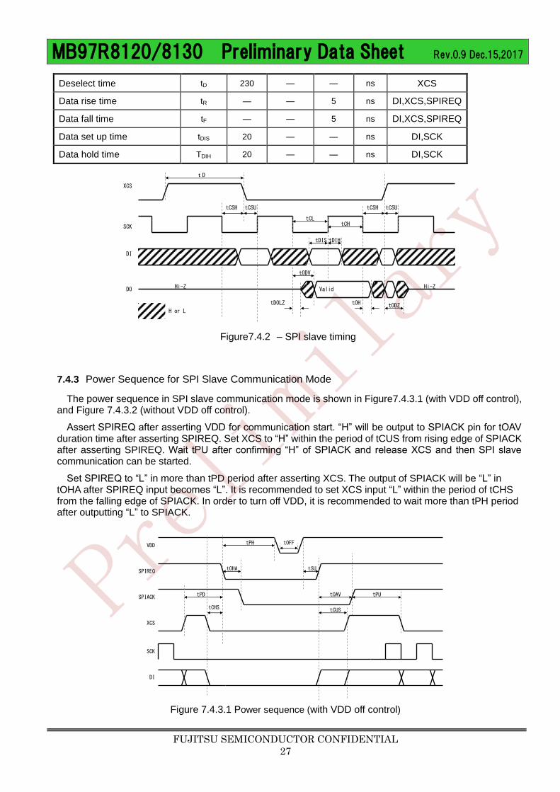
7.4.3 Power Sequence for SPI Slave Communication Mode
The power sequence in SPI slave communication mode is shown in Figure7.4.3.1 (with VDD off control), and Figure 7.4.3.2 (without VDD off control).
Assert SPIREQ after asserting VDD for communication start. “H” will be output to SPIACK pin for tOAV duration time after asserting SPIREQ. Set XCS to “H” within the period of tCUS from rising edge of SPIACK after asserting SPIREQ. Wait tPU after confirming “H” of SPIACK and release XCS and then SPI slave communication can be started.
Set SPIREQ to “L” in more than tPD period after asserting XCS. The output of SPIACK will be “L” in tOHA after SPIREQ input becomes “L”. It is recommended to set XCS input “L” within the period of tCHS from the falling edge of SPIACK. In order to turn off VDD, it is recommended to wait more than tPH period after outputting “L” to SPIACK.
Figure 7.4.3.1 Power sequence (with VDD off control)
DO Hi-Z
tODV
Hi-Z
tD
DI
SCK
XCS
H or L
tCSH tCSUtCSH tCSU
tDIS
tCHtCL
Valid
tDOLZ tODZtOH
tDIH
SCK
SPIREQ
XCS
VDD tOFF
SPIACK tOAV tPU
tSU
tPD
tOHA
tPH
tCHS tCUS
DI
MB97R8120/8130 Preliminary Data Sheet Rev.0.9 Dec.15,2017
FUJITSU SEMICONDUCTOR CONFIDENTIAL
28
Table 7.4.3 Timing specifications during SPI slave communication
Parameter Symbol Value Unit
MIN TYP MAX
SPIREQ rising start time tSU 500 ― ― µs
SPIREQ low time tRQL 1000 ― ― µs
Power hold time tPH 0 ― ― µs
XCS level hold time at power ON tPU 10 ― ― µs
XCS level hold time at power OFF tPD 1 ― ― µs
Power off time tOFF 1000 ― ― µs
Output SPIACK definite time tOAV 1 ― 20000 µs
Output SPIACK hold time tOHA 5 ― 10000 µs
XCS setup time(start) tCUS ― ― 1 µs
XCS hold time(start) tCHS ― ― 1 µs
If the device does not operate within the specified conditions of cycle or power on/off sequence, memory data cannot be guaranteed.
Figure 7.4.3.2 Power sequence (without VDD off control)
SCK
SPIREQ
XCS
VDD
SPIACK
tOAV
tPUtPD
tOHA
tCHS tCUSH or L
DI
tRQL
MB97R8120/8130 Preliminary Data Sheet Rev.0.9 Dec.15,2017
FUJITSU SEMICONDUCTOR CONFIDENTIAL
29
8 Ordering Information
9 Others
9.1 Note items
Specifications are subject to change without notice. For further information please contact each office.
All Rights Reserved.
The contents of this document are subject to change without notice.
Customers are advised to consult with sales representatives before ordering.
The information, such as descriptions of function and application circuit examples, in this document are presented solely for the purpose of reference to show examples of operations and uses of FUJITSU SEMICONDUCTOR device; FUJITSU SEMICONDUCTOR does not warrant proper operation of the device with respect to use based on such information. When you develop equipment incorporating the device based on such information, you must assume any responsibility arising out of such use of the information. FUJITSU SEMICONDUCTOR assumes no liability for any damages whatsoever arising out of the use of the information. Any information in this document, including descriptions of function and schematic diagrams, shall not be construed as license of the use or exercise of any intellectual property right, such as patent right or copyright, or any other right of FUJITSU SEMICONDUCTOR or any third party or does FUJITSU SEMICONDUCTOR warrant non-infringement of any third-party's intellectual property right or other right by using such information. FUJITSU SEMICONDUCTOR assumes no liability for any infringement of the intellectual property rights or other rights of third parties which would result from the use of information contained herein. The products described in this document are designed, developed and manufactured as contemplated for general use, including without limitation, ordinary industrial use, general office use, personal use, and household use, but are not designed, developed and manufactured as contemplated (1) for use accompanying fatal risks or dangers that, unless extremely high safety is secured, could have a serious effect to the public, and could lead directly to death, personal injury, severe physical damage or other loss (i.e., nuclear reaction control in nuclear facility, aircraft flight control, air traffic control, mass transport control, medical life support system, missile launch control in weapon system), or (2) for use requiring extremely high reliability (i.e., submersible repeater and artificial satellite).
Please note that FUJITSU SEMICONDUCTOR will not be liable against you and/or any third party for any claims or damages arising in connection with above-mentioned uses of the products.
Any semiconductor devices have an inherent chance of failure. You must protect against injury, damage or loss from such failures by incorporating safety design measures into your facility and equipment such as redundancy, fire protection, and prevention of overcurrent levels and other abnormal operating conditions.
Exportation/release of any products described in this document may require necessary procedures in accordance with the regulations of the Foreign Exchange and Foreign Trade Control Law of Japan and/or US export control laws.
The company names and brand names herein are the trademarks or registered trademarks of their respective owners.
Part Number Interface Shipping Method Wafer thickness