November, 2018 − Rev. 111 Publication Order Number:
ASX340AT/D
ASX340AT
1/4‐inch Color CMOSNTSC/PAL Digital ImageSOC with Overlay Processor
General DescriptionThe ON Semiconductor ASX340AT is a VGA-format, single-chip
CMOS active-pixel digital image sensor for automotive applications.It captures high-quality color images at VGA resolution and outputsNTSC or PAL interlaced composite video.
The VGA CMOS image sensor features ON Semiconductor’sbreakthrough low-noise imaging technology that achieves superiorimage quality (based on signal-to-noise ratio and low-light sensitivity)while maintaining the inherent size, cost, low power, and integrationadvantages of ON Semiconductor’s advanced active pixel CMOSprocess technology.
The ASX340AT is a complete camera-on-a-chip. It incorporatessophisticated camera functions on-chip and is programmable througha simple two-wire serial interface or by an attached SPI EEPROM orFlash memory that contains setup information that may be loadedautomatically at startup.
The ASX340AT performs sophisticated processing functionsincluding color recovery, color correction, sharpening, programmablegamma correction, auto black reference clamping, auto exposure,50Hz/60Hz flicker detection and avoidance, lens shading correction,auto white balance (AWB), and on-the-fly defect identification andcorrection.
The ASX340AT outputs interlaced-scan images at 60 or 50 fieldsper second, supporting both NTSC and PAL video formats. The imagedata can be output on one or two output ports:• Composite analog video (single-ended and differential
output support)• Parallel 8-, 10-bit digital
Features• Low-Power CMOS Image Sensor with Integrated Image Flow
Processor (IFP) and Video Encoder• 1/4-inch Optical Format, VGA Resolution (640 H x 480 V)
• 2x Upscaling Zoom and Pan Control
• ±40 Additional Columns and ±36 Additional Rows to Compensatefor Lens Alignment Tolerances
• Option to Use Single 2.8 V Power Supply with Off-Chip BypassTransistor
• Overlay Generator for Dynamic Bitmap Overlay
• Integrated Video Encoder for NTSC/PAL with Overlay Capabilityand 10-bit I-DAC
• Integrated Microcontroller for Flexibility
• On-Chip Image Flow Processor Performs Sophisticated Processing,Such as Color Recovery and Correction, Sharpening, Gamma, LensShading Correction, On-the-Fly Defect Correction, Auto WhiteBalancing, and Auto Exposure
www.onsemi.com
See detailed ordering and shipping information on page 3 ofthis data sheet.
ORDERING INFORMATION
IBGA63 7.5 � 7.5CASE 503AE
• Auto Black-Level Calibration• 10-Bit, On-Chip Analog-to-Digital
Converter (ADC)• Internal Master Clock Generated by
On-Chip Phase-Locked Loop (PLL)• Two-Wire Serial Programming Interface• Interface to Low-Cost EEPROM and Flash
through SPI Bus• High-Level Host Command Interface• Stand-Alone Operation Support• Comprehensive Tool Support for Overlay
Generation and Lens Correction Setup• Development System with DevWare
Applications• Automotive Rear View Camera and Side
Pixel Size and Type 5.6 �m x 5.6 �m active pinned-photodiode with high-sensitivity mode for low-light condi-tions
Sensor Clear Pixels 728 H x 560 V (includes VGA active pixels, demosaic and lens alignment pixels)
NTSC Output 720 H x 487 V
PAL Output 720 H x 576 V
Optical Area (Clear Pixels) 4.077 mm x 3.136 mm
Optical Format 1/4-inch
Frame Rate 50/60 fields/sec
Sensor Scan Mode Progressive scan
Color Filter Array RGB standard Bayer
Chief Ray Angle (CRA) 0°
Shutter Type Electronic rolling shutter (ERS)
Automatic Functions Exposure, white balance, black level offset correction, flicker detection and avoidance,color saturation control, on the-fly defect correction, aperture correction
Programmable Controls Exposure, white balance, horizontal and vertical blanking, color, sharpness, gamma cor-rection, lens shading correction, horizontal and vertical image flip, zoom, windowing,sampling rates, GPIO control
Overlay Support Utilizes SPI interface to load overlay data from external flash/EEPROM memory with thefollowing features:− Available in Analog output and BT656 Digital output− Overlay Size 360 x 480 pixel rendered into 720 x 480 (NTSC) or 720 x 576 (PAL)− Up to four (4) overlays may be blended simultaneously− Selectable readout: Rotating order user-selected− Dynamic scenes by loading pre-rendered frames from external memory− Palette of 32 colors out of 64 000− 8 colors per bitmap− Blend factor dynamically-programmable for smooth transitions− Fast update rate of up to 30 fps− Every bitmap object has independent x/y position− Statistic Engine to calibrate optical alignment− Number Generator
Windowing Programmable to any size
Analog Gain Range 0.5–16x
ADC 10-bit, on-chip
Output Interface Analog composite video out, single-ended or differential; 8-, 10-bit parallel digital output
Output Data Formats1 Digital: Raw Bayer 8-,10-bit, CCIR656, 565RGB, 555RGB, 444RGB
Data Rate Parallel: 27 MHz Pixel clock
NTSC: 60 fields/sec
PAL: 50 fields/sec
Control Interface Two-wire I/F for register interface plus high-level command exchange. SPI port to inter-face to external memory to load overlay data, register settings, or firmware extensions.
Core: 1.8 V + 5% (2.8 V + 5% power supply with off-chip bypass transistor generates a1.70 − 1.95 V core voltage supply, which is acceptable for performance.)
Supply Voltage IO: 2.8 V + 5%
Power Consumption Analog Output Only Full resolution at 60 fps: 291 mW
Digital Output Only Full resolution at 60 fps: 192 mW
See the ON Semiconductor Device Nomenclature document(TND310/D) for a full description of the naming convention used forimage sensors. For reference documentation, including information onevaluation kits, please visit our web site at www.onsemi.com.
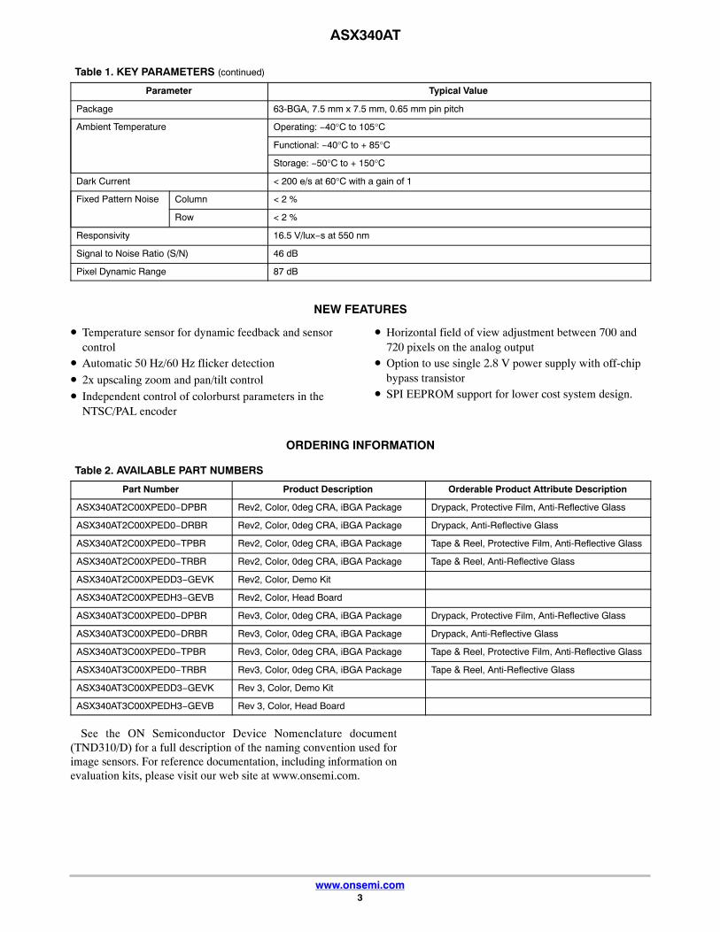
System Block DiagramThe system block diagram will depend on the application.
The system block diagram in Figure 1 shows allcomponents; optional peripheral components arehighlighted. Control information will be received by a
microcontroller through the automotive bus to communicatewith the ASX340AT through its two-wire serial bus.Optional components will vary by application.
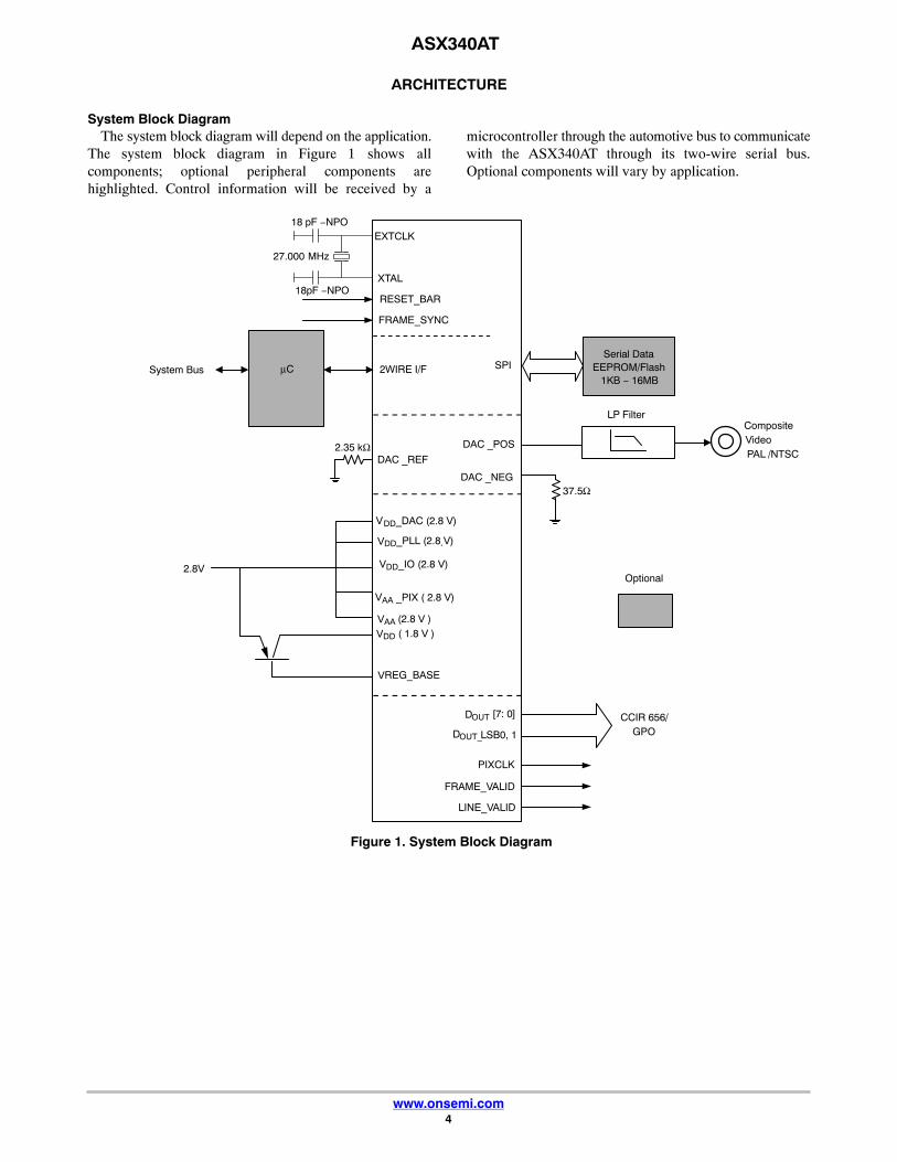
Crystal UsageAs an alternative to using an external oscillator, a
fundamental 27 MHz crystal may be connected betweenEXTCLK and XTAL. Two small loading capacitors of10–22 pF of NPO dielectric should be added as shown inFigure 3.
ON Semiconductor does not recommend using the crystaloption for applications above 85°C. A crystal oscillator withtemperature compensation is recommended.
Figure 3. Using a Crystal Instead of an External Oscillator
EXTCLK
XTAL
18 pF −NPO
27.000 MHz
Sensor
18pF −NPO
NOTE: Value of load capacitor is crystal dependent. Crystal with small load capacitor is recommended.
A2 EXTCLK Input Master input clock (27 MHz): This can either be a square-wave generated from anoscillator (in which case the XTAL input must be left unconnected) or connecteddirectly to a crystal
B1 XTAL Output If EXTCLK is connected to one pin of a crystal, this signal is connected to theother pin; otherwise this signal must be left unconnected
D2 RESET_BAR Input Asynchronous active-low reset: When asserted, the device will return all interfaces to their reset state. When released, the device will initiate the boot sequence. This signal has an internal pull-up resistor
E1 FRAME_SYNC Input This input can be used to set the output timing of the ASX340AT to a fixed point inthe frame.The input buffer associated with this input is permanently enabled. This signalmust be connected to GND if not used
REGISTER INTERFACE
F1 SCLK Input These two signals implement the serial communications protocol for access to theinternal registers and variables.F2 SDATA Input/Output
E2 SADDR Input This signal controls the device ID that will respond to serial communication commands.Two-wire serial interface device ID selection:0: 0x901: 0xBA
SPI INTERFACE
D4 SPI_SCLK Output Clock output for interfacing to an external SPI memory such as Flash/EEPROM.Tri-state when RESET_BAR is asserted
E4 SPI_SDI Input Data in from SPI device. This signal has an internal pull-up resistor
H3 SPI_SDO Output Data out to SPI device. Tri-state when RESET_BAR is asserted
H2 SPI_CS_N Output Chip selects to SPI device. Tri-state when RESET_BAR is asserted
(PARALLEL) PIXEL DATA OUTPUT
F7 FRAME_VALID Input/Output Pixel data from the ASX340AT can be routed out on this interface and processedexternally.To save power, these signals are driven to a constant logic level unless the paral-lel pixel data output or alternate (GPIO) function is enabled for these pins.This interface is disabled by default.The slew rate of these outputs is programmable.These signals can also be used as general purpose input/outputs
G7 LINE_VALID Input/Output
E6 PIXCLK Output
F8, D6, D7, C6,C7, B6, B7, A6
DOUT[7:0] Output
B3 DOUT_LSB1 Input/Output When the sensor core is running in bypass mode, it will generate 10 bits of outputdata per pixel. These two pins make the two LSB of pixel data available external-ly. Leave DOUT_LSB1and DOUT_LSB0 unconnected if not used. To save power,these signals are driven to a constant logic level unless the sensor core is runningin bypass mode or the alternate function is enabled for these pins. The slew rateof these outputs is programmable
C2 DOUT_LSB0 Input/Output
COMPOSITE VIDEO OUTPUT
F5 DAC_POS Output Positive video DAC output in differential mode.Video DAC output in single-ended mode. This interface is enabled by default us-ing NTSC/PAL signaling. For applications where composite video output is notrequired, the video DAC can be placed in a power-down state under softwarecontrol
G5 DAC_NEG Output Negative video DAC output in differential mode
A4 DAC_REF Output External reference resistor for the video DAC
MANUFACTURING TEST INTERFACE
D3 TDI Input JTAG Test pin (Reserved for Test Mode)
G2 TDO Output JTAG Test pin (Reserved for Test Mode)
F3 TMS Input JTAG Test pin (Reserved for Test Mode)
C3 TCK Input JTAG Test pin (Reserved for Test Mode)
G4 VREG_BASE Supply Voltage regulator control. Leave floating if not used
A5, A7, D8, E7,G1, G3
VDD Supply Supply for VDD core: 1.8 V nominal. Can be connected to the output of the transistor of the off-chip bypass transistor or an external 1.8 V power supply
B2, B8, C8, E3,E8, G8, H8
VDD_IO Supply Supply for digital IOs: 2.8 V nominal
H5 VDD_DAC Supply Supply for video DAC: 2.8 V nominal
A8 VDD_PLL Supply Supply for PLL: 2.8 V nominal
B4, H6 VAA Supply Analog power: 2.8 V nominal
H7 VAA_PIX Supply Analog pixel array power: 2.8 V nominal. Must be at same voltage potential asVAA
Pin AssignmentsPin 1 is not populated with a ball. That allows the device
to be identified by an additional marking.
Table 4. PIN ASSIGNMENTS
1 2 3 4 5 6 7 8
A EXTCLK GPIO13 DAC_REF VDD DOUT0 VDD VDD_PLL
B XTAL VDD_IO DOUT_LSB1 VAA GND DOUT2 DOUT1 VDD_IO
C GPIO12 DOUT_LSB0 TCK TRST_N GND DOUT4 DOUT3 VDD_IO
D GND RESET_BAR TDI SPI_SCLK GND DOUT6 DOUT5 VDD
E FRAME_SYNC SADDR VDD_IO SPI_SDI AGND PIXCLK VDD VDD_IO
F SCLK SDATA TMS AGND DAC_POS ATEST2 FRAME_VALID DOUT7
G VDD TDO VDD VREG_BASE DAC_NEG ATEST1 LINE_VALID VDD_IO
H GND SPI_CS_N SPI_SDO Reserved VDD_DAC VAA VAA_PIX VDD_IO
Table 5. RESET/DEFAULT STATE OF INTERFACES
Name Reset State Default State Notes
EXTCLK Clock running orstopped
Clock running Input
XTAL N/A N/A Input
RESET_BAR Asserted De-asserted Input
SCLK N/A N/A Input. Must always be driven to high viaa pull-up resistor in the range of 1.5 to 4.7 kΩ
SDATA High impedance High impedance Input/Output. Must always be driven to high viaa pull-up resistor in the range of 1.5 to 4.7 kΩ
SADDR N/A N/A Input. Must be permanently tied to VDD_IO or GND
SPI_SCLK High impedance Driven, logic 0 Output. Output enable is R0x0032[13]
SPI_SDI Internal pull-upenabled
Internal pull-upenabled
Input. Internal pull-up is permanently enabled
SPI_SDO High impedance Driven, logic 0 Output enable is R0x0032[13]
SPI_CS_N High impedance Driven, logic 1 Output enable is R0x0032[13]
FRAME_VALID High impedance High impedance Input/Output. This interface is disabled by default. Input buffers(used for GPIO function) powered down by default, so these pinscan be left unconnected (floating). After reset, these pins arepowered up, sampled, then powered down again as part of theauto-configuration mechanism. See Note 2LINE_VALID
PIXCLK High impedance Driven, logic 0 Output. This interface disabled by default.See Note 1DOUT7
Table 5. RESET/DEFAULT STATE OF INTERFACES (continued)
Name NotesDefault StateReset State
DOUT_LSB1 High impedance High impedance Input/Output. This interface disabled by default. Input buffers(used for GPIO function) powered down by default, so these pinscan be left unconnected (floating). After reset, these pins arepowered-up, sampled, then powered down again as part of theauto-configuration mechanismDOUT_LSB0 High impedance High impedance
DAC_POS High impedance Driven Output. Interface disabled by hardware reset and enabled bydefault when the device starts streaming
DAC_NEG
DAC_REF
TDI Internal pull-upenabled
Internal pull-upenabled
Input. Internal pull-up means that this pin can be left unconnected (floating)
TDO High impedance High impedance Output. Driven only during appropriate parts of the JTAG shiftersequence
TMS Internal pull-upenabled
Internal pull-upenabled
Input. Internal pull-up means that this pin can be left unconnected (floating)
TCK Internal pull-upenabled
Internal pull-upenabled
Input. Internal pull-up means that this pin can be left unconnected (floating)
TRST_N N/A N/A Input. Must always be driven to a valid logic level. Must be drivento GND for normal operation
FRAME_SYNC N/A N/A Input. Must always be driven to a valid logic level. Must be drivento GND if not used
GPIO12 High impedance High impedance Input/Output. This interface disabled by default. Input buffers(used for GPIO function) powered down by default, so these pinscan be left unconnected (floating)
GPIO13 High impedance High impedance Input/Output. This interface disabled by default. Input buffers(used for GPIO function) powered down by default, so these pinscan be left unconnected (floating)
ATEST1 N/A N/A Must be driven to GND for normal operation
ATEST2 N/A N/A Must be driven to GND for normal operation
1. The reason for defining the default state as logic 0 rather than high impedance is this: when wired in a system (for example, onON Semiconductor’s demo boards), these outputs will be connected, and the inputs to which they are connected will want to see a valid logiclevel. No current drain should result from driving these to a valid logic level (unless there is a pull-up at the system level).
2. These pads have their input circuitry powered down, but they are not output-enabled. Therefore, they can be left floating but they will notdrive a valid logic level to an attached device.
Sensor CoreThe sensor consists of a pixel array, an analog readout
chain, a 10-bit ADC with programmable gain and blackoffset, and timing and control as illustrated in Figure 4.
Communication
10−Bit Datato IFP
Clock
Control Register
Analog Processing
Array Timing and Control
ADC
Figure 4. Sensor Core Block Diagram
Busto IFP
SyncSignals
Active PixelSensor (APS)
Pixel Array Structure:The sensor core pixel array is configured as 728 columns
by 560 rows, as shown in Figure 5.
Figure 5. Pixel Array Description
demosaic rows
demosaic rows
dem
osai
c co
lum
ns
dem
osai
c co
lum
ns
Active pixel array640 x 480
(not to scale)
Pixel logical address = (727, 559)
Pixel logical address = (0, 0)lens alignment rows
lens alignment rows
lens
alig
nmen
t col
umns
lens
alig
nmen
t col
umns
(0, 0)(40, 36)
(687, 523)
Black rows used internally for automatic black leveladjustment are not addressed by default, but can be read outin raw output mode via a register setting.
There are 728 columns by 560 rows of optically-activepixels (that is, clear pixels) that include a pixel boundaryaround the VGA (640 x 480) image to avoid boundaryeffects during color interpolation and correction. Among the728 columns by 560 rows of clear pixels, there are 36 lens
alignment rows on the top and bottom, and 40 lens alignmentcolumns on the left and right; and there are 4 demosaic rowsand 4 demosaic columns on each side.
Figure 6 illustrates the process of capturing the image.The original scene is flipped and mirrored by the sensoroptics. Sensor readout starts at the lower right corner. Theimage is presented in true orientation by the output display.
Test PatternsDuring normal operation of the ASX340AT, a stream of
raw image data from the sensor core is continuously fed intothe color pipeline. For test purposes, this stream can bereplaced with a fixed image generated by a special testmodule in the pipeline. The module provides a selection oftest patterns sufficient for basic testing of the pipeline.
NTSC/PAL Test Pattern GenerationThere is a built-in standard EIA (NTSC) and EBU (PAL)
color bars to support hue and color saturationcharacterization. Each pattern consists of seven color bars(white, yellow, cyan, green, magenta, red, and blue). The Y,Cb and Cr values for each bar are detailed in Tables 6 and 7.
Figure 10. Color Bars
Table 6. EIA COLOR BARS (NTSC)
Nominal Range White Yellow Cyan Green Magenta Red Blue
Y 16 to 235 180 162 131 112 84 65 35
Cb 16 to 240 128 44 156 72 184 100 212
Cr 16 to 240 128 142 44 58 198 212 114
Table 7. EBU COLOR BARS (PAL)
Nominal Range White Yellow Cyan Green Magenta Red Blue
Y 16 to 235 235 162 131 112 84 65 35
Cb 16 to 240 128 44 156 72 184 100 212
Cr 16 to 240 128 142 44 58 198 212 114
CCIR-656 FormatThe color bar data is encoded in 656 data streams. The
duration of the blanking and active video periods of thegenerated 656 data are summarized in Tables 8 and 9.
Black Level Subtraction and Digital GainImage stream processing starts with black level
subtraction and multiplication of all pixel values by aprogrammable digital gain. Both operations can beindependently set to separate values for each color channel(R, Gr., Gb, B). Independent color channel digital gain canbe adjusted with registers. Independent color channel blacklevel adjustments can also be made. If the black levelsubtraction produces a negative result for a particular pixel,the value of this pixel is set to 0.
Positional Gain Adjustments (PGA)Lenses tend to produce images whose brightness is
significantly attenuated near the edges. There are also otherfactors causing fixed pattern signal gradients in imagescaptured by image sensors. The cumulative result of all thesefactors is known as image shading. The ASX340AT has anembedded shading correction module that can beprogrammed to counter the shading effects on eachindividual R, Gb, Gr., and B color signal.
The Correction FunctionThe correction functions can then be applied to each pixel
value to equalize the response across the image as follows:
where P is the pixel values and f is the color dependentcorrection functions for each color channel.
Color InterpolationIn the raw data stream fed by the sensor core to the IFP,
each pixel is represented by a 10-bit integer number, whichcan be considered proportional to the pixel’s response to aone-color light stimulus, red, green, or blue, depending onthe pixel’s position under the color filter array. Initial dataprocessing steps, up to and including the defect correction,
preserve the one-color-per-pixel nature of the data stream,but after the defect correction it must be converted to athree-colors-per-pixel stream appropriate for standard colorprocessing. The conversion is done by an edge-sensitivecolor interpolation module. The module pads the incompletecolor information available for each pixel with informationextracted from an appropriate set of neighboring pixels. Thealgorithm used to select this set and extract the informationseeks the best compromise between preserving edges andfiltering out high frequency noise in flat field areas. Theedge threshold can be set through register settings.
Color Correction and Aperture CorrectionTo achieve good color fidelity of the IFP output,
interpolated RGB values of all pixels are subjected to colorcorrection. The IFP multiplies each vector of three pixelcolors by a 3 x 3 color correction matrix. The threecomponents of the resulting color vector are all sums of three10-bit numbers. Since such sums can have up to 12significant bits, the bit width of the image data stream iswidened to 12 bits per color (36 bits per pixel). The colorcorrection matrix can be either programmed by the user orautomatically selected by the auto white balance (AWB)algorithm implemented in the IFP. Color correction shouldideally produce output colors that are corrected for thespectral sensitivity and color crosstalk characteristics of theimage sensor. The optimal values of the color correctionmatrix elements depend on those sensor characteristics andon the spectrum of light incident on the sensor. The colorcorrection parameters can be adjusted through registersettings.
To increase image sharpness, a programmable 2Daperture correction (sharpening filter) is applied tocolor-corrected image data. The gain and threshold for 2Dcorrection can be defined through register settings.
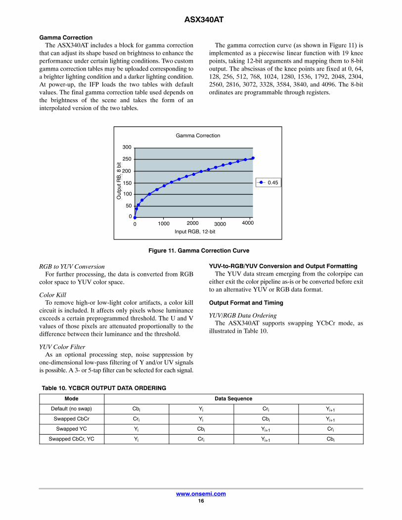
Gamma CorrectionThe ASX340AT includes a block for gamma correction
that can adjust its shape based on brightness to enhance theperformance under certain lighting conditions. Two customgamma correction tables may be uploaded corresponding toa brighter lighting condition and a darker lighting condition.At power-up, the IFP loads the two tables with defaultvalues. The final gamma correction table used depends onthe brightness of the scene and takes the form of aninterpolated version of the two tables.
The gamma correction curve (as shown in Figure 11) isimplemented as a piecewise linear function with 19 kneepoints, taking 12-bit arguments and mapping them to 8-bitoutput. The abscissas of the knee points are fixed at 0, 64,128, 256, 512, 768, 1024, 1280, 1536, 1792, 2048, 2304,2560, 2816, 3072, 3328, 3584, 3840, and 4096. The 8-bitordinates are programmable through registers.
Figure 11. Gamma Correction Curve
Input RGB, 12-bit0 1000 2000 3000 4000
0
50
100
150
200
250
300
Out
put R
B, 8
bit
0.45
Gamma Correction
RGB to YUV ConversionFor further processing, the data is converted from RGB
color space to YUV color space.
Color KillTo remove high-or low-light color artifacts, a color kill
circuit is included. It affects only pixels whose luminanceexceeds a certain preprogrammed threshold. The U and Vvalues of those pixels are attenuated proportionally to thedifference between their luminance and the threshold.
YUV Color FilterAs an optional processing step, noise suppression by
one-dimensional low-pass filtering of Y and/or UV signalsis possible. A 3- or 5-tap filter can be selected for each signal.
YUV-to-RGB/YUV Conversion and Output FormattingThe YUV data stream emerging from the colorpipe can
either exit the color pipeline as-is or be converted before exitto an alternative YUV or RGB data format.
Output Format and Timing
YUV/RGB Data OrderingThe ASX340AT supports swapping YCbCr mode, as
Uncompressed 10-Bit Bypass OutputRaw 10-bit Bayer data from the sensor core can be output
in bypass mode in two ways:• Using 8 data output signals (DOUT[7:0]) and
GPIO[1:0]. The GPIO signals are the least significant 2bits of data.
• Using only 8 signals (DOUT[7:0]) and a special 8 + 2data format, shown in Table 12.
Table 12. 2-BYTE BAYER FORMAT
Byte Bits Used Bit Sequence
Odd bytes 8 data bits D9D8D7D6D5D4D3D2
Even bytes 2 data bits + 6 unused bits 0 0 0 0 0 0 D1D0
Readout FormatsProgressive format is used for raw Bayer output.
Output Formats
ITU-R BT.656 and RGB Output:TheASX340AT can output processed video as a standard
ITU-R BT.656 (CCIR656) stream, an RGB stream, or asunprocessed Bayer data. The ITU-R BT.656 stream containsYCbCr 4:2:2 data with embedded synchronization codes.This output is typically suitable for subsequent display bystandard video equipment or JPEG/MPEG compression.
Colorpipe data (pre-lens correction and overlay) can alsobe output in YCbCr 4:2:2 and a variety of RGB formats in640 by 480 progressive format in conjunction withLINE_VALID and FRAME_VALID.
The ASX340AT can be configured to output 16-bit RGB(565RGB), 15-bit RGB (555RGB), and two types of 12-bitRGB (444RGB). Refer to Table 20 and Table 21 for details.
Bayer Output:Unprocessed Bayer data are generated when bypassing
the IFP completely−that is, by simply outputting the sensorBayer stream as usual, using FRAME_VALID,LINE_VALID, and PIXCLK to time the data. This mode iscalled sensor bypass mode.
Output Ports
Composite Video Output:The composite video output DAC is
external-resistor-programmable and supports bothsingle-ended and differential output. The DAC is driven bythe on-chip video encoder output.
Parallel Output:Parallel output uses either 8-bit or 10-bit output. Eight-bit
output is used for ITU-R BT.656 and RGB output. Ten-bitoutput is used for raw Bayer output.
Zoom SupportThe ASX340AT supports zoom x1 and x2 modes, in
interlaced and progressive scan modes. The progressivesupport is limited to the VGA at either 60 fps or 50 fps.
In the zoom x2 modes, the sensor is configured for QVGA(320 x 240), and the zoom x2 window can be configured topan around the VGA window.
FOV Stretch SupportThe ASX340AT supports the ability to control the active
“width” of the TV output line, between 692 and 720 pixels.The hardware supports two margins, each a maximum of 14pixels width, and has to be an even number of pixels.
How a camera based on the ASX340AT will beconfigured depends on what features are used. There areessentially three configuration modes for ASX340AT:
Auto-Config Mode, Flash-Config Mode, and Host-ConfigMode. Refer to System Configuration and Usage.
MULTICAMERA SUPPORT
Two or more ASX340AT sensors may be synchronized toa frame by asserting the FRAME_SYNC signal. At thatpoint, the sensor and video encoder will reset without
affecting any register settings. The ASX340AT may betriggered to be synchronized with another ASX340AT or anexternal event.
An external signal processor can take data from ITU656or raw Bayer output format and post-process or compressthe data in various formats.
Figure 13. External Signal Processing BlockDiagram
SPI
27 MHz
VIDEO_P
EXTCLK
VIDEO_N
Signal processor
1KB to 16MBEEPROM/Flash
Serial
DOUT[7:0]PIXCLK
CVBSPAL/NTSC
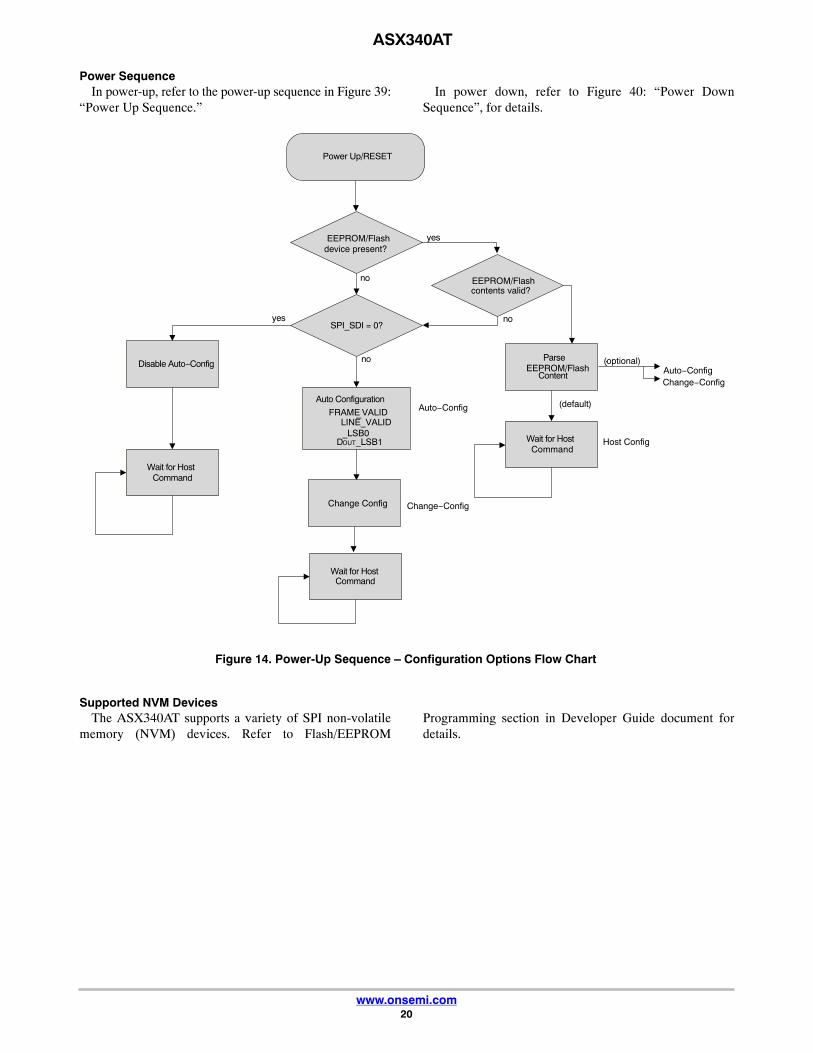
Device ConfigurationAfter power is applied and the device is out of reset by
de-asserting the RESET_BAR pin, it will enter a bootsequence to configure its operating mode. There areessentially three three configuration modes:Flash/EEPROM Config, Auto Config, and Host Config.Figure 14: “Power-Up Sequence – Configuration OptionsFlow Chart,” contains more details on the configurationoptions.
The SOC firmware supports a System Configurationphase at start-up. This consists of five modes of execution:
The System Configuration phase is entered immediatelyafter the firmware initializes following SOC power-up orreset. By default, the firmware first enters the FlashDetection mode.
The Flash Detection mode attempts to detect the presenceof an SPI Flash or EEPROM device:• If no device is detected, the firmware then samples the
SPI_SDI pin state to determine the next mode:− If SPI_SDI = 0 then it enters the Host-Config
mode− If SPI_SDI = 1 then it enters the Auto-Config
mode
• If a device is detected, the firmware switches to theFlash-Config modeIn the Flash-Config phase, the firmware interrogates the
device to determine if it contains valid configurationrecords:• If no records are detected, then the firmware enters the
Auto-Config mode• If records are detected, the firmware processes them.
By default, when all Flash records are processed thefirmware switches to the Host-Config mode. However,the records encoded into the Flash can optionally beused to instruct the firmware to proceed to one of theother mode (auto-config/change-config)
The Auto-Config mode uses the FRAME_VALID,LINE_VALID, DOUT_LSB0 and DOUT_LSB1 pins toconfigure the operation of the device, such as video formatand pedestal (refer to the Developer Guide for more details).After Auto-Config completes the firmware switches to theChange-Config mode.
In the Host-Config mode, the firmware performs noconfiguration, and remains idle waiting for configurationand commands from the host. The System Configurationphase is effectively complete and the SOC will take noactions until the host issues commands.
In the Change-Config mode, the firmware performs a“Change-Config” operation. This applies the currentconfiguration settings to the SOC, and commencesstreaming. This completes the System Configuration phase.
Host Command InterfaceON Semiconductor sensors and SOCs contain numerous
registers that are accessed through a two-wire interface withspeeds up to 400 kHz.
The ASX340AT in addition to writing or reading straightto/from registers or firmware variables, has a mechanism towrite higher level commands, the Host Command Interface(HCI). Once a command has been written through the HCI,it will be executed by on-chip firmware and the results are
reported back. In general, registers should not be accessedwith the exception of registers that are marked for “UserAccess.”
EEPROM or Flash memory is also available to storecommands for later execution. Under DMA control, acommand is written into the SOC and executed.
For a complete description of host commands, refer to theASX340AT Host Command Interface Specification.
The host issues a command by writing (through atwo-wire interface bus) to the command register. Allcommands are encoded with bit 15 set, which automaticallygenerates the host command (doorbell) interrupt to themicroprocessor.
Assuming initial conditions, the host first writes thecommand parameters (if any) to the parameters pool (in thecommand handler’s logical page), then writes the commandto command register. The firmware interrupt handler thensignals the Command Handler task to process the command.
If the host wishes to determine the outcome of thecommand, it must poll the command register waiting for thedoorbell bit to be cleared. This indicates that the firmwarecompleted processing the command. When the doorbell bitis cleared, the contents of the command register indicate thecommand’s result status. If the command generated
response parameters, the host can now retrieve these fromthe parameters pool.
NOTE: The host must not write to the parameters pool,nor issue another command, until the previouscommand completes. This is true even if thehost does not care about the result of theprevious command. Therefore, the host mustalways poll the command register to determinethe state of the doorbell bit, and ensure the bit iscleared before issuing a command.
For a complete command list and further informationconsult the Host Command Interface Specification.
An example of how (using DevWare) a command may beinitiated in the form of a “Preset” follows.
ERROR_IF= COMMAND_REGISTER, HOST_COMMAND,!=0, ”Set State command failed”,
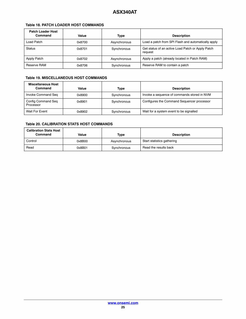
Summary of Host CommandsTable 13 through Table 18 show summaries of the host
commands. The commands are divided into the followingsections:• System Manager
• Overlay
• GPIO
• Flash Manager
• Sequencer
• Patch Loader
• Miscellaneous
• Calibration Stats
Following is a summary of the Host Interface commands.The description gives a quick orientation. The “Type”column shows if it is an asynchronous or synchronouscommand. For a complete list of all commands includingparameters, consult the Host Command InterfaceSpecification document.
Table 13. SYSTEM MANAGER COMMANDS
System Manager Host Command Value Type Description
Set State 0x8100 Synchronous Request the system enter a new state
Get State 0x8101 Synchronous Get the current state of the system
Table 14. OVERLAY HOST COMMANDS
Overlay HostCommand Value Type Description
Enable Overlay 0x8200 Synchronous Enable or disable the overlay subsystem
Get Overlay State 0x8201 Synchronous Retrieve the state of the overlay subsystem
Set Calibration 0x8202 Synchronous Set the calibration offset
Set Bitmap Property 0x8203 Synchronous Set a property of a bitmap
Get Bitmap Property 0x8204 Synchronous Get a property of a bitmap
Set String Property 0x8205 Synchronous Set a property of a character string
Load Buffer 0x8206 Asynchronous Load an overlay buffer with a bitmap (from Flash)
Load Status 0x8207 Synchronous Retrieve status of an active load buffer operation
Write Buffer 0x8208 Synchronous Write directly to an overlay buffer
Read Buffer 0x8209 Synchronous Read directly from an overlay buffer
Enable Layer 0x820A Synchronous Enable or disable an overlay layer
Get Layer Status 0x820B Synchronous Retrieve the status of an overlay layer
Set String 0x820C Synchronous Set the character string
The two-wire serial interface bus enables read/writeaccess to control and status registers within the ASX340AT.This interface is designed to be compatible with the MIPIAlliance Standard for Camera Serial Interface 2 (CSI-2) 1.0,which uses the electrical characteristics and transferprotocols of the two-wire serial interface specification.
The interface protocol uses a master/slave model in whicha master controls one or more slave devices. The sensor actsas a slave device. The master generates a clock (SCLK) thatis an input to the sensor and used to synchronize transfers.
Data is transferred between the master and the slave on abidirectional signal (SDATA). SDATA is pulled up to VDD_IOoff-chip by a pull-up resistor in the range of 1.5 to 4.7 kΩ.
ProtocolData transfers on the two-wire serial interface bus are
performed by a sequence of low-level protocol elements, asfollows:• a start or restart condition
• a slave address/data direction byte
• a 16-bit register address
• an acknowledge or a no-acknowledge bit
• data bytes
• a stop condition
The bus is idle when both SCLK and SDATA are HIGH.Control of the bus is initiated with a start condition, and thebus is released with a stop condition. Only the master cangenerate the start and stop conditions.
The SADDR pin is used to select between two differentaddresses in case of conflict with another device. If SADDR
is LOW, the slave address is 0 x 90; if SADDR is HIGH, theslave address is 0 x BA. See Table 21.
Table 21. TWO-WIRE INTERFACE ID ADDRESS SWITCHING
SADDR Two-Wire Interface Address ID
0 0x90
1 0xBA
Start ConditionA start condition is defined as a HIGH-to-LOW transition
on SDATA while SCLK is HIGH. At the end of a transfer, themaster can generate a start condition without previouslygenerating a stop condition; this is known as a “repeatedstart” or “restart” condition.
Data TransferData is transferred serially, 8 bits at a time, with the MSB
transmitted first. Each byte of data is followed by anacknowledge bit or a no-acknowledge bit. This data transfermechanism is used for the slave address/data direction byteand for message bytes.
One data bit is transferred during each SCLK clock period.SDATA can change when SCLK is low and must be stablewhile SCLK is HIGH.
Slave Address/Data Direction ByteBits [7:1] of this byte represent the device slave address
and bit [0] indicates the data transfer direction. A “0” in bit[0] indicates a write, and a “1” indicates a read. The defaultslave addresses used by the ASX340AT are 0 x 90 (writeaddress) and 0 x 91 (read address). Alternate slave addressesof 0 x BA (write address) and 0 x BB (read address) can beselected by asserting the SADDR input signal.
Message ByteMessage bytes are used for sending register addresses and
register write data to the slave device and for retrievingregister read data. The protocol used is outside the scope ofthe two-wire serial interface specification.
Acknowledge BitEach 8-bit data transfer is followed by an acknowledge bit
or a no-acknowledge bit in the SCLK clock period followingthe data transfer. The transmitter (which is the master whenwriting, or the slave when reading) releases SDATA. Thereceiver indicates an acknowledge bit by driving SDATA
LOW. As for data transfers, SDATA can change when SCLK
is LOW and must be stable while SCLK is HIGH.
No-Acknowledge BitThe no-acknowledge bit is generated when the receiver
does not drive SDATA low during the SCLK clock periodfollowing a data transfer. A no-acknowledge bit is used toterminate a read sequence.
Stop ConditionA stop condition is defined as a LOW-to-HIGH transition
on SDATA while SCLK is HIGH.
Typical OperationA typical READ or WRITE sequence begins by the
master generating a start condition on the bus. After the startcondition, the master sends the 8-bit slave address/datadirection byte. The last bit indicates whether the request isfor a READ or a WRITE, where a “0” indicates a WRITEand a “1” indicates a READ. If the address matches theaddress of the slave device, the slave device acknowledgesreceipt of the address by generating an acknowledge bit onthe bus.
If the request was a WRITE, the master then transfers the16-bit register address to which a WRITE will take place.This transfer takes place as two 8-bit sequences and the slavesends an acknowledge bit after each sequence to indicatethat the byte has been received. The master will then transferthe 16-bit data, as two 8-bit sequences and the slave sends anacknowledge bit after each sequence to indicate that the bytehas been received. The master stops writing by generating
a (re)start or stop condition. If the request was a READ, themaster sends the 8-bit write slave address/data direction byteand 16-bit register address, just as in the write request. Themaster then generates a (re)start condition and the 8-bit readslave address/data direction byte, and clocks out the registerdata, 8 bits at a time. The master generates an acknowledgebit after each 8-bit transfer. The data transfer is stoppedwhen the master sends a no-acknowledge bit.
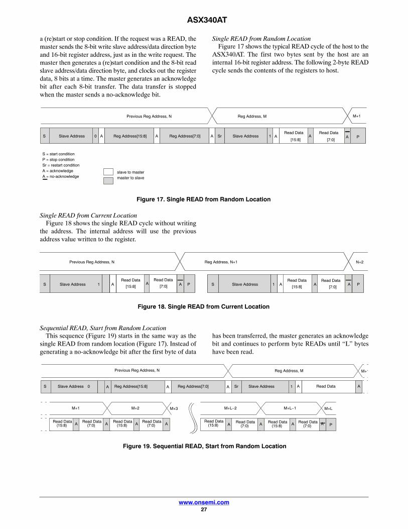
Single READ from Random LocationFigure 17 shows the typical READ cycle of the host to the
ASX340AT. The first two bytes sent by the host are aninternal 16-bit register address. The following 2-byte READcycle sends the contents of the registers to host.
Sequential READ, Start from Current LocationThis sequence (Figure 20) starts in the same way as the
single READ from current location (Figure 18). Instead ofgenerating a no-acknowledge bit after the first byte of data
has been transferred, the master generates an acknowledgebit and continues to perform byte reads until “L” bytes havebeen read.
Figure 20. Sequential READ, Start from Current Location
A
Previous Reg Address, N N+1 N+2 N+L−1 N+L
ARead DataSlave Address A1 AS PRead Data
(15:8) ARead Data
(7:0) ARead Data
(15:8)A
Read Data(7:0) A
Read Data(15:8) A
Read Data(7:0) A
Read Data
Read Data(15:8) A
Read Data(7:0)
Single Write to Random LocationFigure 21 shows the typical WRITE cycle from the host
to the ASX340AT. The first 2 bytes indicate a 16−bit address
of the internal registers with most−significant byte first. Thefollowing 2 bytes indicate the 16−bit data.
Figure 21. Single WRITE to Random Location
Slave Address 0S A Reg Address[15:8] A Reg Add ress[7:0] A P
Previous Reg Address, N Reg Address, M M+1
A
AWri te Data
Sequential WRITE, Start at Random LocationThis sequence (Figure 22) starts in the same way as the
single WRITE to random location (Figure 21). Instead ofgenerating a no-acknowledge bit after the first byte of datahas been transferred, the master generates an acknowledge
bit and continues to perform byte writes until “L” bytes havebeen written. The WRITE is terminated by the mastergenerating a stop condition.
Figure 22. Sequential WRITE, Start at Random Location
Slave Address 0S A Reg Address[15:8] A Reg Address[7:0] A Write Data
Figure 23 highlights the graphical overlay data flow oftheASX340AT. The images are separated to fit into 2 KBblocks of memory after compression.• Up to four overlays may be blended simultaneously
• Overlay size 360 x 480 pixels rendered into a displayarea of 720 x 480 pixels (NTSC) or 720 x 576 (PAL)
• Selectable readout: rotating order is user programmable
• Dynamic movement through predefined overlay images
• Palette of 32 colors out of 64,000 with eight colors perbitmap
• Blend factors may be changed dynamically to achievesmooth transitions
The host commands allow a bitmap to be writtenpiecemeal to a memory buffer through the two-wire serialinterface, and also through DMA direct from SPI Flashmemory. Multiple encoding passes may be required to fit animage into a 2 KB block of memory; alternatively, the imagecan be divided into two or more blocks to make the imagefit. Every graphic image may be positioned in the horizontaland vertical direction and overlap with other graphicimages.
The host may load an image at any time. Under control ofDMA assist, data are transferred to the off-screen buffer incompressed form. This assures that no display data arecorrupted during the replenishment of the four activeoverlay buffers.
Off-screenbuffer
Overlay buffers: 2KB each
Decompress
Blend and Overlay
Flash
Bitmaps − compressed
NOTE: These images are not actually rendered, but show conceptual objects and object blending.
To ensure a correct position of the overlay to compensatefor assembly deviation, the overlay can be adjusted withassistance from the overlay statistics engine:• The overlay statistics engine supports a windowed
8-bin luma histogram, either row-wise (vertical) orcolumn-wise (horizontal)
• The calibration statistics can be used to perform anautomatic successive-approximation search of across-hair target within the scene
• On the first frame, the firmware performs a coarsehorizontal search, followed by a coarse vertical searchin the second frame
• In subsequent frames, the firmware reduces theregion-of-interest of the search to the histogram binscontaining the greatest accumulator values, therebyrefining the search
• The resultant row and column location of the cross-hairtarget can be used to assign a calibration value to offsetselected overlay graphic image positions within theoutput image
• The calibration statistics patch also supports a manualmode, which allows the host to access the rawaccumulator values directly
Figure 25. Overlay Calibration
The position of the target will be used to determine thecalibration value that shifts the row and column position ofadjustable overlay graphics.
The overlay calibration is intended to be applied on adevice by device basis “in system,” which means after the
camera has been installed. ON Semiconductor providesbasic programming scripts that may reside in the SPI Flashmemory to assist in this effort.
In addition to the four overlay layers, a fifth layer existsfor a character generator overlay string.
There are a total of:• 16 alphanumeric characters available
• 22 characters maximum per line
• 16 x 32 pixels with 1-bit color depth
Any update to the character generator string requires thestring to be passed in its entirety with the Host Command.Character strings have their own control properties asidefrom the Overlay bitmap properties.
It can show a row of up to 22 characters of 16 x 32 pixelsresolution (32 x 32 pixels when blended with the BT 656data).
Character Generator Details
Table 23. CHARACTER GENERATOR DETAILS
Item Quantity Description
16-bit character 22 Code for one of these characters: 0, 1, 2, 3, 4, 5, 6, 7, 8, 9, /, (space), :, –, (comma), (period)
1 bpp color 1 Depth of the bit map is 1 bpp
It is the responsibility of the user to set up proper valuesin the character positioning to fit them in the same row (thatis one of the reasons that 22 is the maximum number ofcharacters).
NOTE: No error is generated if the character rowoverruns the horizontal or vertical limits of theframe.
Full Character Set for OverlayFigure 28 shows all of the characters that can be generated
by the ASX340AT.
0x0 0x4 0x8 0xC
0x1 0x5 0x9
0x2
0x3
0x6
0x7
0xA
0xB
0xD
0xE
0xF
Figure 28. Full Character Set for Overlay
MODES AND TIMING
This section provides an overview of the typical usagemodes and related timing information for the ASX340AT.
Composite Video OutputThe external pin DOUT_LSB0 can be used to configure the
device for default NTSC or PAL operation (auto-configmode). This and other video configuration settings areavailable as register settings accessible through the serialinterface.
NTSCBoth differential and single-ended connections of the full
NTSC format are supported. The differential connectionthat uses two output lines is used for low noise or longdistance applications. The single-ended connection is usedfor PCB tracks and screened cable where noise is not aconcern. The NTSC format has three black lines at thebottom of each image for padding (which most LCDs do notdisplay).
PALThe PAL format is supported with 576 active image rows.
Single-Ended and Differential Composite OutputThe composite output can be operated in a single-ended or
differential mode by simply changing the external resistorconfiguration. Refer to the Developer Guide forconfiguration options.
Parallel Output (DOUT)The DOUT[7:0] port supports both progressive and
Interlaced mode. Progressive mode (with FV and LV signal)include raw bayer(8 or 10 bit), YCbCr, RGB. Interlacedmode is CCIR656 compliant.
Figure 29 shows the data that is output on the parallel portfor CCIR656. Both NTSC and PAL formats are displayed.The blue values in Figure 29 represent NTSC (525/60). Thered values represent PAL (625/50).
Figure 29. CCIR656 8-Bit Parallel Interface Format for 525/60 (625/50) Video Systems
CO−SITED
1716 1728
Start of digital active line Next line
Figure 30 shows detailed vertical blanking informationfor NTSC timing. Table 24 for data on field, verticalblanking, EAV, and SAV states.
Figure 30. Typical CCIR656 Vertical Blanking Intervals for 525/60 Video System
Blanking
Field 1 Active Video
Blanking
Field 2 Active Video
Line 4
266
Field 1(F = 0)Odd
Field 2(F = 1)Even
EAV SAV
Line 1 (V = 1)
Line 20 (V = 0)
Line 264 (V = 1)
Line 283 (V = 0)
Line 525 (V = 0)
H = 1 H = 0
Table 24. FIELD, VERTICAL BLANKING, EAV, AND SAV STATES 525/60 VIDEO SYSTEM
Line Number F V H (EAV) H (SAV)
1–3 1 1 1 0
4–9 0 1 1 0
20–263 0 0 1 0
264–265 0 1 1 0
266–282 1 1 1 0
283–525 1 0 1 0
3. NTSC defines active video from line 20 to line 263 (corresponding to a field). This allows up to 244 active video lines in a field.4. ASX340 image output is configured to 240 lines per field; this is common practice of digital video formatting.5. When 240 lines are displayed within a field of 244 lines, the image content should start from line 22 to line 261 of the field. This ensures center
of the image and the center of the field is aligned.6. Similar consideration applies to Odd & Even fields.
Figure 31 shows detailed vertical blanking informationfor PAL timing. See Table 25 for data on field, verticalblanking, EAV, and SAV states.
Figure 31. Typical CCIR656 Vertical Blanking Intervals for 625/50 Video System
Blanking
Field 1 Active Video
Blanking
Field 2 Active Video
Field 1(F = 0)Odd
Field 2(F = 1)Even
Blanking
Line 1 (V = 1)
Line 23 (V = 0)
Line 311 (V = 1)
Line 336 (V = 0)
Line 625 (V = 1)
Line 624 (V = 1)
EAV SAVH = 1 H = 0
Table 25. Field, Vertical Blanking, EAV, and SAV States for 625/50 Video System
Line Number F V H (EAV) H (SAV)
1–22 0 1 1 0
23–310 0 0 1 0
311–312 0 1 1 0
313–335 1 1 1 0
336–623 1 0 1 0
624–625 1 1 1 0
Reset and Clocks
ResetPower-up reset is asserted or de-asserted with the
RESET_BAR pin, which is active LOW. In the reset state,all control registers are set to default values. See “DeviceConfiguration” for more details on Auto, Host, and Flashconfigurations.
Soft reset is asserted or de-asserted by the two-wire serialinterface. In soft-reset mode, the two-wire serial interfaceand the register bus are still running. All control registers arereset using default values.
ClocksThe ASX340AT has two primary clocks:
• A master clock coming from the EXTCLK signal.
• In default mode, a pixel clock (PIXCLK) running at2 × EXTCLK. In raw Bayer bypass mode, PIXCLKruns at the same frequency as EXTCLK.
When the ASX340AT operates in raw Bayer bypassmode, the image flow pipeline clocks can be shut off toconserve power.
The sensor core is a master in the system. The sensor coreframe rate defines the overall image flow pipeline framerate. Horizontal blanking and vertical blanking areinfluenced by the sensor configuration, and are also afunction of certain image flow pipeline functions. Therelationship of the primary clocks is depicted in Figure 32.
The image flow pipeline typically generates up to 16 bitsper pixel − for example, YCbCr or 565RGB − but has onlyan 8-bit port through which to communicate this pixel data.
To generate NTSC or PAL format images, the sensor corerequires a 27 MHz clock.
10 bits/pixel1 pixel/clock
16 bits/pixel1 pixel/clock
16 bits/pixel (TYP)0.5 pixel/clock
Colorpipe
Output Interface
EXTCLK Sensor Core
Sensor Pixel Clock
Sensor Master Clock
Figure 32. Primary Clock Relationships
Floating InputsThe following ASX340AT pins cannot be floated:
• SDATA–This pin is bidirectional and should not befloated
• FRAME_SYNC
• TRST_N
• SCLK
• SADDR
• ATEST1
• ATEST2
Output Data Ordering
Table 26. OUTPUT DATA ORDERING IN DOUT RGB MODE
Mode(Swap Disabled) Byte D7 D6 D5 D4 D3 D2 D1 D0
565RGBFirst R7 R6 R5 R4 R3 G7 G6 G5
Second G4 G3 G2 B7 B6 B5 B4 B3
555RGBFirst 0 R7 R6 R5 R4 R3 G7 G6
Second G5 G4 G3 B7 B6 B5 B4 B3
444xRGBFirst R7 R6 R5 R4 G7 G6 G5 G4
Second B7 B6 B5 B4 0 0 0 0
x444RGBFirst 0 0 0 0 R7 R6 R5 R4
Second G7 G6 G5 G4 B7 B6 B5 B4
7. PIXCLK is 54 MHz when EXTCLK is 27 MHz.
Table 27. OUTPUT DATA ORDERING IN SENSOR STAND−ALONE MODE
NOTE: All I/O circuitry shown above is for reference only. The actual implementation may be different.
Figure 34. NTSC Block
Pad
VDD_DAC
GND
Pad
Pad
ESDESD
DAC_REF
ESD
DAC_POS
DAC_NEG
NTSC Block
Resistor2.35 k�
Figure 35. Serial Interface
Pad
Transmitter
GND
Receiver
VDD_IO
SDATAInput/outputPad
I/O Timing
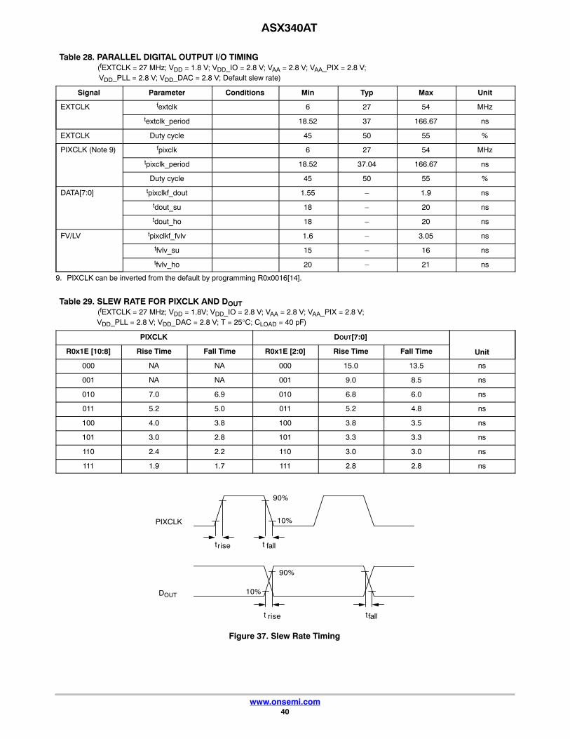
Digital OutputBy default, the ASX340AT launches pixel data, FV, and
LV synchronously with the falling edge of PIXCLK. Theexpectation is that the user captures data, FV, and LV usingthe rising edge of PIXCLK. The timing diagram is shown in.
As an option, the polarity of the PIXCLK can be invertedfrom the default by programming R0x0016[14].
1. Delay between VDD and EXTCLK depends on customer devices, i.e. Xtal, Oscillator, and so on. There is no requirement on this from thesensor.
2. Hard reset time is the minimum time required after power rails are settled. Ten clock cycles are required for the sensor itself, assuming allpower rails are settled. In a circuit where Hard reset is performed by the RC circuit, then the RC time must include the all power rail settletime and Xtal.
3. The time for Patch Config SPI or Host, that is, t5, depends on the patches being applied.
Figure 40. Power Down Sequence
VDD (1.8)
VAA (2.8)
VDD_DAC (2.8)
EXTCLK
VDD_IO (2.8)
t3
t0
t2
t1
Power Down until next Power Up Cycle
VAA_PIX
VDD_PLL
Table 32. POWER DOWN SEQUENCE
Definition Symbol Min Typical Max Unit
VDD to VDD_IO t0 0 – – �s
VDD_IO to VAA/VAA_PIX t1 0 – – �s
VAA/VAA_PIX to VDD_PLL/DAC t2 0 – – �s
Power Down until Next Power Up Time t3 100 (Note 4) – – ms
4. t3 is required between power down and next power up time, all decoupling caps from regulators must completely discharge before next powerup.
RESET_BAR HIGH to first NTSC frame tRSTH_NTSC 47 – – ms
RESET_BAR HIGH to first PAL frame tRSTH_PAL 53 – – ms
ELECTRICAL SPECIFICATIONS
Figure 45. SPI Output Timing
t su
SPI_CS_N
SPI_SCLK
SPI_SDI
SPI_SDO
tCS_SCLK
tSCLK_SDO
Table 35. SPI DATA SETUP AND HOLD TIMING
Parameter Name Conditions Min Typical Max
fSPI_SCLK SPI_SCLK Frequency 1.6875 4.5 18 MHz
tSPI_SCLK SPI_SCLK Period 55.556 592.593 ns
tsu Setup time 0.5 × tSPI_SCLK ns
tSCLK_SDO Hold time 0.5 × tSPI_SCLK + 20 ns
tCS_SCLK Delay from falling edge of SPI_CS_N torising edge of SPI_SCLK
230 ns
Table 36. ABSOLUTE MAXIMUM RATINGS
Symbol Parameter
Rating
UnitMin Max
VDD Digital power (1.8 V) −0.3 2.4 V
VDD_IO I/O power (2.8 V) −0.3 4 V
VAA VAA analog power (2.8 V) −0.3 4 V
VAA_PIX Pixel array power (2.8 v) −0.3 4 V
VDD_PLL PLL power (2.8 V) −0.3 4 V
VDD_DAC DAC power (2.8 V) −0.3 4 V
VIN DC Input Voltage −0.3 VDD_IO + 0.3 V
VOUT DC Output Voltage −0.3 VDD_IO + 0.3 V
TSTG Storage temperature −50 150 °C
Stresses exceeding those listed in the Maximum Ratings table may damage the device. If any of these limits are exceeded, device functionalityshould not be assumed, damage may occur and reliability may be affected.5. “Rating” column gives the maximum and minimum values that the device can tolerate.
Table 37. ELECTRICAL CHARACTERISTICS AND OPERATING CONDITIONS
Parameter (Note 6) Condition Min Typ Max Unit
Core digital voltage (VDD) – 1.70 1.8 1.95 V
IO digital voltage (VDD_IO) – 2.66 2.8 2.94 V
Video DAC voltage (VDD_DAC) – 2.66 2.8 2.94 V
PLL Voltage (VDD_PLL) – 2.66 2.8 2.94 V
Analog voltage (VAA) – 2.66 2.8 2.94 V
Pixel supply voltage (VAA_pix) – 2.66 2.8 2.94 V
Imager operating temperature (Note 7) – –40 +105 °C
Functional operating temperature (Note 8) –40 +85 °C
Storage temperature – –50 +150 °C
Product parametric performance is indicated in the Electrical Characteristics for the listed test conditions, unless otherwise noted. Productperformance may not be indicated by the Electrical Characteristics if operated under different conditions.6. VAA and VAA_PIX must all be at the same potential to avoid excessive current draw. Care must be taken to avoid excessive noise injection
in the analog supplies if all three supplies are tied together.7. The imager operates in this temperature range, but image quality may degrade if it operates beyond the functional operating temperature
range.8. Image quality is not guaranteed at temperatures equal to or greater than this range.
Output voltage Single-ended mode, code 000h – .021 − V
Single-ended mode, code 3FFh – 1.392 − V
Output current Single-ended mode, code 000h – 0.560 − mA
Single-ended mode, code 3FFh – 37.120 − mA
Supply current Estimate – − 25.0 mA
DAC_REF DAC Reference – 1.200 − V
R DAC_REF DAC Reference – 2.4 − K�
9. DAC_POS, DAC_NEG, and DAC_REF are loaded with resistors to simulate video output driving into a low pass filter and achieve a full outputswing of 1.4 V. Their resistor loadings may be different from the loadings in a real single-ended or differential-ended video output systemwith an actual receiving end. Please refer to the Developer Guide for proper resistor loadings.
Output voltage Differential mode, code 000h, pad dacp – .022 – V
Differential mode, code 000h, pad dacn – 1.421 – V
Differential mode, code 3FFh, pad dacp – 1.421 – V
Differential mode, code 3FFH, pad dacn – .022 – V
Output current Differential mode, code 000h, pad dacp – .587 – mA
Differential mode, code 000h, pad dacn – 37.893 – mA
Differential mode, code 3FFh, pad dacp – 37.893 – mA
Differential mode, code 3FFH, pad dacn – .587 – mA
Supply current Estimate – – 50 mA
DAC_REF DAC Reference – 1.2 V
R DAC_REF DAC Reference 2.4 KΩ
10.DAC_POS, DAC_NEG, and DAC_REF are loaded with resistors to simulate video output driving into a low pass filter and achieve a full outputswing of 1.4 V. Their resistor loadings may be different from the loadings in a real single-ended or differential-ended video output systemwith an actual receiving end. Please refer to the Developer Guide for proper resistor loadings.
Table 40. DIGITAL I/O PARAMETERS (TA = Ambient = 25°C; All supplies at 2.8 V)
Signal Parameter Definition Condition Min Typ Max Unit
AllOutputs
Load capacitance 5 – 30 pF
VOH Output high voltage 0.7 × VDD_IO – V
VOL Output low voltage – – 0.3 × VDD_IO V
IOH Output high current VOH = VDD_IO − 0.4 V 20 – 35 mA
IOL Output low current VOL = 0.4 V 29 – 53 mA
AllInputs
VIH Input high voltage 0.7 × VDD_IO – VDD_IO + 0.5 V
VIL Input low voltage –0.3 – 0.3 × VDD_IO V
IIH Input high leakage current 0.02 – 0.26 �A
IIL Input low leakage current 0.01 – 0.05 �A
Signal CAP Input signal capacitance – 6.5 – pF
11. All inputs are protected and may be active when all supplies (2.8 V and 1.8 V) are turned off.
16.This table is based on I2C standard (v2.1 January 2000).ON Semiconductor.17.Two-wire control is I2C-compatible.18.All values referred to VIHmin = 0.9 VDD and VILmax = 0.1VDD levels. Sensor EXCLK = 27 MHz.19.A device must internally provide a hold time of at least 300 ns for the SDATA signal to bridge the undefined region of the falling edge of SCLK.20.The maximum tHD;DAT has only to be met if the device does not stretch the LOW period (tLOW) of the SCLK signal.21.A Fast-mode I2C-bus device can be used in a Standard-mode I2C-bus system, but the requirement tSU;DAT 250 ns must then be met. This
will automatically be the case if the device does not stretch the LOW period of the SCLK signal. If such a device does stretch the LOW periodof the SCLK signal, it must output the next data bit to the SDATA line tr max + tSU;DAT = 1000 + 250 = 1250 ns (according to the Standard-modeI2C-bus specification) before the SCLK line is released.
Electronic versions are uncontrolled except when accessed directly from the Document Repository. Printed versions are uncontrolled except when stamped “CONTROLLED COPY” in red.
PAGE 1 OF 2
DOCUMENT NUMBER:98AON93392F
PAGE 2 OF 2
ISSUE REVISION DATE
O RELEASED FOR PRODUCTION FROM APTINA POD# ASX340 TO ON SEMICON-DUCTOR. REQ. BY D. TRUHITTE.
ON Semiconductor and are registered trademarks of Semiconductor Components Industries, LLC (SCILLC). SCILLC reserves the right to make changes without further noticeto any products herein. SCILLC makes no warranty, representation or guarantee regarding the suitability of its products for any particular purpose, nor does SCILLC assume any liabilityarising out of the application or use of any product or circuit, and specifically disclaims any and all liability, including without limitation special, consequential or incidental damages.“Typical” parameters which may be provided in SCILLC data sheets and/or specifications can and do vary in different applications and actual performance may vary over time. Alloperating parameters, including “Typicals” must be validated for each customer application by customer’s technical experts. SCILLC does not convey any license under its patent rightsnor the rights of others. SCILLC products are not designed, intended, or authorized for use as components in systems intended for surgical implant into the body, or other applicationsintended to support or sustain life, or for any other application in which the failure of the SCILLC product could create a situation where personal injury or death may occur. ShouldBuyer purchase or use SCILLC products for any such unintended or unauthorized application, Buyer shall indemnify and hold SCILLC and its officers, employees, subsidiaries, affiliates,and distributors harmless against all claims, costs, damages, and expenses, and reasonable attorney fees arising out of, directly or indirectly, any claim of personal injury or deathassociated with such unintended or unauthorized use, even if such claim alleges that SCILLC was negligent regarding the design or manufacture of the part. SCILLC is an EqualOpportunity/Affirmative Action Employer. This literature is subject to all applicable copyright laws and is not for resale in any manner.
ON Semiconductor and are trademarks of Semiconductor Components Industries, LLC dba ON Semiconductor or its subsidiaries in the United States and/or other countries.ON Semiconductor owns the rights to a number of patents, trademarks, copyrights, trade secrets, and other intellectual property. A listing of ON Semiconductor’s product/patentcoverage may be accessed at www.onsemi.com/site/pdf/Patent−Marking.pdf. ON Semiconductor reserves the right to make changes without further notice to any products herein.ON Semiconductor makes no warranty, representation or guarantee regarding the suitability of its products for any particular purpose, nor does ON Semiconductor assume any liabilityarising out of the application or use of any product or circuit, and specifically disclaims any and all liability, including without limitation special, consequential or incidental damages.Buyer is responsible for its products and applications using ON Semiconductor products, including compliance with all laws, regulations and safety requirements or standards,regardless of any support or applications information provided by ON Semiconductor. “Typical” parameters which may be provided in ON Semiconductor data sheets and/orspecifications can and do vary in different applications and actual performance may vary over time. All operating parameters, including “Typicals” must be validated for each customerapplication by customer’s technical experts. ON Semiconductor does not convey any license under its patent rights nor the rights of others. ON Semiconductor products are notdesigned, intended, or authorized for use as a critical component in life support systems or any FDA Class 3 medical devices or medical devices with a same or similar classificationin a foreign jurisdiction or any devices intended for implantation in the human body. Should Buyer purchase or use ON Semiconductor products for any such unintended or unauthorizedapplication, Buyer shall indemnify and hold ON Semiconductor and its officers, employees, subsidiaries, affiliates, and distributors harmless against all claims, costs, damages, andexpenses, and reasonable attorney fees arising out of, directly or indirectly, any claim of personal injury or death associated with such unintended or unauthorized use, even if suchclaim alleges that ON Semiconductor was negligent regarding the design or manufacture of the part. ON Semiconductor is an Equal Opportunity/Affirmative Action Employer. Thisliterature is subject to all applicable copyright laws and is not for resale in any manner.
PUBLICATION ORDERING INFORMATIONN. American Technical Support: 800−282−9855 Toll FreeUSA/Canada
Europe, Middle East and Africa Technical Support:Phone: 421 33 790 2910
LITERATURE FULFILLMENT:Literature Distribution Center for ON Semiconductor19521 E. 32nd Pkwy, Aurora, Colorado 80011 USAPhone: 303−675−2175 or 800−344−3860 Toll Free USA/CanadaFax: 303−675−2176 or 800−344−3867 Toll Free USA/CanadaEmail: [email protected]
ON Semiconductor Website: www.onsemi.com
Order Literature: http://www.onsemi.com/orderlit
For additional information, please contact your localSales Representative