University of Arkansas, Fayeeville ScholarWorks@UARK eses and Dissertations 8-2016 Asynchronous Data Processing Platforms for Energy Efficiency, Performance, and Scalability Liang Men University of Arkansas, Fayeeville Follow this and additional works at: hp://scholarworks.uark.edu/etd Part of the Digital Circuits Commons , and the VLSI and Circuits, Embedded and Hardware Systems Commons is Dissertation is brought to you for free and open access by ScholarWorks@UARK. It has been accepted for inclusion in eses and Dissertations by an authorized administrator of ScholarWorks@UARK. For more information, please contact [email protected], [email protected]. Recommended Citation Men, Liang, "Asynchronous Data Processing Platforms for Energy Efficiency, Performance, and Scalability" (2016). eses and Dissertations. 1666. hp://scholarworks.uark.edu/etd/1666
Transcript
University of Arkansas, FayettevilleScholarWorks@UARK
Theses and Dissertations
8-2016
Asynchronous Data Processing Platforms forEnergy Efficiency, Performance, and ScalabilityLiang MenUniversity of Arkansas, Fayetteville
Follow this and additional works at: http://scholarworks.uark.edu/etd
Part of the Digital Circuits Commons, and the VLSI and Circuits, Embedded and HardwareSystems Commons
This Dissertation is brought to you for free and open access by ScholarWorks@UARK. It has been accepted for inclusion in Theses and Dissertations byan authorized administrator of ScholarWorks@UARK. For more information, please contact [email protected], [email protected].
Recommended CitationMen, Liang, "Asynchronous Data Processing Platforms for Energy Efficiency, Performance, and Scalability" (2016). Theses andDissertations. 1666.http://scholarworks.uark.edu/etd/1666
As the transistor size is pushing up against physics limits in the late-Moore era, energy is
replacing performance as the top priority in circuit design considerations. The design landscape
for digital integrated circuit (IC) has changed from the one driven by performance to one driven
by energy or more-balanced goals. This shift requires next-generation circuits to be flexible and
adaptive to ever-widening application requirements. Asynchronous circuits, without global clock
as its synchronous counterpart, demonstrate distinctive resilience for the tradeoffs between energy
and performance. As highlighted in the International Technology Roadmap for Semiconductors
(ITRS), the advantages of asynchronous design include dealing with the power and thermal
bottlenecks, less electromagnetic interface (EMI), and tolerating process variations and external
voltage fluctuations in a wider region, as multibillion-transistor chips and multi-core architectures
are targeted [1]. This dissertation work is to develop and explore adaptive system architecture of
the asynchronous circuits with the following features:
1) Performance – In synchronous circuits, a fixed clock period is chosen based on the worst-case
timing between the pipeline stages. However, in asynchronous pipeline, subsystems are only
synchronized locally by the handshaking protocols between them, which are referred to as self-
timed systems [2]. The subsystem consumes the output produced by the previous subsystem
as soon as they are generated, without waiting for the global clock toggling. Therefore,
asynchronous circuits are widely accepted for the average-case performance rather than the
worst-case as in synchronous ones [3];
2) Energy efficiency – CMOS circuits have the active and static energy consumption when
2
processing data and static power consumption when they are idle. A periodic clock will force
the circuit to be active even though there is no new data for processing. Clock gating is a
common method for migrating the energy overhead caused by undesired clock toggling in the
idle mode. However, external control and observation blocks are required to manipulate the
clock, which will deteriorate the energy efficiency and performance [4]. Without the global
clock, only the subsystems that are active will dissipate power in asynchronous circuits. For
the leakage reduction, power-gating mechanism can also be implemented in asynchronous
circuits using the handshaking signals without extra control blocks as in synchronous ones;
3) Scalability. The self-timed nature of asynchronous circuit avoids the clocked related issues in
the synchronous counterpart. Each asynchronous subsystem is functional module containing
both timing and data information explicitly in the interfaces. Without global timing analysis
and clock-based sequencing [5], it is easy to compose asynchronous blocks into large systems.
1.1 Techniques for Throughput Improvement and Power Reduction
Besides the intrinsic characteristics of the asynchronous logic, advanced techniques, e.g.,
parallelism, dynamic voltage scaling (DVS), and sub-threshold operations, show more promising
results when applied to asynchronous circuits for ultra-low power applications.
1.1.1 Dynamic Voltage Scaling
DVS is the key for real-time energy optimization in adaptive systems. The active power
dissipated by a chip using static CMOS gates can be expressed as , where C is the
capacitance being switched per operation; V is the supply voltage and f is the switching frequency.
The active power consumption of the circuit can decrease quadratically as supply voltage scales
3
down. This technique was first introduced for low-power operation using self-timed circuits in [6],
with FIFO buffers inserted for state detecting and dynamic voltage scaling. An Asynchronous
Array of Simple Processors (AsAP) chip [7], designed and fabricated by the VLSI Computation
Laboratory at the University of California, Davis, is implementing a similar technology for power
reduction. In the synchronous systems, the voltage scaling range is limited to guarantee the circuit
working properly under the related timing issues. A research conducted by [8] indicates that an
18×18 multiplier at 90 MHz has an error rate of 1.3% with the energy saving of 35% when scaling
down the voltage from 1.8V to 1.38V. Adaptive Voltage Scaling (AVS) is used to control the
supply voltage for the actual requirements – when the voltage scales down, the frequency decreases
for timing closure. For chip multiprocessors (CMPs), a variation-aware technique is introduced in
[9] and several multi-core voltage-frequency island (VFI) strategies are evaluated in [10]. Panoptic
Dynamic Voltage Scaling (PDVS), a fine-gained DVS framework, is presented in [11] to use of
Local Voltage Dithering (LVD) into sub-threshold mode for additional energy savings [12].
Learning based DVS, employing a machine learning approach for temperature, performance and
energy management, is proposed in [13]. Due to the additional hardware cost and associated
control to minimize energy, synchronous systems employing DVS typically have a small set of
voltage-frequency pairs and have to mitigate the effects of process variation, thermal variation and
timing fluctuations caused by DVS itself. In [14], asynchronous data path across voltage domains
is developed for multi-rate signal processing applications. Activity detection [15] is applied to
asynchronous network-on-chip (ANOC) nodes for voltage scaling and static power reduction.
1.1.2 Throughput Improvement
Throughput refers to the rate at which new data can be input to the system, and similarly,
the rate at which new outputs appear from the system. Pipelining is commonly used in synchronous
4
circuits to improve the system throughput, with the drawback of increasing latency. In synchronous
pipelined circuits, the clock rate depends on the worst-case timing between the pipeline stages;
while in asynchronous circuits, the throughput and latency depend on the actual computing time
of each pipeline stage, which are data dependent and lead to the average case performance.
However, asynchronous pipelines usually have additional components for handshaking generation
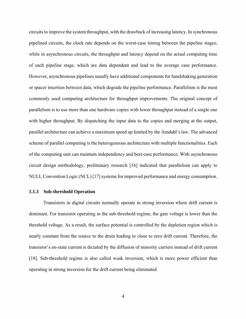
or spacer insertion between data, which degrade the pipeline performance. Parallelism is the most
commonly used computing architecture for throughput improvements. The original concept of
parallelism is to use more than one hardware copies with lower throughput instead of a single one
with higher throughput. By dispatching the input data to the copies and merging at the output,
parallel architecture can achieve a maximum speed up limited by the Amdahl’s law. The advanced
scheme of parallel computing is the heterogeneous architecture with multiple functionalities. Each
of the computing unit can maintain independency and best-case performance. With asynchronous
circuit design methodology, preliminary research [16] indicated that parallelism can apply to
NULL Convention Logic (NCL) [17] systems for improved performance and energy consumption.
1.1.3 Sub-threshold Operation
Transistors in digital circuits normally operate in strong inversion where drift current is
dominant. For transistor operating in the sub-threshold regime, the gate voltage is lower than the
threshold voltage. As a result, the surface potential is controlled by the depletion region which is
nearly constant from the source to the drain leading to close to zero drift current. Therefore, the
transistor’s on-state current is dictated by the diffusion of minority carriers instead of drift current
[18]. Sub-threshold regime is also called weak inversion, which is more power efficient than
operating in strong inversion for the drift current being eliminated.
5
Lowering down the supply voltage seems to be a straightforward way to take advantage of
the power efficiency of sub-threshold transistors. However, with the supply voltage scaling down,
the sub-threshold leakage current will increase significantly [19]. Compared to bulk silicon,
FDSOI (Fully Depleted Silicon-On-Insulator) provides up to 90% [20] lower junction leakage and
full dielectric isolation of the transistor, making it suitable for low power CMOS applications.
Combining the advantages of FDSOI with transistors optimized for sub-threshold operation, the
dynamic power and leakage power are reduced while maintaining the performance of digital
systems.
1.2 Proposed Research and Approach
The proposed research is to develop a design methodology and platform utilizing
asynchronous logic for designing digital signal processing unit capable of achieving the optimal
energy-performance tradeoff in dynamic operations across a wide range of applications. Parallel
architecture, dynamic voltage scaling, and sub-threshold operateability, are incorporated. The
major features of the digital processors designed using the proposed methodology include:
1) Adaptive – the designed asynchronous systems are capable of adjusting the supply voltage
based on real-time workload. When input data rate is fast, the supply voltage to the core is
raised to boost performance; when input data rate is slow, the cores enter sleep mode and the
supply voltage is lowered to reduce power consumption, which could become even lower with
sub-threshold operation. While input data rate detection is not a trivial task for synchronous
systems and often requires complicated logic, it is inherent for the proposed asynchronous
systems since the handshaking signals naturally serve for this purpose;
2) Optimal energy consumption – The proposed methodology is capable of achieving optimal
6
energy consumption in the designed processors while operating in active and idle modes. The
throughput-based system status detection and workload prediction algorithm guarantee
optimal operations of the cores integrated on the platform. The dynamically adaptive scaling
based on real-time workload and system status ensures the system only consumes the amount
of active energy needed to maintain the required performance. Power gating mechanism is
incorporated in the circuit paradigm for leakage reduction in idle or near-idle mode operation.
3) Highly reliable – the proposed asynchronous system is correct-by-construction, where the
system’s outputs are always correct as long as the transistors can switch properly. Timing
variances induced by process variation, temperature change, or voltage fluctuation, which
require sophisticated timing analysis and large timing margins in synchronous systems, have
little or no impact to the functionalities of the asynchronous systems. It is especially important
for DVS to ensure no data is lost during the adjustment of system performance.
4) Large-scale heterogeneous integration – the proposed methodology can be adopted to design
asynchronous processors suitable for a large variety of applications. The number of internal
nodes can also be increased or decreased to accommodate load variation and number of inputs.
Heterogeneous scalability is enabled to use components with different functionality. Due to
the local handshaking feature of the asynchronous circuit, two data routing protocols are
developed to scale vertically or horizontally.
The design methodology is developed and utilized during the completion of the grant from
the National Science Foundation (NSF). MIT Lincoln Laboratory (MITLL) sponsored the 90nm
FDSOI tapeout for the design. The tapeout was focused on creating the components for the
homogenous platform and its adaptive control blocks.
7
1.3 Dissertation Organization
Chapter 2 provides the background information introducing the asynchronous paradigm
adapted by this work. Chapter 3 contains the design and throughput optimization approach of the
computing units in the asynchronous circuitry. Chapter 4 presents the architecture of the adaptive
homogeneous platform with Dynamic Voltage Control and load prediction algorithm. Chapter 5
presents the architecture of the heterogeneous platform that can be scaled horizontally and
vertically. Chapter 6 contains the simulation results for both the homogeneous and heterogeneous
architectures as well as the physical testing of the asynchronous circuits and the homogeneous
platform. Chapter 7 summarizes the findings and concepts discussed in this dissertation, and
examines future possibilities of this work.
8
2 Background
2.1 Asynchronous Circuits
Asynchronous circuits, or self-timed circuits, are sequential digital logic circuits without a
global clock signal. The design styles of asynchronous circuits vary from the bounded-delay model
to the delay-insensitive model. In the bounded-delay model, it assumes that given enough time, a
sub-circuit will have settled in response to an input and a new input can procedure safely [21].
Different from the bounded-delay asynchronous model, delay-insensitive circuits are correct by
construction, assuming unbounded delays in both elements and wires. However, arbitrary gate and
wire delay can exist in the circuit, which makes the timing model too restrictive to design practical
circuits [22]. Quasi-Delay-Insensitive (QDI) logic emerged in the middle of 1980s with an
assumption that the wire delays are negligible compared to gate delays. It partitions wires into
critical and non-critical paths [23, 24]. For the non-critical path, there is no timing assumption,
while in the critical wires the skew between different branches is assumed to be smaller than the
minimum gate delay. With those assumptions, QDI methodology is widely adopted by the
asynchronous community for circuit design.
2.2 NULL Convention Logic (NCL)
NULL Conventional Logic (NCL) is one of the QDI asynchronous paradigms. To achieve
delay-insensitivity, NCL circuits utilize multi-rail encoding; and the most prevalent multi-rail
scheme is dual-rail [25]. In dual-rail encoding, the two data transition wires encoded in such a way
that one more value ‘no data’ called NULL state can be transmitted in addition to the actual data
values. As shown in Table 1, the encoding is one-hot: dual-rail encoding with ‘00’ being the NULL
and ‘10’, ‘01’ corresponding to TRUE and FALSE, respectively. The other combination ‘11’ is
9
invalid in dual-rail encoding.
Table 1 Dual-Rail Encoding in NCL
DATA0 DATA1 NULL INVALID
Rail0 1 0 0 1
Rail1 0 1 0 1
NCL circuits are composed of 27 fundamental logic gates, which are named as threshold
gates. The idea of NCL threshold gates was proposed by Theseus Logic, Inc. [26]. By using
arbitrary m-of-n threshold gates with hysteresis, it reduces the implementation complexity with
QDI logic. Each gate transitions from logic0 to logic1 only when a certain threshold of asserted
inputs is achieved. The generic threshold gate is named as THmn, with m as the threshold and n
as the inputs. The output will be set high when any m inputs have gone high and be set low when
all inputs are low. So the C-element and Boolean OR gates can be seen as n-of-n and 1-of-n
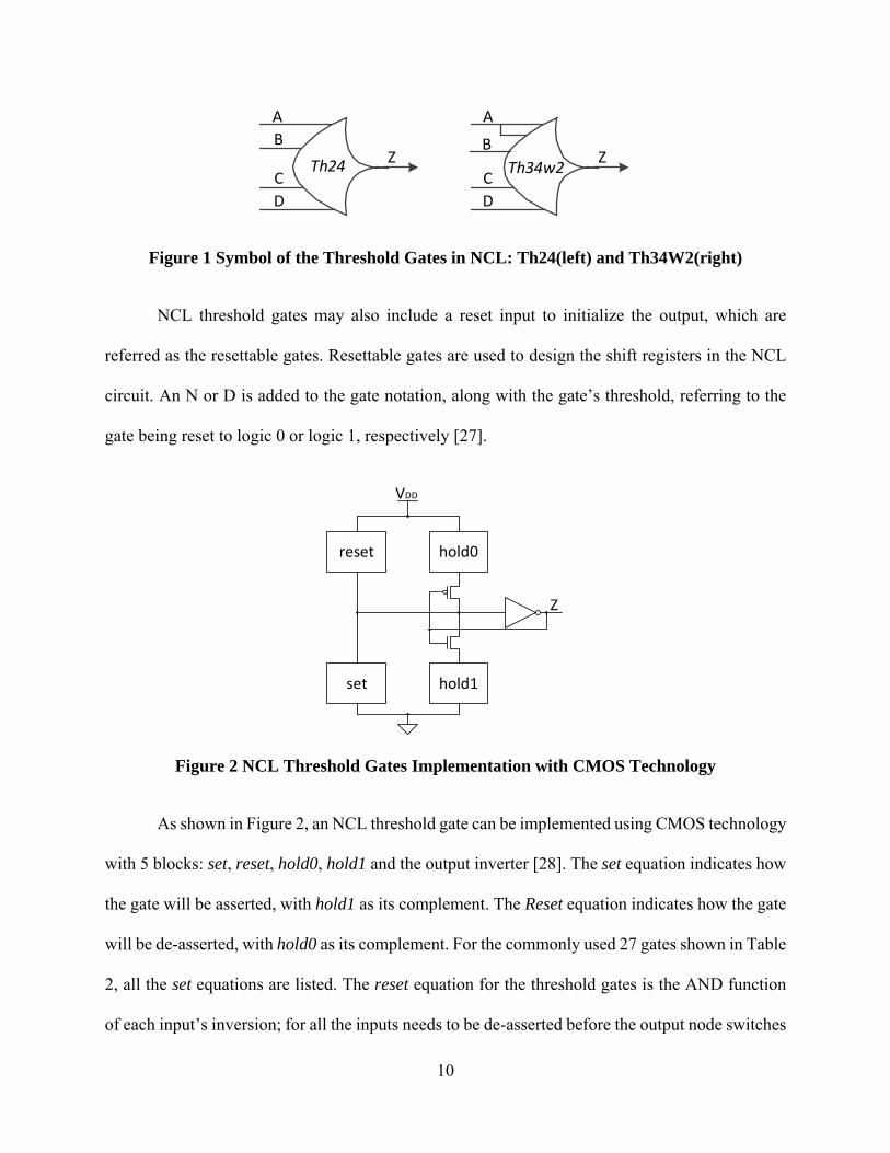
threshold gates with hysteresis. For example, a TH24 is a four-input gate that requires two or more
to be asserted before the output is asserted. The symbol for the TH24 is shown below in Figure
1(left). As a variation of the basic threshold gates, weighted threshold gates are used to indicate
special functionality, donated as THmnWw1w2…wR, where 1 < wR ≤ m. The values of w1,w2,…wR
indicate the weights of the inputs in order, i.e., w1 is the weight of the first input A, w2 is the weight
of the second input B, etc. For example, a TH34w2 is a gate with four inputs that asserts its output
when a threshold of three is achieved; due to the weighted inputs on this gate, the A input has a
weight of two, thereby only requiring one other input asserted to assert the output. The B, C and
D inputs have a weight of one, and therefore are not indicated in the list of weights. This concept
is greatly simplified by studying the symbol assigned to weighted threshold gates, as shown in
Figure 1(right).
10
Th24
A
BZ
D
CTh34w2
A
BZ
D
C
Figure 1 Symbol of the Threshold Gates in NCL: Th24(left) and Th34W2(right)
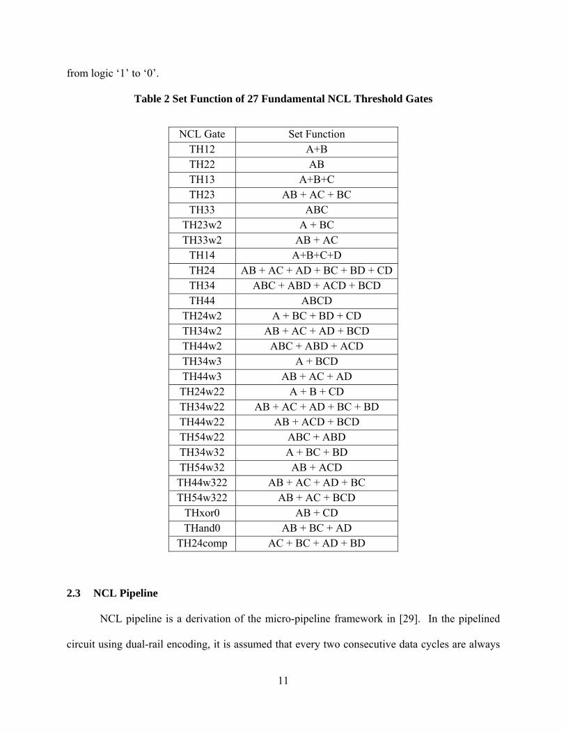
NCL threshold gates may also include a reset input to initialize the output, which are
referred as the resettable gates. Resettable gates are used to design the shift registers in the NCL
circuit. An N or D is added to the gate notation, along with the gate’s threshold, referring to the
gate being reset to logic 0 or logic 1, respectively [27].
reset hold0
set hold1
VDD
Z
Figure 2 NCL Threshold Gates Implementation with CMOS Technology
As shown in Figure 2, an NCL threshold gate can be implemented using CMOS technology
with 5 blocks: set, reset, hold0, hold1 and the output inverter [28]. The set equation indicates how
the gate will be asserted, with hold1 as its complement. The Reset equation indicates how the gate
will be de-asserted, with hold0 as its complement. For the commonly used 27 gates shown in Table
2, all the set equations are listed. The reset equation for the threshold gates is the AND function
of each input’s inversion; for all the inputs needs to be de-asserted before the output node switches
11
from logic ‘1’ to ‘0’.
Table 2 Set Function of 27 Fundamental NCL Threshold Gates
NCL Gate Set Function TH12 A+B TH22 AB TH13 A+B+C TH23 AB + AC + BC TH33 ABC
TH23w2 A + BC TH33w2 AB + AC
TH14 A+B+C+D TH24 AB + AC + AD + BC + BD + CDTH34 ABC + ABD + ACD + BCD TH44 ABCD
TH24w2 A + BC + BD + CD TH34w2 AB + AC + AD + BCD TH44w2 ABC + ABD + ACD TH34w3 A + BCD TH44w3 AB + AC + AD TH24w22 A + B + CD TH34w22 AB + AC + AD + BC + BD TH44w22 AB + ACD + BCD TH54w22 ABC + ABD TH34w32 A + BC + BD TH54w32 AB + ACD TH44w322 AB + AC + AD + BC TH54w322 AB + AC + BCD
THxor0 AB + CD THand0 AB + BC + AD
TH24comp AC + BC + AD + BD
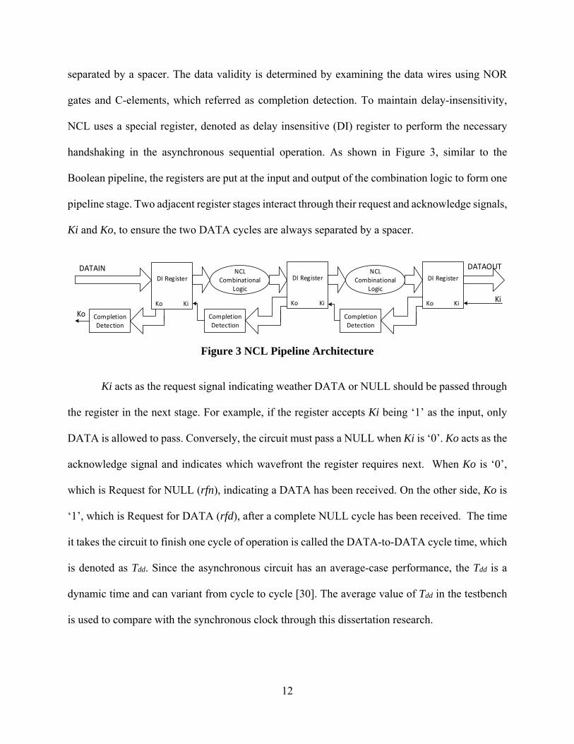
2.3 NCL Pipeline
NCL pipeline is a derivation of the micro-pipeline framework in [29]. In the pipelined
circuit using dual-rail encoding, it is assumed that every two consecutive data cycles are always
12
separated by a spacer. The data validity is determined by examining the data wires using NOR
gates and C-elements, which referred as completion detection. To maintain delay-insensitivity,
NCL uses a special register, denoted as delay insensitive (DI) register to perform the necessary
handshaking in the asynchronous sequential operation. As shown in Figure 3, similar to the
Boolean pipeline, the registers are put at the input and output of the combination logic to form one
pipeline stage. Two adjacent register stages interact through their request and acknowledge signals,
Ki and Ko, to ensure the two DATA cycles are always separated by a spacer.
DI Register
KiKo
NCL Combinational
Logic
DI Register
KiKo
Completion Detection
NCL Combinational
Logic
DI Register
KiKo
Completion Detection
Completion Detection
DATAIN DATAOUT
Ko
Ki
Figure 3 NCL Pipeline Architecture
Ki acts as the request signal indicating weather DATA or NULL should be passed through
the register in the next stage. For example, if the register accepts Ki being ‘1’ as the input, only
DATA is allowed to pass. Conversely, the circuit must pass a NULL when Ki is ‘0’. Ko acts as the
acknowledge signal and indicates which wavefront the register requires next. When Ko is ‘0’,
which is Request for NULL (rfn), indicating a DATA has been received. On the other side, Ko is
‘1’, which is Request for DATA (rfd), after a complete NULL cycle has been received. The time
it takes the circuit to finish one cycle of operation is called the DATA-to-DATA cycle time, which
is denoted as Tdd. Since the asynchronous circuit has an average-case performance, the Tdd is a
dynamic time and can variant from cycle to cycle [30]. The average value of Tdd in the testbench
is used to compare with the synchronous clock through this dissertation research.
13
Two special requirements in the NCL circuit, Input-Completeness [31] and Observability
[32], prevent the NCL circuit can be easily adopted by commercial CAD tools. Input-
Completeness requires that all outputs of a combinational circuit may not transition from NULL
to DATA or NULL to DATA before a complete input set arrives. Observability requires only the
transitions that are used to determine the output exist in the current DATA cycle. Otherwise, an
orphan [31] may propagate through a gate and cause unpredictability.
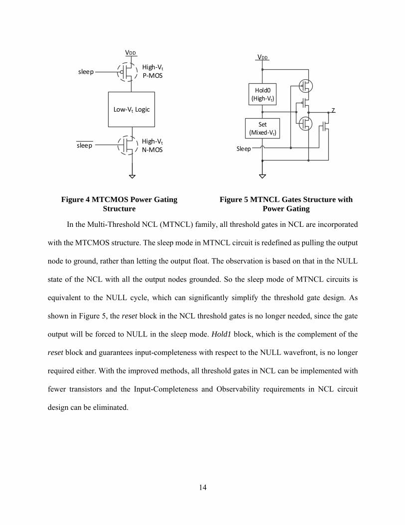
2.4 NCL with Multi-threshold CMOS Technology
Multi-threshold technology is commonly used as power-gating mechanism in the
synchronous design by utilizing transistors with different threshold voltages (Vt). Low-Vt
transistors are faster but have high leakage, whereas high-Vt transistors are slower but have far
less leakage current. In an MTCMOS circuit, the high-Vt transistors are used in the power path to
shut down the leakage when the circuit is idle; and the low-Vt transistors are used in the data path
to maintain the speed when the circuit is processing data [33]. The high-Vt transistors are
controlled by a sleep signal. As shown in Figure 4, the sleep signal is de-asserted during active
mode; the low-Vt logic will be able to process data with power and ground connected. When the
circuit is idle, the sleep signal is asserted, disconnecting power from the data processing circuit
with low-Vt transistors. However, when the data processing circuit is large, it is difficult to size
the sleep transistors for large power supply. A fine-grained architecture is developed by utilizing
NCL in conjunction with the MTCMOS technique in [34].
14
sleep
Low‐Vt Logic
High‐Vt
N‐MOS
VDD
sleep
High‐Vt
P‐MOS
Figure 4 MTCMOS Power Gating Structure
Hold0(High‐Vt)
Set(Mixed‐Vt)
VDD
Z
Sleep
Figure 5 MTNCL Gates Structure with Power Gating
In the Multi-Threshold NCL (MTNCL) family, all threshold gates in NCL are incorporated
with the MTCMOS structure. The sleep mode in MTNCL circuit is redefined as pulling the output
node to ground, rather than letting the output float. The observation is based on that in the NULL
state of the NCL with all the output nodes grounded. So the sleep mode of MTNCL circuits is
equivalent to the NULL cycle, which can significantly simplify the threshold gate design. As
shown in Figure 5, the reset block in the NCL threshold gates is no longer needed, since the gate
output will be forced to NULL in the sleep mode. Hold1 block, which is the complement of the
reset block and guarantees input-completeness with respect to the NULL wavefront, is no longer
required either. With the improved methods, all threshold gates in NCL can be implemented with
fewer transistors and the Input-Completeness and Observability requirements in NCL circuit
design can be eliminated.
15
2.5 MTNCL Pipeline
sleep
CompKo Ki
sleep
Regm
sleep
CompKo Ki
sleep
Regm
sleep
Ko
Sleepin
MTNCL Combinational Logic
sleep
CompKo Ki
sleep
Regm
sleep
Sleepout
Ki
MTNCL Combinational Logic
DATAOUTDATAIN
Figure 6 MTNCL Pipeline Architecture
The framework for the MTNCL pipeline architecture is shown in Figure 6. When all
MTNCL gates in a pipeline stage are in sleep mode, all gate outputs are forced to ground. It is
equivalent to the pipeline being in the NULL state. Early Completion Detection [35] is used to
further improve the throughput as well as maintain delay insensitivity in the pipeline architecture.
The handshaking signals Ko and Ki in the NCL pipeline can naturally serves as the sleep control
signal in the MTNCL pipeline. As shown in Figure 7, the output of the completion logic, Ko, is
used to sleep the combinational MTNCL logic for the subsequent stages as well as the DI register
and completion logic. Initially, the circuit elements in the MTNCL pipeline are in NULL state
with all the Kos in rfd. After the first DATA wavefront presents on the input ports, the completion
circuit will deassert Ko to rfn, which wakes up the subsequent register and combinational logic to
propagate the input DATA. The deasserted Ko will hold its value until following NULL wavefront
presents on the input ports and the completion logic is forced to sleep by the sleeping signal. When
Ko is asserted to rfd, the subsequent register and combinational logic will be forced to sleep, thus
generating a NULL wavefront. The DATA/NULL cycle continues repeatedly to fill all the pipeline
stages before the first valid data presents on the output ports.
16
th12m
D[0].rail0
D[0].rail1
th12m
D[1].rail0
D[1].rail1
th12m
D[n].rail0
D[n].rail1
Andtree(th44m)
th22
sleep
Ki
Ko
Figure 7 Early Completion Detection Block in MTNCL Pipeline
17
3 Digital Signal Processing Circuits Design in MTNCL
3.1 Design of the Finite Impulse Response (FIR) Filter
In digital signal processing (DSP), an FIR filter is the convolution of the input sequence
and a time-reversed copy of a known pulse-shape, which is defined as the coefficients. For a causal
discrete-time FIR filter with N taps, each value in the output sequence is the sum of the most recent
input values multiplied by the coefficients, as shown in equation (1):
1 ∑ (1)
where:
is the input signal;
is the output signal;
is the filter order; a Nth-order filter has (N+1) terms on the right-hand side;
is the coefficient of the impulse response at the ith instant of a Nth-order FIR filter.
For the hardware implementation, an FIR filter can be built with three digital elements, i.e., a
unit delay component, a multiplier, and an adder. The unit delay updates its output once per sample
period, using the value of the input as its new output value. By cascading a set of delay units to
form a delay chain, the input sequence , 1 , … 1 can be accessed. The output
sequence on the delay line is scaled by the coefficients, which are constants in most DSP
applications for the multiply operation. Figure 8 shows a conventional tapped delay line realization
of an FIR filter in synchronous logic.
18
DFFX(n)
× × ×
+ +
×
+Y(n)
DFF DFF
C0 C1 C2 Cn
Figure 8 Conventional FIR Filter with Tapped Delay Line
3.1.1 Generic Ripple Carry Adder Design in MTNCL
The combinational logic of the ripple carry adder is a serial connection of the full adders.
The MTNCL registers are inserted at the input and output ports of the combinational logic to form
the generic design. The Sum of Product (SOP) of the full adder in NCL can be presented by the
equation shown in equation (2), with X and Y as the single bit input and the CIN as the carry in bit.
The sum S and carry out COUT are mapped to the output of TH23 and TH34w2 gates in MTNCL.
To separate form the NCL gates, suffix ‘m’ is used in the MTNCL gates, as shown in Figure 9.
(2)
19
th23m
X.rail0
th34w2m
Y.rail0
CIN.rail0
X.rail1Y.rail1CIN.rail1
COUT.rail0
S.rail1
th23m
X.rail1
th34w2m
Y.rail1
CIN.rail1
X.rail0
Y.rail0CIN.rail0
COUT.rail1
S.rail0
sleep
sleep
Figure 9 Full Adder Implementation with MTNCL Gates
sleep
Comp1
sleep
Regm1
sleep
Comp2
sleep
Regm2
sleep
Ko
Sleepin
Ripple Carry Adder(comb)
Sleepout
Ki
PX&Y
Kor1
Buffer for the sleep signal
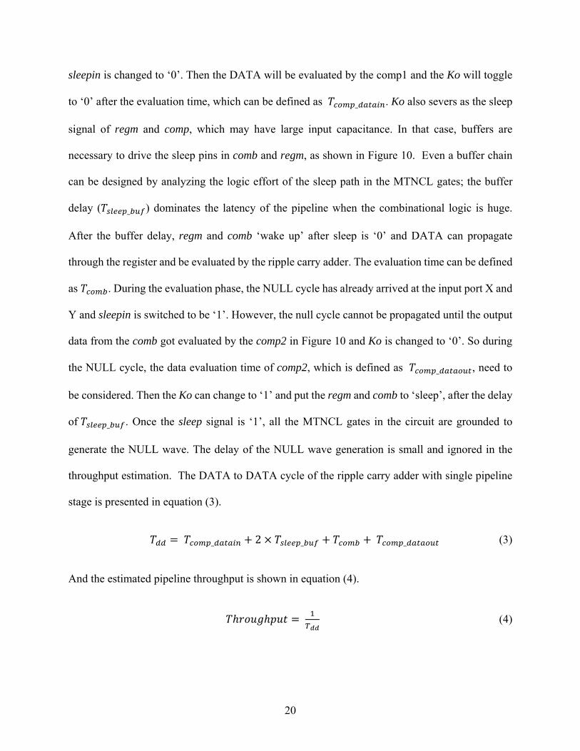
Figure 10 Ripple Carry Adder in MTNCL
Figure 10 shows the ripple carry adder with single pipeline stage. The register (regm) and
completion detection block (comp) are placed at the input and output of the combination logic
(comb). Initially, all the handshaking signals are ‘1’ and the internal data path are in NULL state.
Since Ko is ‘1’ and is requesting for data (rfd), a DATA cycle appears on the input path and the
20
sleepin is changed to ‘0’. Then the DATA will be evaluated by the comp1 and the Ko will toggle
to ‘0’ after the evaluation time, which can be defined as _ . Ko also severs as the sleep
signal of regm and comp, which may have large input capacitance. In that case, buffers are
necessary to drive the sleep pins in comb and regm, as shown in Figure 10. Even a buffer chain
can be designed by analyzing the logic effort of the sleep path in the MTNCL gates; the buffer
delay ( _ ) dominates the latency of the pipeline when the combinational logic is huge.
After the buffer delay, regm and comb ‘wake up’ after sleep is ‘0’ and DATA can propagate
through the register and be evaluated by the ripple carry adder. The evaluation time can be defined
as . During the evaluation phase, the NULL cycle has already arrived at the input port X and
Y and sleepin is switched to be ‘1’. However, the null cycle cannot be propagated until the output
data from the comb got evaluated by the comp2 in Figure 10 and Ko is changed to ‘0’. So during
the NULL cycle, the data evaluation time of comp2, which is defined as _ , need to
be considered. Then the Ko can change to ‘1’ and put the regm and comb to ‘sleep’, after the delay
of _ . Once the sleep signal is ‘1’, all the MTNCL gates in the circuit are grounded to
generate the NULL wave. The delay of the NULL wave generation is small and ignored in the
throughput estimation. The DATA to DATA cycle of the ripple carry adder with single pipeline
stage is presented in equation (3).
_ 2 _ _ (3)
And the estimated pipeline throughput is shown in equation (4).
(4)
21
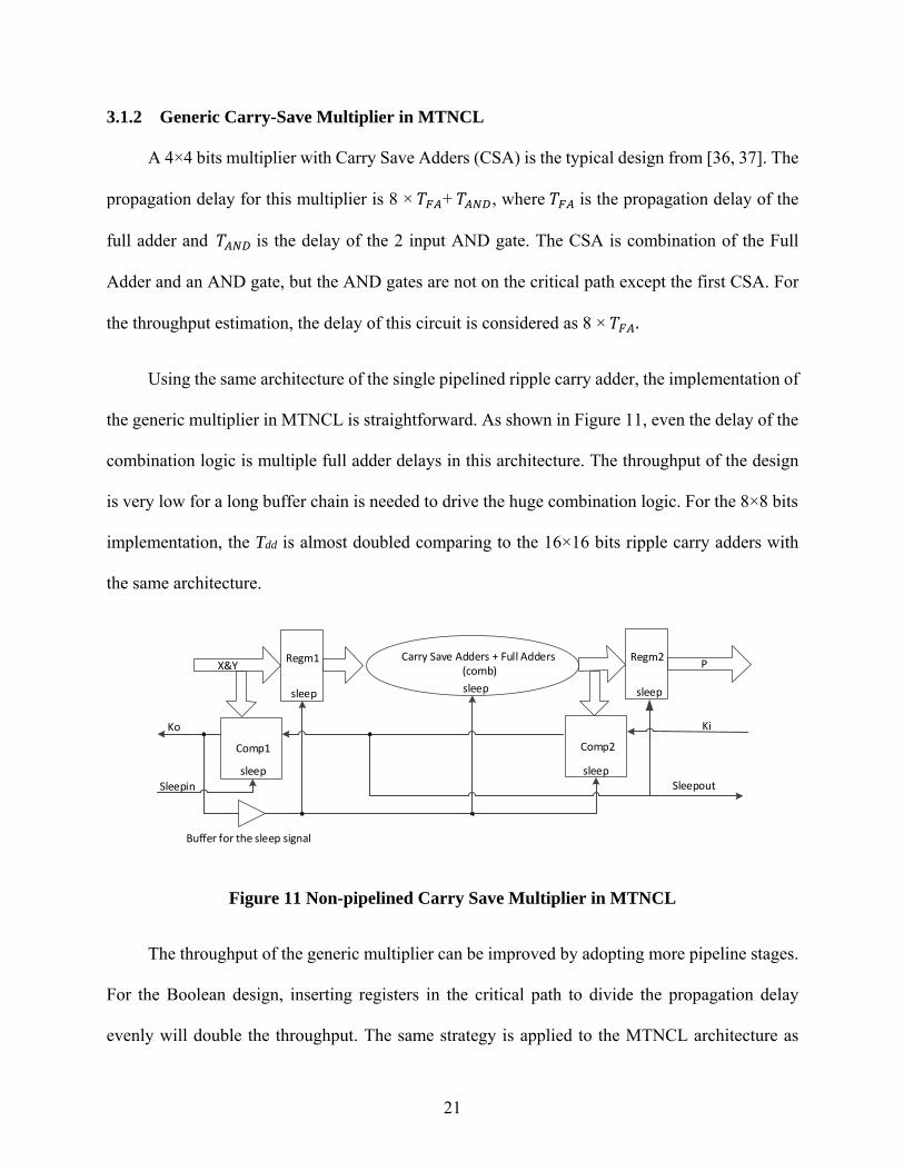
3.1.2 Generic Carry-Save Multiplier in MTNCL
A 4×4 bits multiplier with Carry Save Adders (CSA) is the typical design from [36, 37]. The
propagation delay for this multiplier is 8 × + , where is the propagation delay of the
full adder and is the delay of the 2 input AND gate. The CSA is combination of the Full
Adder and an AND gate, but the AND gates are not on the critical path except the first CSA. For
the throughput estimation, the delay of this circuit is considered as 8 × .
Using the same architecture of the single pipelined ripple carry adder, the implementation of
the generic multiplier in MTNCL is straightforward. As shown in Figure 11, even the delay of the
combination logic is multiple full adder delays in this architecture. The throughput of the design
is very low for a long buffer chain is needed to drive the huge combination logic. For the 8×8 bits
implementation, the Tdd is almost doubled comparing to the 16×16 bits ripple carry adders with
the same architecture.
sleep
Comp1
sleep
Regm1
sleep
Comp2
sleep
Regm2
sleep
Ko
Sleepin Sleepout
Ki
PX&Y
Buffer for the sleep signal
Carry Save Adders + Full Adders (comb)
Figure 11 Non-pipelined Carry Save Multiplier in MTNCL
The throughput of the generic multiplier can be improved by adopting more pipeline stages.
For the Boolean design, inserting registers in the critical path to divide the propagation delay
evenly will double the throughput. The same strategy is applied to the MTNCL architecture as
22
shown in Figure 12. From equation (3), the Tdd of the MTNCL pipeline is not only determined by
the delay of the combination logic. For the two pipeline stages in Figure 12, _ ,
_ and are the same. But the combination logic in stage 1 is much larger than
the combination logic in stage 2. After buffering the sleep signal, _ will be larger than
_ . Since the circuit throughput is constrained by the maximum Tdd in the pipeline stages;
the throughput of the two pipelined architecture will be deteriorated as the number of input bits
scale up. However, when the number of input bits is fixed as 8, the combination logic in the two
pipeline stages can be driven by the same buffer. With the balanced Tdd in the two pipeline stages,
the throughput is improved by partitioning the combination logic.
sleep
Comp1
sleep
Regm1
sleep
Comp
sleep
Regm
sleep
Ko
Sleepin
Carry Save Adders(comb1)
sleep
Comp2
sleep
Regm2
sleep
Sleepout
Ki
Full Adders(comb2) PX&Y
Pipeline stage 1 Pipeline stage 2
Figure 12 Pipelined Carry Save Multiplier in MTNCL
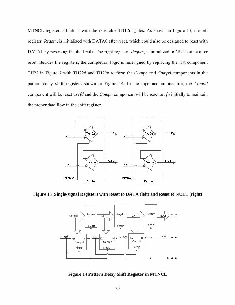
3.1.3 Delay Units in MTNCL
The Delay Units in the synchronous circuit are shift registers, which are a serial of D Flip-
Flops with previous output connected to the next input. When the clock rises, the data will go
through the data path. However, the asynchronous pipeline is incapable of building the shift
register as in the synchronous one. The initial states for the registers are logic 0 with reset and
logic 1 with set in the synchronous circuit, while the registers in MTNCL all go to NULL and Ko
goes to rfd after reset. To maintain the DATA/NULL pattern in the delay chain, a new type of
23
MTNCL register is built in with the resettable TH12m gates. As shown in Figure 13, the left
register, Regdm, is initialized with DATA0 after reset, which could also be designed to reset with
DATA1 by reversing the dual rails. The right register, Regnm, is initialized to NULL state after
reset. Besides the registers, the completion logic is redesigned by replacing the last component
TH22 in Figure 7 with TH22d and TH22n to form the Compn and Compd components in the
pattern delay shift registers shown in Figure 14. In the pipelined architecture, the Compd
component will be reset to rfd and the Compn component will be reset to rfn initially to maintain
the proper data flow in the shift register.
Figure 13 Single-signal Registers with Reset to DATA (left) and Reset to NULL (right)
CompdKo Ki
sleep
Regnm
sleep
CompnKo Ki
sleep
Regdm
sleep
rfd
CompdKo Ki
sleep
Regnm
sleep
NULL DATA
rfn rfd rfn
Figure 14 Pattern Delay Shift Register in MTNCL
24
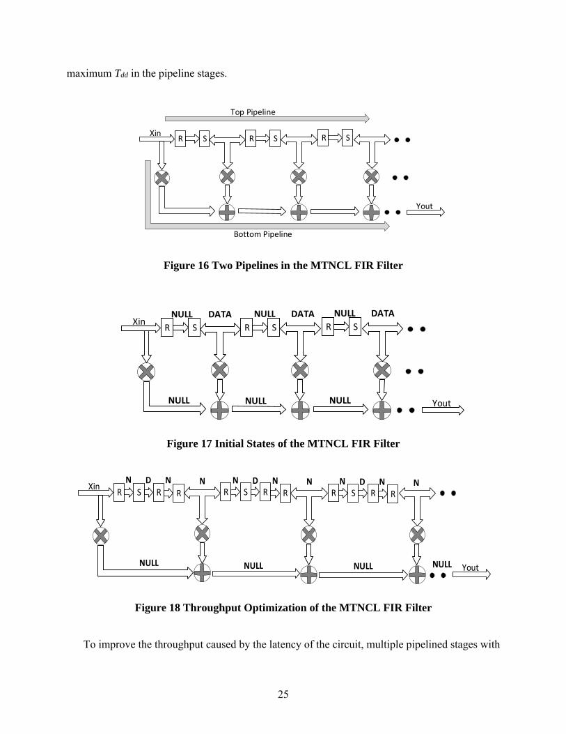
3.1.4 FIR Circuit Design and Throughput Optimization
The individual components, including the shifter register, the adders and the multipliers,
compose a tap-generic FIR filter with fixed 8-bit input. The structure is shown in Figure 15. There
are two pipeline stages in this architecture as marked in Figure 16, the bottom one convolutes the
input data and the top one shifts the input data. This circuit works and produces correct result. But
the throughput is not optimized.
Z‐1 Z‐1 Z‐1 Z‐1Xin
Yout
Figure 15 Architecture of the FIR Filter
For the two pipelines architecture, after reset, the data path in the bottom one are all in ‘NULL’
cycle. While the data path in the top pipeline is reset to ‘DATA’ and ‘NULL’ patterns for it was
designed as the pattern delay shift register. The bottom pipeline is considered as ‘empty’ and the
top pipeline as already ‘full’ after reset. The DATA can propagate through an ‘empty’ pipeline but
need to extrude a DATA to enter a ‘full’ pipeline, as shown in Figure 17. When the first external
data comes into the pipelines, it propagates through the bottom pipeline but blocks at the first
register in the top pipeline. After propagation delay of the bottom pipeline, which is the latency in
a pipeline circuit, the top pipeline can move forward and those two pipelines will be able to take
in next data. So the throughput of this architecture is the reciprocal of the latency, rather than the
25
maximum Tdd in the pipeline stages.
Xin
Yout
R S R S R S
Top Pipeline
Bottom Pipeline
Figure 16 Two Pipelines in the MTNCL FIR Filter
Xin
Yout
R S R S R SNULL DATA NULL DATA NULL DATA
NULL NULL NULL
Figure 17 Initial States of the MTNCL FIR Filter
Xin
YoutNULL NULL NULL NULL
R S R R R S R R R S R R
N D N N N D N N N D N N
Figure 18 Throughput Optimization of the MTNCL FIR Filter
To improve the throughput caused by the latency of the circuit, multiple pipelined stages with
26
NULL cycle initialization are implemented in the top pipeline, as shown in Figure 18. After reset,
the top pipeline has the same number of ‘NULL’ cycles as the bottom one, then the DATA in the
top pipeline can move forward after internal data comes in.
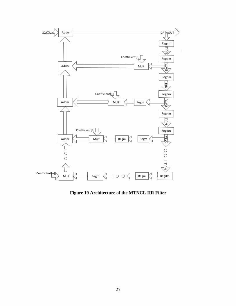
3.2 Design of the Infinite Impulse Response (IIR) Filter
Different with the feeding forward structure in the FIR filter, the IIR filter has a recursive
structure. The feedback from the output is used in the next convolution stage, which may lead to
unstable output. The recursive part of the IIR filter is implemented in the MTNCL circuit. To
prevent the output going to infinite, the digitals in the data flow are encoded in a fixed point number
with fractional bits, which is called Q format in the arithmetic requiring constant resolution. In
the IIR circuit, the input and output bits are all constrained to 16. The data format is Q1.15 with a
range of [-1, 1) with a resolution of2 .
The IIR architecture also requires multipliers, adders and the delay chain. Since the data format
in IIR circuit is signed, the generic multiplier and adder used in the FIR circuit are changed to
adopt the signed value operation. The multiplier is changed to Baugh-Wooley architecture [38]
with the 2 pipeline stages. An overflow detection bit is added to the generic adder to indicate when
there is an overflow in the addition. The delay chain is kept exactly the same as the FIR design for
throughput optimization. Since the data width is 16 bits in the IIR, the maximum delay in the
circuit is the 2-stage multiplier. The architecture of the IIR filter is shown in Figure 19.
27
DATAIN Adder
Coefficient[0]
Mult
Mult
Regm
Regm RegmMult
Adder
Adder
Adder
Coefficient[1]
Coefficient[3]
DATAOUT
Regm RegmMultCoefficient[n]
Figure 19 Architecture of the MTNCL IIR Filter
28
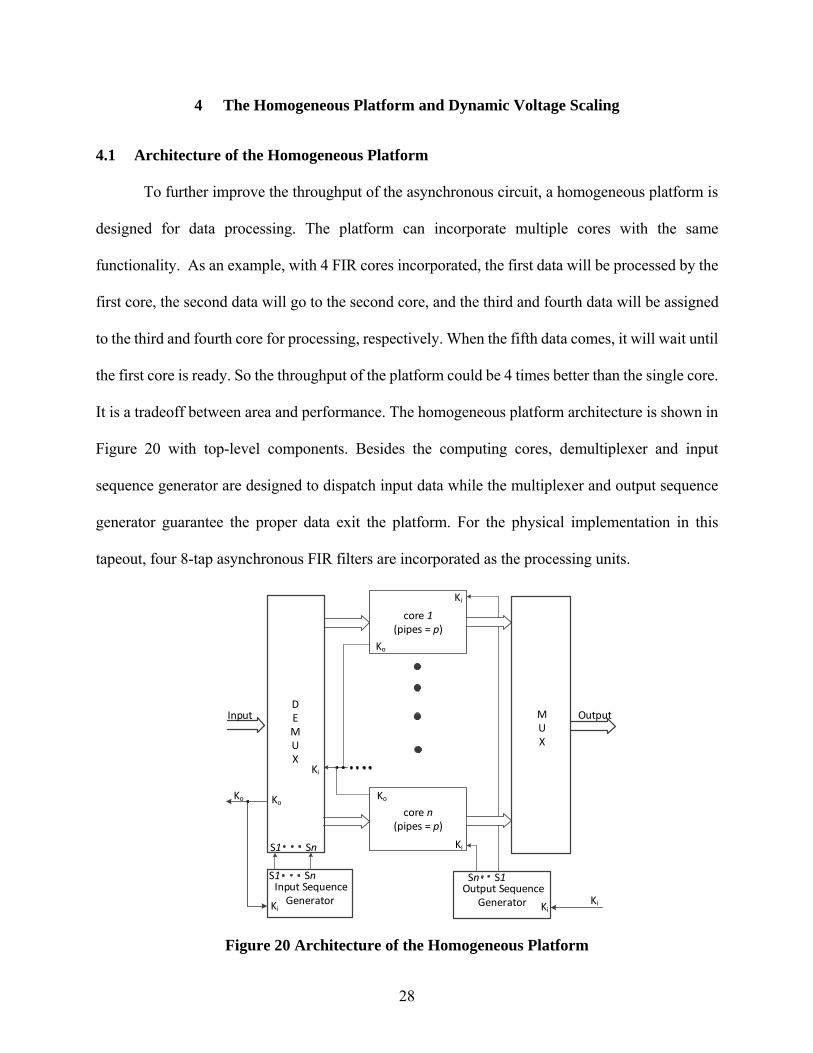
4 The Homogeneous Platform and Dynamic Voltage Scaling
4.1 Architecture of the Homogeneous Platform
To further improve the throughput of the asynchronous circuit, a homogeneous platform is
designed for data processing. The platform can incorporate multiple cores with the same
functionality. As an example, with 4 FIR cores incorporated, the first data will be processed by the
first core, the second data will go to the second core, and the third and fourth data will be assigned
to the third and fourth core for processing, respectively. When the fifth data comes, it will wait until
the first core is ready. So the throughput of the platform could be 4 times better than the single core.
It is a tradeoff between area and performance. The homogeneous platform architecture is shown in
Figure 20 with top-level components. Besides the computing cores, demultiplexer and input
sequence generator are designed to dispatch input data while the multiplexer and output sequence
generator guarantee the proper data exit the platform. For the physical implementation in this
tapeout, four 8-tap asynchronous FIR filters are incorporated as the processing units.
core 1(pipes = p)
Ko
DEMUX
core n(pipes = p)
Ko
MUX
Ki
Input Output
Ki
Ki
Input Sequence Generator
S1 Sn
S1 Sn
Ko
Output Sequence Generator
Sn S1
Ko
Ki KiKi
Figure 20 Architecture of the Homogeneous Platform
29
Ko
Input
DEMUX MUX
Input Sequence Generator
Output Sequence Generator Ki
I
Ko
C
D
S1 S2
S1 S2 S1S2
Ko
Ko
Ki
Ki
Ki
C
D
Z Output
KiS3 S4
S3 S4
A
B
A
B
S3S4
Ki
Voltage Control Unit
Cores’ VDD
Ko Ki
Core1(Pipes = p)
Ko Ki
Core2(Pipes = p)
Ko Ki
Core3(Pipes = p)
Ko Ki
Core4(Pipes = p)
Ko Ki
VDD
VDD
VDD
VDD
Input
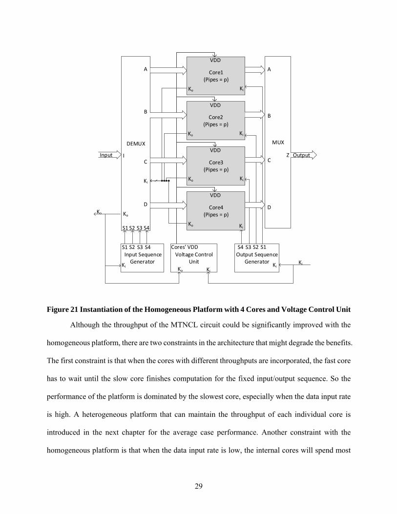
Figure 21 Instantiation of the Homogeneous Platform with 4 Cores and Voltage Control Unit
Although the throughput of the MTNCL circuit could be significantly improved with the
homogeneous platform, there are two constraints in the architecture that might degrade the benefits.
The first constraint is that when the cores with different throughputs are incorporated, the fast core
has to wait until the slow core finishes computation for the fixed input/output sequence. So the
performance of the platform is dominated by the slowest core, especially when the data input rate
is high. A heterogeneous platform that can maintain the throughput of each individual core is
introduced in the next chapter for the average case performance. Another constraint with the
homogeneous platform is that when the data input rate is low, the internal cores will spend most
30
of the time in idle state waiting for the data coming in. In that case the energy efficiency of the
platform could be worse than a single core because of the high leakage from the area overhead. In
this chapter, a Dynamic Voltage Scaling (DVS) method is applied to the asynchronous
homogeneous platform for energy efficiency.
4.2 DVS for the Homogeneous Platform
The self-timed circuit can tolerate a large supply voltage range because the delay caused
by voltage drop will not affect its functionality. The minimum supply voltage to the MTNCL
circuit is the Voltage that can sustain the properly operation of the transistors. Dynamic voltage
scaling has great potential to improve the energy efficiency of the multi-core asynchronous
platform when the data input rate is low. The architecture for the homogenous platform with DVS
controller is shown in Figure 21. In this architecture, the platform is divided into two voltage
domains. The demultiplexer, the multiplexer and input/output sequence generators are working
with maximum voltage supply; so the input data can be dispatched to the internal cores at the
maximum speed. Another domain is the supply voltage to the internal cores, which can be adjusted
dynamically according to the data input rate. When the data input rate is high, the cores work at
the maximum voltage supply for best performance. On the other hand, the supply voltage drops
and the speed of the core is traded off for energy efficiency.
The Voltage Control Unit (VCU) as shown in Figure 22 is the component that implements
dynamic voltage scaling on the platform. The basic function of the VCU is detecting the input data
rate variation and quantizing the variation into reference in a range of minimize and maximum
supply voltage. The latency of the MTNCL pipeline is used to design detection circuit. With
various scenarios of input data variation, the prediction circuit is designed to make the VCU
31
efficient in more complex situation. And the reference voltage is used by a 2-stage current sensor
based voltage regulator for supply voltage adjustment.
Pipeline Fullness Detector
Ki Counter
Ko Counter
Subtrac-ter
Fullness Predictor
Vref Generator
Voltage Regulator
Cores’VDD
Ko
Ki
Voltage Control Unit
Figure 22 Internal Structure of the Voltage Control Unit
4.2.1 Latency of the MTNCL Pipeline
The latency in a pipelined circuit is the delay between the first input data and the first output
data. Inside the voltage controller, the latency of the MTNCL pipeline serves as a timing period to
quantize the input data rate. In a Boolean pipelined architecture, the latency of the circuit depends
on the clock period and number of pipeline stage. And the clock period is dominated by the set up
and hold times of the register, the maximum combination delay between the pipeline stages and
the clock skew. So the Boolean circuit usually has the worst case performance in terms of latency.
The latency in the Boolean pipeline cannot be used to for data input quantization because they are
both related to clock frequency. However, the MTNCL circuit has the average case performance
feature. As each DATA cycle will propagate through the register, the combination block and the
completion detection block in the initialized NULL stages. So the latency of the MTNCL pipeline
is the propagation delay from the input port to the output port, which is independent of the input
data rate.
32
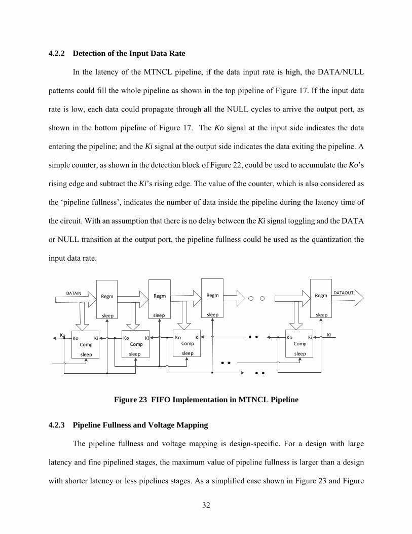
4.2.2 Detection of the Input Data Rate
In the latency of the MTNCL pipeline, if the data input rate is high, the DATA/NULL
patterns could fill the whole pipeline as shown in the top pipeline of Figure 17. If the input data
rate is low, each data could propagate through all the NULL cycles to arrive the output port, as
shown in the bottom pipeline of Figure 17. The Ko signal at the input side indicates the data
entering the pipeline; and the Ki signal at the output side indicates the data exiting the pipeline. A
simple counter, as shown in the detection block of Figure 22, could be used to accumulate the Ko’s
rising edge and subtract the Ki’s rising edge. The value of the counter, which is also considered as
the ‘pipeline fullness’, indicates the number of data inside the pipeline during the latency time of
the circuit. With an assumption that there is no delay between the Ki signal toggling and the DATA
or NULL transition at the output port, the pipeline fullness could be used as the quantization the
input data rate.
CompKo Ki
sleep
Regm
sleep
CompKo Ki
sleep
Regm
sleep
CompKo Ki
sleep
Regm
sleep
Ko
CompKo Ki
sleep
Regm
sleep
Ki
DATAIN DATAOUT
Figure 23 FIFO Implementation in MTNCL Pipeline
4.2.3 Pipeline Fullness and Voltage Mapping
The pipeline fullness and voltage mapping is design-specific. For a design with large
latency and fine pipelined stages, the maximum value of pipeline fullness is larger than a design
with shorter latency or less pipelines stages. As a simplified case shown in Figure 23 and Figure
33
24 (a), in a FIFO buffer without any combination logic between the registers, the maximum
fullness value is evaluated by equation (1).
_
(1)
and are the propagation delay of the register and completion detection block in the
MTNCL pipeline.
If combination logic is put at the first pipeline stage of the MTNCL circuit as shown in
Figure 24 (b), the maximum fullness value will be significantly reduced because the delay of the
combination block will be applied to each the DATA/NULL cycle in the latency time. The
equation (1) used for maximum fullness detection will be changed to equation (2).
_
(2)
The third structure is putting the FIFO buffer before the pipeline stages with combination
logic, as shown in Figure 24 (c). In that case, the latency can be divided into two parts, the latency
of the FIFO and the latency of the logic. The maximum fullness value can be evaluated by equation
(3).
_ _
_
(3)
Equation (3) shows that in a pipelined circuit that with combination logic, the maximum
fullness detected by counting the handshaking signals can be increased by buffering the input data.
Since the pipeline fullness is used for dynamic voltage scaling, increasing the maximum detectable
fullness value can improve the resolution of voltage control.
34
R R R R R R
(a) Pipeline without Combination Logic
R C R R R R R R R
(b) Combination Logic at the Head of the Pipeline
R R C R R RR R R
(c) Combination Logic in the Middle of the Pipeline
Figure 24 Latency Estimation of Three Different MTNCL Pipelines
4.2.4 Pipeline Fullness Observation
The test vehicle for the homogenous platform is instantiated with 4 FIR cores; each with 8
taps as the computing units in the platform. As discussed in the previous section, buffers with 4
pipeline stages are inserted into the platform to improve the voltage scaling resolution. The fullness
of the platform is observed with the core’s VDD fixed to various voltage supplies and maximum
workload. When the supply voltage is high, the processing core works fast and pipeline fullness
stays low. With maximum workload for the observation, the pipeline accumulates maximum
number of data at the minimum operating voltage. Table 3 shows the pipeline fullness variation
with the supply voltage in an adjustable range. A linear characteristic is used to construct a voltage
35
divider network, with maximum fullness in the platform pipeline converted to 1.2 V and minimum
fullness mapping to 0.6 V.
Table 3 Pipeline Fullness Observation
Core’s VDD 0.6V 0.7V 0.8V 0.9V 1.0V 1.1V 1.2V
Fullness 12 10 9 8 7 6 5
4.2.5 Workload Prediction Circuit
The prediction algorithm is used to make more effectively control of the dynamic voltage
scaling across various input scenarios. As a counter is designed to accumulate the Ko’s rising edge
and subtract the Ki’s rising edge, the value of which indicates the number of DATA inside the
pipeline during the latency time. As the decision-making unit for generating the voltage control
signals, the pipeline fullness detection circuit is the key component in DVS for real-time energy
optimization. Comparing the detected fullness with the pre-configured value, the control algorithm
could simply raise or lower down the voltage. Due to the delay insensitivity of MTNCL, the
platform is able to tolerate the delay overhead caused by adjusting VDD, without losing data or
malfunctioning. However, for certain applications where input data bursts are common, the
throughput adjusting may lag behind the input variations and degrade the overall performance.
Even though a long data buffer could be applied to register all input data, the overhead will be
worse in terms of energy consumption. Therefore, a workload predictor is developed to enhance
the DVS control mechanism.
As an example in the homogenous platform implemented with four FIR coes, the pipeline
fullness detector has a 4-bit binary output, with an entire state space comprising 16-fold history.
36
However, implementing 16 states in hardware will cause high overhead. As the pipeline fullness
in the platform is always continuously changing with the handshaking signals, the simplified
algorithm could be predicting the acceleration of the pipeline fullness, as well as tracing the
previous history.
In the prediction circuit, the output of pipeline fullness detector, Q, is latched by the
external input signal sleepin. The fullness acceleration is reduced to 3 states, which are Riseup,
DonotChange, and Lowdown, in one-hot encoding. The acceleration state is predicted in a finite
state machine (FSM) and applies to the registered Q for generating the predicted fullness, PreQ.
In the following DATA cycle, PreQ will be evaluated to produce a miss or hit signal, depending
on weather PreQ and Q is equal or not. The miss or hit signal will update the FSM and predict the
subsequent fullness acceleration.
SR[10] WR[10] DC[00] SL[01]WL[01]
hit
hit
hit
hit
hitmissmiss
[01]miss
[10]miss
Figure 25 State Machine for Work Load Prediction. SR and SL states are for Riseup[10] prediction; WR and WL states are for Lowdown[01]; DC state produces DonotChange[00] prediction. The hit signal means the current state has made a right prediction of fullness acceleration. The miss signal for WR, DC and WL states is combined with flag of real production, e.g., [01]miss indicates the predictor was off target with the actual acceleration, which is Lowdown[01].
The state switch mechanism imitates the 2-way branch predictor [39] utilized to improve
the flow in the instruction pipeline. Five states, SR (strongly rise-up), WR (weakly rise-up), SL
37
(strongly low-down), WL (weakly low-down) and DC (don’t care) are encoded in the FSM. In the
states of SR [strongly Riseup] and WR [weakly Riseup], the prediction result of q' is Riseup. In the
states of SL [strongly Lowdown] and WL [weakly Lowdown], the prediction result of q' is
Lowdown. In the state of DC, the prediction result of q' is DonotChange. The transition of the
states is based on the prediction result is ‘miss’ or ‘hit’. Between WR, DC and WL, the states
transition also depends on the value of q besides ‘miss’ and ‘hit’, while in other states, previous
acceleration is employed besides this signal, as illustrated in Figure 25.
4.2.6 Voltage Regulator
The parallel cores of the platform are driven by a VDD supplied from the voltage regulator.
It dynamically adjusts the output voltage according to the reference value from the Vref generator.
As shown in Figure 26, the voltage regulator has a simple circuit structure to achieve fast output
voltage scaling speed for real-time adaptability. Transistors P2, P3, P4, N1 and N2 form an
operational amplifier. Combined with the pass device formed by P5 and R2, the negative feedback
loop keeps the output Vout following Vref’s adjustment with a large drive capability. P1 and P2 form
a current mirror to provide the operation current for the operational amplifier. N3 works as a bypass
capacitor to improve the stability of the negative loop. The supply voltage for the regulator is fixed
to 1.5 V for a maximum output of 1.2 V.
38
Vref VoutR1
R2
N3N2N1
P4P3
P2P1 P5
Vdd
GND
Figure 26 Circuit of the Voltage Regulator
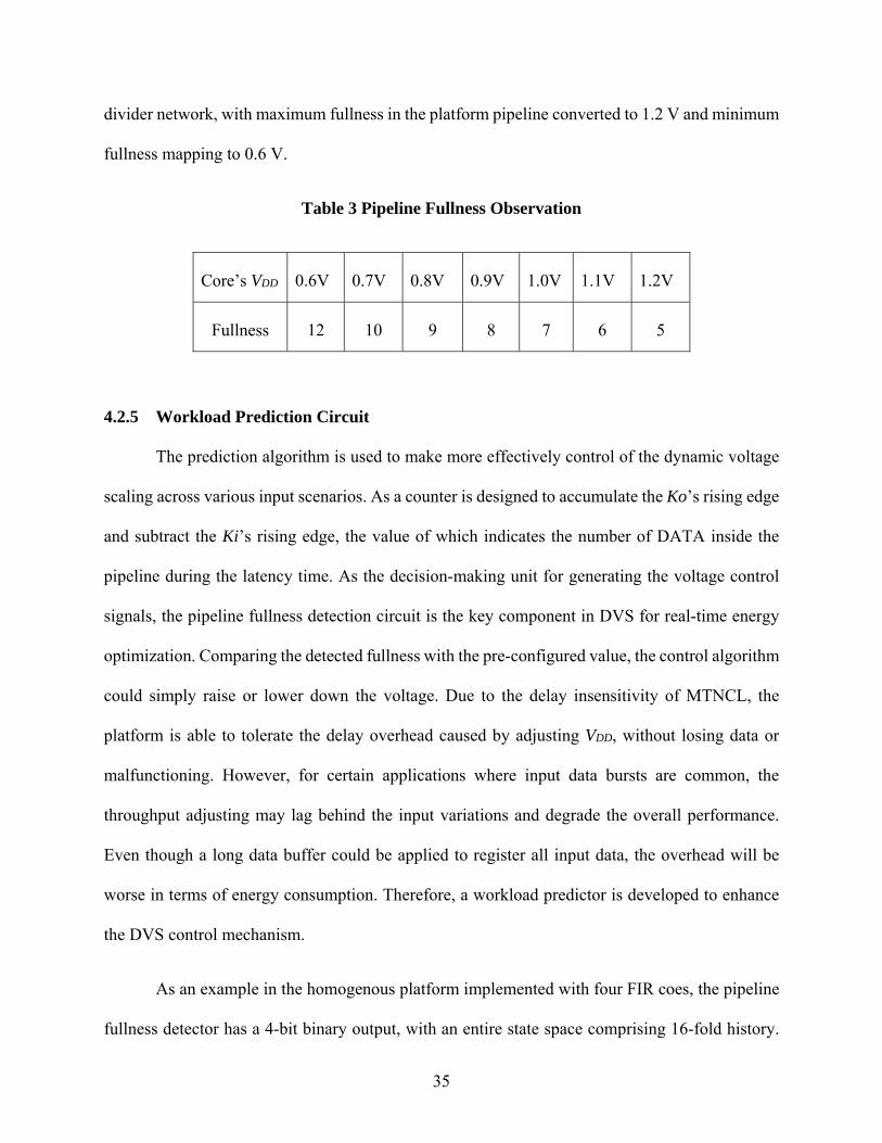
4.3 Homogeneous Platform for Synchronous Circuit
To evaluate the efficiency of the DVS mechanism of the homogeneous platform, a
synchronous counterpart is designed with the same functionality. As shown in Figure 27, the
synchronous platform is built with de-multiplexer, multiplexer, internal cores and a clock divider.
The supply voltage to the cores is adjustable; and a voltage control unit is implemented for dynamic
voltage scaling. Different from the asynchronous platform, where the pipeline structure can be
viewed as an FIFO for data input rate evaluation, all the internal status of the synchronous platform
change with the global clock. The variation of the input data rate cannot be reflected by the
synchronous pipeline. An external asynchronous FIFO is used to detect the variation of the input
data rate variation, with a depth of 16 to match the pipeline status of the asynchronous platform.
The ‘status’ output of the FIFO indicates the number of data possessed. The DVS component could
be a similar design as the asynchronous one, predicting the input data rate by the variation of the
FIFO status. For the DVS control, the supply voltage of the computing cores could be adjusted
39
dynamically and the voltage for the other components, including the MUX, DEMUX, the clock
divider, the asynchronous FIFO and the DVS components, is fixed to the maximum supply.
clk
DEMUX
Core3
Core 4
MUX
ClockDivider
I C
D
C
D
Z Output
Core1
Core2
A
B
A
B
clk
Voltage Control Unit
Cores’ VDD
clk
clk
clk clk
Asynchronous FIFO
Input
status
Clock
Wr_clk Rd_clk
empty
Full
Figure 27 Synchronous Count Part of the Homogeneous Platform
2‐bit Counter
4‐input MUX
S0 S1
4‐input MUX
S0 S1
4‐input MUX
S0 S1
Core0_D0
Core1_D0
Core2_D0
Core3_D0
Core0_D1
Core1_D1
Core2_D1
Core3_D1
Core0_D22
Core1_D22
Core2_D22
Core3_D22
Dataout0 Dataout1 Dataout22
Clock
Figure 28 Demultiplexer in the Synchronous Homogeneous Platform
40
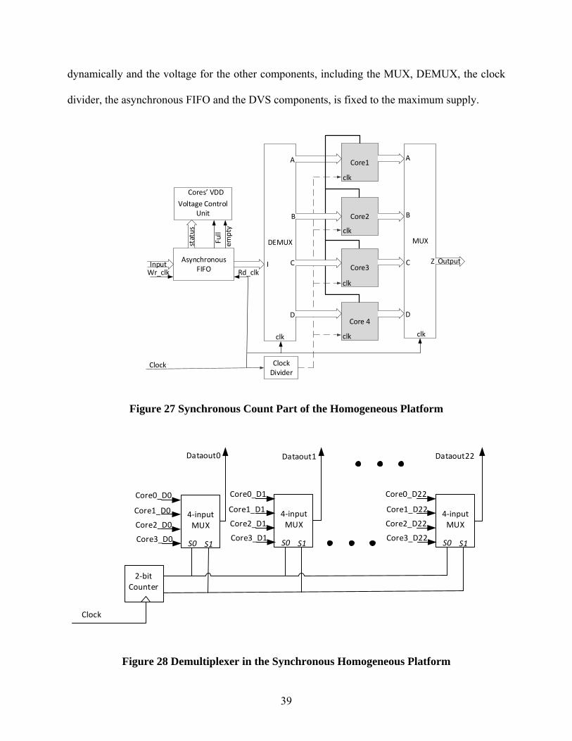
In the diagram with 4 computing cores, the de-multiplexer is built with a 2-bit counter, a
2-4 decoder and registers, as shown in Figure 28. The input data can be dispatched to the internal
cores sequentially following the input clock. The multiplexer is built with a 2-bit counter and 4-
input multiplexers, as shown in Figure 29. The outputs of the cores are merged into the output of
the platform following the input clock. Inside the platform, the computing cores can operate at the
speed of one-quarter of the clock frequency, while the output of the platform is synchronized with
the clock.
AND
2‐bit Counter
2 to 4 Decoder
AND
AND
AND
DFFs
DFFs
DFFs
DFFs
DATAIN
clk
Figure 29 Multiplexer in the Synchronous Homogeneous Platform
For the dynamic voltage scaling, the asynchronous platform with micro-pipeline can be
viewed as an FIFO with internal logic. The platform itself can detect the input data rate variation.
In the synchronous platform, all the internal status changes with the external clock, which cannot
reflect the variation of the input data. An asynchronous FIFO is used to buffer the input data and
detect the variation of the input data rate, with a depth of 16 to match the pipeline status of the
asynchronous platform. The ‘status’ output of the FIFO indicates the number of data possessed.
The DVS component could be a similar design as the asynchronous one, predicting the input data
41
rate by the variation of the FIFO status. For the DVS control, the supply voltage of the computing
cores could be adjusted dynamically and the voltage for the other components, including the MUX,
DEMUX, the clock divider, the asynchronous FIFO and the DVS components, is fixed to the
maximum supply.
WriteAddress
ReadAddress
FIFO Memory
DATAIN DATAIN DATAOUT
FIFO WptrGeneration
waddr
wptr
Synchronizer
Synchronizer
FIFO RptrGeneration
raddr
rptr
Status
S_wptrS_rptr
wfull rempty
wclken
rstrst
Wr_clk
reset
Rd_clk
emptyFull
Figure 30 Architecture of the FIFO in the Synchronous Homogeneous Platform
The diagram of the asynchronous FIFO is shown in Figure 30. Four components, the FIFO
memory, the read/write pointer generator, and the synchronizer, are inside the FIFO. The FIFO
memory is a dual port RAM, with a depth of 16 and input/output of 8 bits. The write operation to
the memory is controlled by the write clock (Wr_clk) and the write enable (wclken) signal. The
read operation of the memory depends on the changes of the read address. The control components
for the memory are the read and writer pointer generators. The read/write pointer generator
increments the pointer value in gray code following the read/write clock. The pointer values are
converted to binary as the address for the FIFO memory. To detect if the memory is full or empty,
42
the read/write pointer needs to be synchronized to the write/read domain through the write/read
clock. After the synchronization, the read pointer and writer pointer are compared in gray code to
decide if the read pointer is catching up the writer pointer, which is an empty signal, or the write
point is catching up the read pointer, which is a full signal.
43
5 The Heterogeneous Platform and Scalability
5.1 Heterogeneous Platform Design Overview
As presented the Chapter 4, the platform architecture has a tradeoff between area and
performance. The homogeneous platform with DVS addresses the issue that when the data input
rate is low, the energy and performance are balanced by dynamically adjusting the supply voltage
to the processors. However, when the data input rate is high and cores with different capabilities
are incorporated, the performance of the platform will be degraded by the slowest core such that
all faster cores need to wait for the slowest core to finish before requesting the next batch of data,
which is similar to an unbalanced pipeline. In this chapter, a heterogeneous platform architecture
is designed to improve the performance under such conditions.
When the input and output data sequences are fixed as in the homogeneous architecture,
the platform will have the worst-case performance when the cores with different throughput are
incorporated. To avoid that scenario, the platform needs to be able to dispatch data to a core as
soon as it requests for data. However, there could be collisions if more than one autonomous
operating core is requesting for data within a short period of time. To prevent collision, an
arbitration mechanism is necessary to grant mutually exclusive access to the common data bus of
the platform. The worst case of the system throughput could be avoided by assigning the highest
priority to the slowest core in the platform when collision happens.
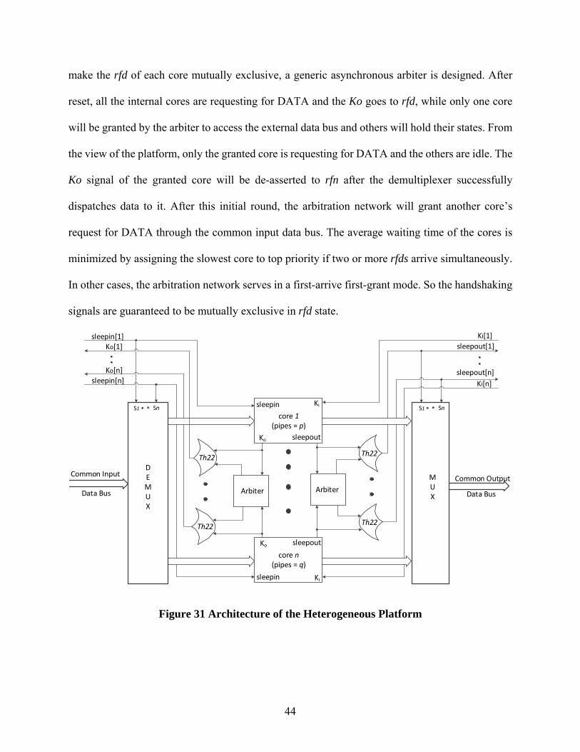
5.2 Architecture of Heterogeneous Platform
A generic heterogeneous platform incorporating n cores is designed as shown in Figure 31.
The handshaking signals of each core are reserved and separated from the common data bus. To
44
make the rfd of each core mutually exclusive, a generic asynchronous arbiter is designed. After
reset, all the internal cores are requesting for DATA and the Ko goes to rfd, while only one core
will be granted by the arbiter to access the external data bus and others will hold their states. From
the view of the platform, only the granted core is requesting for DATA and the others are idle. The
Ko signal of the granted core will be de-asserted to rfn after the demultiplexer successfully
dispatches data to it. After this initial round, the arbitration network will grant another core’s
request for DATA through the common input data bus. The average waiting time of the cores is
minimized by assigning the slowest core to top priority if two or more rfds arrive simultaneously.
In other cases, the arbitration network serves in a first-arrive first-grant mode. So the handshaking
signals are guaranteed to be mutually exclusive in rfd state.
core 1(pipes = p)
Ko
DEMUX
Arbiter
core n(pipes = q)
Ko sleepout
sleepout
Arbiter
MUX
sleepin
sleepin Ki
Common Input
Data Bus
Common Output
Ki
Ki[1]
sleepout[1]
Ki[n]
sleepout[n]
sleepin[1]Ko[1]
sleepin[n]
Ko[n]
Th22
Th22
Th22
Th22
Data Bus
S1 Sn S1 Sn
Figure 31 Architecture of the Heterogeneous Platform
45
5.3 Multiplexer and Demultiplexer Design with NULL Cycle Reduction
NULL Cycle Reduction (NCR) [40] is used to increase the throughput of NCL systems by
reducing the NULL cycle on the I/O port in the multi-core architectures. In the heterogeneous
platform, the external ports for all the handshaking signals of the internal cores facilitate the
implementation of the NCR technique in the demultiplexer and multiplexer.
DEMUX_datain
core[0]_sleepin
bufm
bufm
bufm
core[1]_sleepin
core[n]_sleepin
core 0datain
core 1datain
core ndatain
Figure 32 Demultiplexer in the Heterogeneous Platform
The demultiplexer partitions the common input data bus to n output data paths connecting
to the internal cores. The data dispatching operation is controlled by the exclusive sleepin signals.
Figure 32 shows the structure design of the demultiplexer. The bufm is a basic MTNCL buffer.
When the sleep signal is active, the output is forced to be ‘0’; otherwise it follows its input. By
inserting the bufm gate into all the rails of the input data path, the demultiplexer outputs a NULL
wave after reset, when all the sleepin signals are active. In the heterogeneous platform, the rfd
states of the cores are mutually exclusive, which means no more than one sleepin signals can be
deactivated per arbitration; so only the rfd granted core’s datapath will connect to the common
46
input data bus during the DATA wave. The demultiplexer will automatically generate a NULL
wave onto the datapath of the asynchronous core if its rfd is not granted. This simplifies the
common input data bus interface, for it does not need to incorporate a NULL spacer when
switching among different input data.
dataout.rail1
bufm
bufm
Core[0].rail0
Core[0].rail1
Core[0]_sleepout
bufm
bufm
Core[1].rail0
Core[1].rail1
Core[1]_sleepout
bufm
bufm
Core[n].rail0
Core[n].rail1
Core[n]_sleepout
ORtree
ORtree
Th22
Th22dataout.rail0
Figure 33 NCR Multiplexer in the Heterogeneous Platform
The multiplexer is designed in a similar fashion. It multiplexes all the outputs of the internal
cores onto one single output data bus for the platform. Again, MTNCL buffer gates – this time
with exclusive sleepout signals per core – are employed on all the rails of the core’s output
datapaths to ensure only one core produces DATA states. To eliminate the NULL spacer on the
common output bus, the DATA state of the core with output data bus access is held by the OR tree
47
and the C-element gate (TH22) until the next core’s data output request is granted. Figure 33 shows
the structure of the NCR multiplexer with one bit output form multiple cores. The output from the
multiplexer switches between the DATA states of the internal cores following a pattern similar to
that of the common input data bus. The output order may be different with the input order. This
configuration produces a scalable heterogeneous platform.
5.4 Asynchronous Arbiter Design
The handshaking components require that the communication along several input channels
is mutually exclusive. The basic circuit needed to deal with such situations is a mutual exclusion
element (MUTEX) [41], shown in Figure 34. The circuit contains a latch with NAND gates and a
metastable filter. The input signals R1 and R2 are two requests that originate from two independent
sources, and the task of the MUTEX is to pass these inputs to the corresponding outputs G1 and
G2 in such a way that at most one output is active at any given time. If only one input request
arrives, the operation is trivial. If one input request arrives well before the other, the latter request
is blocked until the first request is de-asserted. When both inputs are asserted at the same time, the
MUTEX is required to make an arbitrary decision, and this is where metastability enters the
picture.
GND
Latch Filter
R1
R2
G1
G2
Figure 34 Mutual Exclusion Element (MUTEX) in Transistor-Level Implementation
48
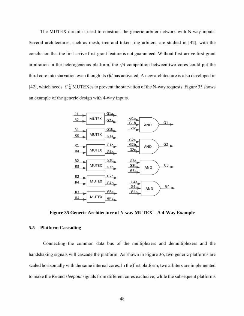
The MUTEX circuit is used to construct the generic arbiter network with N-way inputs.
Several architectures, such as mesh, tree and token ring arbiters, are studied in [42], with the
conclusion that the first-arrive first-grant feature is not guaranteed. Without first-arrive first-grant
arbitration in the heterogeneous platform, the rfd competition between two cores could put the
third core into starvation even though its rfd has activated. A new architecture is also developed in
[42], which needs MUTEXes to prevent the starvation of the N-way requests. Figure 35 shows
an example of the generic design with 4-way inputs.
MUTEXR1
R2
G1a
G2a
MUTEXR1
R3
G1b
G3a
MUTEXR1
R4
G1c
G4a
MUTEXR2
R3
G2b
G3b
MUTEXR2
R4
G2c
G4b
MUTEXR3
R4
G3c
G4c
G1aG1b
G1c
G1AND
G2AND
G3aG3b
G3c
G3AND
G4aG4b
G4c
G4AND
G2aG2b
G2c
Figure 35 Generic Architecture of N-way MUTEX – A 4-Way Example
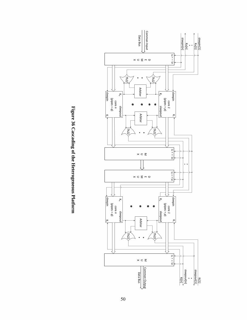
5.5 Platform Cascading
Connecting the common data bus of the multiplexers and demultiplexers and the
handshaking signals will cascade the platform. As shown in Figure 36, two generic platforms are
scaled horizontally with the same internal cores. In the first platform, two arbiters are implemented
to make the Ko and sleepout signals from different cores exclusive; while the subsequent platforms
49
just need one arbiter for the sleepout signals since the rfds have already become exclusive in the
previous platform. The inputs to the first platform are from the common input data bus, and the
output data of the first platform is the input data of the subsequent platforms. Cores in the platforms
arbitrate for input and output, but compute in parallel. The self-timed nature of delay-insensitive
circuit avoids any timing issues between the platform modules. With the highly-modular interface,
it is easy to compose the platform with the desired scalability for larger systems.
50
Figu
re 36 Cascad
ing of th
e Heterogen
eous P
latform
core 1
(pipes = p
)
Ko
DEMUX
Arbiter
core n
(pipes = q
)
Ko
sleepout
sleepout
Arbiter
MUX
sleepin
sleepin
Ki
Common
Input
Data B
us
Ki
sleepin[1]
Ko[1
]
sleepin[n]
Ko[n
]
Th22
Th22
Th22
Th22
S1
SnS1
Sn
core 1
(pipes = p
)
Ko
core n
(pipes = q
)
Ko
sleepout
sleepout
Arbiter
MUX
sleepin
sleepin
Ki
Common
Output
Ki
sleepout[1
]
Ki[n]
sleepout[n
]
Th22
Th22
Data B
us
S1
S1
Sn
Ki[1]
DEMUX
Sn
51
6 Circuit Fabrication and Results Analysis
6.1 Simulation of FIR Designs
The Boolean and MTNCL FIR filters are designed in the same architecture as shown in
Figure 15. For throughput improvement, the MTNCL FIR filters are optimized with the technique
discussed in section 3.1.4. The Boolean designs are synthesized with Synopsys Design Compiler
based on the throughput of the MTNCL one. Both FIR designs are coded in a generic manner. The
4-tap and 8-tap structures are instantiated with the same fixed coefficients. Buffers are inserted
into the MTNCL design based on the drive strength and fan out of each MTNCL gate before the
circuits are implemented at the transistor-level with the 130nm IBM 8RF-DM process. For all the
MTNTCL designs, the number of buffers is around 2.6% of the total gate count. A VerilogA
stimulus module is developed to provide input data to the FIR filters according to the handshaking
signals. Based on the preliminary simulation, the MTNCL design has an average Tdd of 3.02 ns;
so the Boolean one is synthesized with the clock period of 3 ns. Then 256 input data are simulated
in Cadence Virtuoso UltraSim simulator and the integration of the current with the simulation time
is calculated, which is the period from reset deactive to the last data appears at the output. The
energy value is the current integration data multiplied by the supply voltage (1.2V in this case).
The area estimation is based on the gate layout in the libraries, and the unit cell area is set to 0.4µm
by 4.8 µm. For the Boolean gates, the layouts are from the IBM standard library, which is highly
optimized and has various driving strengths. On the other hand, the MTNCL library is design and
developed by the Trulogic Laboratory; most of the gates have the minimum drive strength. For the
leakage power measurement, the reset is kept deactive and all the inputs are forced to be '0'. Then
the supply current is integrated for 100 ns to get the energy. The leakage power is the energy value
divided by 100ns.
52
The simulation results and area comparisons are shown in Table 4. In both structures, the
clock period in the Boolean testbench is 3 ns, as the design is synthesized as the same throughput
of the MTNCL one. For the 4-tap structure, the MTNCL design saves 29.6% on active energy per
data and 64.6% on leakage power. For the 8-tap structure, the MTNCL design saves 28.7% on
active energy and 69.1% on leakage power. The drawback of the MTNCL design is the area
overhead, which is 1.24 and 1.49 times larger than the synchronous counterpart. Considering the
gate library used in the MTNCL design in not fully optimized in terms of area and most of the
gates with the minimum drive strength, the area of the MTNCL design has potential to be improved.
Table 4 Performance and Area Comparison of the Boolean and MTNCL FIR Filters
FIR Designs Average Tdd /T
(ns) Energy Per Data
(pJ)
Area
(Unit Cells)
Leakage Power (µW)
4 Taps MTNCL 3.02 23.82 36717 3.62
Boolean 3 33.85 16370 10.22
8 Taps MTNCL 3.07 52.46 78837 9.38
Boolean 3 73.59 31557 30.34
6.2 Simulation of the Homogeneous Platform
The homogeneous platform introduced in section 4.2, including the multiplexers, sequence
generators, processing cores in the parallel architecture, the fullness detector, fullness predictor,
Vref generator and voltage regulator in the VCU, is implemented at the transistor-level with the
130nm IBM 8RF-DM process. All simulations are performed in Cadence UltraSim simulator. To
make system throughput vary in a wide range, Input Pause Time (IPT) is defined in the stimulus
module as time delay, which is an interval between DATA/NULL patterns appearing on the input
rails and Ko is asserted/deasserted. Four input scenarios, as shown in Fig. 8, based on the variations
53
of IPT are simulated for 40 patterns with DVS, and a range of fixed voltage supply between 0.6V
and 1.2V to the processing cores in the platform. The average Tdd, energy consumption per data,
and the product of the delay and energy, are demonstrated as histograms from left to right in Figure
37 (a) to (d). As the supply voltage changing from the maximum 1.2V to a minimum 0.6V, the
average Tdd increased by 71.5% in the down ramp scenario, 59.2% in the up ramp scenario, 184.3%
in the interval and 260.7% in the random scenario; while the average energy consumption per data
decreased by 77.1%, 74.7%, 67.9%, and 63.6%, respectively. When the DVS mechanism is
applied to the platform, the product of energy and delay is minimized among the voltage range,
with a decrease of 3.9%, 3.1%, 2.6%, and 1.6% smaller than the minimum value with fixed voltage
supply across the four scenarios. The advantage of DVS indicates a better tradeoff between
performance and energy consumption in the platform.
Besides the energy for the parallel cores in the platform, the VCU energy and the platform
energy are considered when DVS is applied. The VCU energy refers to the energy consumption
for the circuits deploying DVS, including the fullness detector, fullness predictor and the Vref
generator. The platform energy includes the peripheral components in the platform receiving a
fixed 1.2V supply. Figure 38 (a) to (d) illustrate the energy of VCU and platform comparing to the
energy consumption of the internal FIR cores. The processors in the platform take 90% to 92% of
the total energy across the four scenarios, which indicates the parallel architecture with enhanced
DVS mechanism has great potential on energy saving and performance improvement.
54
a) Down Ramp Scenario with IPT Changing from 0.5ns to 15ns
b) Up Ramp Scenario with IPT Changing from 15ns to 0.5ns
c) Interval Scenario with IPT Changing Between 0.5ns and 5ns
d) Random Scenario with IPT Changing Between 0.5ns and 5 ns
Figure 37 Performance and Energy Analysis in Homogeneous Platform
55
Figure 38 Distributed Charts of Homogeneous Platform Energy Consumption with DVS
6.3 Comparison of the Synchronous and Asynchronous Platforms
The synchronous platform designed in section 4.3 is instantiated with 8-tap FIR filters and
synthesized in Design Compiler using 130nm IBM 8RF-DM library to match the throughput of
the asynchronous platform with 1.2V supply voltage. In the simulations, the platform structures
(including the demultiplexer and multiplexer) and the FIFO are fixed with maximum voltage
supply of 1.2V. Level shifters are inserted between the interface of the platform structure and the
internal cores. By applying different supply voltage to the cores, the clock cycle of the synchronous
platform is tuned to match the Tdd of the asynchronous one. The energy comparison of the
platforms is based on the same throughput under different supply voltages to the computing cores.
As shown in Figure 39, when the supply voltage is between 0.6V and 0.8V, the synchronous
platform does not have the stable functionality with 100 data simulation. When the supply voltage
is above 0.8V, the synchronous cores consume 48.3% to 50.5% more active energy than the
asynchronous cores per data. In Figure 40, the energy consumption of the synchronous platform
structure is close to the asynchronous one when the cores’ supply voltage is larger than 0.8V. The
FIFO with a depth of 16 data consumes 3.5 energy than the demultiplexer and multiplexer. If it
is used as the component for DVS control, the synchronous platform will have large overhead than
the asynchronous one,
56
Figure 39 Energy Comparison of the Internal Cores in the Homogeneous Architectures
Figure 40 Energy Comparison of the Platform in the Homogeneous Architectures
6.4 Simulation of the Heterogeneous Platform
Heterogeneous cores are instantiated in the platform for evaluation. The 4 processing cores
incorporated into the platform are a pipelined FIR filter, an IIR filter, a multiplier, and an adder.
57
The FIR filter is an 8-tap structure with 8-bit unsigned input. The IIR filter has 3 taps and the data
format is Q15 with an extra pin for overflow detection. The multiplier is in 8-bit carry save
structure and fully pipelined. The adder is ripple carry adder with 16 bits unsigned input. The
selected cores have various computing capabilities and input widths, which ensure different delay
paths in the platform. The pipeline detector, voltage regular, and enhanced DVS mechanism
introduced in Chapter 4 are implemented into the heterogeneous platform to adjust the supply
voltage of each core. The design is flattened at the transistor-level and instantiated with the 130nm
IBM 8RF-DM process. Intensive simulations are conducted to evaluate the effectiveness of DVS
in terms of balancing the performance and energy of various cores with random data input rates.
When DVS is performed on one core, the other cores and platform are processing with the
maximum voltage supply. Figure 41 (a) shows the evaluation of 40 input data to the fully pipelined
FIR filter with various supply voltages and the DVS mechanism. The charts from left to right
represent the average Tdd, the energy consumption per data, and the product of average delay and
energy. Figure 41 (b) to (d) show the simulation results of 40 random data for the non-pipelined
FIR filter, the pipelined multiplier and adder. As the supply voltage changing from the maximum
1.2V to a minimum 0.6V, the average Tdd increased by 221.7% for the FIR filter, 389.4% for the
IIR filter, 120.3% for the multiplier and 117.3% for the adder; while the average energy
consumption per data decreased by 75.4%, 75.3%, 75.8%, and 76%, respectively. When the DVS
mechanism is applied to the cores separately, the product of energy and delay is minimized among
the voltage range, indicating an optimized balance between system throughput and energy
consumption. For the FIR filter, the pipelined multiplier and the adder, the energy-delay product
of DVS is 8.4%, 2.6%, and 3.9% better than the product of 0.8V voltage supply, which is the best
among the fixed voltage supply range. For the IIR filter, which has a lower throughput than the
58
other cores, the DVS is 4.9% better than the minimum product value of fixed voltage supply at
1.0V.
The pie charts in Figure 42 (a) to (d) demonstrate the energy distribution among the
components in the heterogeneous platform when DVS is applied to the internal cores. In the four
scenarios, the energy of the Voltage Control Unit (VCU) is fairly small, taking a maximum 2% of
the total energy. The energy consumption for the peripheral components in the platform, including
the multiplexer, the demultiplexer, the arbitration network, and the level shifters, varies from 2%
to 6% of the total energy. Most of the energy is consumed by the computing units in the platform;
the FIR filter and IIR filter occupy a high quota for their comparably larger size. The results
indicate that the heterogeneous platform with DVS is effective in improving system performance
with little overhead on the energy consumption.
59
a) Pipelined FIR Filter
b) Pipelined IIR Filter
c) 8 8 Bits Pipelined Multiplier
d) 16 16 Bits Pipelined Adder
Figure 41 Performance and Energy Analysis of the Internal Cores in Heterogeneous Platform
60
Figure 42 Distributed Charts of Heterogeneous Platform Energy Consumption with DVS
6.5 Circuit Fabrication and Measurement
The 8-tap Boolean and MTNCL FIR filters and the homogeneous platform are taped out
in the MITLL 90nm CMOS FDSOI process run. All the circuit designs are optimized for sub-
threshold operation and energy efficiency. The optimization strategies include the internal node
balancing of the MTNCL and NCL threshold gates, the circuit synthesis based on the driving
strength of the gates, and gate break down for sub-threshold operation. For the physical
implementation of the Boolean and MTNCL FIRs, a simple I/O logic is used to reduce the number
of input/output pads. The input logic is a shift register with 8 D-Flip-flops. Only one input pad is
used to shift the data in serially, and then the data is loaded to the input ports of the FIR in every
8 input clock cycles. The output logic is the reverse of the input logic, with the function of parallel
in and serial out as shown in Figure 43. It has 22 shift registers, and the input of each register is
connected to the output of a 2-to-1 MUX. The MUX is controlled by an external signal called
‘load_shift(L/S)’ to decide if it is going to load the output of the FIR circuit to the output logic or
shift the loaded data out of the chip.
61
DQ
D1
D2
CLK
DQ
D1
D2
CLK
D Q
D1
D2
CLK
FIR_DOUT[0] FIR_DOUT[1] FIR_DOUT[2]
Clock
L/S
Figure 43 Output Logic in the Synchronous FIR Chip
The physical layout of the Boolean FIR design, the MTNCL FIR design and the homogenous
platform are shown in Figure 44 to Figure 46.
Figure 44 The Physical Layout of the FIR Boolean Design in MITLL 90nm Process
Figure 45 The Physical Layout of the FIR MTNCL Design in MITLL 90nm Process
62
Figure 46 The Physical Layout of Homogeneous Platform in MITLL 90nm Process
A Xilinx Virtex-7 FPGA is utilized to provide and read back signals simultaneously from
the testing chips. Since the FPGA output voltage level is higher than the required 300 mV supply
voltage, a level shifter board is used to convert the FPGA output voltage from 1.8 V to 300 mV.
The 300 mV output voltage of the testing chip is converted back to 1.8 V to be properly recognized
by the FPGA. Figure 47 shows the complete testing setup with the FPGA connected to the level
converter PCB and the testing PCB. For throughout testing, VDD is fixed at 300 mV and a body-
63
biasing voltage ranging from -1V to -2V is applied. The temperature of the test environment is
maintained at 25℃.
Figure 47 Hardware Testing Setup with FPGA, Level Shifter and Testing PCB
Figure 48 Performance and Energy Consumption of the Boolean FIR in MITLL Tapeout
64
The testing result of the Boolean FIR filter is shown in Figure 48 regarding the energy per
data and the performance. The power and energy measurement is taken over a range of operating
speed. The results indicate that the Boolean FIR filter operates at a range of speed from 260.5 Hz
to 1.303 Hz and the energy per data is from 10.37 nJ to 2640.8 nJ, at 300 mV VDD and -1.7 V body-
biasing voltage. The notably slower speed of the FIR filter is because the I/O logic is implemented
owing to the limited number of pads.
Figure 49 Performance and Energy Consumption of the MTNCL FIR in MITLL Tapeout
The MTNCL FIR filter is designed in conjunction with its Boolean counterpart. The
measured total power, energy per data, and performance results are shown in Figure 49. Dependent
on the performance results, the Tdd of the asynchronous FIR filter is ranged from 366.7Hz to
1.83Hz with energy per data from 6.3 nJ to 1352.34 nJ, at 300 mV VDD and -1.55 V body-biasing
voltage. Same as the Boolean FIR filter, the operating speed of the MTNCL FIR filter is bounded
by the I/O logic implemented due to the limited number of pads, hence the considerably higher
65
Tdd. Comparing to the results of the Boolean FIR, the MTNCL design has 1.4× higher operating
speed and 1.5× lower energy per data on average.
A more complex design based on the homogeneous platform, which consists of 4 FIR
filters processing data in parallel, is tested as fully functional with 0.3V power supply and -1.9V
body-biasing voltage. The energy and performance data is shown in Figure 50. Since I/O logic is
eliminated from the design, the result is close to the maximum throughput when the IPT is reduced.
The best result with the FPGA testbench is 49.364 pJ per data with the Tdd at 6.02 µs. As the IPT
increases, the energy consumption of the platform rises 2784.9 pJ per data when the Tdd is 320.1
µs.
Figure 50 Performance and Energy Consumption of the Homogeneous Platform in MITLL Tapeout
66
7 Conclusion
This dissertation work focus on the asynchronous circuit and computing architecture design
based on the delay-insensitive NULL Conventional Logic (NCL) and the multi-threshold CMOS
techniques. The throughput and latency of the NCL micropipeline are derived for the digital signal
asynchronous design saves at least 28.7% on active energy per data and 64.6% on leakage power
comparing to its synchronous countpart with the same performance.
Scalable parallel computing architectures that can incorporate homogeneous and
heterogeneous units are designed with Dynamic Voltage Scaling (DVS) for balanced control of
performance and energy efficiency. The pipeline fullness of the circuit is observed and used to
predict future workloads and modulate the processing cores’ power supply using a voltage
generating network and a voltage regulator. An effective fullness variance predicting algorithm is
implemented to employ the DVS more aggressively in a wider range of system workloads.
Common data I/O ports with NULL Cycle Reduction and asynchronous arbitration network are
incorporated in the heterogeneous platform to make a highly-modular interface for both horizontal
and vertical scaling. Both platforms are integrated with data processing units using the IBM 130nm
8RF process. Transistor-level simulation results show that both platforms can automatically
achieve an optimized tradeoff between energy and performance with the enhanced DVS
mechanism.
The 8-tap asynchronous and synchronous FIR circuit and the homogeneous platform are
fabricated using the MITLL 90nm FDSOI process. The asynchronous chips are tested for
functionality, performance and power consumption. With 0.3V voltage supply, the asynchronous
FIR chip has 1.4× higher operating speed and 1.5× lower energy per data on average. The
67
homogeneous platform consumes 49.364 pJ per data with the best performance when the DATA
to DATA cycle time is 6.02 µs.
This research demonstrates the advantage of the asynchronous circuit in the large scale, multi-
threads and scalable computing architectures. For future work, power gating can be implemented
in the platforms for energy efficiency improvement under the light load circumstances. A
synchronous wrapper can also be considered for IP level integration and promotion.
68
8 Reference
[1] Nowick, Steven M., and Montek Singh, “Asynchronous Design – Part 1: Overview and Recent Advances”, IEEE Design and Test of Computers, special issue on asynchronous design, (May/June 2015).
[2] Seitz, Charles L. "System timing." Introduction to VLSI systems, C. A. Mead and L. A. Conway, Eds. Addison-Wesley, (1980): 218-262.
[3] Greenstreet, Mark R., and Brian De Alwis. "How to achieve worst-case performance [self-timed circuit design]." In Asynchronus Circuits and Systems, 2001. ASYNC 2001. Seventh International Symposium on, pp. 206-216. IEEE, 2001.
[4] Parhi, Keshab K. “VLSI digital signal processing systems: design and implementation.” John Wiley & Sons, 2007.
[5] Krstić, Miloš, Eckhard Grass, Frank K. Gürkaynak, and Pascal Vivet. "Globally asynchronous, locally synchronous circuits: Overview and outlook." IEEE Design & Test of Computers 5 (2007): 430-441.
[6] Nielsen, Lars S., Cees Niessen, Jens Sparso, and Kees Van Berkel. "Low-power operation using self-timed circuits and adaptive scaling of the supply voltage." Very Large Scale Integration (VLSI) Systems, IEEE Transactions on2, no. 4 (1994): 391-397.
[7] Yu, Zhiyi, Michael J. Meeuwsen, RyanW Apperson, Omar Sattari, Michael Lai, JeremyW Webb, Eric W. Work, Dean Truong, Tinoosh Mohsenin, and Bevan M. Baas. "AsAP: An asynchronous array of simple processors." Solid-State Circuits, IEEE Journal of 43, no. 3 (2008): 695-705.
[8] Ernst, Dan, Nam Sung Kim, Shidhartha Das, Sanjay Pant, Rajeev Rao, Toan Pham, Conrad Ziesler et al. "Razor: A low-power pipeline based on circuit-level timing speculation." In Microarchitecture, 2003. MICRO-36. Proceedings. 36th Annual IEEE/ACM International Symposium on, pp. 7-18. IEEE, 2003.
[9] Sebastian Herbert, and Diana Marculescu. "Variation-aware dynamic voltage/frequency scaling." In High Performance Computer Architecture, 2009. HPCA 2009. IEEE 15th International Symposium on, (2009), pp. 301-312.
[10] Sebastian Herbert, and Diana Marculescu. "Analysis of dynamic voltage/frequency scaling in chip-multiprocessors." In Low Power Electronics and Design (ISLPED), 2007 ACM/IEEE International Symposium on, (2007), pp. 38-43.
[11] Mateja Putic, Liang Di, Benton H. Calhoun, and John Lach. "Panoptic DVS: A fine-grained dynamic voltage scaling framework for energy scalable CMOS design." In Computer Design, 2009. ICCD 2009. IEEE International Conference on, (2009), pp. 491-497.
[12] Benton H. Calhoun, and Anantha P. Chandrakasan. "Ultra-dynamic voltage scaling (UDVS) using sub-threshold operation and local voltage dithering." Solid-State Circuits, IEEE Journal of 41, no. 1 (2006): 238-245.
69
[13] Hao Shen, Jun Lu, and Qinru Qiu. "Learning based DVFS for simultaneous temperature, performance and energy management." In Quality Electronic Design (ISQED), 2012 13th International Symposium on, (2012), pp. 747-754.
[14] Li, Yee William, George Patounakis, Anup Jose, Kenneth L. Shepard, and Steven M. Nowick. "Asynchronous datapath with software-controlled on-chip adaptive voltage scaling for multirate signal processing applications." In Asynchronous Circuits and Systems, 2003. Proceedings. Ninth International Symposium on, pp. 216-225. IEEE, 2003.
[15] Thonnart, Yvain, Edith Beigné, Alexandre Valentian, and Pascal Vivet. "Power reduction of asynchronous logic circuits using activity detection." Very Large Scale Integration (VLSI) Systems, IEEE Transactions on 17, no. 7 (2009): 893-906.
[16] Philip, Anish. “Investigation of energy and performance of delay insensitive asynchronous circuits with concurrency.” Master Dissertation, University of Arkansas, 2010.
[17] Fant, Karl M., and Scott Brandt. "NULL Convention LogicTM: a complete and consistent logic for asynchronous digital circuit synthesis." Application Specific Systems, Architectures and Processors, 1996. ASAP 96. Proceedings of International Conference on. IEEE, 1996.
[18] Arora, Narain D. “MOSFET models for VLSI circuit simulation: theory and practice.” Springer Science & Business Media, 2012.
[19] Yeo, Kiat-Seng, and Kaushik Roy. “Low voltage, low power VLSI subsystems.” McGraw-Hill, Inc., 2004.
[20] Vitale, Steven, Peter W. Wyatt, Nisha Checka, Jakub Kedzierski, and Craig L. Keast. "FDSOI process technology for subthreshold-operation ultralow power electronics." Proceedings of the IEEE 98, no. 2 (2010): 333-342.
[22] Martin, Alain J. “The limitations to delay-insensitivity in asynchronous circuits.” Springer New York, 1990.
[23] Nowick, Steven M., and Charles W. O'Donnell. "On the existence of hazard-free multi-level logic." In Asynchronous Circuits and Systems, 2003. Proceedings. Ninth International Symposium on, pp. 109-120. IEEE, 2003.
[24] Martin, Alain J. "25 Years Ago: The First Asynchronous Microprocessor." (2014).
[25] Smith, Scott C., and Jia Di. "Designing asynchronous circuits using NULL convention logic (NCL)." Synthesis Lectures on Digital Circuits and Systems 4, no. 1 (2009): 1-96.
[26] Ligthart, Michiel, Karl Fant, Ross Smith, Alexander Taubin, and Alex Kondratyev. "Asynchronous design using commercial HDL synthesis tools." In Advanced Research in Asynchronous Circuits and Systems, 2000.(ASYNC 2000) Proceedings. Sixth International Symposium on, pp. 114-125. IEEE, 2000.
70
[27] B.Sparkman and S.C.Smith, “Reducing Energy Usage of NULL Convention Logic Circuits using NULL Cycle Reduction Combined with Supply Voltage Scaling”, International Conference on Computer Design, pp.3-8, July 2012
[28] Parsan, Farhad, and Scott C. Smith. "CMOS implementation of static threshold gates with hysteresis: A new approach." In VLSI and System-on-Chip (VLSI-SoC), 2012 IEEE/IFIP 20th International Conference on, pp. 41-45. IEEE, 2012.
[29] Sutherland, Ivan E. "Micropipelines." Communications of the ACM 32, no. 6 (1989): 720-738.
[30] Smith, Scott Christopher. "Gate and throughput optimizations for null convention self-timed digital circuits." Ph.D Dissertation, University of Central Florida Orlando, Florida, 2001.
[31] Smith, Scott C. "Completion-Completeness for NULL Convention Digital Circuits Utilizing the Bit-Wise Completion Strategy." In VLSI, pp. 143-149. 2003.
[32] Bandapati, Satish K., and Scott C. Smith. "Design and characterization of NULL convention arithmetic logic units." Microelectronic engineering 84, no. 2 (2007): 280-287.
[33] Zhou, Liang, Scott C. Smith, and Jia Di. "Bit-Wise MTNCL: An ultra-low power bit-wise pipelined asynchronous circuit design methodology." In Circuits and Systems (MWSCAS), 2010 53rd IEEE International Midwest Symposium on, pp. 217-220. IEEE, 2010.
[34] Zhou, Liang, Ravi Parameswaran, Ross Thian, Scott C. Smith, and Jia Di. “MTNCL: An ultra-low power asynchronous circuit design methodology.” Technical Report, 2010.
[35] P. Palangpour and S. C. Smith, "Sleep Convention Logic Using Partially Slept Function Blocks," IEEE International Midwest Symposium on Circuits and Systems, pp. 17-20, August 2013.
[36] Weste E. Neil, David M. Harris. CMOS VLSI Design: A Circuits and Systems Perspective, 4/E. Pearson Education India, 2006.
[38] Charles R. Baugh and Bruce. A. Wooley, “A Two’s Complement Parallel Array Multiplication Algorithm,” IEEE Transactions on Computers, vol. C-22, pp. 1045-1047, 1973.
[39] T.-Y. Yeh and Y. N. Patt, “Two-level adaptive training branch prediction.” Proceedings of the 24th Annual International Symposium on Microarchitecture, ACM (1991), pp. 51–61.
[40] Smith, S. C. "Speedup of NULL convention digital circuits using NULL cycle reduction." Journal of Systems Architecture 52, no. 7 (2006): 411-422.
[41] Seitz, Charles L. "Ideas about arbiters." Lambda 1, no. 1 (1980): 10-14.
[42] Liu, Yu, Xuguang Guan, Yang Yang, and Yintang Yang. "An asynchronous low latency ordered arbiter for network on chips." In Natural Computation (ICNC), 2010 Sixth International Conference on, vol. 2, (2010), pp. 962-966.