Abstract Printed circuit board (PCB) materials directly influence attenuation and NEXT/FEXT crosstalk signal integrity of an Automated Test Equipment (ATE) test fixture design. Balancing performance, cost, and ease of fabrication requires a quantitative understanding of the impact that the dielectric material has on the performance of a multi-gigabit test fixture signal path. An understanding of how the material will perform when used to fabricate 20+ layer count ATE boards with thicknesses over 200 mils is required. This paper provides an analysis of various test fixture PCB materials for a nominal test fixture test fixture design with 25 cm (10 inches) of path length and data rates up to 43 Gbps. Authors’ Biographies Heidi Barnes is a senior application consultant for high frequency device interface boards for Verigy’s V93000 semiconductor test system focusing on both digital and analog controlled impedance transition design for full path signal integrity. Prior to this she was with the Agilent Technologies Microwave Technology Center working with thinfilm, thickfilm, PCB laminate chip and wire, and machined metal packaging technologies for DC to 20 GHz analog and digital applications. She joined Agilent Technologies (now Verigy) in 1997 and holds a Bachelor of Science degree in electrical engineering from the California Institute of Technology. Jose Moreira is a senior application consultant in the Center of Expertise of Verigy’s Semiconductor Test Solutions division in Böblingen, Germany. He focuses on the challenges of testing high-speed digital devices especially in the area of signal integrity and jitter testing. He joined Agilent Technologies (now Verigy) in 2001 and holds a Master of Science degree in electrical and computer engineering from the Technical University of Lisbon, Portugal. Tom McCarthy is a Vice President for Taconic focusing on the development and advancement of multilayer materials for high-speed digital applications. Tom was the Director of Engineering for Taconic for 7 years. He has a PhD in Polymer Science and Engineering from the University of Massachusetts and has coauthored 11 publications and 8 patents. William Burns is a Senior Applications Engineer at Altanova Corporation with expertise in test fixture design for Verigy’s V93000 and a focus on engineering and investigation projects. He holds a Bachelor of Science Degree in Electrical and Computer Engineering from Brigham Young University in Provo, Utah with a focus on RF, MW, and communication systems. He has been working in the test fixture industry since 2004 and provided third tier support for Agilent’s 84000 RFIC and MMIC testers and the RF subsystem of the 93000 SOC tester since 2000.
3
Crescencio Gutierrez is the Engineering and R&D Manager at Harbor Electronics, Inc. with expertise in controlled impedance high frequency multi-layer laminates for high density ATE “interface boards” for the Semiconductor Industry. Crescencio has over 18 years of experience in the PCB industry and is directly involved with evaluating materials and techniques for increasing the high aspect ratio of multi-layer PCBs for high density 0.5mm pitch BGAs and evaluating materials for optimum impedance control at multi-gigabit data rates. Mike Resso, the Signal Integrity Measurement Specialist in the Component Test Division of Agilent Technologies, has over twenty years of experience in the test and measurement industry. His background includes the design and development of electro-optic test instrumentation for aerospace and commercial applications. His most recent activity has focused on the complete multiport characterization of high-speed digital interconnects utilizing Time Domain Reflectometry (TDR) and Vector Network Analysis (VNA). Mike has twice received the Agilent Spark of Insight award for his contributions to the company. He has authored or coauthored over 25 professional publications and received one US patent. Mike received a Bachelor of Science degree in Electrical and Computer Engineering from the University of California.
4
Introduction The ongoing explosion in device pin-count and I/O data rates that the semiconductor industry is going through creates significant challenges for test engineers working to characterize and verify these devices. The complexity of modern I/O cells and semiconductor manufacturing processes combined with short development and debug cycles pushes semiconductor manufacturers leading this wave to utilize automated test equipment (ATE) for thorough and precise device characterization. Previous methods of customized bench instrumentation are no longer adequate for neither the complexity nor the need for short development cycles. The ATE system makes it possible to not only characterize multiple I/O cells running concurrently but also to gather statistical data over several device lots. The application of ATE systems to device characterization does have its challenges with respect to the signal integrity of the multi-gigabit I/O’s. Figure 1 shows that there is a significant distance between the ATE pin electronics and the device under test (DUT) which can easily degrade the signals of interest.
Figure 1: The ATE signal integrity challenge.
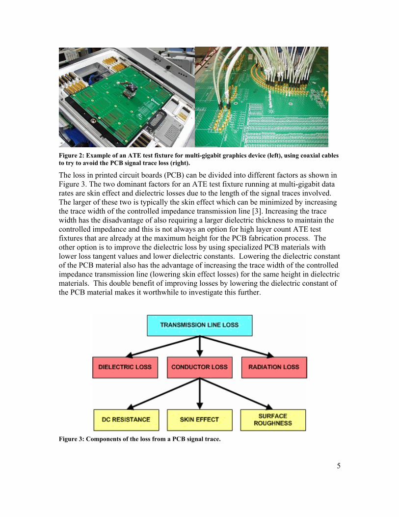
Each of the items in Figure 1 must be optimized and characterized so that the measurement instrumentation on the ATE system accurately measures the real performance of the DUT [1,2]. One of the most problematic items is the signal loss in the ATE test fixture also known as device interface board (DIB) or DUT test fixture. Due to the high pin count of modern systems-on-a-chip SOCs with hundreds of multi-gigabit I/O cells, ATE test fixtures can be very large with signal traces in the 24-50 cm length range (depending on the ATE platform and application). The left side of Figure 2 shows a picture of an ATE test fixture for a device with multiple I/O cells in the 6 Gbps range docked to an ATE system.
5
Figure 2: Example of an ATE test fixture for multi-gigabit graphics device (left), using coaxial cables to try to avoid the PCB signal trace loss (right).
The loss in printed circuit boards (PCB) can be divided into different factors as shown in Figure 3. The two dominant factors for an ATE test fixture running at multi-gigabit data rates are skin effect and dielectric losses due to the length of the signal traces involved. The larger of these two is typically the skin effect which can be minimized by increasing the trace width of the controlled impedance transmission line [3]. Increasing the trace width has the disadvantage of also requiring a larger dielectric thickness to maintain the controlled impedance and this is not always an option for high layer count ATE test fixtures that are already at the maximum height for the PCB fabrication process. The other option is to improve the dielectric loss by using specialized PCB materials with lower loss tangent values and lower dielectric constants. Lowering the dielectric constant of the PCB material also has the advantage of increasing the trace width of the controlled impedance transmission line (lowering skin effect losses) for the same height in dielectric materials. This double benefit of improving losses by lowering the dielectric constant of the PCB material makes it worthwhile to investigate this further.
Figure 3: Components of the loss from a PCB signal trace.
6
In this paper we will concentrate on the dielectric loss for ATE test fixtures by comparing several dielectric materials available in the industry including new advancements in Teflon® based dielectric materials for multi-layer applications. We will start with an introduction to dielectric materials and the challenges they present followed by the latest in low dielectric constant materials for multi-layer PCBs. We will then present several experimental results at 10, 20, and 43 Gbps with an ATE test fixture and show how equalization addresses the remaining test fixture loss challenge after an appropriate choice of dielectric material and trace geometry. The paper will conclude with an evaluation of the benefits of a lower dielectric constant PCB material for a real PCB stack-up of a high density ATE test fixture. The results will clearly show the ability of PCB materials to extend the data rate range of ATE test fixtures beyond 10 Gbps and improve the performance of existing high density designs. Dielectric Materials for ATE Test Fixtures ATE test fixture PCBs including probe cards for wafer sort or test fixtures with sockets for packaged semiconductor device testing tend to be thick (200-300 mil) multilayer PCBs that can include as many as 56 layers of circuitry The size can be as large as 22 inches by 17 inches (55 cm by 43 cm). This is similar to large format telecom backpanels with regard to length, width, and thickness and they face the same signal integrity challenges that these characteristics present. The multiple layers of an ATE test fixture accommodate a variety of routing needs including power planes for low impedance, separation of analog and digital circuitry, and high-speed controlled impedance. A multi-layer PCB is typically limited to around 250 mils in thickness due to manufacturing restrictions. As PCB thicknesses increase beyond 250 mils the PCB manufacturer is faced with the challenge of layer to layer registration, straight drilling, and the plating difficulties of higher aspect ratio plated through holes while trying to maintain the same feature tolerances as a thinner board. These problems are exacerbated as designers try to squeeze more and more transmission lines onto a PCB by using smaller drilled holes, smaller pads, and smaller spaces between signals. Adding additional signals to a design without increasing the total PCB thickness requires that a designer either reduce the thickness of the individual dielectric layers or increase the density of routing on an individual layer by reducing the width of the existing copper traces, the diameters of the drilled holes and the corresponding pads. Squeezing additional transmission lines onto the same dielectric layers ultimately leads to a more complex PCB to design and manufacture with tighter tolerances on layer to layer registration and drilling accuracy. The drive for densification has led to some creative fabrication techniques such as flip drilling on a PCB, where half the hole is drilled from the top and the other half from the bottom in order to maintain the required drill registration of a via. Reducing the layer thickness while using the same PCB material or increasing the routing density on a layer to accommodate more signals both have the adverse affect of reducing trace width and increasing signal losses. An alternate solution is to reduce the layer
7
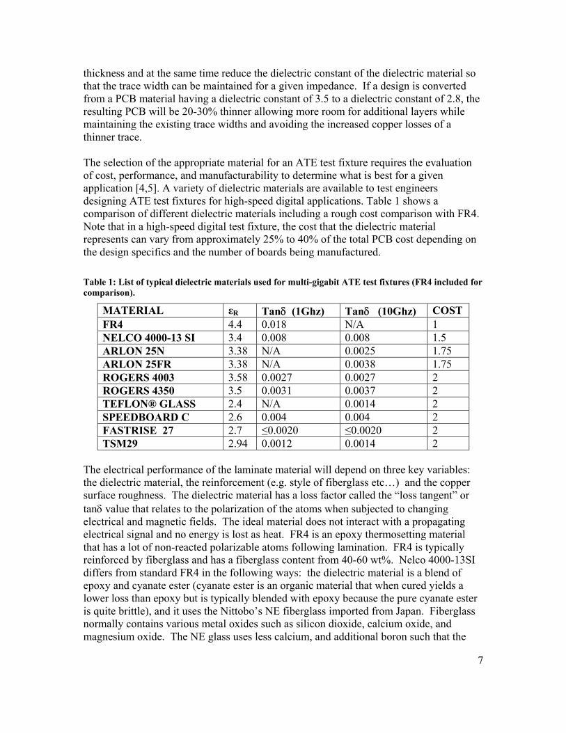
thickness and at the same time reduce the dielectric constant of the dielectric material so that the trace width can be maintained for a given impedance. If a design is converted from a PCB material having a dielectric constant of 3.5 to a dielectric constant of 2.8, the resulting PCB will be 20-30% thinner allowing more room for additional layers while maintaining the existing trace widths and avoiding the increased copper losses of a thinner trace. The selection of the appropriate material for an ATE test fixture requires the evaluation of cost, performance, and manufacturability to determine what is best for a given application [4,5]. A variety of dielectric materials are available to test engineers designing ATE test fixtures for high-speed digital applications. Table 1 shows a comparison of different dielectric materials including a rough cost comparison with FR4. Note that in a high-speed digital test fixture, the cost that the dielectric material represents can vary from approximately 25% to 40% of the total PCB cost depending on the design specifics and the number of boards being manufactured. Table 1: List of typical dielectric materials used for multi-gigabit ATE test fixtures (FR4 included for comparison).
The electrical performance of the laminate material will depend on three key variables: the dielectric material, the reinforcement (e.g. style of fiberglass etc…) and the copper surface roughness. The dielectric material has a loss factor called the “loss tangent” or tanδ value that relates to the polarization of the atoms when subjected to changing electrical and magnetic fields. The ideal material does not interact with a propagating electrical signal and no energy is lost as heat. FR4 is an epoxy thermosetting material that has a lot of non-reacted polarizable atoms following lamination. FR4 is typically reinforced by fiberglass and has a fiberglass content from 40-60 wt%. Nelco 4000-13SI differs from standard FR4 in the following ways: the dielectric material is a blend of epoxy and cyanate ester (cyanate ester is an organic material that when cured yields a lower loss than epoxy but is typically blended with epoxy because the pure cyanate ester is quite brittle), and it uses the Nittobo’s NE fiberglass imported from Japan. Fiberglass normally contains various metal oxides such as silicon dioxide, calcium oxide, and magnesium oxide. The NE glass uses less calcium, and additional boron such that the
8
fiberglass has a reduced dielectric constant (4.4 vs. 6.4 of the E glass used in FR4) and a reduced dissipation factor (0.0035 vs. 0.0067 at 10 GHz). The 25FR, 25N, 4003 and the 4350 are all dielectric materials based on polybutadiene, chemically not very different from natural rubber. The rubber based laminate materials have surprisingly good electrical properties at low temperatures but are prone to oxidation (yellowing in color) and a doubling of their loss tangent when exposed to air at temperatures over 150C. This oxidation at higher temperatures also reduces the strength of the copper adhesion to the material and can be a problem for rework of PCB assemblies. The 25FR and the 4350 are flame retarded versions of silica filled rubber whereas the 4003 and 25N has no flame retardant. The silica filled rubber is typically reinforced with a standard E-glass type 1080 or 106 fiberglass. Simple polytetrafluoroethylene (PTFE) laminates consist of Teflon® and woven fiberglass. These materials tend to suffer from PCB fabrication problems of poor drilling and too much material movement which can cause significant problems on a high layer count ATE test fixture. Ceramic filled PTFE composites are a dramatic improvement relative to simple PTFE-fiberglass composites. PTFE laminates with a high loading of micro-dispersed ceramic yield a much higher quality drilled hole and have less z-axis expansion. The electrical properties of PTFE are stable at higher temperatures and not susceptible to oxidation. For these reasons ceramic filled PTFE laminates are a staple of military designs. TSM29 is a ceramic filled PTFE composite containing a very low glass content (9 wt%). Speedboard C is based on a PTFE film that has been stretched in the x and y directions causing the PTFE to fibrillate and form a porous spider web like structure. The non-reinforced web is then impregnated with ceramic filled organic thermosetting resins. Its biggest advantage is that it has a high degree of flow to fill the gaps between copper features. However, this high degree of flow can also be a disadvantage for high layer count ATE test fixtures where the thick PCB requires registration over many layers and predictable movement of the core materials and prepregs is required. The choice of reinforcement has a lot of implications to the electrical and mechanical properties of the composite. Various authors have published papers in the last few years describing the effects of fiberglass on delay differences or skew between same length traces on a PCB [6,7]. Fiberglass in the as woven state (Figure 4) can have some degree of weave distortion before impregnation.
9
Figure 4: Fiberglass in a woven state showing the flattened fill yarns in the vertical direction and the rod like warp yarns in the horizontal direction.
The basic challenge with fiberglass is that its dielectric constant of 6.4 is a poor match to the 3.2-3.8 permitivity for an epoxy or 2.1 for PTFE. The result is that the propagation velocity along a copper transmission line will speed up or slow down depending on how it is routed over the underlying fiberglass. In a source synchronous type interface application, the variation in signal speed in each lane of the bus can lead to setup and hold failures. In applications using differential signals the skew in propagation time between the two signal traces can cause mode conversion which degrades the desired signal. One author suggests using a fiberglass having a tremendous amount of fiberglass such that there are no windows. This will eliminate the dramatic impedance fluctuations when measured with a TDR but that solution suggests using composites with a high density of very lossy fiberglass. For lossy dielectric materials like FR4, a high fiberglass content can actually lower the overall dissipation factor. For high performance materials like PTFE, introducing a high content of lossy fiberglass is a very unattractive option. Flat fiberglass weaves are fiberglass structures where the fill yarns have been spread out to look flat and close the windows. However, the warp yarns are preserved as tight rods so it is a partial solution and moreover, one is still left with lossy fiberglass. Elimination of fiberglass reduces the intra-pair electrical skew associated with fiberglass and it also eliminates a higher loss component (0.0067 tanδ at 10 GHz). Discussion of using non-reinforced materials has to be divided into two topics, as a prepreg material and as a core material. Manufacturing non-reinforced materials puts a greater burden on the laminate supplier because non-reinforced materials have little mechanical strength. Careful attention must be paid to web handling equipment so as not to stretch, wrinkle or distort the composites. At the PCB fabricator the non-reinforced core material is difficult to handle. Depending on the thickness of the non-reinforced core, handling non-woven material from some vendors can be the equivalent of handling chewing gum. The PCB fabricator has the added complexity of print and etching a delicate laminate and maintaining registration during lamination. The non-reinforced prepreg on the other hand is relatively easy for the fabricator to handle as it only has one process step where it is interleaved between core materials prior to lamination. The authors at this time have only investigated the combination of a non-reinforced prepreg with reinforced core material.
10
The choice of copper for a laminate is a balance between copper adhesion for mechanical strength and copper conductive losses for electrical performance. Figure 5 shows the microstrip insertion loss of a laminate measured with various copper types.
Figure 5: Insertion loss of a laminate measured with various copper types for a dielectric thickness of 16 mil (DT) and a 37 mil trace width (TW).
The worst performing copper has a surface roughness of 5.6 microns (Rz). Generally speaking, the lighter the copper weight, the less surface roughness. Reverse treated half ounce copper, for example, is a better choice than reverse treated 1 ounce. Figure 6 shows a photomicrograph of the surface roughness of the copper used on the Rogers 4350B series of laminates.
Figure 6: Photomicrograph of the copper surface roughness used in Rogers 4350 series of laminates.
Outer-layer copper adhesion is important to prevent the surface traces from losing adhesion to the laminate. On the inner layers, designers have to consider the copper losses due to the rough copper treatment from the material supplier on one side and on the reverse side of the copper the additional inner-layer copper treatment that a fabricator will add to copper to ensure layer to layer adhesion, known in the art as a metal oxide or alternative oxide treatment.
11
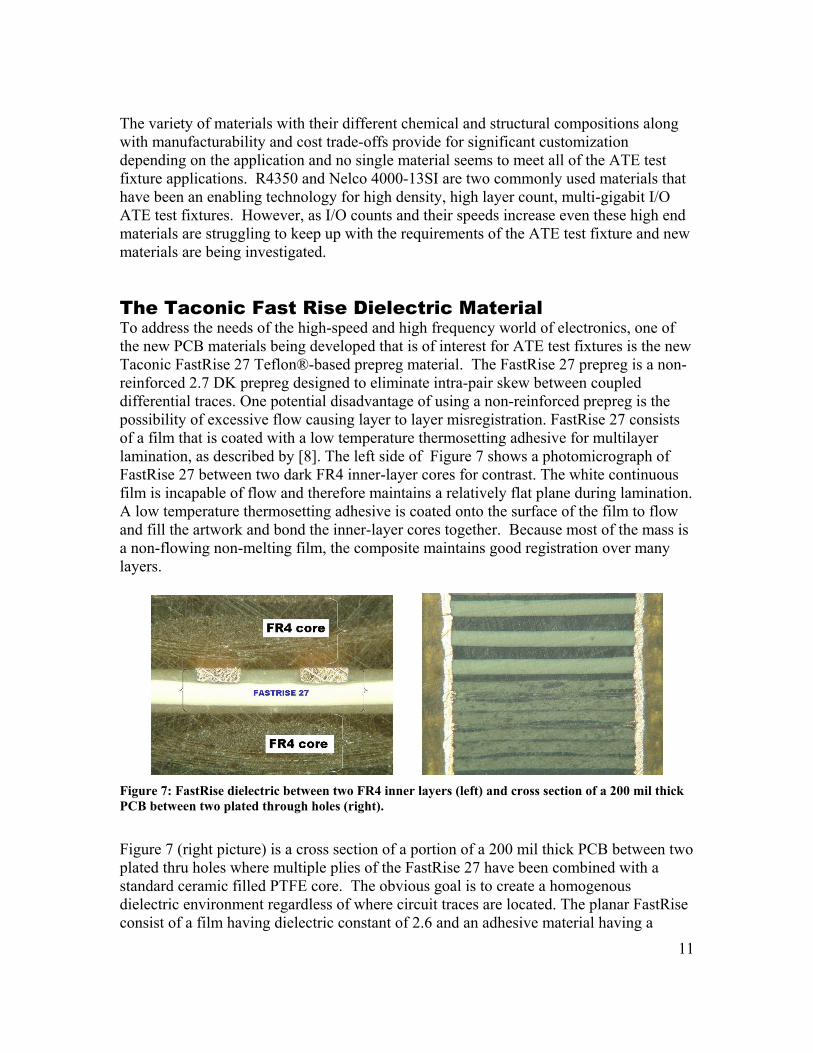
The variety of materials with their different chemical and structural compositions along with manufacturability and cost trade-offs provide for significant customization depending on the application and no single material seems to meet all of the ATE test fixture applications. R4350 and Nelco 4000-13SI are two commonly used materials that have been an enabling technology for high density, high layer count, multi-gigabit I/O ATE test fixtures. However, as I/O counts and their speeds increase even these high end materials are struggling to keep up with the requirements of the ATE test fixture and new materials are being investigated. The Taconic Fast Rise Dielectric Material To address the needs of the high-speed and high frequency world of electronics, one of the new PCB materials being developed that is of interest for ATE test fixtures is the new Taconic FastRise 27 Teflon®-based prepreg material. The FastRise 27 prepreg is a non-reinforced 2.7 DK prepreg designed to eliminate intra-pair skew between coupled differential traces. One potential disadvantage of using a non-reinforced prepreg is the possibility of excessive flow causing layer to layer misregistration. FastRise 27 consists of a film that is coated with a low temperature thermosetting adhesive for multilayer lamination, as described by [8]. The left side of Figure 7 shows a photomicrograph of FastRise 27 between two dark FR4 inner-layer cores for contrast. The white continuous film is incapable of flow and therefore maintains a relatively flat plane during lamination. A low temperature thermosetting adhesive is coated onto the surface of the film to flow and fill the artwork and bond the inner-layer cores together. Because most of the mass is a non-flowing non-melting film, the composite maintains good registration over many layers.
Figure 7: FastRise dielectric between two FR4 inner layers (left) and cross section of a 200 mil thick PCB between two plated through holes (right).
Figure 7 (right picture) is a cross section of a portion of a 200 mil thick PCB between two plated thru holes where multiple plies of the FastRise 27 have been combined with a standard ceramic filled PTFE core. The obvious goal is to create a homogenous dielectric environment regardless of where circuit traces are located. The planar FastRise consist of a film having dielectric constant of 2.6 and an adhesive material having a
12
dielectric constant of 2.8 such that film and adhesives are well matched with regards to permittivity. The primary benefits to the designer are first, a low 2.7 dielectric constant allowing the designer to reduce dielectric thicknesses while maintaining trace widths, second, a very homogeneous dielectric material eliminating skew variations and third the lowest loss thermosetting prepreg commercially available.
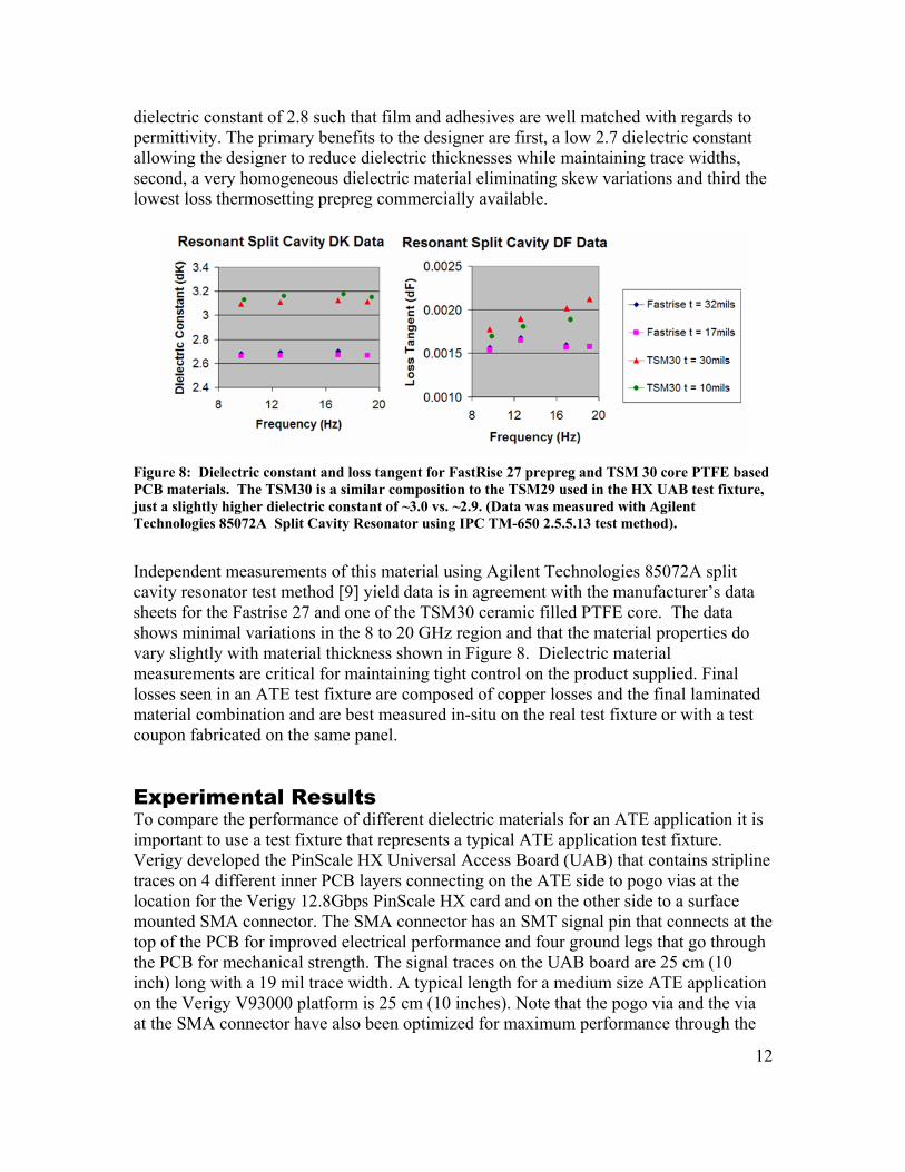
Figure 8: Dielectric constant and loss tangent for FastRise 27 prepreg and TSM 30 core PTFE based PCB materials. The TSM30 is a similar composition to the TSM29 used in the HX UAB test fixture, just a slightly higher dielectric constant of ~3.0 vs. ~2.9. (Data was measured with Agilent Technologies 85072A Split Cavity Resonator using IPC TM-650 2.5.5.13 test method).
Independent measurements of this material using Agilent Technologies 85072A split cavity resonator test method [9] yield data is in agreement with the manufacturer’s data sheets for the Fastrise 27 and one of the TSM30 ceramic filled PTFE core. The data shows minimal variations in the 8 to 20 GHz region and that the material properties do vary slightly with material thickness shown in Figure 8. Dielectric material measurements are critical for maintaining tight control on the product supplied. Final losses seen in an ATE test fixture are composed of copper losses and the final laminated material combination and are best measured in-situ on the real test fixture or with a test coupon fabricated on the same panel. Experimental Results To compare the performance of different dielectric materials for an ATE application it is important to use a test fixture that represents a typical ATE application test fixture. Verigy developed the PinScale HX Universal Access Board (UAB) that contains stripline traces on 4 different inner PCB layers connecting on the ATE side to pogo vias at the location for the Verigy 12.8Gbps PinScale HX card and on the other side to a surface mounted SMA connector. The SMA connector has an SMT signal pin that connects at the top of the PCB for improved electrical performance and four ground legs that go through the PCB for mechanical strength. The signal traces on the UAB board are 25 cm (10 inch) long with a 19 mil trace width. A typical length for a medium size ATE application on the Verigy V93000 platform is 25 cm (10 inches). Note that the pogo via and the via at the SMA connector have also been optimized for maximum performance through the
13
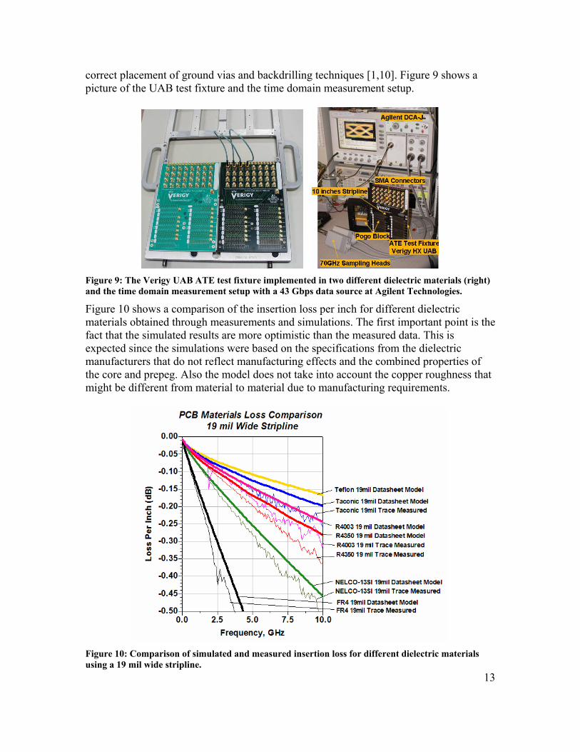
correct placement of ground vias and backdrilling techniques [1,10]. Figure 9 shows a picture of the UAB test fixture and the time domain measurement setup.
Figure 9: The Verigy UAB ATE test fixture implemented in two different dielectric materials (right) and the time domain measurement setup with a 43 Gbps data source at Agilent Technologies.
Figure 10 shows a comparison of the insertion loss per inch for different dielectric materials obtained through measurements and simulations. The first important point is the fact that the simulated results are more optimistic than the measured data. This is expected since the simulations were based on the specifications from the dielectric manufacturers that do not reflect manufacturing effects and the combined properties of the core and prepeg. Also the model does not take into account the copper roughness that might be different from material to material due to manufacturing requirements.
Figure 10: Comparison of simulated and measured insertion loss for different dielectric materials using a 19 mil wide stripline.
14
This dependence on the as-fabricated laminate for the trace loss can also vary between fabrication vendors since the details of surface treatments and lamination processes are often proprietary and not directly described on the PCB fabrication drawing. This should always be checked when changing fabrication vendors on high-speed digital designs. The data for two particular vendors using R4350 agreed quite well for the material losses, but showed significant differences in the performance of the via transitions which affects the losses above 10 GHz (see Figure 11). Comparing the stripline loss performance from multiple layers on the same board from one vendor (right side of Figure 11) indicates that although the via transition has some variations at the higher frequencies, the variations are not as large as that seen between Vendor A and Vendor B (left side of Figure 11). This demonstrates how critical the connector and via topology are for transitioning into and out of an ATE test fixture PCB if one wants to achieve the full benefit of the lower loss materials at higher data rates.
Figure 11: Measured data for the ATE HX UAB test fixture comparing the 10 inch stripline loss for two vendors (left) and for 4 different layers within one vendors board (right).
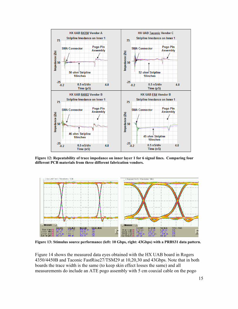
One can also look at the quality of the transmission line impedance as a function of distance along the trace using time domain analysis as shown in Figure 12. The data for four different board materials from three different vendors shows that 50 Ohm impedances with +/-5% tolerances are reasonable to expect for the higher performance materials. To compare the time domain performance on the UAB test fixture manufactured with the Rogers 4350 and Taconic FastRise dielectric, a 6.5 pS 10-90 rise time driver was used as a time domain stimulus source for data eye measurements up to 43 Gbps. The data eyes were measured using an Agilent Technologies DCA-J with a precision time base and a 70 GHz remote sampling head. Figure 13 shows the performance of the stimulus source measured at its output with a PRBS31 data pattern at 10 Gbps and 43 Gbps.
15
Figure 12: Repeatability of trace impedance on inner layer 1 for 6 signal lines. Comparing four different PCB materials from three different fabrication vendors.
Figure 13: Stimulus source performance (left: 10 Gbps, right: 43Gbps) with a PRBS31 data pattern.
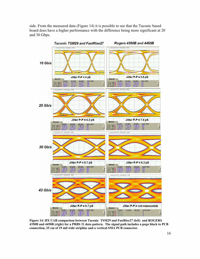
Figure 14 shows the measured data eyes obtained with the HX UAB board in Rogers 4350/4450B and Taconic FastRise27/TSM29 at 10,20,30 and 43Gbps. Note that in both boards the trace width is the same (to keep skin effect losses the same) and all measurements do include an ATE pogo assembly with 5 cm coaxial cable on the pogo
16
side. From the measured data (Figure 14) it is possible to see that the Taconic based board does have a higher performance with the difference being more significant at 20 and 30 Gbps.
Figure 14: HX UAB comparison between Taconic TSM29 and FastRise27 (left) and ROGERS 4350B and 4450B (right) for a PRBS 31 data pattern. The signal path includes a pogo block to PCB connection, 25 cm of 19 mil wide stripline and a vertical SMA PCB connector.
17
This can again be seen in Figure 14 where the measured data eye height comparison is displayed in a graph.
Figure 15: Comparison of the data eye height at different data rates between the UAB test fixture in Rogers 4350 and Taconic Fast Rise for a PRBS31 data pattern
This graph shows the interesting fact that for lower data rates, the loss is mainly dominated by the skin effect. For higher data rates the dielectric loss becomes a more significant contributor to performance and the dielectric loss difference between the Taconic and Rogers materials becomes a factor. At 43 Gbps the transitions on the board become the main performance bottleneck and the eye amplitude is dropping rapidly. Remember that all measurements include the ATE pogo assembly and the SMA connector. Here the Taconic material still has a measurable eye opening while the R4350 is almost closed. Equalization to the Rescue The previous sections presented the performance of an evaluation ATE test fixture with different dielectric materials showing a slightly open data eye even at 43 Gbps. Of course the data eye does not have the needed performance for a test and measurement application at those speeds, but with the correct choice of dielectric material, trace geometry and interconnect technology there is the possibility of using equalization to achieve the needed performance [11]. Figure 16 shows the basics of equalization using a passive equalization filter approach as an example [12,13].
18
Figure 16: Basics of signal path loss equalization through a passive equalization filter.
The objective of equalization is to remove the frequency-dependent loss that is inherent to any real PCB. To demonstrate the possible improvements that equalization can provide we used the Verigy V93000 PinScale HX ATE pin electronics card that includes integrated equalization that is able to achieve a 12.8 Gbps data rate. The equalizer on the Verigy PinScale HX card is a passive equalizer with a fixed response tailored for a typical text fixture. Figure 17 shows the measured power spectrum at the driver output on a special bench setup. One curve is at the end of the test fixture with equalization and another curve is at the end of the test fixture without equalization for the ATE HX UAB test fixture using the Rogers 4350 dielectric material. From Figure 17 it is possible to observe that the equalization compensates for the low-pass effect which the test fixture creates on the data signal spectrum. In the presented case the equalizer is able to get the data spectrum closer to the original one measured at the driver output.
Figure 17: Power spectrum of a 12.8Gbps PRBS31 data signal at the driver output and measured after 10 inch of a 19 mil stripline in Rogers 4350 dielectric material with and without equalization.
19
This same phenomenon can also be seen in Figure 18 which shows the measured data eyes at 12.8 Gbps with and without equalization. Clearly for data rates above 10 Gbps, like 43 Gbps, the same approach has to be taken and equalization must be used to compensate for the frequency dependence of the trace loss.
Figure 18: Comparison of the data eye at the output of the ATE test fixture with and without equalization using the Rogers 4350 dielectric materials with a PRBS 31 data pattern at 12.8 Gbps.
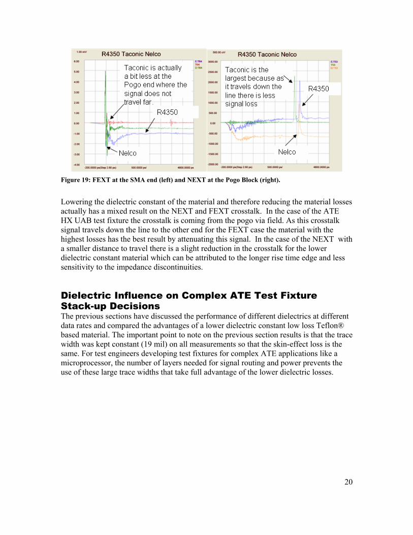
NEXT/FEXT Crosstalk Variations with PCB Materials The selection of dielectric material not only impacts the signal performance in terms of its effect on the signal trace loss but can also have an impact on crosstalk in an ATE test fixture. This is especially true given the fast rise-times that are a result of the higher data rates of modern I/O cells. Telecommunication systems running at 10 Gbps can have 30 pS rise times which is equivalent to a distance of 171 mils in FR4 at a dielectric constant of 4.4 and a distance of 210 mils in Taconic material with an average dielectric constant of 2.9. The shorter the length of the rise-time edge, the more sensitive it will be to the feature variations on the PCB. The sensitivity is due to the fact that the voltage will vary dramatically across this distance and any feature on the order of the length of the rise time edge or larger will require impedance matching to prevent reflections. Lowering the dielectric constant increases the rise time length in the material which can reduce the amplitude of the reflections, however, at the same time the lower losses of the material means that the reflections are attenuated less as they travel along the signal path. Typically the worst crosstalk offenders in ATE test fixtures are the pogo vias [14] and the vias to the socket. Figure 19 shows the NEXT and FEXT crosstalk results for the UAB boards manufactured in three different materials (NELCO 4000-13 SI, Rogers 4350 and Taconic TSM 29 with FastRise 27 prepreg).
20
Figure 19: FEXT at the SMA end (left) and NEXT at the Pogo Block (right).
Lowering the dielectric constant of the material and therefore reducing the material losses actually has a mixed result on the NEXT and FEXT crosstalk. In the case of the ATE HX UAB test fixture the crosstalk is coming from the pogo via field. As this crosstalk signal travels down the line to the other end for the FEXT case the material with the highest losses has the best result by attenuating this signal. In the case of the NEXT with a smaller distance to travel there is a slight reduction in the crosstalk for the lower dielectric constant material which can be attributed to the longer rise time edge and less sensitivity to the impedance discontinuities. Dielectric Influence on Complex ATE Test Fixture Stack-up Decisions The previous sections have discussed the performance of different dielectrics at different data rates and compared the advantages of a lower dielectric constant low loss Teflon® based material. The important point to note on the previous section results is that the trace width was kept constant (19 mil) on all measurements so that the skin-effect loss is the same. For test engineers developing test fixtures for complex ATE applications like a microprocessor, the number of layers needed for signal routing and power prevents the use of these large trace widths that take full advantage of the lower dielectric losses.
21
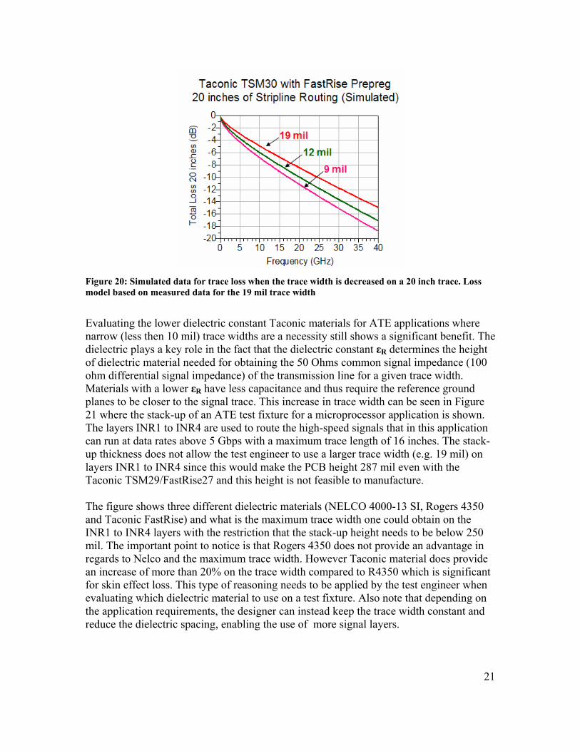
Figure 20: Simulated data for trace loss when the trace width is decreased on a 20 inch trace. Loss model based on measured data for the 19 mil trace width
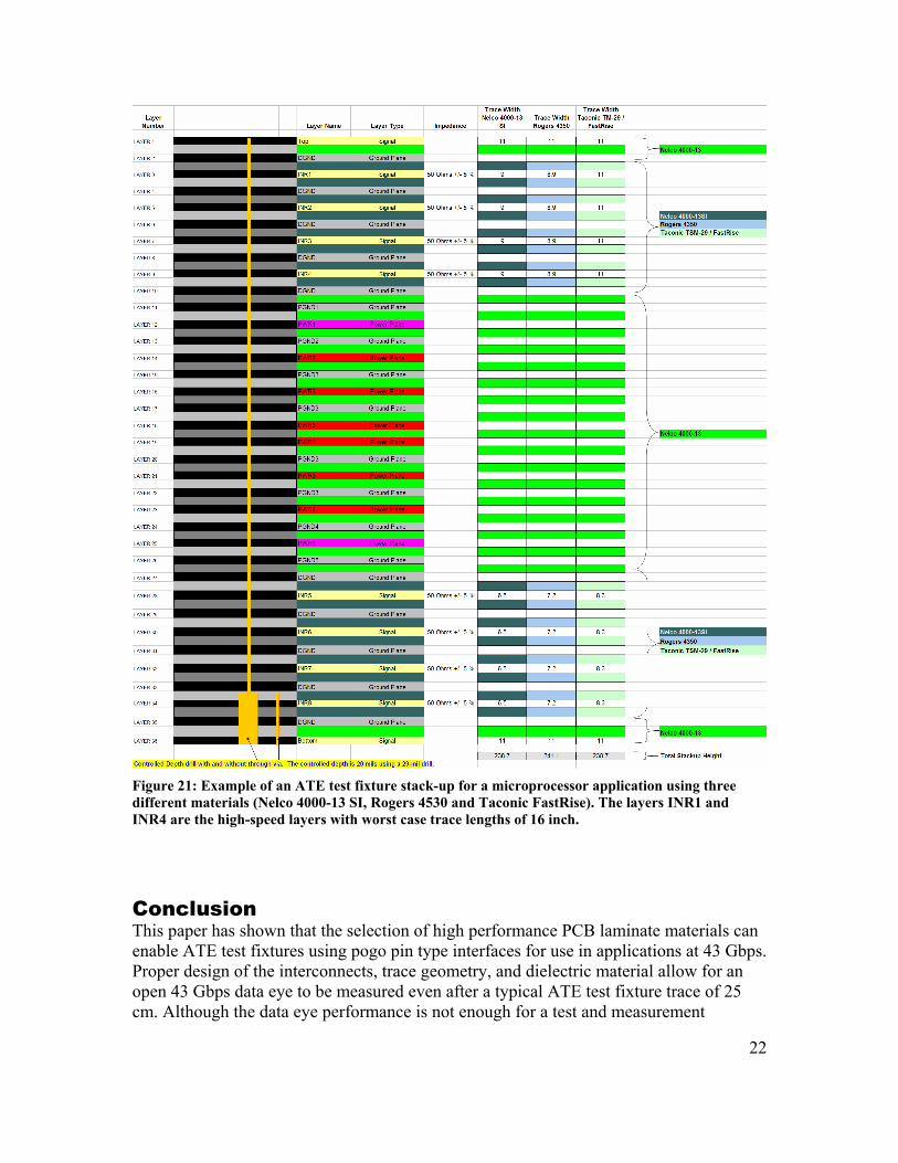
Evaluating the lower dielectric constant Taconic materials for ATE applications where narrow (less then 10 mil) trace widths are a necessity still shows a significant benefit. The dielectric plays a key role in the fact that the dielectric constant εR determines the height of dielectric material needed for obtaining the 50 Ohms common signal impedance (100 ohm differential signal impedance) of the transmission line for a given trace width. Materials with a lower εR have less capacitance and thus require the reference ground planes to be closer to the signal trace. This increase in trace width can be seen in Figure 21 where the stack-up of an ATE test fixture for a microprocessor application is shown. The layers INR1 to INR4 are used to route the high-speed signals that in this application can run at data rates above 5 Gbps with a maximum trace length of 16 inches. The stack-up thickness does not allow the test engineer to use a larger trace width (e.g. 19 mil) on layers INR1 to INR4 since this would make the PCB height 287 mil even with the Taconic TSM29/FastRise27 and this height is not feasible to manufacture. The figure shows three different dielectric materials (NELCO 4000-13 SI, Rogers 4350 and Taconic FastRise) and what is the maximum trace width one could obtain on the INR1 to INR4 layers with the restriction that the stack-up height needs to be below 250 mil. The important point to notice is that Rogers 4350 does not provide an advantage in regards to Nelco and the maximum trace width. However Taconic material does provide an increase of more than 20% on the trace width compared to R4350 which is significant for skin effect loss. This type of reasoning needs to be applied by the test engineer when evaluating which dielectric material to use on a test fixture. Also note that depending on the application requirements, the designer can instead keep the trace width constant and reduce the dielectric spacing, enabling the use of more signal layers.
22
Figure 21: Example of an ATE test fixture stack-up for a microprocessor application using three different materials (Nelco 4000-13 SI, Rogers 4530 and Taconic FastRise). The layers INR1 and INR4 are the high-speed layers with worst case trace lengths of 16 inch.
Conclusion This paper has shown that the selection of high performance PCB laminate materials can enable ATE test fixtures using pogo pin type interfaces for use in applications at 43 Gbps. Proper design of the interconnects, trace geometry, and dielectric material allow for an open 43 Gbps data eye to be measured even after a typical ATE test fixture trace of 25 cm. Although the data eye performance is not enough for a test and measurement
23
application, the development of appropriate equalization techniques can compensate for this increasing loss with frequency and improve the data eye to meet the needs of an ATE application. It is important to note that equalization does not provide a perfect solution and will have some limits due to the amount of power that the ATE system can give up to increase the equalization strength (increasing pin counts on ATE systems create significant power management challenges). Selecting a lower loss dielectric material will minimize the amount of correction required by the equalizer leaving more power available for the transmitted signals. The results presented in this paper comparing several dielectric materials with a typical ATE test fixture clearly show that available high-end multi-layer dielectric materials provide similar performance at 10 Gbps where losses are still similar in magnitude and are dominated by the skin effect losses. At higher data rates the lower losses of the Taconic materials did show an improved performance when compared to existing high performance materials like Rogers 4350 and Nelco 4000-13SI. Comparison of crosstalk performance shows that FEXT from the pogo via transition can actually be higher with a low loss material where there is less attenuation of the crosstalk, while the NEXT can actually improve due to a reduction in reflections at the pogo via as the wavelength or rise time edge is lengthened by the lower εR value. A lower dielectric constant material also provides an indirect improvement in performance at lower data rates for certain high density ATE applications. When a high density ATE test fixture is limited in layer count due to the maximum stack-up height that can be fabricated then a lower εR value reduces the dielectric height that is required for the high-speed signal layers of a given trace width. This benefit allows the designer to either add more signal layers to improve signal routing or to widen the trace width of the controlled impedance lines to reduce the skin effect losses. It is important to make clear that the full benefits of a lower loss dielectric material can easily be masked by the losses of the via transitions. In the case of the ATE test fixtures measured for this paper it was found that the pogo via and connector via transitions can start degrading performance above 10 Gbps and are the limiting factor at 43 Gbps. So the next challenge to moving the data rates ever higher on an ATE test fixture will be in the area of via transition optimization and tighter fabrication tolerances for repeatable electrical performance. Acknowledgements We would like to acknowledge Altanova for layout and assembly of the measured ATE test fixtures and specifically Don Sionne at Altanova for his contributions to the cost comparisons of PCB materials. We would like to thank Wendell Anderson and Shelly Baglia of Agilent Technologies for their assistance in measuring PCB material properties. We would like to thank Morgan Culver of Agilent Technologies for the use of the fast rise time 43 Gbps bench test system for the time domain measurements.
24
References [1] Jose Moreira, Heidi Barnes al., “PCB Loadboard Design Challenges for Multi-Gigabit Devices in Automated Test Applications,” IEC DesignCon 2006. [2] Masashi Shimanouchi, ”New Paradigm for Signal Paths in ATE Pin Electronics are Needed for Serialcom Device Testing,” Proceedings of the International Test Conference 2002. [3] Jeff Loyer, “Proper PCB Stackup and Trace Geometry Design are Key Elements in the Fight to Lower Losses”, Printed Circuit Design & Manufacture 2006. [4] J. Moreira, H. Barnes, W. Burns, D. Sionne, C. Gutierrez, F. Azeem, “Influence of Dielectric Materials on ATE Test Fixtures for High-Speed Digital Applications“, Proceedings of the Sixth International Kharkov Conference on the Physics and Engineering of Microwave, Millimeter and Submillimeter Waves 2007. [5] Martin W. Jawitz and Michael J. Jawitz,”Materials for Rigid and Flexible Printed Wiring Boards,” CRC Press 2006. [6] Jeff Loyer, Richard Kunze and Xiaoning Ye, “Fiber Weave Effect: Practical Impact Analysis and Mitigation Strategies”, IEC DesignCon 2007. [7] Scott McMorrow and Chris Head, “The Impact of PCB Laminate Weave on the Electrical Performance of Differential Signaling at Multi-gigabit Data Rates”, IEC DesignCon East 2005. [8] Thomas F. McCarthy and David L. Wynants Sr., “Low signal loss bonding ply for multilayer circuit boards”, US patent 6,500,529. [9] “Basics of Measuring the Dielectric Properties of Materials” Agilent Application Note, PN 5989-2589EN. [10] H. Barnes, J. Moreira, H. Ossoinig, M. Wollitzer, T. Schmidt, M. Tsai, “Development of a Pogo Via Design for Multi-Gigabit Interfaces on Automated Test Equipment,” Proceedings of the 2006 Asia-Pacific Microwave Conference. [11] J. Moreira, H. Barnes, H. Kaga, M. Comai, B. Roth, M. Culver, “Beyond 10Gb/s? Challenges of Characterizing Future I/O Interfaces with Automated Test Equipment”. Presented at the 1st IEEE International Workshop on Automated Test Equipment: VISION ATE 2020. [12] Wolfram Humann, “Compensation of Transmission Line Loss for Gbit/s Test on ATEs,” Proceedings of the International Test Conference 2002. [13] Jose Moreira et al., “Passive Equalization of Test Fixture for High-Speed Digital Measurements with Automated Test Equipment,” Proceedings of the 2006 International Design and Test Workshop. [14] B. Szendrenyi, H. Barnes, J. Moreira, M. Wollitzer, T. Schmid and M. Tsai, “Addressing the Broadband Crosstalk Challenges of Pogo Pin Type Interfaces for High-Density High-Speed Digital Applications,” 2007 IEEE International Microwave Symposium.