73
Atomic Force Microscopy Robyn Snow 1
| Date post: | 26-Dec-2015 |
| Category: |
Documents |
| Upload: | georgia-rodgers |
| View: | 218 times |
| Download: | 0 times |
1
Atomic Force Microscopy
Robyn Snow

2https://www.pinterest.com/lictorn/gary-larson-the-far-side
3
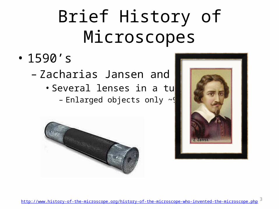
Brief History of Microscopes
• 1590’s – Zacharias Jansen and father
• Several lenses in a tube– Enlarged objects only ~9X
http://www.history-of-the-microscope.org/history-of-the-microscope-who-invented-the-microscope.php
4
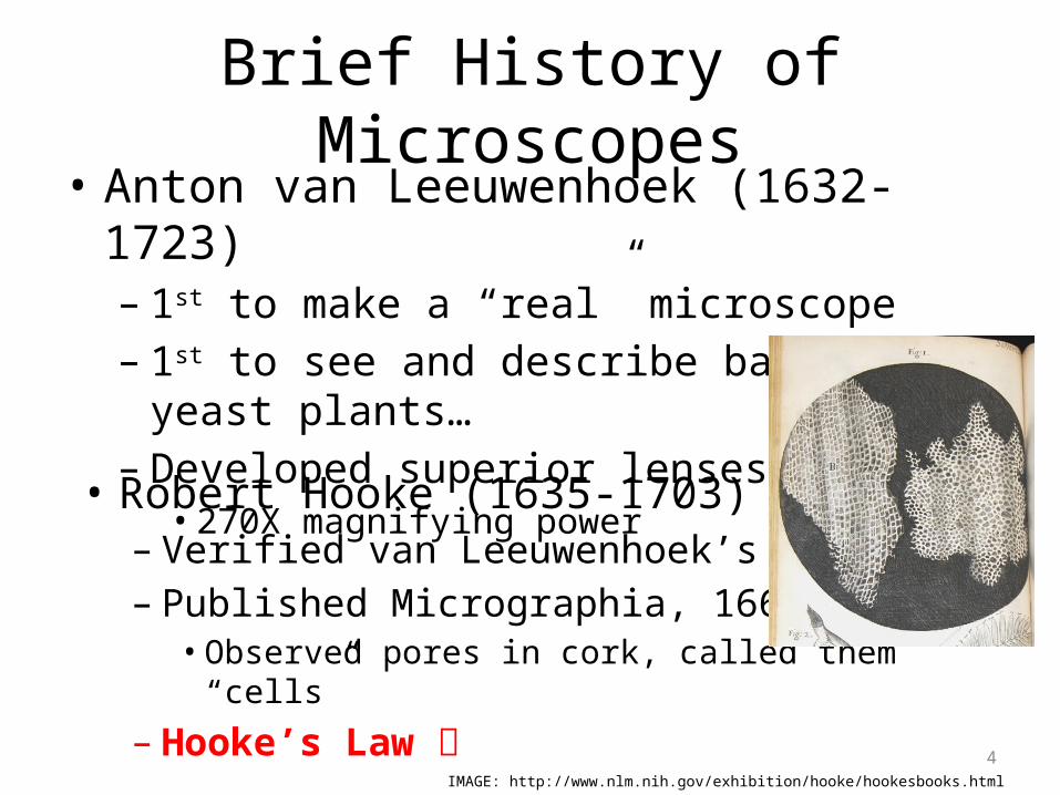
Brief History of Microscopes• Anton van Leeuwenhoek (1632-1723)
– 1st to make a “real” microscope– 1st to see and describe bacteria, yeast plants…– Developed superior lenses
• 270X magnifying power
• Robert Hooke (1635-1703)– Verified van Leeuwenhoek’s work– Published Micrographia, 1665
• Observed pores in cork, called them “cells”
– Hooke’s Law IMAGE: http://www.nlm.nih.gov/exhibition/hooke/hookesbooks.html
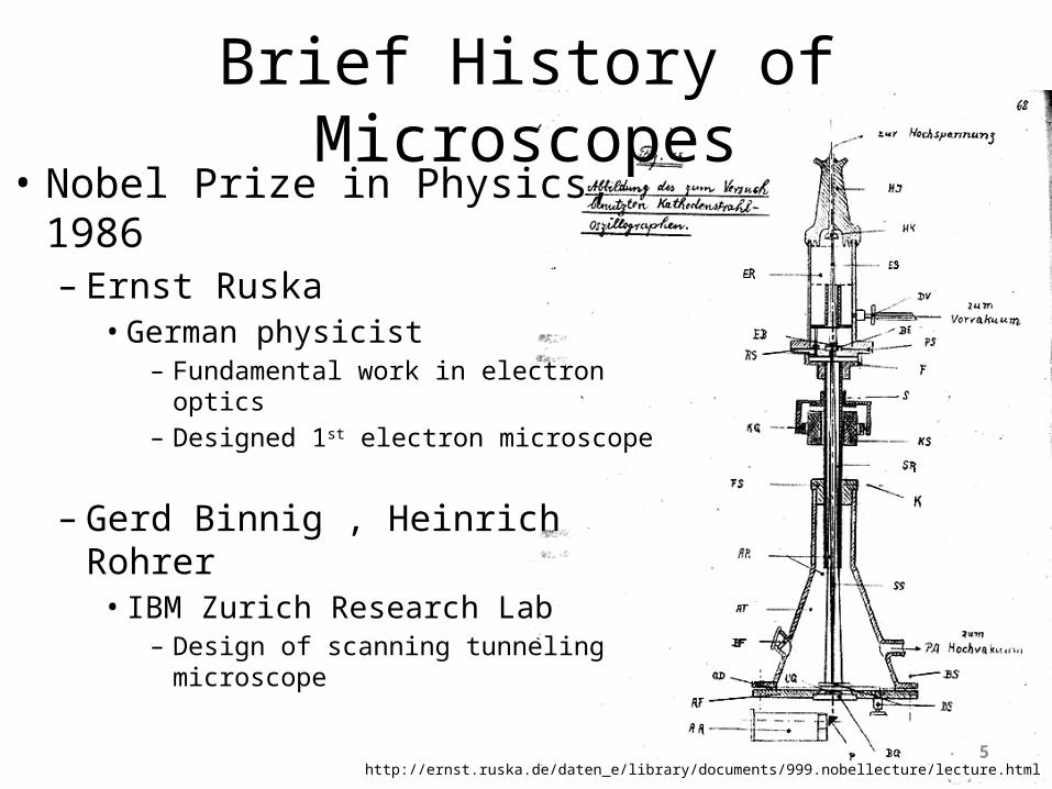
Brief History of Microscopes• Nobel Prize in Physics, 1986
– Ernst Ruska• German physicist
– Fundamental work in electron optics– Designed 1st electron microscope
– Gerd Binnig , Heinrich Rohrer• IBM Zurich Research Lab
– Design of scanning tunneling microscope
5http://ernst.ruska.de/daten_e/library/documents/999.nobellecture/lecture.html

6
General Overview of AFM
• Surface analysis technique– Surface topography– Elasticity– Friction– Magnetic forces– Electrostatic forces

7
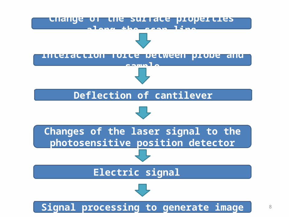
General Operation
– Small probe is scanned across surface – Data from interaction with surface is stored for
each point– Image is displayed as an intensity map, I(x,y) ; I =
parameter sensed by the probe• For AFM, the height of the surface is sensed• LFM, friction• MFM, magnetic fields
8
Interaction force between probe and sample
Deflection of cantilever
Changes of the laser signal to the photosensitive position detector
Electric signal
Signal processing to generate image
Change of the surface properties along the scan line
9
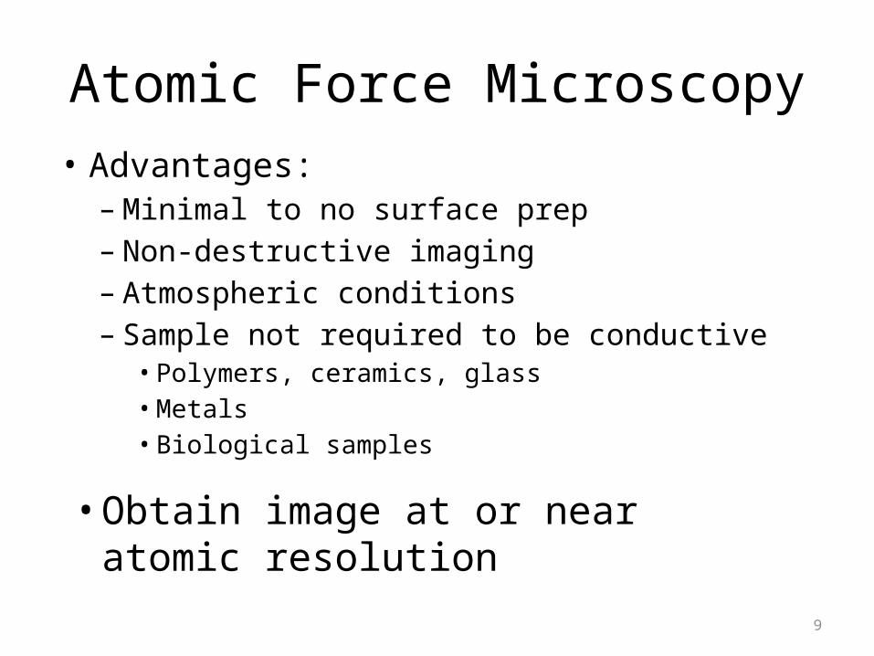
Atomic Force Microscopy
• Obtain image at or near atomic resolution
• Advantages:– Minimal to no surface prep– Non-destructive imaging– Atmospheric conditions– Sample not required to be conductive
• Polymers, ceramics, glass• Metals• Biological samples
10
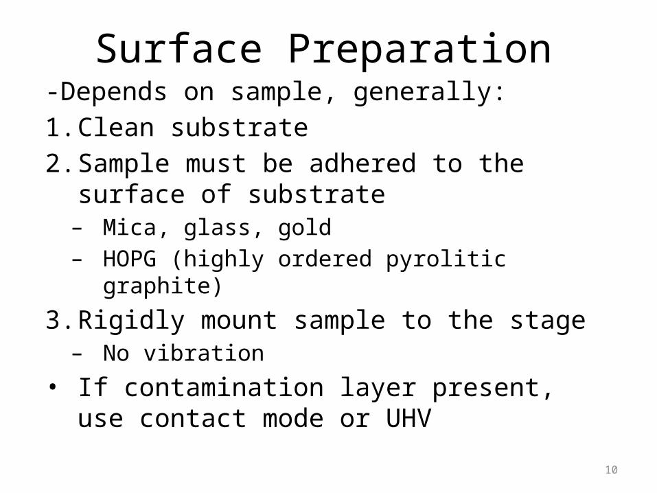
Surface Preparation-Depends on sample, generally:1. Clean substrate2. Sample must be adhered to the surface of
substrate– Mica, glass, gold– HOPG (highly ordered pyrolitic graphite)
3. Rigidly mount sample to the stage– No vibration
• If contamination layer present, use contact mode or UHV

11
Resolution
Vertical Resolution:• Laser intensity noise• Photodiodes noise• Thermal noise of
cantilever• Vertical scanner resolution
<1Å(0.1nm)• Noise: electrical,
mechanical, acoustic
Lateral Resolution
• Lateral resolution ~30nm• Vertical resolution ~0.1nm• Limited to scan areas of 100μm
• Tip sharpness / shape• Scanner resolution in X,Y• Pixelization
– EX: 50μmX 50μm image– Samples/line @512 – Pixel size=0.098 μm =>cannot resolve features smaller than 98nm with 50μm scan size

12
Gold Nanoparticles
http://www.afmworkshop.com/products-main/image-gallery.html#!nanotriangle_pm
http://www.afmworkshop.com/products-main/image-gallery.html#!gold_nanoparticles_100_nm_pm

13
Diagram of Instrument
Probe

14
Probe• Probe: Si or Si3N4
• Only part that contacts sample– Like the “eye” of the instrument– > shape is critical! -> Resolution depends on it
15
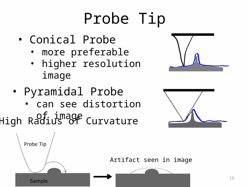
Probe Tip• Conical Probe
• more preferable• higher resolution image
• Pyramidal Probe• can see distortion of image
• High Radius of Curvature
Artifact seen in image

16
Fat-tip Effect: apparent width measured by large tip
x
w
Rtip
RSample
•When Rtip ~ ¼ Rsample, measured width = 2Rsample•Normal tip size, ~ 20 nm or larger.
17
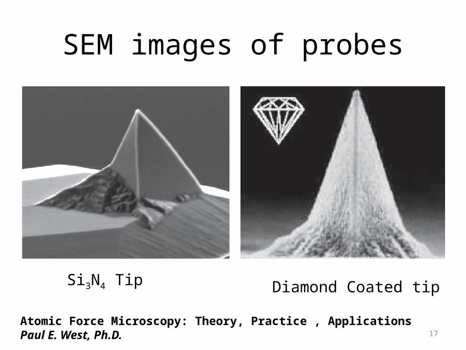
Si3N4 Tip Diamond Coated tip
SEM images of probes
Atomic Force Microscopy: Theory, Practice , ApplicationsPaul E. West, Ph.D.

18
Conical Tip and Cantilever
Silicon Cantilever Length (µm): 225
Res. Frequency (kHz): 28Spring Constant (N/m): 0.1
Tip Radius ~8nmhttp://store.nanoscience.com/store/pc/viewPrd.asp?idproduct=2556&idcategory=4
19
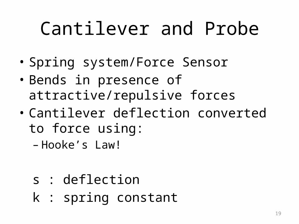
Cantilever and Probe
• Spring system/Force Sensor• Bends in presence of attractive/repulsive
forces• Cantilever deflection converted to force using:
– Hooke’s Law!
s : deflectionk : spring constant
20
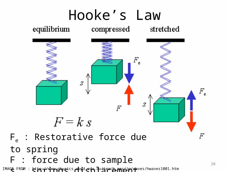
Hooke’s Law
IMAGE FROM : http://www.physics.usyd.edu.au/teach_res/jp/waves/hwaves1001.htm
Fe : Restorative force due to springF : force due to samples : springs displacement from equilibrium
21
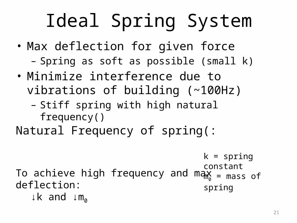
Ideal Spring System• Max deflection for given force
– Spring as soft as possible (small k)
• Minimize interference due to vibrations of building (~100Hz)– Stiff spring with high natural frequency()
Natural Frequency of spring(:
To achieve high frequency and max deflection:↓k and ↓m0
k = spring constantm0 = mass of spring

22
Spring Constant, k
• For a rectangular cantilever:
𝑡
𝑙
𝑤
• E = Young’s modulus• Measure of stiffness • For Si, E = 1.3*1011N/m2
𝑘=𝐸𝑤𝑡3
4 𝑙3
• Typical values for k : 0.001 to 100 N/m• ~100microns in length , a few microns thick
23
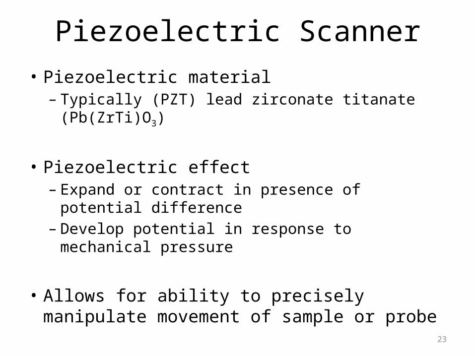
Piezoelectric Scanner• Piezoelectric material
– Typically (PZT) lead zirconate titanate (Pb(ZrTi)O3)
• Piezoelectric effect– Expand or contract in presence of potential
difference– Develop potential in response to mechanical pressure
• Allows for ability to precisely manipulate movement of sample or probe

24
Piezoelectricity
http://www.ytca.com/lead_free_piezoelectric_ceramics
• Polarization in one direction occurs due to applied electric field– Change in length field strength
• ~0.1nm per applied Volt

25

26
Light Lever Sensor• Force Sensor
– Detects changes in height/ deflection based on angle of reflected light

27
Photodetector
A B
D C
• Photosensitive elements (photodiodes)• Photocurrent is produced upon
illumination for each quadrant
• The ratio between the photocurrent from each quadrant determines the relative position of the laser beam
28
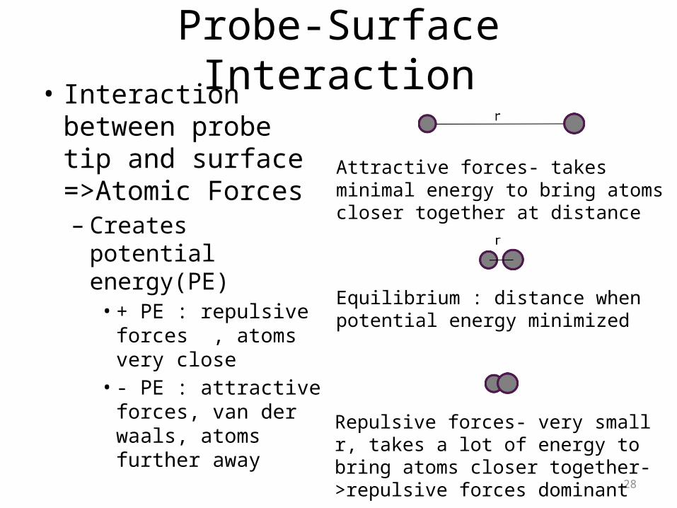
Probe-Surface Interaction• Interaction between
probe tip and surface =>Atomic Forces– Creates potential
energy(PE)• + PE : repulsive
forces , atoms very close
• - PE : attractive forces, van der waals, atoms further away
Attractive forces- takes minimal energy to bring atoms closer together at distance
Equilibrium : distance when potential energy minimized
Repulsive forces- very small r, takes a lot of energy to bring atoms closer together->repulsive forces dominant

29
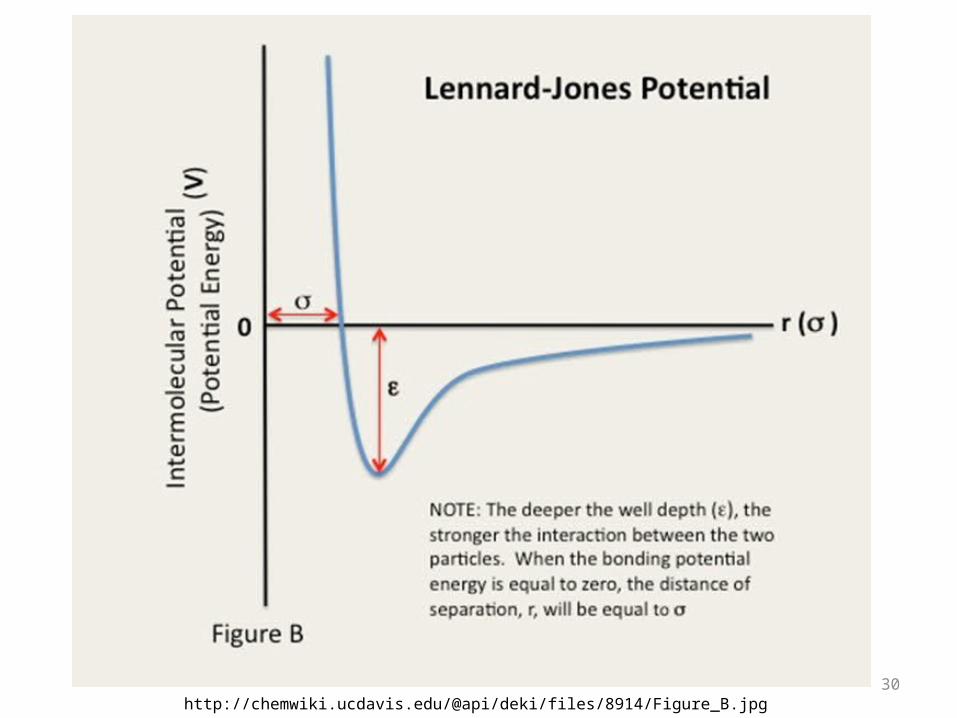
Lennard-Jones Potential (LJP)
• Empirical Model, describes potential energy (V) of interaction between outermost atom of tip and surface atoms
: well depth- measure of strength of attraction : distance at which V is zero (equilibrium)r : distance of separation
30
n
http://chemwiki.ucdavis.edu/@api/deki/files/8914/Figure_B.jpg

31
Van der Waals Forces𝑉 (𝑟 )=4∈[(𝜎𝑟 )
12
−( 𝜎𝑟 )6](𝜎𝑟 )
12
(𝜎𝑟 )6

32
Modes of Imaging
Repulsive
Attractive
Tapping Mode
Non-Contact ModeContact Mode
http://virtual.itg.uiuc.edu/training/AFM_tutorial/
33
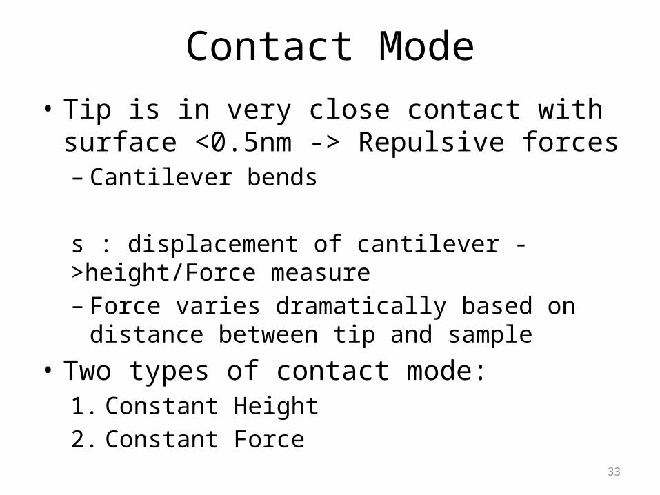
Contact Mode• Tip is in very close contact with surface <0.5nm
-> Repulsive forces– Cantilever bends
s : displacement of cantilever ->height/Force measure– Force varies dramatically based on distance
between tip and sample• Two types of contact mode:
1. Constant Height2. Constant Force

34
Constant Height Contact Mode
• Maintain constant height of sampler– Variations of deflection of lever are recorded as
topography• Deflection ↑ as height of sample ↑• Deflection ↓ as height of sample ↓
• Advantages– Higher scanning speeds– High resolution
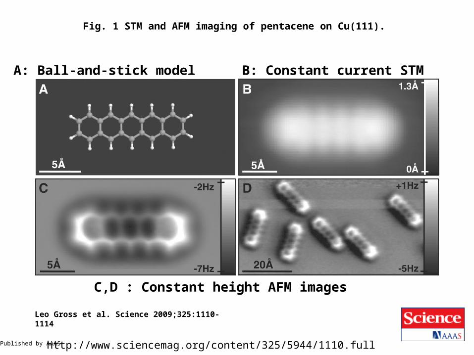
Fig. 1 STM and AFM imaging of pentacene on Cu(111).
Leo Gross et al. Science 2009;325:1110-1114
Published by AAAS
A: Ball-and-stick model B: Constant current STM
C,D : Constant height AFM images
http://www.sciencemag.org/content/325/5944/1110.full

36
Constant Force Contact Mode
• Maintain constant force between tip and sample – Regulate height of sample relative to the tip
• Feedback loop : photodetector and piezoelectric scanner
– Height of sample ↑ , Force ↑, lower height of sample to maintain constant force
• Slower scan speeds• Advantage:
– Can simultaneously measure other characteristics/forces
37
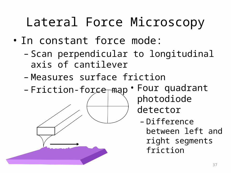
Lateral Force Microscopy• In constant force mode:
– Scan perpendicular to longitudinal axis of cantilever– Measures surface friction – Friction-force map
• Four quadrant photodiode detector– Difference between
left and right segments friction

38
Lateral Deflection
• Magnitude depends on:
– Frictional coefficient of the sample
– Topography of sample surface
– Cantilevers lateral spring constant

39
Lateral Force Spring Constant• Lateral spring constant:
G : shear modulus-measure of elasticityr : length of tip
∆s
Force
𝒘
𝒕
𝒍

40
Lateral Force Calibration
• Calibration of :– normal and lateral forces, F– Photodiode sensitivity, S
• Using reference sample• Normal Force• Lateral Force• lateral calibration factor
– Transforms lateral ΔV ->Friction Force (nN)
41http://www.parkafm.com/images/spmmodes/standard/Lateral-Force-Microscopy-(LFM).pdf
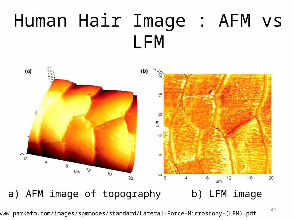
a) AFM image of topography b) LFM image
Human Hair Image : AFM vs LFM
42
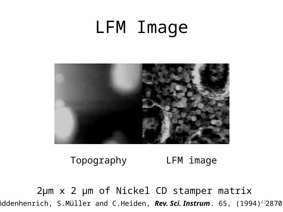
LFM Image
Topography LFM image
2μm x 2 μm of Nickel CD stamper matrixT.Göddenhenrich, S.Müller and C.Heiden, Rev. Sci. Instrum. 65, (1994) 2870
43
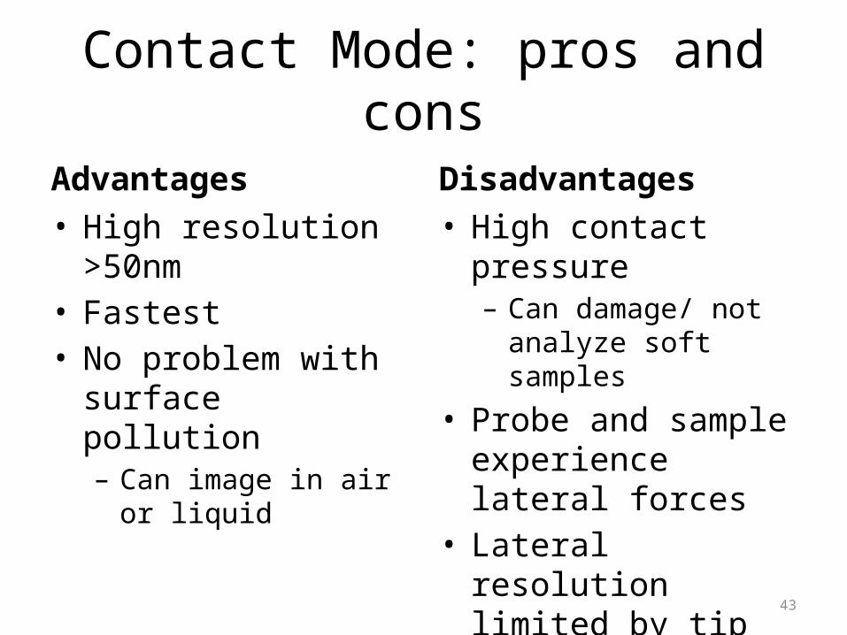
Contact Mode: pros and cons
Advantages• High resolution >50nm• Fastest• No problem with
surface pollution– Can image in air or liquid
Disadvantages• High contact pressure
– Can damage/ not analyze soft samples
• Probe and sample experience lateral forces
• Lateral resolution limited by tip sharpness
• Lowers lifetime of tip

44
Non-contact Mode• Lever(spring) oscillates close to its resonance
frequency from driving piezo– => Use z-piezo to vibrate the cantilever near its
resonant frequency
• Forces shift this oscillation
tip-sample distance of ~5-10nm

45
Z-drive Piezo for Non-contact AFM
• Informs feedback loop of motion of tip/cantilever:• Frequency• Amplitude
• Allows for frequency modulation(FM-AFM) or amplitude modulation (AM-AFM/tapping mode)
46
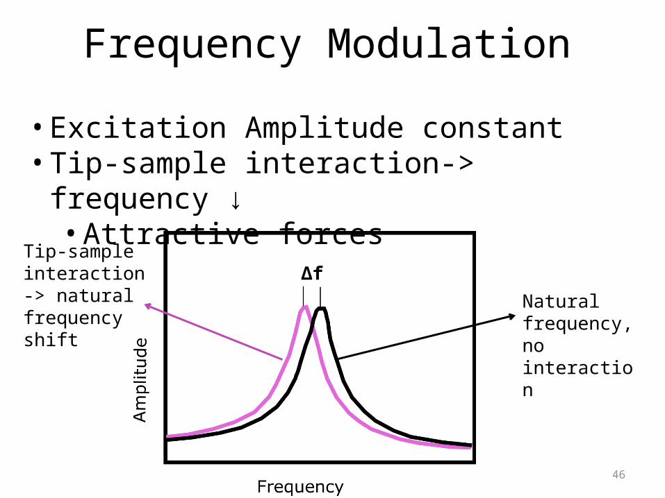
Frequency Modulation
• Excitation Amplitude constant• Tip-sample interaction-> frequency ↓
• Attractive forces
∆fNatural frequency, no interaction
Tip-sample interaction-> natural frequency shift
47
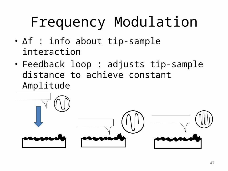
Frequency Modulation• ∆f : info about tip-sample interaction• Feedback loop : adjusts tip-sample distance to
achieve constant Amplitude

48http://www.sciencemag.org/content/337/6100/1326.figures-only
Non-contact AFM of C60A : modelB to E : AFM showing Δf at differing tip heightsF : image used for measure of bond length• measured bond
lengths are Lh = 1.38Å
• Lp = 1.454 Å
STM image

49
"C60a" by Original uploader was Mstroeck at en.wikipedia Later versions were uploaded by Bryn C at en.wikipedia. - Originally from en.wikipedia; description page is/was here.. Licensed under CC BY-SA 3.0 via Wikimedia Commons - http://commons.wikimedia.org/wiki/File:C60a.png#/media/File:C60a.png
“p”
“h”
50
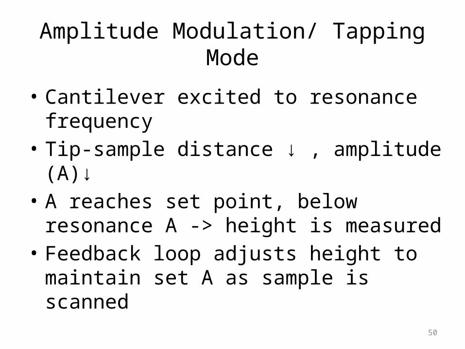
Amplitude Modulation/ Tapping Mode
• Cantilever excited to resonance frequency• Tip-sample distance ↓ , amplitude (A)↓• A reaches set point, below resonance A ->
height is measured• Feedback loop adjusts height to maintain set A
as sample is scanned

51
Set-point
52
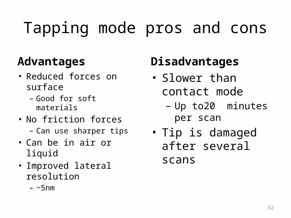
Tapping mode pros and cons
Advantages• Reduced forces on
surface – Good for soft materials
• No friction forces– Can use sharper tips
• Can be in air or liquid• Improved lateral
resolution– ~5nm
Disadvantages• Slower than contact
mode– Up to20 minutes per
scan
• Tip is damaged after several scans
53
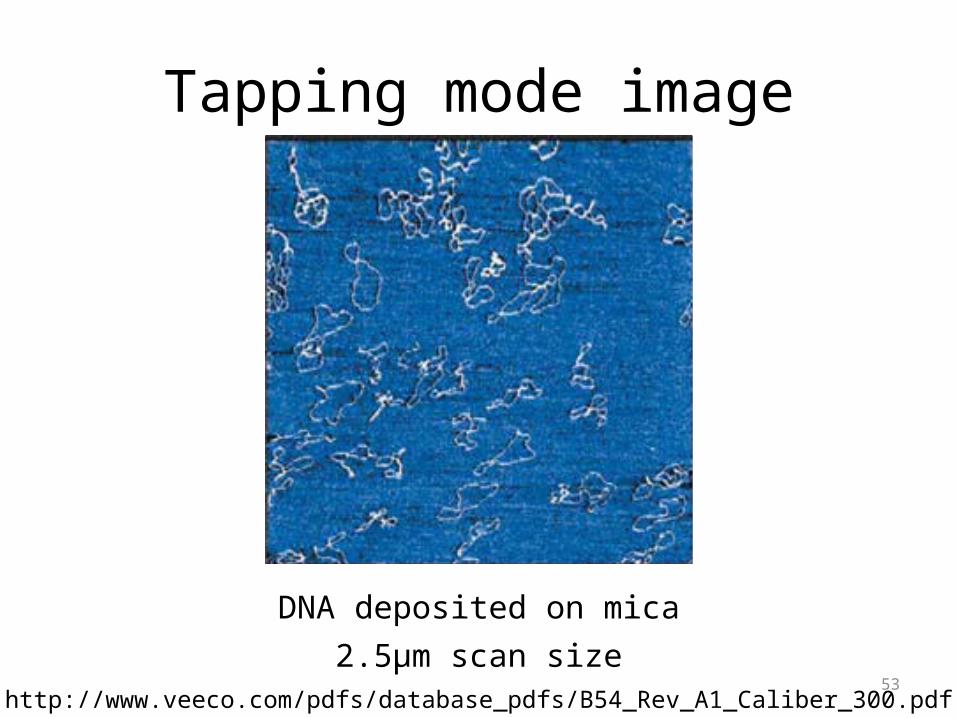
Tapping mode image
http://www.veeco.com/pdfs/database_pdfs/B54_Rev_A1_Caliber_300.pdf
2.5μm scan sizeDNA deposited on mica

54
High Resolution Image of muscovite mica in water
http://www.beilstein-journals.org/bjnano/single/articleFullText.htm?publicId=2190-4286-4-15
9.7ÅBlue : OxygenGreen : SiliconUnit Cell: 5.199Å
High-resolution dynamic atomic force microscopy in liquids with different feedback architecturesJohn Melcher, David Martínez-Martín, Miriam Jaafar, Julio Gómez-Herrero, Arvind Raman
Beilstein J. Nanotechnol. 2013, 4, 153–163.
55
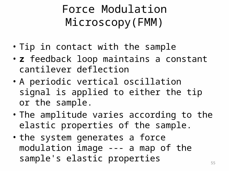
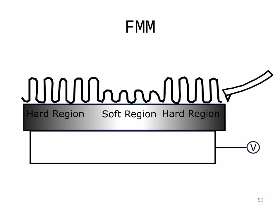
Force Modulation Microscopy(FMM)
• Tip in contact with the sample• z feedback loop maintains a constant
cantilever deflection• A periodic vertical oscillation signal is applied
to either the tip or the sample. • The amplitude varies according to the elastic
properties of the sample. • the system generates a force modulation
image --- a map of the sample's elastic properties
56
FMM

57
FMM vs AFM
Carbon fiber/polymer Composite Collected Simultaneously (5μm)
FMM gives more detailed information about the composition and distribution of the two components --- soft polymer (dark area) and hard carbon fiber.
FMM AFM

58
2-phase block copolymer
AFM FMM
The softer, more compliant component of the polymer maps in black. 900nm scans. Veeco.

59
Magnetic Force Microscopy (MFM)
• Tip is coated with a ferromagnetic film(Ni, Fe, Co)
• Scanned in non contact mode• Provides high resolution image of magnetic
patterns• Strength of local magnetic interaction
determines the vertical motion of the tip• Detectable magnetic field ~0.1 gauss (10
microteslas)

60
Magnetic Force• Described as:
: magnetic permeability of free space (4π 10-7
WbA-1m-1)
: magnetic moment of the tip:strength of magnetic field from sample
61
MFM Limitations
• Type of tip and magnetic coating affect image• Interaction of magnetic field of tip and sample
can alter each others field• Highly dependent on scan height• Inner and surface magnetic charges not able
to be deconstructed
62
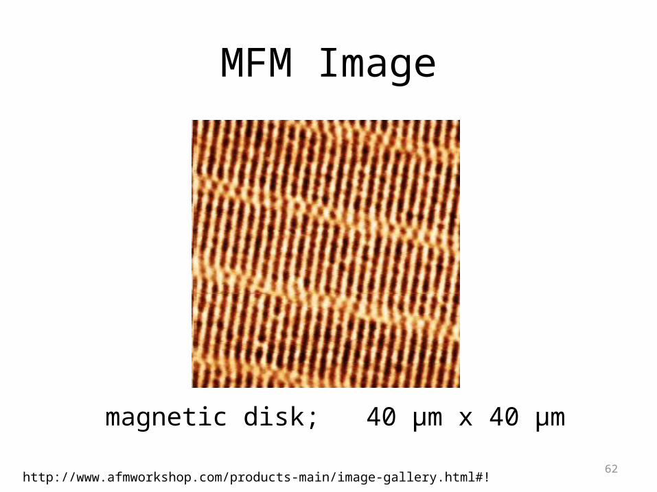
MFM Image
magnetic disk; 40 µm x 40 µm
http://www.afmworkshop.com/products-main/image-gallery.html#!

63
MFM Image
http://commons.wikimedia.org/wiki/File:MFM_AFM_JANUSZ_REBIS_INFOCENTRE_PL_HDD_MAGNETIC_MEMORY_EVOLUTION.png#/media/File:MFM_AFM_JANUSZ_REBIS_INFOCENTRE_PL_HDD_MAGNETIC_MEMORY_EVOLUTION.png
3.2GB hard drive 30GB hard drive
64
Electric Force Microscopy(EFM)
• Measures electric field gradient distribution on sample surface
• Tip : electrically conducting coating • applied Voltage between tip and sample• Deflection of cantilever charge density of
sample• Use photo-diode detector

65
EFM
66
Applications of EFM
• characterizing surface electrical properties• Interfacial charge transport and separation for
organic/electrode devices (conducting polymer, organic semiconductors, etc.)
• detecting defects of an integrated circuit (silicon surface)
• measuring the distribution of a particular material on a composite surface.
67
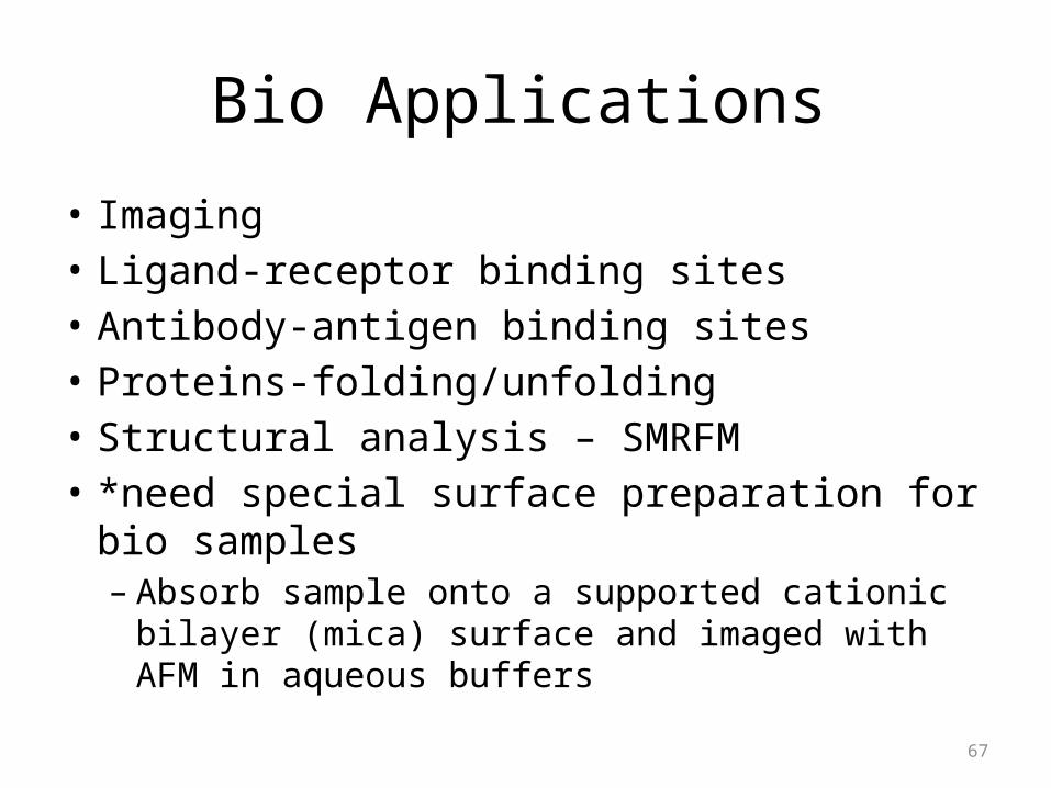
Bio Applications
• Imaging• Ligand-receptor binding sites• Antibody-antigen binding sites• Proteins-folding/unfolding• Structural analysis – SMRFM• *need special surface preparation for bio samples
– Absorb sample onto a supported cationic bilayer (mica) surface and imaged with AFM in aqueous buffers

68
DNA on multiple mica layers
2 μm X 2 μm
http://www.afmworkshop.com/products-main/image-gallery.html#!AFM_scan_DNA_mica_pm

69
Red Blood Cells, 30μm X 30μm
http://www.afmworkshop.com/products-main/image-gallery.html#!07_img_blood_cells_01_big
70
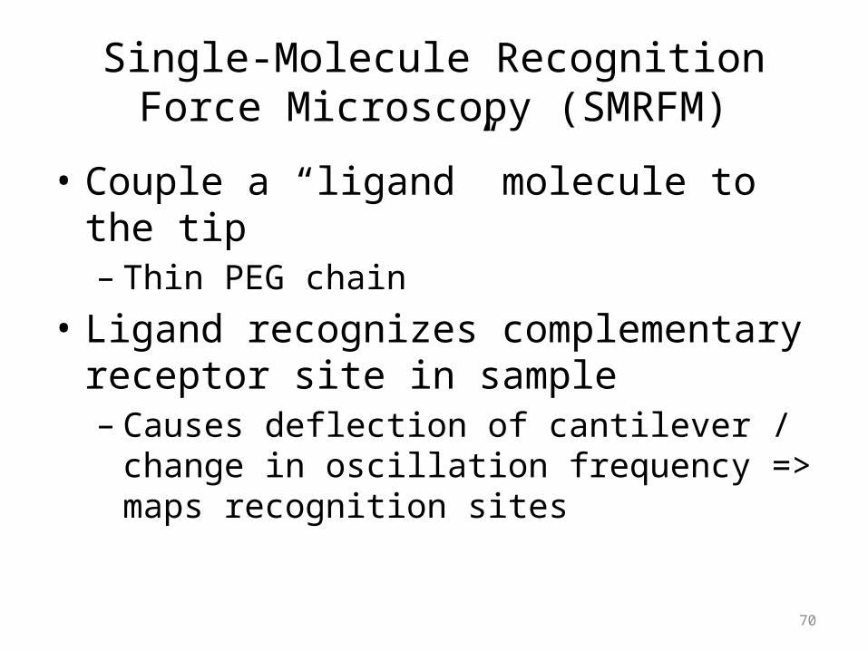
Single-Molecule Recognition Force Microscopy (SMRFM)
• Couple a “ligand” molecule to the tip– Thin PEG chain
• Ligand recognizes complementary receptor site in sample– Causes deflection of cantilever / change in
oscillation frequency => maps recognition sites

71
SMRFM
http://www.jku.at/biophysics/content/e54633/e54706/e54710/#fig1
1. NH2 on tip reacts with NHS ester of PEG linker2. Protein attached to free end of PEG (amine-aldehyde linkage)

72
How cell membranes respond to their environment
http://www.innovations-report.com/html/reports/life-sciences/report-47236.html
Simon Scheuring , Thomas Boudier , James N. Sturgis
AFM Image
Light harvesting Complex
Reaction centers
• Membrane organization in photosynthetic bacteria
• –Rsp. Photometricum• (exposed to strong
light)

73
Questions
• THANK YOU!!


