Electrostatic Discharge Control The purpose of this practice is to provide an overview of ESD phenomena and how ESD can be controlled in order to improve the performance of our network and to lower operating costs.
Audience: All network employees
Effective Date10/15/2009
Issue Date: Issue 2, 10/01/2009
Expires On: NA
Related Documents: None
Cancelled Documents: None
Issuing Department: Global Engineering Support – Common Systems
Business Unit: AT&T Services, Inc.
Author(s): John Messina, Telephone 203-553-0232, ATTUID JM4735
INTRODUCTION This practice provides an overview of ESD phenomena. Network operating performance and service reliability is maximized and operating costs are reduced through diligent and effective ESD control and operating procedures.
REASON FOR REISSUE Issue Date Description of Changes Author
Issue Date Description of Changes Author 1 02/01/2004 Convert BSP 010-700-901MP to SBC-TP-
4.3 Triboelectric Series .............................................................................................................................. 6
4.4 Material Characteristics ...................................................................................................................... 6
1.0 PURPOSE Electrostatic discharge (ESD) is considered one of the major causes of defective circuit packs in our network. ESD affects virtually every solid state component in our network, including transistors, integrated circuits and MOS (metal-oxide-silicon) devices. In most cases, the damaging discharge can neither be seen nor felt. The purpose of this practice is to provide an overview of ESD phenomena and how ESD can be controlled in order to improve the performance of our network and to lower operating costs.
This practice applies to all AT&T regions and is intended for all engineering, operations and contract personnel as well as personnel in procurement (i.e. shipping and receiving) who may handle circuit packs as part of their day-to-day responsibilities.
2.0 SCOPE The contents of this practice apply to all employees and contract personnel who come in contact with ESD-sensitive equipment used in any network element (switching, transport, loop, power, etc.) in all locations, including but not limited to central offices, controlled environmental vaults, cabinets and huts (electronic equipment enclosures). The contents also apply to AT&T equipment located at customer locations.
All equipment containing solid state electronic components is considered ESD-sensitive.
In this practice the term circuit pack is equivalent to terms such as plugs, plug-ins, plug-in units (PIUs), printed wiring boards (PWBs), circuit boards, packs, cards, etc. Whenever information contained in this document conflicts with a standard published by an authority having jurisdiction over safety-related practices and procedures (e.g., NEC or OSHA), those published standards shall take precedence over the applicable text of this document.
3.0 DEFINITIONS Antistatic - A property of materials that resist triboelectric charging and produce minimal static charge when separated from themselves or other materials. A material's antistatic property is not necessarily correlated with its resistivity.
Antistatic Solution - A solution that provides a static dissipative coating to material.
Charge - An excess or deficiency of electrons on the surface of a material, measured in coulombs.
Circuit Pack - An assembled printed circuit board with components (resistors, diodes, transistors, integrated circuits, etc.).
Common Point Ground – A system of connecting two or more grounding connectors to the same electrical potential.
Conductive - Material exhibiting a surface resistivity of <105 ohms per square or a volume resistivity of <104 ohm-cm.
Dissipative - Material exhibiting a surface resistivity of between 105 and 1012 ohms per square or a volume resistivity of between 104 through 1011 ohms-cm.
Electromagnetic Interference (EMI) - An electromagnetic disturbance that degrades the performance of electronic equipment.
Electrostatic Charge - An electric charge at rest.
Electrostatic Discharge (ESD) - The rapid, spontaneous transfer of electrostatic charge induced by a high electrostatic field.
Electrostatic Field - An attractive or repulsive force in space due to the presence of an electric charge.
Electrostatic Shield - A barrier or enclosure that limits the penetration of an electrostatic field.
ESD Sensitive – A device or circuit pack that is sensitive to ESD damage.
Field Induction – The process by which a charge's field establishes a charge in a nearby conductive object without physical contact.
Ground - A conducting connection, whether intentional or accidental, between an electrical circuit or equipment and the earth, or to some conducting body that serves in place of the earth.
Insulative - Material having a surface resistivity >1012 ohms per square or a volume resistivity
>1011 ohm-cm.
lonization - The process by which neutral atoms or molecules acquire a positive or negative charge.
Ionizer - A device designed to generate positive and/or negative air ions.
NO-OX-ID "A" – A general term applied to any one of a number of coatings manufactured by Sanchem (or others) that protect against corrosion and the formation of rust. NO-OX-ID "A" is conductive and made especially for electrical applications.
Surface Resistivity - The ratio of DC voltage drop per unit length to the surface current per unit width. It is independent of the size of the square or its dimensional units and is expressed in ohms/square.
Triboelectric Charging – The generation of electrostatic charges when two materials make contact or are rubbed together and then separated.
Volume Resistivity - The ratio of DC voltage drop per unit thickness to the amount of current per unit area passing through the material. It is independent of the volume of the material and is expressed in ohm-length (usually ohm-meter or ohm-centimeter).
Network acronyms can be found in SBC-000-000-020, Network Acronyms Dictionary.
4.0 ESD FUNDAMENTALS 4.1 Static Electricity Static electricity is defined as an electrical charge caused by an imbalance of electrons on the surface of a material. This imbalance of electrons produces an electric field that is strong enough to be measured and that can have a disruptive influence on nearby objects. This electrical charge may be transferred from one material to another by way of an electrostatic discharge.
Electrostatic discharges can destroy a semiconductor device, degrade the electrical characteristics of a semiconductor device, alter normal operation of an electronic system and/or corrupt data transmission. Studies completed in the 1990s concluded that, within the telecommunications industry, an average of 30% of all circuit pack failures were due to electrostatic discharge events.
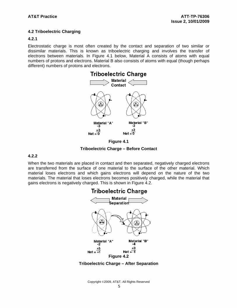
4.2 Triboelectric Charging 4.2.1 Electrostatic charge is most often created by the contact and separation of two similar or dissimilar materials. This is known as triboelectric charging and involves the transfer of electrons between materials. In Figure 4.1 below, Material A consists of atoms with equal numbers of protons and electrons. Material B also consists of atoms with equal (though perhaps different) numbers of protons and electrons.
Figure 4.1
Triboelectric Charge – Before Contact 4.2.2 When the two materials are placed in contact and then separated, negatively charged electrons are transferred from the surface of one material to the surface of the other material. Which material loses electrons and which gains electrons will depend on the nature of the two materials. The material that loses electrons becomes positively charged, while the material that gains electrons is negatively charged. This is shown in Figure 4.2.
4.3 Triboelectric Series 4.3.1 The amount of charge created by the contact and separation of two materials is largely dependent on the type of materials, area of contact, speed of separation and humidity. An electrostatic charge may also be created on a material in other ways such as by induction, ion bombardment or contact with another charged object. However, within the telecommunications environment, triboelectric charging is by far the most prevalent means of electrostatic charging.
4.3.2 The relative amount of triboelectric charging on two materials (that have made contact and then are separated) can be determined from Table 4.1. The triboelectric Series is a loose ranking of a material’s polarity when triboelectrically charged with another material. The materials at the top of the series will typically have a more positive charge than a material lower in the series and the more separation in the series, the higher the resultant charge will be.
MATERIAL RELATIVE CHARGE Air MOST POSITIVE Human Hands Asbestos Rabbit Fur Acetate Glass Nylon Wool Lead Silk Aluminum Paper Cotton Neutral Steel Mylar Copper Gold Polyester Acrylic PVC (Vinyl) Teflon Most Negative
Table 4.1
Triboelectric Series 4.4 Material Characteristics Virtually all materials, including water and dirt particles in the air, can be triboelectrically charged. How much charge is generated, how quickly it is charged and how the charge is distributed on the material are functions of the materials' electrical characteristics. For static control purposes, materials are categorized as insulative, dissipative or conductive.
4.4.1 Insulative Material An insulative material (or insulator) prevents or limits the flow of electrons across its surface or through its volume. Insulators have an extremely high electrical resistance although a considerable amount of charge can be generated on the surface of an insulator. Because an insulative material does not readily allow the flow of electrons, both positive and negative charges can reside on an insulative surface at the same time, although at different locations. Electrons cannot easily flow across the insulative material's surface and charges may remain in place for a very long time.
4.4.2 Conductive Material A conductive material (or conductor), because it has low electrical resistance, allows electrons to flow easily across its surface or through its volume. When a conductive material becomes charged, the charge (i.e., the deficiency or excess of electrons) will be uniformly distributed across the surface of the material. If a charged conductive material makes contact with a second conductive material, the electrons will transfer between the materials quite easily. If the second conductor is attached to an earth ground point, the electrons will flow to ground and the excess charge on the conductor will be "neutralized." Wrist straps rely on this principle.
4.4.3 Dissipative Materials Static dissipative materials have electrical resistance between that of insulative and conductive materials. There can be electron flow across or through the dissipative material, but it is controlled by the surface resistance or volume resistance of the material. As with the other two types of materials, charge can be generated triboelectrically on a static dissipative material. However, like the conductive material, the static dissipative material will allow the transfer of charge to ground or to other conductive objects. The transfer of charge from a static dissipative material will generally take longer than from a conductive material of equivalent size. Charge transfers from static dissipative materials are significantly faster than from insulators, and slower than from conductors.
4.5 Failure Modes ESD damage is usually caused by one of three events: direct electrostatic discharge to the device, electrostatic discharge from the device or field-induced discharges. These failures can be catastrophic (immediate and permanent damage to the device or circuit pack) or latent (the device or circuit pack will continue to perform but with decreased operating life). NOTE: It is important to understand that damaging discharges occur even though there may be no audible or visual effects.
4.5.1 Discharge to the Device An ESD event can occur when any charged conductor (including the human body) discharges to an electrostatic discharge sensitive device (ESDS). The most common cause of electrostatic damage is the direct transfer of electrostatic charge from the human body or a charged material to the (ESDS) device. When a person walks across a floor, an electrostatic charge accumulates on the body. Simple contact of a finger to the leads of an ESDS device or assembly allows the body to discharge, possibly causing device damage. A similar discharge can occur from a charged conductive object, such as a metallic tool or fixture.
4.5.2 Discharge from the Device The transfer of charge from an ESD sensitive device is also an ESD event. When circuit packs or individual devices are handled without proper control measures, a charge will accumulate on the circuit pack or device. If it then contacts another conductive surface, a rapid discharge
occurs from the device to the conductive object. Although the duration of the discharge is very short--often less than one nanosecond--the peak current can reach 10 amperes or more.
4.5.3 Field Induced Discharges Another event that can directly or indirectly damage devices is termed Field Induction. Whenever any object, such as the hand in Figure 4.3, becomes charged, there is an electrostatic field associated with that charge. If an ESDS device is placed in that electrostatic field, a charge may be induced on the device. If the device is then momentarily grounded while within the electrostatic field, a transfer of charge from the device occurs.
NOTE: It is possible to damage a device even though no physical contact has been made.
Figure 4.3
Electrostatic Induction 4.6 Device Sensitivity 4.6.1 Charge Dissipation Damage to an ESDS device by the ESD event is determined by the device's ability to dissipate the energy of the discharge and / or withstand the voltage levels involved. This is known as device "ESD sensitivity". Test procedures based on the models of ESD events help define the sensitivity of components to ESD. Some devices may be more readily damaged by discharges occurring within automated equipment, while others may be more prone to damage from handling by personnel.
4.6.2 Voltage Tolerance Many electronic components are susceptible to ESD damage at relatively low voltage levels. Some are susceptible to damage at less than 100 volts and most disk drive components have sensitivities below 10 volts. Current trends in product design are to pack more and more circuitry into the same small space (semiconductor traces less than 1 micron) while at the same time lowering logic levels (2 volts and less) and increasing operating rates (100Mbs and higher). The very characteristics that make these devices so attractive, small size, low operating voltages and high operating speed, are also what make them so susceptible to ESD.
Device Type Range of Sensitivity (volts) Film Resistors 300 - 3000 CMOS 200 - 3000 Operational Amplifier 190 – 2500 Transistors 140 – 7000 EPROM 100 – 2500 VMOS 30 – 1800 MOSFET 10 – 100
Table 4.2 Semiconductor Device Sensitivity
5.0 ESD CONTROL PRINCIPLES The potential for harmful electrostatic discharge exists throughout a product’s lifecycle. Beginning with the manufacturing process and continuing through the testing, shipping, receiving, installation, operation and maintenance processes, the potential for ESD damage is present.
Despite the broad exposure to ESD events for both components and systems, the control of damaging ESD events can be accomplished by focusing on just four basic principles: Immunity by Design, Reduce Charge Generation, Dissipate Charges and Protect Products. Through our policies and procedures, AT&T addresses all four principles although the majority of our day-to-day efforts are focused on dissipation of charges and protection of products.
5.1 Immunity by Design The control of ESD begins with the manufacturer’s design of solid state components and electronic systems. Manufacturers can improve the robustness of their products by selection of less static sensitive devices (see Table 4.2) and by providing protection on devices, boards, assemblies and systems. AT&T has the least influence over this ESD control measure but we do make considerable effort to evaluate products per ATT-TP-76200 for compliance with our standards for ESD immunity.
AT&T document ATT-TP-76200 provides the requirements and objectives to be met by manufacturers for equipment intended for use in our network. These requirements include testing for ESD immunity, product labeling to alert users that the equipment is ESD sensitive and product maintenance documentation that addresses ESD mitigation and dissipation.
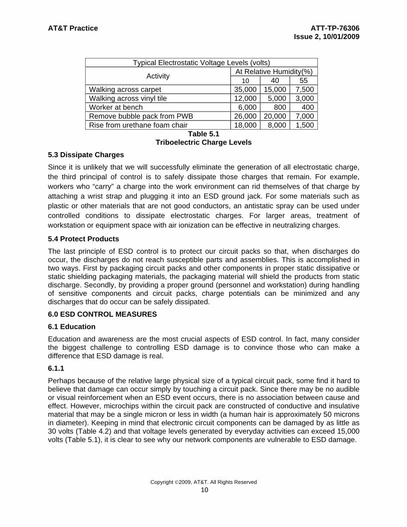
5.2 Reduce Charge Generation The second principal of control is to eliminate or reduce the generation and accumulation of electrostatic charge. The concept is basic – if there is no charge then there will be no discharge. This is done by reducing static generating processes and materials and by keeping materials at the same electrostatic potential. Minimizing contact of materials that are at the opposite ends of the Triboelectric Series in Table 4.1, selection of flooring and work surface material can all help reduce static generation. Maintaining objective levels of humidity (nominally 30%) will also serve to minimize the generation of static charges (see Table 5.1 below).
Walking across carpet 35,000 15,000 7,500 Walking across vinyl tile 12,000 5,000 3,000 Worker at bench 6,000 800 400 Remove bubble pack from PWB 26,000 20,000 7,000 Rise from urethane foam chair 18,000 8,000 1,500
Table 5.1 Triboelectric Charge Levels
5.3 Dissipate Charges Since it is unlikely that we will successfully eliminate the generation of all electrostatic charge, the third principal of control is to safely dissipate those charges that remain. For example, workers who “carry” a charge into the work environment can rid themselves of that charge by attaching a wrist strap and plugging it into an ESD ground jack. For some materials such as plastic or other materials that are not good conductors, an antistatic spray can be used under controlled conditions to dissipate electrostatic charges. For larger areas, treatment of workstation or equipment space with air ionization can be effective in neutralizing charges.
5.4 Protect Products The last principle of ESD control is to protect our circuit packs so that, when discharges do occur, the discharges do not reach susceptible parts and assemblies. This is accomplished in two ways. First by packaging circuit packs and other components in proper static dissipative or static shielding packaging materials, the packaging material will shield the products from static discharge. Secondly, by providing a proper ground (personnel and workstation) during handling of sensitive components and circuit packs, charge potentials can be minimized and any discharges that do occur can be safely dissipated.
6.0 ESD CONTROL MEASURES 6.1 Education Education and awareness are the most crucial aspects of ESD control. In fact, many consider the biggest challenge to controlling ESD damage is to convince those who can make a difference that ESD damage is real.
6.1.1 Perhaps because of the relative large physical size of a typical circuit pack, some find it hard to believe that damage can occur simply by touching a circuit pack. Since there may be no audible or visual reinforcement when an ESD event occurs, there is no association between cause and effect. However, microchips within the circuit pack are constructed of conductive and insulative material that may be a single micron or less in width (a human hair is approximately 50 microns in diameter). Keeping in mind that electronic circuit components can be damaged by as little as 30 volts (Table 4.2) and that voltage levels generated by everyday activities can exceed 15,000 volts (Table 5.1), it is clear to see why our network components are vulnerable to ESD damage.
6.1.2 As integrated circuit packages continue to get more and more dense (>1,000,000 transistors on a single chip), we can expect that semiconductor devices and circuit packs will become even more susceptibility to ESD damage. Fortunately, with a modest investment in ESD control measures, ESD losses can be minimized with a resultant improvement in network reliability and reduced operating cost.
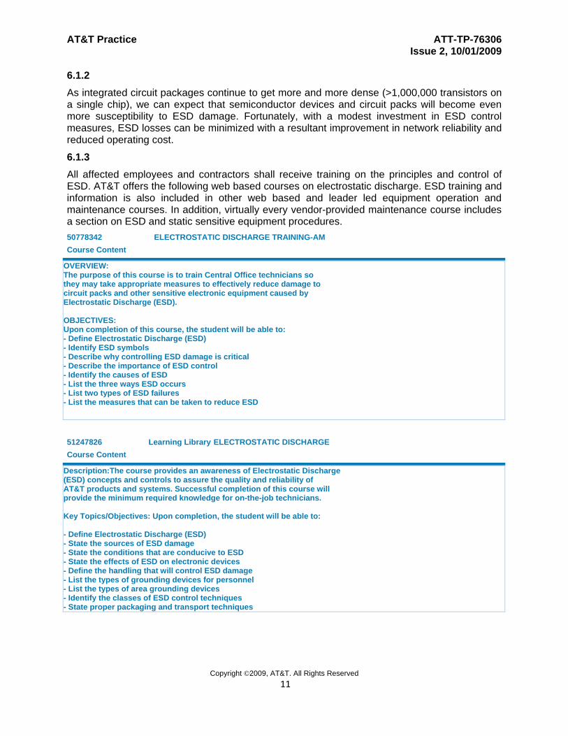
6.1.3 All affected employees and contractors shall receive training on the principles and control of ESD. AT&T offers the following web based courses on electrostatic discharge. ESD training and information is also included in other web based and leader led equipment operation and maintenance courses. In addition, virtually every vendor-provided maintenance course includes a section on ESD and static sensitive equipment procedures. 50778342 ELECTROSTATIC DISCHARGE TRAINING-AMCourse Content
OVERVIEW: The purpose of this course is to train Central Office technicians so they may take appropriate measures to effectively reduce damage to circuit packs and other sensitive electronic equipment caused by Electrostatic Discharge (ESD). OBJECTIVES: Upon completion of this course, the student will be able to: - Define Electrostatic Discharge (ESD) - Identify ESD symbols - Describe why controlling ESD damage is critical - Describe the importance of ESD control - Identify the causes of ESD - List the three ways ESD occurs - List two types of ESD failures - List the measures that can be taken to reduce ESD 51247826 Learning Library ELECTROSTATIC DISCHARGECourse Content
Description:The course provides an awareness of Electrostatic Discharge(ESD) concepts and controls to assure the quality and reliability of AT&T products and systems. Successful completion of this course will provide the minimum required knowledge for on-the-job technicians. Key Topics/Objectives: Upon completion, the student will be able to: - Define Electrostatic Discharge (ESD) - State the sources of ESD damage - State the conditions that are conducive to ESD - State the effects of ESD on electronic devices - Define the handling that will control ESD damage - List the types of grounding devices for personnel - List the types of area grounding devices - Identify the classes of ESD control techniques - State proper packaging and transport techniques
6. 2 Tools and Material Various tools and material are available to implement an effective ESD control program including:
• Wrist Straps • Common Point Ground • Test Equipment • Labels, Signs and Posters • Fixed Workstation • Packaging • Portable Workstation • Storage
6.2.1 Wrist Straps A wrist strap is considered the “first line of defense” against the effects of electrostatic discharge and is the most cost-effective ESD counter-measure available. Always moving and moving things around us, people cause more ESD-related damage and problems than any other source.
When used appropriately, the wrist strap can keep personnel voltages low thereby avoiding one of the most potent sources of ESD accumulation in the work environment - a charged human body. The purpose of a wrist strap is to safely drain body charges and to safely keep the body at or near ground potential.
6.2.1.1 Employees handling unprotected circuit packs should be issued their own approved wrist strap and it shall be worn at all times and connected to a known ground point when handling a circuit pack that is being placed or removed from service or is otherwise not in its protective container. Wrist straps shall also be worn during any installation or maintenance activity when contact with equipment is required (e.g., plugging in a Craft Interface Device, adjusting panel controls, or making backplane connections).
6.2.1.2 To maintain continuity between the wearer's skin and the wrist strap ground point, the band of the wrist trap should be properly adjusted to maintain continuity with the wearer's skin.
6.2.1.3 Spare wrist straps should be available to provide a quick replacement for wrist straps that fail the daily test routine (see section 5.2.2)
6.2.1.4 Approved ESD heel straps and footwear may be used in areas where the use of wrist straps is deemed impracticable.
6.2.1.5 An alligator clip may be attached to the plug of a wrist strap for use in locations where a ground jack is not readily available and where a known ground point is available.
6.2.2 Test Equipment 6.2.2.1 Wrist Strap Tester All wristband and heel strap assemblies shall be tested each day the devices are used and shall be replaced when found defective. A “Go/No-Go” type wrist strap or heel strap tester using LEDs and an audible tone should be used to test the integrity of the wristband and cord system. The tester should be available at a location that facilitates daily testing of wrist straps. For more
information on wrist strap testers, refer to Telcordia’s GR-1418-CORE Generic Requirements for Wrist Strap Testers. When a wrist strap assembly is tested, the band shall first be properly adjusted to the wrist. Then the cord should be moved from side to side and subjected to a slight pulling stress to expose intermittent failures.
NOTE: In the absence of a wrist strap tester, the wrist strap assembly can be tested with a volt-ohm meter (VOM). The reading should be between 0.75 and 1.2 megohms.
6.2.2.2 Electrostatic Field Meter Electrostatic field meters are used regularly to conduct audits in order to determine representative charge levels within the work environment. One of the more important uses of an electrostatic field meter may be as an educational tool to demonstrate to new employees what levels of static charge exist on their body and within the workplace.
6.2.2.3 Ionization Tester Ionization testers are most often used in and around fixed workstations that have ionization systems. The testers verify that charges are being emitted and they check for balance between positive and negative ions.
6.2.3 Fixed Workstation Components of a fixed workstation may include a grounded workbench, a chair with conductive casters, a grounded work surface (mat) made of dissipative material, a grounded floor mat made of dissipative material, wrist straps, heel straps, common point ground, air ionizer, static dissipative containers and static shield containers. A fixed, antistatic workstation (Figure 6.1) makes it easier to perform repetitive operations like setting circuit pack options on a large number of circuit packs or preparing a large number of circuit packs for shipment.
Figure 6.1
Fixed Workstation 6.2.4 Portable Work Station A portable antistatic workstation (field service kit) is required for maintenance and repair at all equipment locations including the central office, a controlled environmental vault, a field cabinet
or hut. The minimum requirements for a portable workstation include a wrist strap, a grounded dissipative mat and a common ground point. The use of a static dissipative mat provides a discharge path for all conductive objects placed on it (such as circuit packs, tote boxes, bags, tools, etc.).
6.2.5 Common Point Ground All locations where unprotected circuit packs may be handled shall be equipped with a means to ground wrist straps or similar devices that require a connection to ground. This includes all network equipment locations, fixed or portable workstations, storage cabinets and all shipping and receiving points.
The preferred wrist strap connection point is an ESD ground jack. An ESD ground jack, incorporated on a network element equipment shelf, grounded per ATT-TP-76416 and installed per ATT-TP-76300, shall be considered an approved ESD Ground Point. If a new or existing equipment rack, frame or cabinet equipped with or intended to be equipped with electronic equipment has no ESD grounding jack(s) on the installed shelves, one shall be installed on the right framework upright. In the absence of a ground jack, an alligator clip adaptor or similar device that connects to the banana plug of the wrist strap cord may be used for connection to a known ground point on the equipment bay. Most unpainted screws, nuts, bolts or equipment mounting plates will serve as an effective ground point.
Note: An ESD ground jack is not required on any equipment, rack, frame or cabinet, such as a fiber distribution bay, that does not have or will not have any electronic equipment or circuit packs either powered or stored.
6.2.5.2 Frame mounted ESD jacks shall be assembled per Figure 6.2. It is preferred that the area surrounding the hole for the jack be masked to provide an unpainted surface for the jack that is visible after installation. An external tooth lockwasher, flat washer and nut shall be installed in that sequence to the back side of the assembly. The flat washer is required in all applications to insure that the teeth of the external tooth lockwasher properly engage with the framework since the nuts provided with the jack assemblies do not have sufficient diameter to apply pressure to the lockwasher teeth. See ATT-E-00174-E on the Woodduck site for additional information.
Standard4mm ESD Jack
Frame
Nut
Lock Washer
Flat Washer
Figure 6.2
Ground Jack Assembly Previously installed ESD jacks utilizing an uninsulated a# 8 AWG ring type crimp connector shall be grandfathered.
6.2.5.3 A common ground point shall be used for all grounding conductors (wrist straps, work mats, floor mats, etc.) at an antistatic workstation.
6.2.6 Labels, Signs and Posters 6.2.6.1 All frame and cabinet wrist strap ground points shall be labeled. The label should read “ESD Common Point Ground” or otherwise identify the connection as the ESD ground point. Figure 6.3 is the industry approved Ground Point label.
Figure 6.3
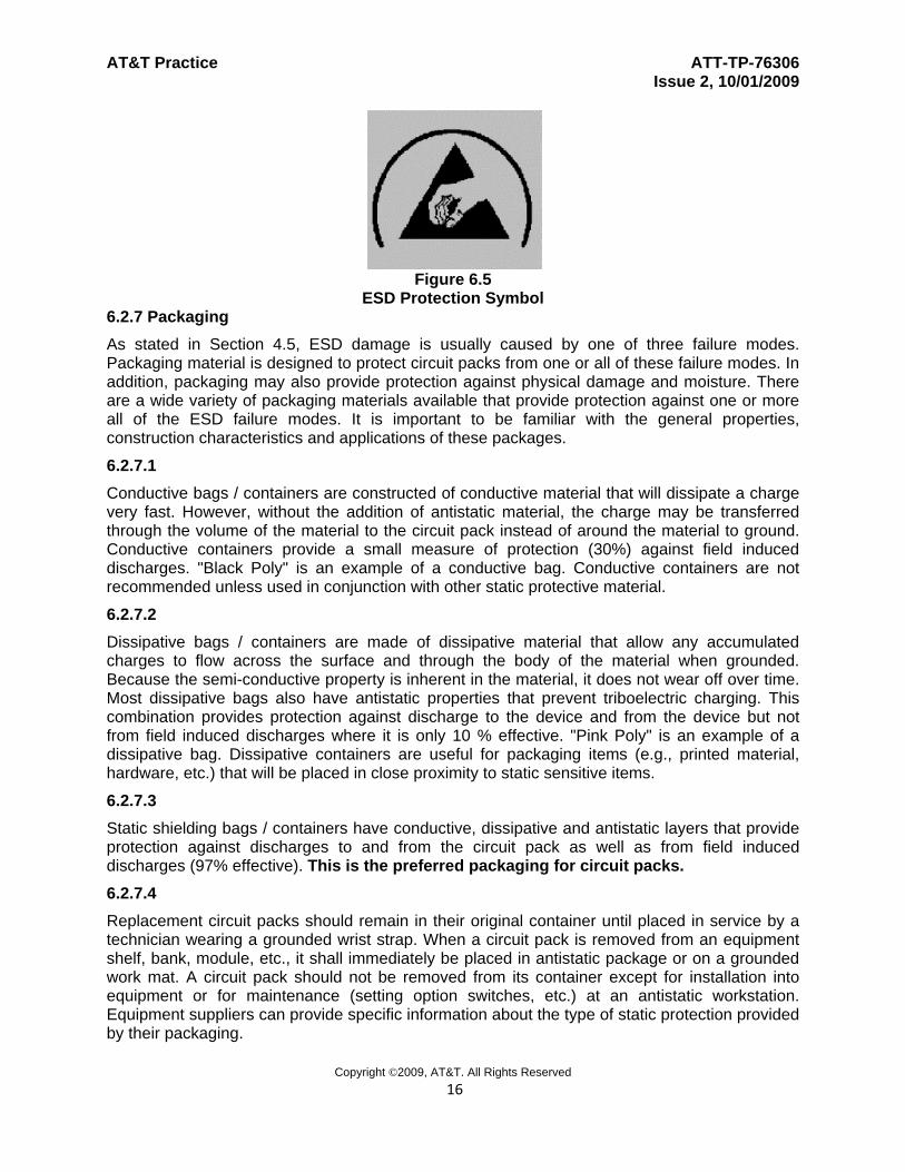
ESD Wrist Strap Ground Point 6.2.6.2 Figure 6.4 shows the universal ESD susceptibility symbol indicating the presence of static sensitive devices, assemblies or systems. This symbol appears on labels and signs to alert personnel of the need for special handling of equipment. Figure 6.5 shows the universal symbol indicating protection to ESD sensitive devices. This symbol can be used to identify tools, material and equipment that are specifically designed to provide ESD protection.
6.2.6.3 The use of ESD signs, labels and posters is encouraged to promote ESD awareness. These are available through a number of companies that specialize in ESD-related products.
ESD Protection Symbol 6.2.7 Packaging As stated in Section 4.5, ESD damage is usually caused by one of three failure modes. Packaging material is designed to protect circuit packs from one or all of these failure modes. In addition, packaging may also provide protection against physical damage and moisture. There are a wide variety of packaging materials available that provide protection against one or more all of the ESD failure modes. It is important to be familiar with the general properties, construction characteristics and applications of these packages.
6.2.7.1 Conductive bags / containers are constructed of conductive material that will dissipate a charge very fast. However, without the addition of antistatic material, the charge may be transferred through the volume of the material to the circuit pack instead of around the material to ground. Conductive containers provide a small measure of protection (30%) against field induced discharges. "Black Poly" is an example of a conductive bag. Conductive containers are not recommended unless used in conjunction with other static protective material.
6.2.7.2 Dissipative bags / containers are made of dissipative material that allow any accumulated charges to flow across the surface and through the body of the material when grounded. Because the semi-conductive property is inherent in the material, it does not wear off over time. Most dissipative bags also have antistatic properties that prevent triboelectric charging. This combination provides protection against discharge to the device and from the device but not from field induced discharges where it is only 10 % effective. "Pink Poly" is an example of a dissipative bag. Dissipative containers are useful for packaging items (e.g., printed material, hardware, etc.) that will be placed in close proximity to static sensitive items.
6.2.7.3 Static shielding bags / containers have conductive, dissipative and antistatic layers that provide protection against discharges to and from the circuit pack as well as from field induced discharges (97% effective). This is the preferred packaging for circuit packs. 6.2.7.4 Replacement circuit packs should remain in their original container until placed in service by a technician wearing a grounded wrist strap. When a circuit pack is removed from an equipment shelf, bank, module, etc., it shall immediately be placed in antistatic package or on a grounded work mat. A circuit pack should not be removed from its container except for installation into equipment or for maintenance (setting option switches, etc.) at an antistatic workstation. Equipment suppliers can provide specific information about the type of static protection provided by their packaging.
6.2.7.5 The effectiveness of antistatic and static shielding bags / containers will diminish over time. Check with individual manufacturers for the expected useful life.
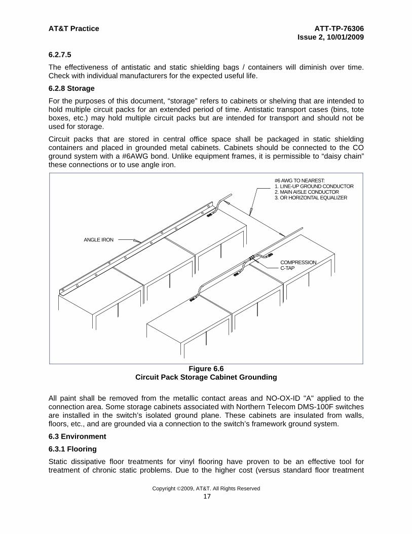
6.2.8 Storage For the purposes of this document, “storage” refers to cabinets or shelving that are intended to hold multiple circuit packs for an extended period of time. Antistatic transport cases (bins, tote boxes, etc.) may hold multiple circuit packs but are intended for transport and should not be used for storage.
Circuit packs that are stored in central office space shall be packaged in static shielding containers and placed in grounded metal cabinets. Cabinets should be connected to the CO ground system with a #6AWG bond. Unlike equipment frames, it is permissible to “daisy chain” these connections or to use angle iron.
#6 AWG TO NEAR1. LINE-UP2. MAIN AISLE C3. OR HORIZONT
EST: GROUND CONDUCTOR
ONDUCTORAL EQUALIZER
COMPRESSIOC-TAP
N
ANGLE IRON
Figure 6.6 Circuit Pack Storage Cabinet Grounding
All paint shall be removed from the metallic contact areas and NO-OX-ID "A" applied to the connection area. Some storage cabinets associated with Northern Telecom DMS-100F switches are installed in the switch’s isolated ground plane. These cabinets are insulated from walls, floors, etc., and are grounded via a connection to the switch’s framework ground system.
6.3 Environment 6.3.1 Flooring Static dissipative floor treatments for vinyl flooring have proven to be an effective tool for treatment of chronic static problems. Due to the higher cost (versus standard floor treatment
products) and the temporary nature of the solution, floor treatments should only be considered in extreme circumstances.
Antistatic carpet does provide a level of ESD control and is recommended in areas such as operator position locations. However, carpets tend to contain dirt and other particulates that can harm electronic equipment. For this reason, carpeting is not suitable for a central office environment.
6.3.2 Humidity In a humid environment, moisture absorbed on the surface of an object will provide a leakage path to ground resulting in a low static potential. In dry conditions, such as a heated building in wintertime or in a naturally arid climate, the leakage rate no longer equals the rate of static generation and large static potentials can result. Table 5.1 shows the effect of relative humidity on static generation. Higher humidity has less effect on materials like Teflon that do not absorb moisture. Central offices are generally kept at between 5% and 55% relative humidity.
3. Space is considered occupied when personnel report to the location on a daily basis during the work week for a minimum 8 hours per day.
Temperature Temperature Humidity
Technologies: Occupied Unoccupied3
Transport Area 60 – 78oF 55 - 85oF 15 - 55% Switch Area – General 60 – 78oF4
60 - 78oF 20 - 55% Switch Area – 1A, 4E, & Exceptions per 2.1.4
4. In SE region, unoccupied switch areas currently operated at Extended Wide Band temperature range (55 – 85oF) shall continue to be operated at this range until further notice.
Table 6.1
Operating Temperature & Humidity Levels for COs, Huts & CEVs
6.3.3 Air Filtration Central office environments should incorporate air filtration with an ASHRAE dust spot rating of 65% or better. The minimum ventilation rate is 0.25 air changes per hour or 15 cfm per person, which ever is greater. Air filtration, can help maintain humidity levels as well as minimize triboelectric charging due to particles in the air.
6.3.4 Air Ionization Ionizers neutralize a charge on the surface of a material by blowing air filled with equal numbers of negative and positive ions across the material. Materials (usually insulative materials) that must stay within the area of a fixed workstation and that are neither conductive nor readily connected to ground should be treated with air ionization. Air ionizers are generally intended to treat a single small area (such as a workstation).
NOTE: Some air ionizers produce ozone as a by-product. If so, ozone production must be within the OSHA allowance, < 0.1 parts per million.
6.3.5 Antistatic solution An antistatic solution or spray can be used to prevent static charge generation on materials that are not antistatic. While sprays or wipes may help mitigate a static problem, they do not have sufficient conductivity to act as a ground for personnel or other items. These sprays and wipes are unsuitable substitutes for wrist or heel straps in any area where static control measures are required. Antistatic solutions should be applied according to the manufacturer guidelines and must never be applied to energized parts or assemblies.
6.4 Shipping and Receiving ESD control procedures begin when we take possession of circuit packs or other ESD sensitive products and do not end until ownership passes to another party. This usually means that the first and last group to have an impact on the effectiveness of our ESD control procedures is our warehouse personnel.
All the procedures outlined in this practice also apply to warehouse personnel with the exception that circuit packs packaged in static shielding containers may be stored on open, ungrounded shelves instead of in closed and grounded storage cabinets.
7.0 SUMMARY / POLICY For convenience, key requirements for effective ESD control are repeated below:
• A properly grounded wrist strap shall be worn whenever a circuit pack is being handled outside its protective container. This also applies to handling circuit packs that are presumed to be defective.
• Circuit packs should be handled by the edges only. Avoid touching components or conductors.
• Spare wrist straps should be kept on hand for ready replacement of defective wrist straps
• Wrist straps shall be tested every day they are used. • Circuit packs should be stored in their original containers and kept in a grounded metal
cabinet or vendor-designated storage area. • Circuit packs shall be transported in a static dissipative or static shielded container. • All employees and contractors who handle circuit packs shall receive training in ESD
control • Appropriate ESD control tools and materials will be made available at all required work
locations. • Static generating material should not be allowed in areas where circuit packs are
handled. • Employees shall be informed of ESD phenomenon and understand what constitutes a
static hazard in the work place. • Employees and contractors who work with circuit packs shall be given ESD control
training. • Employees and contractors who handle, transport, store, or test circuit packs shall
observe recognized ESD precautions. • ESD awareness shall be maintained in all equipment areas. • To the maximum degree practical, static-generating material shall not be allowed in
8.0 REFERENCES The documents listed below contain material relevant to ESD control in a telecommunications environment. Many of the Telecordia documents are available on the APEX web site: http://apex.sbc.com/
ANSI/EOS/ESD S 11.11 EOS/ESD Association Standard for the Protection of Electrostatic Discharge Susceptible Items - Surface Resistance Measurement of Static Dissipative Planar Materials
ANSI/EIA 541-88, Packaging Material Standards for ESD Sensitive Items
ANSI/ESD-S20.20-1999, Development of an Electrostatic Discharge Control Program
ANSI T1.308 - 1996, American National Standard on Central Office Equipment - Electrostatic Discharge Requirements, American National Standards Institute.
ANSI T1.321-1995 (R2000), Electrical Protection for Network Operator - Type Equipment Positions
BR 010-170-005, Electrostatic Discharge, Issue 3, June 1996, Telcordia
BR 876-320-100, Electrical Protection for Headset Positions, Issue 1, December 1993, Telcordia
Electrostatic Discharge Control Handbook, Issue 3, 1989, AT&T
IEC Standard Electromagnetic Compatibility For Industrial-Process Measurement and Control Equipment, Part 2: Electrostatic Discharge Requirements, Publication 801-2, International Electrotechnical Commission (IEC), 1991-04
TR-NWT-000870, Electrostatic Discharge Control in the Manufacture of Telecommunications Equipment, Issue 1, February 1991, Telcordia
GR 1089, Electromagnetic Compatibility and Electrical Safety Generic Criteria for Network Telecommunications Equipment, Issue 2, December 1997 with Revision1, February 1999, Telcordia
GR 1418-CORE, Generic Requirements for Wrist Strap Testers, Issue 1, July 1994, Telcordia
GR 1419-CORE, Generic Requirements for ESD Protective Workstations, Issue 1, December 1995, Telcordia
GR 1421-CORE, Generic Requirements for ESD - Protective Circuit Pack Containers, Issue 2, June 1995, Telcordia
GR 1422-CORE, Generic Requirements for ESD Controlling Wrist Straps, Issue 1, July 1994, Telcordia
GR 1423-CORE, ESD Floor Finishes, Issue 1, December 1994, Telcordia
GR 1424-CORE, ESD Floor Covering and Carpets, Issue 1, February 1995, Telcordia
GR 2925-CORE, Generic Requirements for ESD Chairs and Carts, December 1996, Telecordia
GR 2971-CORE, Generic Requirements for ESD Signs, Symbols, and Awareness, December 1997, Telecordia