Page 1
Audio amplifier powered over Ethernet A study of using IEEE 802.3at Power over Ethernet as a power source
for a class-D audio amplifier.
Master of Science Thesis in Integrated Electronic System Design
KARL JOHAN HULTIN
CHALMERS UNIVERSITY OF TECHNOLOGY
Department of Computer Science and Engineering
Göteborg, Sweden, Jan 2013
Page 2
The Author grants to Chalmers University of Technology the non-exclusive right to publish
the Work electronically and in a non-commercial purpose make it accessible on the Internet.
The Author warrants that he is the author to the Work, and warrants that the Work does not
contain text, pictures or other material that violates copyright law.
The Author shall, when transferring the rights of the Work to a third party (for example a
publisher or a company), acknowledge the third party about this agreement. If the Author has
signed a copyright agreement with a third party regarding the Work, the Author warrants
hereby that he has obtained any necessary permission from this third party to let Chalmers
University of Technology store the Work electronically and make it accessible on the Internet.
Audio amplifier powered over Ethernet
Karl Johan Hultin
© Karl Johan Hultin, Jan 2013.
Examiner: Sven Knutsson
Chalmers University of Technology
Department of Computer Science and Engineering
SE-412 96 Göteborg
Sweden
Telephone + 46 (0)31-772 1000
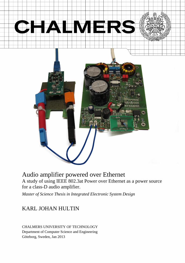
Cover: Photo of the PoE-amplifier prototype created in this project
Department of Computer Science and Engineering
Göteborg, Sweden, January 2013
Page 3
i
Acknowledgments
Acknowledgments
This master thesis has been carried out at Lab.gruppen AB,
Kungsbacka, Sweden. I would like to thank Klas Dalbjörn and
Fredrik Kihlberg for the supervision and for the opportunity to
realize an interesting project at Lab.gruppen.
I also would like to thank my supervisor Sven Knutsson at the
department of Computer Science and Engineering, Chalmers
University of Technology.
A special thanks to Bengt Johansson for the great feedback of the
report and to Harald Lüning for pushing me through the last part.
Page 5
iii
Abstract
Today, a professional amplifier may be supplied with its input as
well as control and monitoring via Ethernet. By Power over
Ethernet (PoE) it is now possible to provide its power as well. It
means that an amplifier can be fully operating with a single cable.
Power over Ethernet is standardized by IEEE and it allows 25-34
W to be distributed over a twisted-pair Ethernet cable.
As a proof of concept, a PoE amplifier is created and evaluated.
The performance of the amplifier is analyzed to determine if PoE
is suited for powering amplifiers. The amplifier is measured both
when it is powered over Ethernet and when it is powered with a
regular power supply unit. The result is compared to determine
what impact PoE has on the output audio quality.
The PoE amplifier is able to deliver 25 W of continuous output
power and it can deliver up to 81.8 W when playing a “music like”
signal with good audio quality. For lower level output there is no
impact in the audio quality on the PoE amplifier but for higher
output power the amplifier loses some of its linearity.
Page 6
iv
Table of contents
Acknowledgments ........................................................................................... i
Abstract ........................................................................................................... iii
Table of contents ........................................................................................... iv
Table of Figures ............................................................................................. vi
Abbreviations ................................................................................................ vii
1. Introduction .............................................................................................. 1
1.1 Background ............................................................................................. 1
1.1.1 Power over Ethernet ....................................................................... 1
1.2 Purpose ................................................................................................... 2
1.3 Approach ................................................................................................. 2
1.4 Limitation and delimitation ...................................................................... 3
2. Theory ....................................................................................................... 4
2.1 Power over Ethernet ............................................................................... 4
2.1.1 Power sourcing equipment .............................................................. 4
2.1.2 Powered Device .............................................................................. 5
2.1.3 Identifying Powered Devices ........................................................... 6
2.1.4 Classification of Powered Devices .................................................. 6
2.1.5 802.3at specifications ...................................................................... 7
2.2 Audio Measurements .............................................................................. 8
2.2.1 dBu .................................................................................................. 8
2.2.2 dBFS ............................................................................................... 8
2.2.3 Power .............................................................................................. 9
2.2.4 Total Harmonic Distortion .............................................................. 10
2.2.5 Total Harmonic Distortion plus Noise ............................................ 10
2.3 Class-D ................................................................................................. 10
2.3.1 Output stage .................................................................................. 11
2.3.2 Modulation ..................................................................................... 12
3. System design and Implementation .................................................... 14
3.1 Powered Device Interface ..................................................................... 15
3.2 Power good switch ................................................................................ 16
3.3 Current limiter ....................................................................................... 16
3.4 Capacitor bank ...................................................................................... 17
3.5 Output stage ......................................................................................... 18
3.6 Powering the system............................................................................. 19
3.7 Evaluation board ................................................................................... 19
3.8 IP block for converting audio signal to PWM signals ............................ 20
4. Test setup and test method .................................................................. 22
4.1 Power supply unit .................................................................................. 22
4.2 Power sourcing equipment ................................................................... 23
4.3 Audio analyzer ...................................................................................... 23
4.4 Load ...................................................................................................... 23
4.5 Test settings .......................................................................................... 24
Page 7
v
4.5.1 Linearity and continuous power .................................................... 24
4.5.2 Spectrum analysis ......................................................................... 24
4.5.3 THD+N .......................................................................................... 24
4.5.4 Burst power ................................................................................... 25
5. Results .................................................................................................... 26
5.1 Audio measurements ............................................................................ 26
5.1.1 Linearity ......................................................................................... 26
5.1.2 Continuous Power ......................................................................... 26
5.1.3 Burst Power ................................................................................... 28
5.1.4 Noise floor and THD+N ................................................................. 31
6. Discussion ............................................................................................. 35
6.1 Discussion of results ............................................................................. 35
6.2 How to use the amplifier ....................................................................... 38
6.2.1 Installation ..................................................................................... 38
6.2.2 Surveillance and emergency system ............................................ 41
6.2.3 Centralized Signal Processing and distributed amplification. ....... 42
6.3 Future work ........................................................................................... 42
6.3.1 Feedback loop ............................................................................... 42
6.3.2 More power than 25.5 W ............................................................... 43
7. Conclusion ............................................................................................. 44
8. References ............................................................................................. 45
Page 8
vi
Table of Figures
Figure 2.1 Schematic view of endpoint PSE and midspan PSE. ...................... 5
Figure 2.2 Half-bridge configuration. ............................................................... 11
Figure 2.3 H-bridge configuration. .................................................................. 12
Figure 2.4 PWM representation of the signal generated with a triangle wave.13
Figure 3.1 Block diagram over the PoE amplifier. .......................................... 15
Figure 3.2 A simplified schematic of the PD-interface .................................... 16
Figure 3.3 Simplified schematic of the switched current limiter. ..................... 17
Figure 3.4 Block diagram over the processing blocks in the FPGA. .............. 20
Figure 4.2 Block diagram over the test setup. ................................................ 22
Figure 5.1 Linearity. ........................................................................................ 26
Figure 5.2 Continuous output power. .............................................................. 27
Figure 5.3 Burst power. ................................................................................... 28
Figure 5.4 Output during one burst. Input 0 dBFS. ......................................... 29
Figure 5.5 Output during one burst. Input -1.75 dBFS. ................................... 30
Figure 5.6 Spectrum analysis for the non-PoE amplifer. ................................ 31
Figure 5.7 Spectrum analysis for the PoE amplifier. ....................................... 32
Figure 5.8 THD+N vs Input level, Input frq. 1 kHz. ......................................... 33
Figure 5.9 THD+N vs Input frequency, input level -15dBFS. .......................... 34
Page 9
vii
Abbreviations
AES Audio Engineering Society.
AES3 AES standard for serial transmission format for two-
channel linearly represented digital audio.
BPM Beats per minuets
dBFS Decibel full scale, referenced to the maximum of the
signal
dBu Decibel unit for voltage referenced to approximately
0.775 V
DSP Digital signal processor
DUT Device under test
EMI Electromagnetic interference
FET Field-effect transistor
FPGA Field Programmable Gate Array.
IEEE Institute of Electrical and Electronics Engineers.
PCM Pulse-code modulation
PD Powered Device
PoE Power over Ethernet.
PSE Power Sourcing Equipment
PSU Power Supply Unit
PTZ Pan, tilt and zoom. Type of camera.
PWM Pulse-width modulation
RMS Root mean square
THD Total harmonic distortion
THD+N Total harmonic distortion plus noise
TP Twisted-pair
UPS Uninterruptible power supply
Page 11
1
1. Introduction
1.1 Background
There are three essential elements in an amplifier. First, the
amplifier must have a power source that is capable of driving the
amplifier to the desired output power. Even if an amplifier can
have varying power sources like batteries for a handhold device or
be powered by the generator in the car, almost all amplifiers for
professional use are powered from the mains power grid.
Secondly, to have any output from the amplifier there must be an
input signal. There are a large variety of audio signal formats and
the pro audio market has not settled on a single standard. The most
commonly used formats in pro audio are balanced analog signal
and AES/EBU which is a digital format. Recently, audio over
Ethernet has started to evolve and also here there are a large
variety of solutions [1]. IEEE has a task group that is developing a
standard that is commonly called Audio Video Bridging which
would allow low latency audio and video to be transmitted over
Ethernet [2].
The third essential element of an amplifier is the ability to control
the amplifier. The most basic control of an amplifier is to adjust
the gain but some amplifiers also have the ability to, for example,
equalize and add delay to the signal and to set limiters on the
output. Most amplifiers have a physical control interface at the unit
but some also have the ability to be remotely controlled by, for
example, a computer or control panel, and this communication is
often based on Ethernet.
When both the audio signal and the control interface are evolving
towards Ethernet based solutions it would also be of interest to
have a power source that is based on Ethernet. Unifying parts of
the amplifier into one standardized and well known technology can
bring simplicity to the user. Having power, control, and audio
signal all transmitted over Ethernet, would give an amplifier that
only needs one single cord to operate.
1.1.1 Power over Ethernet
Power over Ethernet (PoE) is a technology to provide power over a
standard Ethernet cable. The idea of PoE is to be able to power
Page 12
2
network devices on the same network that the device uses for
communication. PoE has been included in the IEEE 802.3 Ethernet
standard since 2003 [3]. The last update of the standard makes sure
that 25.5 W can be provided on an Ethernet network [4].
1.2 Purpose
An audio amplifier that is powered over Ethernet and that has both
control and audio over the network has the advantage of only
requiring a single cord to operate. This is especially interesting for
amplifiers suited for installation, because the need of new wiring is
minimized. Furthermore, by being compliant with the IEEE
standards, it will be simple to connect an amplifier to an existing
network or to build a network of “off-the-shelf” products.
For this type of amplifier, it is important to limit the physical size
of the product to make it easier to fit the amplifier in an installation.
It is also important to have high efficiency since the power that can
be distributed over Ethernet is limited. A class D amplifier has
both the benefit of reduced size and weight and has a high
efficiency compared to other common types of amplifiers [5].
Within this thesis the concept of an amplifier that is powered over
Ethernet is proven. It is done by constructing a prototype of a PoE
amplifier. The focus is on the PoE part of the amplifier. The main
challenges is to design a power supply unit (PSU) that fulfills the
IEEE 802.3at standard without exceeding the power limit of
25.5 W [4] and that at the same time can drive the amplifier with a
peek output power of 100+ W with good sound quality.
Furthermore, the applications of a PoE-amplifier are investigated.
It is compared to the system installation solutions of today and
new applications that fit PoE-amplifiers well are presented.
1.3 Approach
A prototype is constructed to prove the concept of a PoE-amplifier.
The prototype had the requirements to use technology that could
be used in a consumer product in the sense of low price, small size
and energy efficiency. It also had the requirement to comply to the
IEEE standard for PoE which would make it compatible with other
PoE equipment.
The prototype is a further development of an existing prototype of
a medium power, class-D amplifier. The amplifier has a full-bridge
Page 13
3
output stage which basically consists of four transistors packed
into a single chip. (See section 3.5 for more details.) The full-
bridge is driven with pulse width modulated (PWM) signals which
are generated by an FPGA and the input signal to the FPGA comes
from an S/PDIF interface.
The prototype is constructed in such a way that the PoE module
can easily be bypassed which means that the amplifier can be
directly powered by an external power supply. This makes it
possible to compare the same amplifier when it is powered over
Ethernet and when it is power in a regular way and to determine
the impact of PoE on the amplifier.
1.4 Limitation and delimitation
Even if the biggest advantage of a PoE-amplifier is to be able to
operate with a single cable, this thesis will not go into details about
audio over Ethernet or monitoring/control over Ethernet. Nor will
the constructed prototype support audio or monitor/control over
Ethernet.
Unlike a final product, the entire prototype is not powered over
Ethernet. The FPGA and its peripheral circuitry are powered by a
five volt power supply. But the output stage of the amplifier is
powered over Ethernet so the power for the output signal comes
from PoE.
When the usage of the PoE amplifier is discussed it is only done in
the scope of professional usage and not for consumer usage. The
focus is on the installation application.
Page 14
4
2. Theory
2.1 Power over Ethernet
The PoE standard specifies how power can be provided on an
Ethernet network without interfering with the data communication
in a safe way.
It also specifies a protocol to detect devices that requests power
and a method to dynamically negotiate the power needs. This
implies that devices which are not compatible with PoE are not fed
with power that can damage the device. Therefore, non-PoE
devices and PoE devices can coexist in the same network without
disturbing each other. If a powered Ethernet cable is disconnected
the power is immediately cut and it makes the system safe and
prevents electrical shocks [4].
The early IEEE 802.3af standard can guarantee that 12.95 W reach
the unit that requested power [3]. The new IEEE 802.3at standard,
which was published in September 2009, extends the allowed
power to 25.5 W in the receiving end [4]. The extra power makes
it possible not only to power small cameras, IP-telephones and
wireless access points but also to power more power consuming
products like pan-tilt-zoom cameras, displays, small computers
and to be used in emergency power grids.
The following sections (2.1.1 to 2.1.5) are all referred to IEEE
standard 802.3at [4] unless otherwise stated. Some parts have
references to specific sections in the IEEE standard 802.3at and
they are written within parentheses.
2.1.1 Power sourcing equipment
The unit that is supplying power to an Ethernet cable is called
power sourcing equipment (PSE) and the unit that is receiving
power is called powered device (PD). In a twisted-pair (TP) cable
used for Ethernet, there are four wire pairs and two or four pairs
are used for the data link layer depending on the Ethernet
implementation that is used. The PSE may provide power on two
of the four wire pairs. In a standard Ethernet TP cable, the power
must be provided over either pair 1/2 and 3/6 or over pair 4/5 and
7/8 but it is up to the PSE to decide which pairs to use.
Page 15
5
The PSE does not affect the data link since the data is transmitted
by differential mode within the pairs and the PSE provides power
in common mode to one pair and thereby creating a potential
difference between the pairs.
The main functions of the PSE, as described in the IEEE 802.3at
standard, are as follows:
To search the link section for a PD
To supply power to the detected PD through the link section
To monitor the power on the link section
To remove power when no longer requested or required,
returning to the searching state
The PSE can be placed in two different locations relative to the
cable. It can be merged together with the unit that is using the data
link layer and then it is called an Endpoint PSE. This can for
instance be a switch or a hub. The PSE can also be placed in
between the units using the data link layer and inject power to the
cable without dealing with the data and then it is called an
Midspan PSE.
PDPSE
Data Pair
Data Pair
Data Pair
Data Pair2
3
4
5
6
7
8
1
2
3
4
5
6
7
8
1
PoE Switch Powered unit
Data Pair
Data Pair 2
3
4
5
6
7
8
1
Non-PoE Switch
PD
Data Pair
Data Pair2
3
4
5
6
7
8
1
Powered unit
PSE
Midspan Power injector
Figure 2.1 Schematic view of endpoint PSE and midspan PSE.
2.1.2 Powered Device
A PD must be able to identify itself as a PD to receive power from
the PSE. It must also be able to negotiate its power need with the
PSE.
Page 16
6
Since it is the PSE that decides which pairs in a TP-cable that
should be powered, the PD must be able to receive power in both
alternatives. The TP-cable can also be crossed over and therefore
the power must be full wave rectified at the PD to ensure the
polarity.
2.1.3 Identifying Powered Devices
The PSE must identify the device on the network as a PD before a
power connection can be established. The PSE is searching for
PDs by probing for a signature resistor of 25 kΩ at the powered
wire pair. The PSE shall make at least two measurements at
different voltages in the range of 2.8 V to 10.0 V. The effective
resistance calculated by equation (2.1) must be in the range of
19.0 kΩ to 26.5 kΩ. (IEEE 802.3at-2009, 33.2.5)
(2.1)
Where V1 and V2 are the probing voltages for the first and second
measurement and where I1 and I2 are the measured current. R is the
effective resistance.
2.1.4 Classification of Powered Devices
The PD must be classified in order to determine the power
requirements of the PD. This is done so that a PSE, with many PoE
ports but a limited total available power, can know how much each
PD is requesting and deny further PDs when the limit of the total
power is reached.
There are four fixed power classes the PD can request. Table 1
shows the classes and the maximum power at the PSE and the
guaranteed power at the PD.
Class Maximum
power at PSE
Power at
PD
Nominal Signature
load current
0 15.4 W 12.95 W < 4.00 mA
1 4.00 W 3.84 W 10.5 mA
2 7.00 W 6.49 W 18.5 mA
3 15.4 W 12.95 W 28.0 mA
4 30.0 W* 25.5 W* 38.0 mA
* Only used in IEEE 802.3at, otherwise equal to class 0.
Table 1: Power classes in 802.3af and 802.3at
Page 17
7
The method for communicating the classification from the PD to
the PSE is used in the older IEEE 802.3af standard and it is called
1-event classification. This method got extended in IEEE 802.3at
into the 2-event classification. It is backwards compatible so that
PD and PSE from both standards can be mixed.
In both 1-event and 2-event, the PSE is probing for the
classification by applying a voltage in the range of 14.5 V to
20.5 V and the PD signals the desired power classification by
drawing a specific load current. The load currents can be found in
Table 1. The PD knows if it is probed for identification (see 2.1.3)
or if it is probed for classification since the probing is done in
different voltage ranges.
What distinguishes 2-event from 1-event classification is that in
the 2-event classification, the PSE is probing two times with a
mark voltage in between. If the PD responds correctly to the mark
state and the second probing, the PSE knows that the PD is
supporting the newer 802.3at standard. And the other way around,
if a PD sees a 2-event probing, it knows that the PSE is of standard
802.3at. In the mark state the PSE is applying a voltage in the
range of 7.0 V to 10.0 V and the PD should response by drawing a
load current between 0.25 mA and 4.00 mA.
The 802.3at standard also introduces another method for
classification. It uses the data layer and sends a data packet with
the requested power. This gives the possibility to specify a much
more specific desired power in steps of 0.1 W. It also gives the
PSE and PD the ability to dynamically negotiate the power needs
and exchange other information like: power priority, if the PD has
an auxiliary power supply or if the PSE is running on backup
power.
2.1.5 802.3at specifications
The following specifications are only a part of the specifications in
the IEEE 802.3at. These specifications are the most essential or
important for this project.
The power that can be distributed over Ethernet is limited by an
maximal current which depends on the classification. The highest
classification has a current limitation of 600 mA. This value has
been specified with respect to the capacity of a CAT5 cable and
Page 18
8
that it should withstand the heat generated due to losses in the
cable (IEEE 802.3at-2009, 33.1.4). The PSE may cut the power if
the PD draws more current than it has been classified for but the
PD is also allowed to exceed the classified power for a short time.
This peak power is about 11% over the classified power and it can
be drawn for 50 ms. This can be repeated with a duty cycle of 5%
(IEEE 802.3at-2009, 33.3.7.4).
The output voltage from the PSE (VPort_PSE) can be in the range of
50 V to 57 V. The input voltage at the PD (VPort_PD) is allowed to
drop down to 42.5 V due to losses in cables. The PSE may turn off
the power if VPort_PSE drops below 50 V. The PD may turn off if
VPort_PD is below 42.5 V and must turn off if VPort_PD gets below
30 V. (IEEE 802.3at-2009, 33.2.7, 33.3.7)
The result is that an 802.3at PSE must have a minimum power
output of 30 W (50 V * 600 mA) but the maximum power can be
up to 34.2 W (57 V * 600 mA) and that the PD are guaranteed an
input power of 25.5 W (42.5 V * 600 mA) but the power can be as
high as 34.2 W under ideal circumstances.
During power up state, the inrush current should be limited to
450 mA by the PSE (IEEE 802.3at-2009, 33.2.7.5). When the PD
has reached the power on state, it must keep the power
consumption low for another 80 ms to allow the PSE to switch
from power up to power on state. ( IEEE 802.3at-2009, 33.3.7.3)
2.2 Audio Measurements
2.2.1 dBu
dBu is a voltage-based decibel unit referred to 0.7746 V and it is a
unit commonly used in professional audio and broadcast industry.
The reference is derived from the fact that with this voltage 1 mW
is dissipated when the load is 600 Ω [6]. This is remains from old
technology when it was important to have matching output
impedance with the input impedance of the next device and 600 Ω
was the standard.
2.2.2 dBFS
dBFS stands for decibel full scale and it is commonly used for
amplitude level in digital systems. 0 dBFS is the highest possible
Page 19
9
value in a given digital representation. Therefore, all dBFS
measurements must be zero or below.
2.2.3 Power
The output power of an amplifier is the power that drives the
speakers and it can be measured by looking at the output root
mean square (RMS) voltage over a known load. Specifying the
output power of an amplifier can be done in many ways and there
is no perfect way to do it. The problem is that the output power of
an amplifier that is designed for audio should be specified by a
signal similar to audio. But since audio can be anything from one
single tone to speech and music there is no such signal. Also, to be
able to compare different amplifiers with each other there must be
a simple way to recreate the signal. The output power of the
amplifier in this project is shown in two ways.
Continuous power is measured with an input signal that is a
1 kHz sine wave signal at a level such that the amplifier is not
clipping and has a low harmonic distortion. The load is purely
resistive and it has an impedance of 8 Ω. The measurement is done
over several minutes. This measurement does not represent audio
very well but it gives an indication of what the amplifier is capable
of and it is very easy to compare with tests of other amplifiers.
“12 dB burst” is a signal that has an energy content which is
similar to music. The input signal is a 1 kHz sine wave with a part
with high amplitude and a part with low amplitude. The high part
last for 25 ms and it is followed by the low part for 375 ms that
together gives a crest factor (peak-to-average ratio) of 12 dB.
(2.2)
To get a crest factor of 12 dB with the given times for the high and
low parts above, the low part must have an amplitude that is 25.8%
or of the amplitude of the high part
The signal is repeated for a long time. The signal can be seen as
music with a bass beat at 150 BPM. The 25 ms peak has the same
energy content as one period of a 40 Hz sine wave.
It is possible to drive a signal that has a higher output power than
the maximum continuous power if the amplifier has a capacitor
Page 20
10
bank that stores energy. In the beginning of the peak when the
capacitor bank is fully charged the output might be as high as
expected but if the output from the bank is higher than the input
the stored energy will decrease and the output peak will lose
amplitude. One may say that the signal decays and it can be
represented by the factor of the damping from the beginning to the
end of the peak.
The output power is measured for the RMS voltage of the peak
when the amplifier is loaded with 8 Ω purely resistive load. Also
the harmonic distortion and the decay are observed during the
measurement.
2.2.4 Total Harmonic Distortion
Total harmonic distortion (THD) is a measurement of the
harmonic tones that appears at integer multiples of the frequency
of the fundamental tone. This is an unwanted disturbance added by
the amplifier and it is desirable to keep it as low as possible. The
THD is defined as the RMS voltage of all overtones, divided by
the fundamental tone as in equation (2.3) [7].
(2.3)
2.2.5 Total Harmonic Distortion plus Noise
It is hard to measure each individual harmonic in a signal and
distinguish the harmonics from other noise. Therefore another way
of measuring the distortion is more commonly used. Instead of
trying to distinguish each harmonic from the noise, both the
harmonics and the noise are compared with the fundamental signal
and this is called Total Harmonic Distortion plus Noise (THD+N).
THD+N is measured by applying a fundamental signal to the
amplifier and then applying a notch filter on the output that
removes the fundamental signal. The outputs with and without the
fundamental signal is compared to get the THD+N ratio [7].
2.3 Class-D
A class D amplifier is also called a switching amplifier. The name
comes from the fact the output stage is not operating in linear
mode but instead is using switches to turn the power to the load
fully on or off at a high rate.
Page 21
11
There are several steps of signal processing in a class D amplifier.
The input audio signal is encoded into a stream of pulses where the
width of the pulse is representing the signal’s amplitude. This is
called pulse width modulation (PWM) and it is described in
section 2.3.2. The PWM signals are driving the output stage and
the output signal is low-passed filtered to recreate the desired
signal.
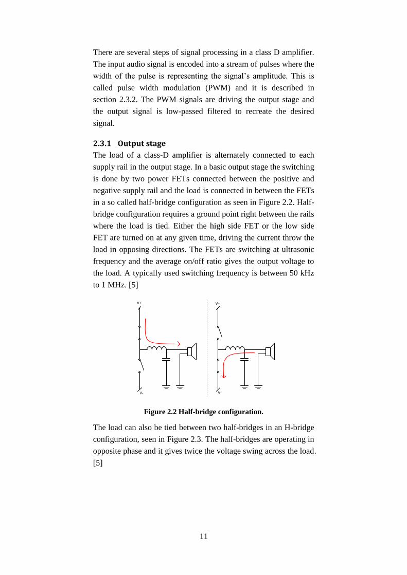
2.3.1 Output stage
The load of a class-D amplifier is alternately connected to each
supply rail in the output stage. In a basic output stage the switching
is done by two power FETs connected between the positive and
negative supply rail and the load is connected in between the FETs
in a so called half-bridge configuration as seen in Figure 2.2. Half-
bridge configuration requires a ground point right between the rails
where the load is tied. Either the high side FET or the low side
FET are turned on at any given time, driving the current throw the
load in opposing directions. The FETs are switching at ultrasonic
frequency and the average on/off ratio gives the output voltage to
the load. A typically used switching frequency is between 50 kHz
to 1 MHz. [5]
V+V+
V- V-
Figure 2.2 Half-bridge configuration.
The load can also be tied between two half-bridges in an H-bridge
configuration, seen in Figure 2.3. The half-bridges are operating in
opposite phase and it gives twice the voltage swing across the load.
[5]
Page 22
12
Vrail Vrail Vrail Vrail Vrail Vrail
Figure 2.3 H-bridge configuration.
2.3.2 Modulation
The input signal must be modulated into a stream of pulses and it
can be done in many ways. The most commonly used modulation
in a class D amplifier is pulse width modulation (PWM). The
width of the pulse corresponds to the amplitude of the audio signal.
The pulses have a much higher frequency (typically 50 kHz to 1
MHz) than the audio signal and they are outside the hearable range
for a human.
Conceptually, the PWM signal is generated by comparing the
audio signal to a ramp or triangular waveform running at a carrier
frequency higher than audio range. As seen in Figure 2.4, if the
input signal is higher than the triangular waveform, the PWM
signal is high and if the input signal is lower than the triangle
waveform, the PWM signal is low.
Page 23
13
Figure 2.4 PWM representation of the signal generated with a
triangle wave.
A large positive input signal corresponds to a duty cycle of near
100% and a large negative input corresponds to near 0%. For a
silent audio signal, when the signal is 0, the duty cycle will be 50%.
In other words, the output will be switching in full speed even
when the desired output signal is 0. An amplifier with PWM has a
high electromagnetic interference (EMI) at the carrier frequency.
[5] [8]
There is a variant of PWM called three-level or three-state PWM.
The output stage must be an H-bridge to use three-level PWM.
The three states are one positive state when one half-bridge is
driving the current in positive direction through the load and one
negative state when the other half-bridge is driving the current in
the negative direction. In the third neutral state both half-bridges
are grounded and no current is drawn from the rail. Three-level
PWM have a little higher efficiency since no power is drawn in the
neutral state and since the switch losses are less because it is only
one transistor switching at any given time. It has also a little less
EMI. [8]
Page 24
14
3. System design and Implementation
To prove the concept of an amplifier that is powered over Ethernet
a prototype of a PoE amplifier is developed. The amplifier that is
designed within this project is a further development of an existing
prototype for a class D amplifier. This prototype was developed by
the company TC Electronics in Denmark as an investigation of a
FPGA based class D amplifier.
The earlier prototype consists of an output stage board with a
single-chip full bridge which is mounted on an evaluation board
for a Virtex 4 FPGA from Xilinx. It is the FPGA that controls the
full bridge and it is done with the help of an IP block that converts
the incoming audio signal to a PWM signal. The evaluation board
and the IP block are reused in the development of the new
amplifier and the output stage board is redesigned to have a full
bridge with higher voltage rating and whereby make it possible to
be powered over Ethernet.
The main blocks, beside the full-bridge on the new board created
in this project, are a PD interface that establishes the powered
connection to the PSE, a “power good” switch that keeps the
amplifier turned off until the powered connection is established, a
current limiter that ensures that the maximum allowed current is
not exceeded and a capacitor bank that stores energy which makes
it possible to have a much higher burst output power than the
maximum input power. Figure 3.1 shows a block diagram of the
amplifier and its most significant parts.
Page 25
15
PDInterface
Full Bridge
Current limiter
FPGAPWM
Rectifying Bridge
Ethernet Port with Magnetics
Power
Data
+
-
Vrail
Energy storage
Load
Digital Audio
PoE
Figure 3.1 Block diagram over the PoE amplifier.
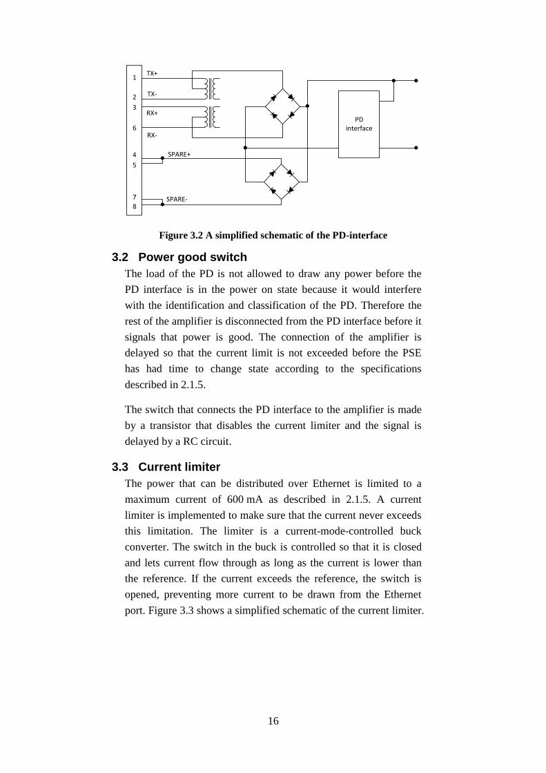
3.1 Powered Device Interface
To use PoE a PD interface is implemented. The purpose of the PD
interface is to establish a connection to a PSE that can power the
amplifier. The PD interface is built around a single chip device
from Linear Technology called LTC4265 [9]. The device is a PD
interface controller that meets the requirements of the IEEE802.3at
standard. It takes care of the identification of the PD and it
responds to the classification request from the PSE.
When power is provided at the Ethernet port, the LTC4265 has a
smooth power-up transition that limits inrush current and a “power
good”-signal is raised when the power is valid and the PD has
entered the power on state. [9]
Beside the interface controller, the PD interface has a connector
for a twisted-pair cable. The connector has isolation transformers
with center taps for separating the DC power from the differential
data link communication.
The PD interface also has two rectifying diode bridges to ensure
the polarity even when a crossed over cable is used.
Figure 3.2 shows a simplified schematic of the PD interface used
in this project.
Page 26
16
PDinterface
1
2
3
6
4
5
7
8
TX+
TX-
RX+
RX-
SPARE+
SPARE-
Figure 3.2 A simplified schematic of the PD-interface
3.2 Power good switch
The load of the PD is not allowed to draw any power before the
PD interface is in the power on state because it would interfere
with the identification and classification of the PD. Therefore the
rest of the amplifier is disconnected from the PD interface before it
signals that power is good. The connection of the amplifier is
delayed so that the current limit is not exceeded before the PSE
has had time to change state according to the specifications
described in 2.1.5.
The switch that connects the PD interface to the amplifier is made
by a transistor that disables the current limiter and the signal is
delayed by a RC circuit.
3.3 Current limiter
The power that can be distributed over Ethernet is limited to a
maximum current of 600 mA as described in 2.1.5. A current
limiter is implemented to make sure that the current never exceeds
this limitation. The limiter is a current-mode-controlled buck
converter. The switch in the buck is controlled so that it is closed
and lets current flow through as long as the current is lower than
the reference. If the current exceeds the reference, the switch is
opened, preventing more current to be drawn from the Ethernet
port. Figure 3.3 shows a simplified schematic of the current limiter.
Page 27
17
Rsense
+
-
+
-
Vcc
Vcc/2
Vcc
Gate driver
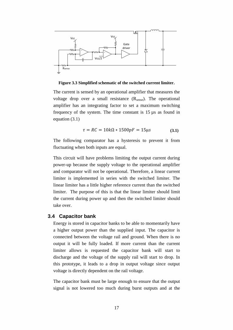
Figure 3.3 Simplified schematic of the switched current limiter.
The current is sensed by an operational amplifier that measures the
voltage drop over a small resistance (Rsense). The operational
amplifier has an integrating factor to set a maximum switching
frequency of the system. The time constant is 15 µs as found in
equation (3.1)
(3.1)
The following comparator has a hysteresis to prevent it from
fluctuating when both inputs are equal.
This circuit will have problems limiting the output current during
power-up because the supply voltage to the operational amplifier
and comparator will not be operational. Therefore, a linear current
limiter is implemented in series with the switched limiter. The
linear limiter has a little higher reference current than the switched
limiter. The purpose of this is that the linear limiter should limit
the current during power up and then the switched limiter should
take over.
3.4 Capacitor bank
Energy is stored in capacitor banks to be able to momentarily have
a higher output power than the supplied input. The capacitor is
connected between the voltage rail and ground. When there is no
output it will be fully loaded. If more current than the current
limiter allows is requested the capacitor bank will start to
discharge and the voltage of the supply rail will start to drop. In
this prototype, it leads to a drop in output voltage since output
voltage is directly dependent on the rail voltage.
The capacitor bank must be large enough to ensure that the output
signal is not lowered too much during burst outputs and at the
Page 28
18
same time, it can’t be so large that it is not fully recharged between
two burst outputs.
The PoE amplifier is designed to handle burst outputs as described
in section 2.2.3. The capacitor bank was chosen to be 9600 µF and
it was found using the following approximation:
An acceptable voltage drop would be 6 volt. If the rail voltage is
50 V then the max peak output voltage would be 25 V. If the load
is 8 Ω then the maximum output current can be 2.2 A found in
(3.2).
√ (3.2)
And
⇒
(3.3)
9600 µF was chosen instead of 9100 µF since it was easier to find
that component value.
3.5 Output stage
The output stage is a full-bridge configuration with dual power
FETs at each node. The full-bridge is integrated in a single chip
called STA516b manufactured by STMicroelectronics [10]. The
chip has four power half-bridges which can be configured to either
drive four channels in half-bridge mode or two channels in full-
bridge mode. It can also be configured to combine the two full-
bridge channels into one channel with dual half-bridges on each
side of the load which means that twice the current can pass
through the nodes.
STA516b has an input to each of the four half-bridges. This gives
a high degree of freedom for the designer to control the output
stage but in the same time, special care must be taken not to drive
the output stage into a bad state that can permanently damage the
circuit. The output stage can be driven by both regular PWM
signals and tree-level PWM.
Page 29
19
STA516b has protections for under-voltage, thermal and over-
current. The protection shuts down the circuit and puts the outputs
in high impedance mode if a fault occurs. [10]
In this amplifier the STA516b output stage is configured to run as
one channel with dual half-bridges on each side of the load. It is
driven from the FPGA with either a regular PWM signal or a
three-level signal that can be selected by a switch but for all results
in this report a three-level signal is used.
3.6 Powering the system
The connection from the output of the current limiter to the
capacitor bank is made so that it can easily be opened and thereby
separating the PD and current limiter on one side and the capacitor
bank and whole output stage on the other. This makes it possible to
choose if the amplifier should be powered over Ethernet or if an
external power supply should be connected directly to the
capacitor bank and the output stage.
In a final product the whole system would be powered over
Ethernet but in this prototype some parts are powered from another
source than PoE. The whole evaluation board containing the
FPGA and its surrounding components is powered by a separate 5
V PSU. See section 4.1.
3.7 Evaluation board
The evaluation board consists of a Virtex 4 FPGA from Xilinx and
a flash memory to configure the FPGA on power up.
The board also contains:
Power supply unit
Sample rate converter
196MHz clock generator
AES receiver
RS-232 interface
#40 Pin Head
Inputs and outputs:
RCA for S/PDIF input
2 x TOSLINK for optical tx / rx
BNC for world clock generation
Page 30
20
#100 pin connector for mounting an extension board, in this
case, an output stage board.
User interface:
20 x double colored LEDs
16 x DIP switches
2 x adjustment knobs
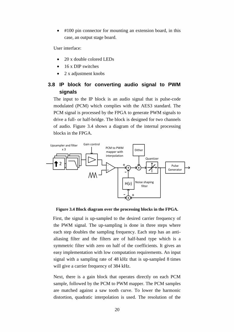
3.8 IP block for converting audio signal to PWM
signals
The input to the IP block is an audio signal that is pulse-code
modulated (PCM) which complies with the AES3 standard. The
PCM signal is processed by the FPGA to generate PWM signals to
drive a full- or half-bridge. The block is designed for two channels
of audio. Figure 3.4 shows a diagram of the internal processing
blocks in the FPGA.
+
+
H(z)
-+
- +
2 2Pulse
Generator
2
Upsampler and filterx 3
Gain control
Quantizer
+
Dither
-
+
Noise shaping filter
PCM to PWM mapper with interpolation
Figure 3.4 Block diagram over the processing blocks in the FPGA.
First, the signal is up-sampled to the desired carrier frequency of
the PWM signal. The up-sampling is done in three steps where
each step doubles the sampling frequency. Each step has an anti-
aliasing filter and the filters are of half-band type which is a
symmetric filter with zero on half of the coefficients. It gives an
easy implementation with low computation requirements. An input
signal with a sampling rate of 48 kHz that is up-sampled 8 times
will give a carrier frequency of 384 kHz.
Next, there is a gain block that operates directly on each PCM
sample, followed by the PCM to PWM mapper. The PCM samples
are matched against a saw tooth curve. To lower the harmonic
distortion, quadratic interpolation is used. The resolution of the
Page 31
21
PWM signal is limited by the clock speed of the system. This
system has a 9 bits resolution for the PWM signal which requires a
system clock of 196.608 Mhz (384 kHz * 2^9).
The quantization of the signal to 9 bits resolution introduces
quantization noise. With the help of a 5th order noise shaping filter
the quantization noise is pushed outside of the hearable range for a
human. Dithering is used to get rid of the cyclic and repeating
noise from quantization with otherwise appears as unpleasant
distortion. Dithering means that a random noise is added to the
quantization noise with basically distributes the noise more evenly.
Finally, there is a pulse generator block that has the ability to both
output a standard binary PWM signal and three-level PWM signal
to the output stage.
Page 32
22
4. Test setup and test method
To measure and compare the amplifier when it is powered over
Ethernet to when it is powered with an external power supply a set
of equipment is used. This section will describe the equipment and
the setup used. Figure 4.1 shows a block diagram of the test setup.
PSU
PSE
52.2 V 51.6 V
5.0 V
Audio InS/PDIF
DUT LoadAudio Out
Audio AnalyzerGen Aly
Power Cables
Ethernet TP-cable
Signal Cable
Figure 4.1 Block diagram over the test setup.
4.1 Power supply unit
A laboratory power supply is used to power the device under test
(DUT). The PSU used is called HM7042-5 produced by Hameg.
The PSU has three separate adjustable outputs. Two outputs which
can deliver up to 30 V at 2 A and one that can deliver up to 5.5 V
at 5 A.
According to the specification of PoE as described in section 2.1.5
the output voltage from the PSE is 50 to 57 V and to get that level
from the PSU the two “30 V” outputs are connected in series
which give a maximum of 60 V. Throughout all tests and
measurements in this thesis the output level from the PSU is
adjusted so that the rail voltage (Vrail in Figure 3.1 Block diagram
over the PoE amplifier.Figure 3.1) is 50.0 V. It means that when
the amplifier is powered over Ethernet the output voltage from the
PSU is 52.2 V which gives 51.6 V at the input of the PD interface.
When the amplifier is powered directly from the PSU without PoE,
the output from the PSU is 50.1 V.
Page 33
23
The third output of the PSU is used to power the evaluation board
with the FPGA and its surrounding components. It is adjusted to
output 5.0 V.
4.2 Power sourcing equipment
The PSE used in the test setup is an evaluation board of the
component Si3461 which is a single-port 802.3at PoE PSE
Interface manufactured by Silicon Labs [11].
The evaluation board (Si3461-EVB) has connectors for easy
connection to the PSU and it can be configured to run both as a
midspan and endspan PSE (see section 2.1.1). It is configured as
an endpoint in this project since there is no need of data transfer
over Ethernet.
4.3 Audio analyzer
An audio analyzer is used to both generate the test stimulus in the
form of audio signals and to analyze the performance of the
amplifier by sampling the output.
The output from the audio analyzer is in S/PDIF format and it can
be controlled with very high accuracy both for magnitude and
frequency and the output from the amplifier can be analyzed by an
analog analyzer with high precision. When the generator and
analyzer are acting together the audio analyzer is capable of
measuring linearity, measuring output power, do a spectrum
analysis and measure THD+N among other things. The audio
analyzer also has scripting abilities that makes it possible to make
advanced tests as measuring the burst output power.
The audio analyzer used is produced by Audio Precision and it’s
called 2722.
4.4 Load
Instead of a real speaker for loading the system, a dummy load is
used. The dummy load is basically a huge amount of effect
resistors connected in a grid which makes a load that can sink over
1000 W. The dummy load is purely resistive and the resistance can
be selected by a switch to be 2 Ω, 4 Ω, 8 Ω or 16 Ω. For all tests in
this thesis the load is 8 Ω if otherwise not stated.
Page 34
24
4.5 Test settings
The basic setup for all tests is that the input to the amplifier is from
the digital signal generator of the audio analyzer. The output of the
amplifier is connected to the dummy load of 8 Ω and the analog
analyzer is connected in parallel measuring the voltage over the
load.
4.5.1 Linearity and continuous power
The input level is swept from -50 dBFS to 0 dBFS with a step size
of 0.5 dB which gives 101 measurement points. The whole sweep
takes about 4 seconds. The output voltage is measured and with
the given load the analyzer is able to calculate the output power.
4.5.2 Spectrum analysis
The output the signal is analyzed with fast Fourier transform (FFT)
to find the frequency spectrum. The output is sampled at 48 kHz
and the length of the FFT is 4096 samples. It gives 2048 bins and
the distance between two bins is 23.44 Hz given by (4.1).
(4.1)
The spectrum of the output is measured at -40, -20, -10 and
0 dBFS.
4.5.3 THD+N
To find the THD+N the measured output signal is passed through a
notch filter that rejects the fundamental component. The notch
filter center frequency is automatically following the strongest
component in the signal. THD+N is the ratio between the sum of
the distortion products and the noise amplitude relative the
unfiltered signal.
The THD+N is measured in relation to input amplitude of the
fundamental signal and in relation to the input signal frequency.
For THD+N in relation to amplitude, the input frequency is fixed
at 1 kHz sine wave and the amplitude is swept from 0 dBFS down
to -50 dBFS with a step size of 1 dB. For THD+N in relation to
frequency the input level is -15 dBFS and the input frequency is
swept from 20 kHz down to 20 Hz at a total number of 120 points.
Page 35
25
4.5.4 Burst power
A custom made script is used to measure the burst power. The
input signal is the “12 dB-burst” signal described in section 2.2.3.
The signal has a short high part and a longer lower part where the
amplifier can recover. The script starts with measuring the gain of
the amplifier. It is done at a low signal level and it is used to
calculate the expected power from the amplifier. Next, the script
will increase the input level in steps. For each step it isolates the
high part and measures the voltage and calculates the power with
help of the known load. Both the average power of the peak and
the power of the first part of the peak are found.
The script can be run in a mode where a maximum allowed drop
from the early power to the average power is specified and the
script will find the input level with that drop by a successive
approximation method.
The script also finds the high part of the signal which can be used
to show how the signal is losing strength throughout the peak.
Page 36
26
5. Results
5.1 Audio measurements
5.1.1 Linearity
The linearity of the output power is measured by applying a
continuous 1 kHz sine wave at a varying amplitude and measure
the output RMS voltage when the amplifier is driving an 8 Ω
resistive load. The rail voltage is 50 V. The result is shown in
Figure 5.1. The x–axis is the input signal in dBFS and y-axis is the
output voltage in dBu.
Figure 5.1 Linearity.
The teal colored curve shows the linearity for the PoE amplifier
and the violet colored curve shows the linearity for the amplifier
powered by an external power supply.
5.1.2 Continuous Power
Continuous output power is measured with the same setup as for
linearity measuring. On the x-axis is the input level as dBFS and
on the Y-axis is the output power in W. The output power is found
by measuring the output voltage and taking it in relation to the
known and fixed 8 Ω resistive load.
Page 37
27
Figure 5.2 Continuous output power.
The teal colored curve shows the continuous output power for the
PoE amplifier and the violet colored curve shows the output power
for the amplifier with an external power supply.
Page 38
28
5.1.3 Burst Power
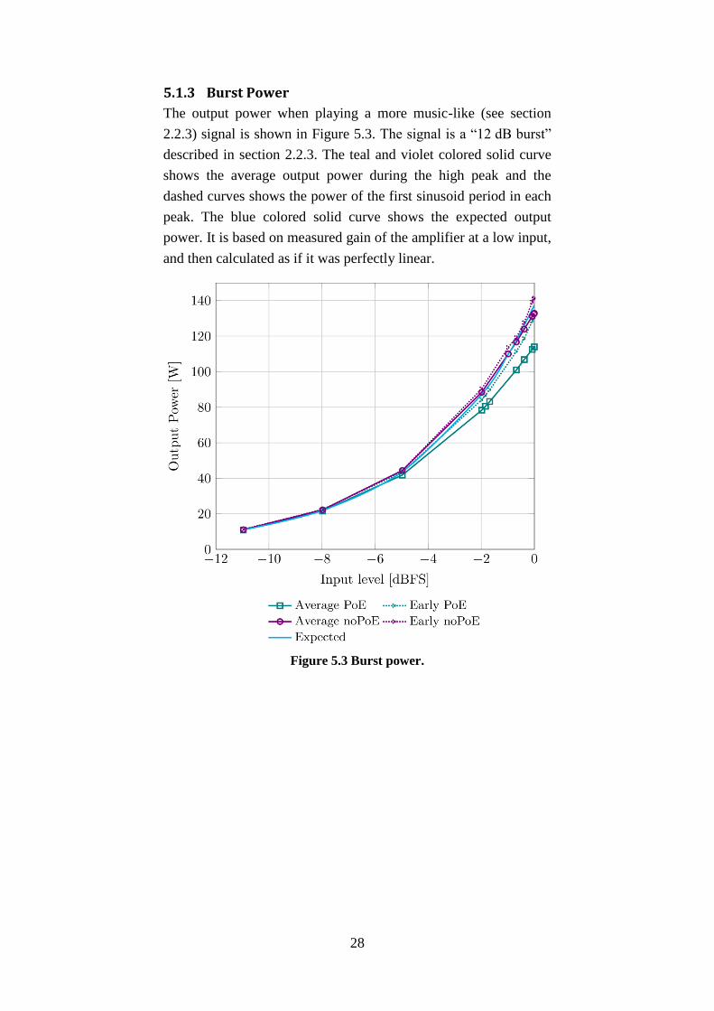
The output power when playing a more music-like (see section
2.2.3) signal is shown in Figure 5.3. The signal is a “12 dB burst”
described in section 2.2.3. The teal and violet colored solid curve
shows the average output power during the high peak and the
dashed curves shows the power of the first sinusoid period in each
peak. The blue colored solid curve shows the expected output
power. It is based on measured gain of the amplifier at a low input,
and then calculated as if it was perfectly linear.
Figure 5.3 Burst power.
Page 39
29
When playing a peak that has higher output than the maximum
continuous power the output will decay as the rail voltage drops.
As seen in Figure 5.3 the output power of the early part of the peak
is much higher than the average. Figure 5.4 and Figure 5.5 shows
how the peak loses strength when the stored energy decreases in
the capacitor bank. The x–axis is time and the y-axis is output
voltage.
Figure 5.4 Output during one burst. Input 0 dBFS.
Page 40
30
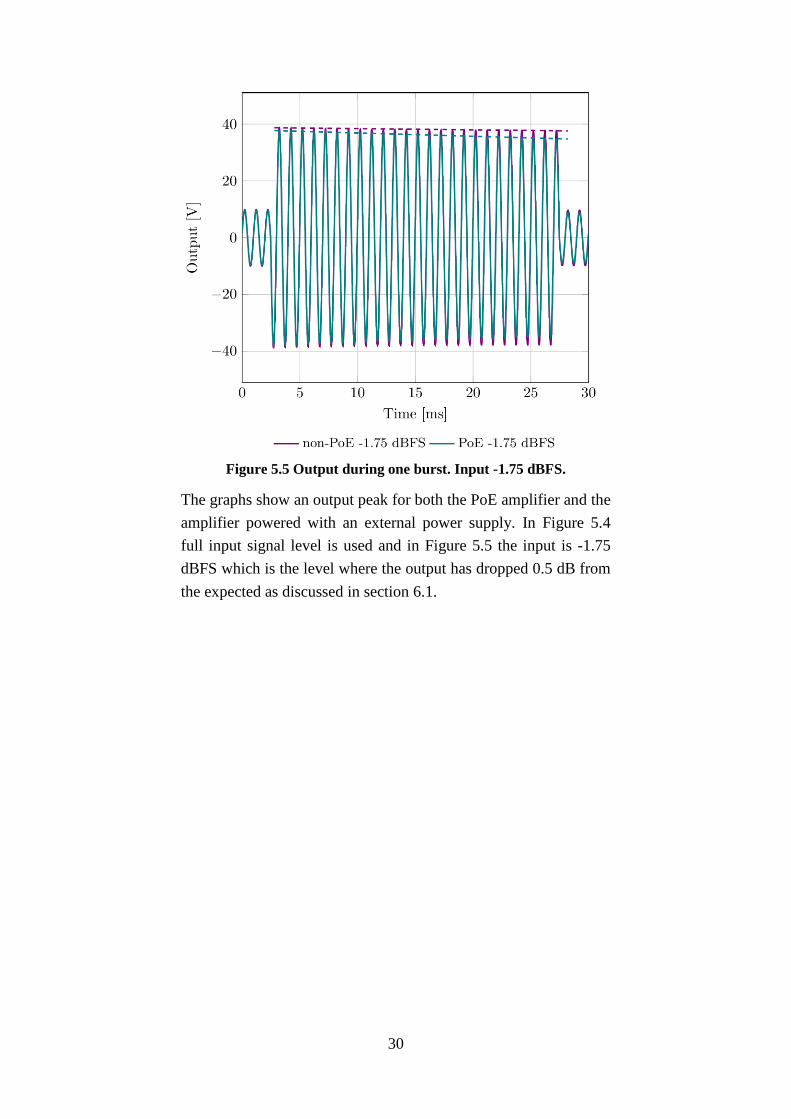
Figure 5.5 Output during one burst. Input -1.75 dBFS.
The graphs show an output peak for both the PoE amplifier and the
amplifier powered with an external power supply. In Figure 5.4
full input signal level is used and in Figure 5.5 the input is -1.75
dBFS which is the level where the output has dropped 0.5 dB from
the expected as discussed in section 6.1.
Page 41
31
5.1.4 Noise floor and THD+N
Figure 5.6 and Figure 5.7 shows a spectrum analysis of the output
from the amplifier when powered by both power methods. The
input signal is a 1 kHz sinusoid wave and the spectra are shown for
-40, -20, -10 and 0 dBFS input level. The magnitude of the output
in the spectra is in dBu.
Figure 5.6 Spectrum analysis for the non-PoE amplifer.
Page 42
32
Figure 5.7 Spectrum analysis for the PoE amplifier.
Page 43
33
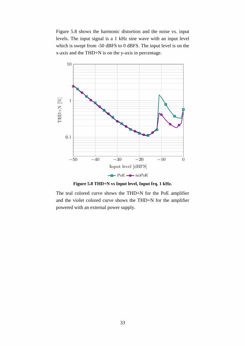
Figure 5.8 shows the harmonic distortion and the noise vs. input
levels. The input signal is a 1 kHz sine wave with an input level
which is swept from -50 dBFS to 0 dBFS. The input level is on the
x-axis and the THD+N is on the y-axis in percentage.
Figure 5.8 THD+N vs Input level, Input frq. 1 kHz.
The teal colored curve shows the THD+N for the PoE amplifier
and the violet colored curve shows the THD+N for the amplifier
powered with an external power supply.
Page 44
34
Figure 5.9 shows the harmonic distortion and the noise vs.
frequency. In this graph the input level is fixed and the frequency
is swept from 20 Hz to 20 kHz. The input level is -15 dBFS which
is a level below the carrier signal artifact discussed in section 6.1.
Input frequency is on the x-axis and THD+N is on the y-axis in
percentage.
Figure 5.9 THD+N vs Input frequency, input level -15dBFS.
The teal colored curve shows the THD+N for the PoE amplifier
and the violet colored curve shows the THD+N for the amplifier
powered by an external power supply.
Page 45
35
6. Discussion
6.1 Discussion of results
With the setup used during the tests the maximum output power is
26.5 W for a continuous signal with 8 Ω load. The input power to
the PD is then 30.9 W. That gives an efficiency of 85.7%.
The results of the linearity measurements show that the amplifier
has good linearity both when it is powered over Ethernet and when
it is powered by an external power supply.
As seen in Figure 5.1, the non-PoE amplifier has good output
power linearity for the whole input range up to around -3 dBFS or
an output of 30 dBu. Above -3 dBFS the output is limited by the
external power supply that is used to power the amplifier. In other
words, it is not the output stage that limits the output power and it
is believed to have a linear output power above -3 dBFS if the
power supply unit would allow it.
The PoE-amplifier has decent output linearity up to an input
of -7 dBFS or an output of 25 dBu which is the point where the
power limit of PoE is reached. But if one looks closely in Figure
5.1, the curve starts to lean away from the ideal curve at an input
of -16 dBFS. This is because at this point the output is 16 dBu
which is driving a load of 8 Ω and it gives an output current just
above 600 mA.
⁄
(6.1)
It means that the current limit of the PoE has been reached and that
the current limiter has started to operate.
Continuous Power
As Figure 5.2 shows the PoE amplifier is able to deliver up to
26.5 W into a load of 8 Ω. At an input of -7 dBFS, which was the
maximum input for good linearity, the continuous output power is
22.6W.
As soon as the input level is higher than -16 dBFS and the current
limiter has started to operate the output is relying on the stored
energy in the capacitor bank. When the average output current is
Page 46
36
higher than the input current of 600 mA the average voltage will
drop in the capacitor bank. And since the output is directly related
to the rail voltage, the output will be affected and that is why the
output power is lower for the PoE amplifier than the non-PoE
amplifier and why the linearity is compromised for higher levels.
Burst Power
In the more music-like situation when playing a “12 dB burst”
signal the PoE amplifier is able to deliver an average of 114 W for
the 25 ms long burst as shown in Figure 5.3. But at this level the
amplitude is dropping quite a lot. At the beginning of the burst the
output power is 131 W but the amplitude is lowered by 11.5%
until the end of the burst as shown in Figure 5.4.
If the amplifier is powered with an external power supply it is able
to deliver an average burst of 133 W (early: 141 W) and during the
burst the amplitude is just dropping 3.2%
The output from the PoE amplifier is 0.67 dB lower than the
output of the non-PoE amplifier given by (6.2) and it is 0.82 dB
lower than the expected output given by (6.3). The expected output
is 138 W.
(6.2)
(6.3)
A more acceptable limitation to the output would be a loss of
0.5 dB from the expected value. At an input of -1.75 dBFS the
output of the PoE amplifier is 81.8 W and it is 0.5 dB below the
expected value.
(6.4)
At this level the amplitude is losing 7.5% throughout the burst as
shown in Figure 5.5.
What can also be noticed is that the first periods of the low part
after the peak also suffer from the depletion of the energy storage
since the output voltage is directly related to the rail voltage. This
happens even if it has a lower output power than the input power
Page 47
37
from PoE and it will be lower than expected until energy storage is
recovered.
THD+N
For lower signals the THD+N is the same for both the PoE and the
non-PoE amplifier as shown in Figure 5.8. The THD+N gets lower
and lower for higher input as expected since the desired signal gets
stronger compared to the noise floor. The THD+N starts to rise for
a signal higher than -17 dBFS and at -11 dBFS, the THD+N level
suddenly jumps quite dramatically.
If observing the output signal with an oscilloscope and zooming in
to time scale 5 µs/div, it is possible to see the traces of the carrier
signal for the PWM that is overlaying the signal. These traces have
a very low level and are outside the hearable range. But at an
output of 8.5 V (input of -11dBFS) there is suddenly a hiccup in
the overlaid trace signal and this artifact is causing the raised
THD+N level. The largest impact from the artifact is when the
output is around 8.5 V because at that time the artifact is on top of
the sine wave. Stronger signals are just passing the troubling level
more quickly.
Not too much effort has been put into explaining exactly what
causes these hiccups, it can either be introduced during the
generation of the PWM signal or it can be introduced by the output
stage. But the phenomena shows up on the amplifier independently
of power supply and it can also be seen on the older prototype that
was the base for this project. What can be observed is that the PoE
amplifier has a harder time dealing with these hiccups.
The spectra for both power supply methods are shown in Figure
5.6 and Figure 5.7 and they are as expected. There are overtones
on all fundamental frequencies and even overtones are higher than
odd. The highest overtone is about 50 dB lower than the desired
signal for both power supply methods and that can be considered
acceptable. It can also be noticed that there is a slightly elevation
of the noise floor for higher frequencies and where there is quite a
dramatic rise of the noise-floor due to the artifact on the carrier
that was explained above.
Page 48
38
6.2 How to use the amplifier
6.2.1 Installation
Permanently audio installations are done in many different places
and for different applications. It can be heavy-duty music
installations at stages and nightclubs or turned down background
music in stores and restaurants. It can also be for reproducing
speech in auditoriums and houses of worship, or announcement
systems and paging systems in malls, stations or other venues.
Many installations are in need of distributing the audio over a large
area or into remote areas of the venue and therefore are in need of
distributed speakers. Distributed speaker systems can be
implemented in many ways and PoE amplifiers can be a good
solution or a good complement in a distributed speaker system.
Distributed speaker system today
If using a traditional low impedance system one can either use
powerful amplifiers that are driving many speakers or one can use
several smaller amplifiers, distributed over the venue, which each
drives a smaller number of speakers. The problem with driving
many speakers from one amplifier is that a complex wiring schema
of parallel and serial speakers must be used to match the desired
impedance of the amplifier. The wires to the speakers cannot be
too long or must be very thick to minimize the losses when driving
high currents. The relative sound pressure for each speaker can just
be controlled by the placement in the parallel / serial network. [12]
[13]
Having many smaller amplifier is more flexible and it can lead to
lower power loses but it comes with a high overhead cost because
every amplifier needs its own power supply unit. It may also imply
that a lot of extra cable installation is needed. In addition to cable
for low level signals and speaker cables, the amplifier must have
wires for power and maybe wires to be controlled.
A smarter way for a distributed speaker system is to, instead of
connecting the speakers in a low impedance system, use a so
called 70-volt or 100-volt system. The amplifiers are designed so
that the full power output exists at 70 V or 100 V RMS. Each
speaker is then connected to the output line with a step-down
transformer that lowers the output voltage to a matching level for
Page 49
39
that speaker. The amplifier sees a high impedance load and one
powerful amplifier can drive many speakers. By having a higher
voltage, less current is needed which gives lesser losses. 70-volt
system is more common in North America while 100-volt systems
are more common in Europe and the rest of the world [13]. From
now on will the text only refer to 100-volt system but all
statements will also apply to 70-volt system if otherwise not stated.
The speakers in a 100-volt system can draw different amount of
power and they can be added and removed without problem as
long as the amplifier is strong enough to drive all speakers. The
sound pressure of each individual speaker can be controlled by
changing the transformer, often done by having many taps on the
transformer which gives different number of turns in the windings.
But it is hard to control during operation and it has only a low
number of fixed levels corresponding to the taps. [12] [13]
Distributed speakers system with PoE
An amplifier that is powered over Ethernet can in many places be
an excellent solution for a distributed speaker system. PoE
amplifiers can cover a large area like a paging system or a sports
arena or it can extend a regular PA system to cover the remote
parts.
The benefit of having PoE amplifiers instead of having many small
amplifiers is that they only needs one single cable to have audio
signal, power and control and every amplifier doesn’t need a
power supply unit to get power from the 230 V power outlets.
One single cable minimizes the need of new wiring. Using
Ethernet has the benefit that no special license is required to be
allowed to install new twisted-pair cables as it is if new power
cords have to be installed. Today many buildings already have an
Ethernet network and since the PoE standard makes sure that non-
PoE devices should not be disturbed by PoE devices, the existing
network can be extended to carry power, audio signals and control
signals to the amplifiers.
Using a well-known standard, as Ethernet is, has the benefit that
many people have the understanding of the system and makes it
easier for the technician to use off-the-shelf products.
Page 50
40
As for the case of 100-volt system, the power in a PoE system is
distributed with higher voltage than a traditional system with low
impedance speakers directly connected to the amplifier and
therefore the losses are less. The sound pressure can be
individually set for different parts of the system like the 100-volt
system but it doesn’t have a limited number of fixed levels and
with Ethernet based control, the sound pressure can be set and
changed without the need of physically walk up to each speaker. A
PoE amplifier also works with all kinds of speakers because it
doesn’t need a transformer.
A PoE system that uses audio over Ethernet would be more
flexible than a 100-volt system in the sense that it would be easy to
route different audio channels to different parts of the system and
it can instantly be reconfigured while in the 100-volt system, all
speakers on the same line must play the same output and has to be
manually reconfigured.
It is also more flexible than the 100-volt system when it comes to
the planning of an installation. In both systems it is easy to add or
remove single speakers gradually. But if the maximum capacity of
the amplifier in the 100-volt system is reached, then it must be
replaced with a more powerful amplifier, and the other way around,
if too much overhead is taken, one might end up with an
unnecessary strong amplifier. The same happens if the maximum
total power of a PoE switch is reached but it is much easier and
cheaper to extend the network with a few extra PoE ports. For
example by add single port PoE injector or a low number PoE
switch.
A 100-volt system has one benefit when it comes to wiring. All the
speakers in a 100-volt system can be decoupled from a long single
cable or they can be branched into many cables. But in the PoE
system, each amplifier must be connected in a star topology where
either the hub is a PSE or each branch has a midspan power
injector.
Self-powered module
A PoE amplifier would work well as a self-powered speaker
module. In other words, a speaker that has a built in power-
amplifier. The small size of the amplifier would make it easy to fit
Page 51
41
into a speaker cabinet and a single cable for both power and audio
signal would make the speaker very easy and flexible to install
since the speaker can be connected anywhere on the network.
6.2.2 Surveillance and emergency system
Today many surveillance system are based on IP and some are
making use of Power over Ethernet. PoE is a good way of
distributing power to units that are placed in inaccessible places
where it can be hard to install many different wires for each unit.
PoE also makes it easy to have a centralized backup power.
Instead of having a UPS backup for each node in a surveillance
system or installing a backup power to the regular AC power grid
in the building; an UPS can be installed at the PSE unit in the PoE
based surveillance system that can provide backup power for the
whole system.
An PoE amplifier would fit nicely in a surveillance system where
there is a need to be able to make announcement calls and voice
alarms.
EN54-16
EN 54 is a standard of the European Union for fire alarms and fire
detection. EN54-16 is a product standard governing "Voice Alarm
Control and Indicating Equipment" (VACIE) which requires,
among other things, that the fire alarm system has a voice alarm
that plays a spoken massage in case of fire. The standard also
requires that the system itself can detect that the path from the
audio source, through the amplifier and to the speaker is intact and
that the system has a redundant power supply.
A system that uses self-powered speakers with power over
Ethernet modules covers many of the requirements of the EN 54
standard. The system can detect that the audio path is intact by
TCP/IP communication from the audio source to the speakers
through the Ethernet cable. The self-powered speaker can be
powered from the regular AC power grid during normal operation
and in case of outage; a centralized UPS can power the speakers
through PoE.
Page 52
42
6.2.3 Centralized Signal Processing and distributed
amplification.
In many audio systems, there is a need for signal processing for
every output node. In high-end amplifiers, signal processing is
built in which makes it possible to e.g. equalize the audio and
compensate for different speakers, add delay and limiters.
Having signal processing in every amplifier in a system is costly
and therefore the signal processing is often centralized and
processed audio is distributed to the output nodes. A PSE with a
DSP matrix that both distributes processed audio and power over
Ethernet to many PoE amplifiers would make a cheap, easy
configured and easy to install system.
A product like Lab.gruppen’s LM26, which is a 2-in / 6-out stand-
alone digital audio loudspeaker processor, merged together with a
24-ports Ethernet switch with PoE would make a unit that has
inputs for analog audio, AES3 and audio over Ethernet and could
send out six different channels of audio to 24 self-powered PoE
speakers.
With TCP/IP communication between the PoE amplifier and the
central unit it would become easy to configure when the amplifier
can identify itself and for example, pre-defined settings can be
loaded in the DSP depending on what Speaker/amplifier that got
connected.
6.3 Future work
The prototype turned out to work pretty well but there are of
course some improvements that can be done.
6.3.1 Feedback loop
This prototype amplifier has no feedback loop. By having a
feedback loop the linearity of the amplifier would increase and it
would mean that the output power would be closer to the expected
output. During a high output signal when the output power starts to
lose its strength due to limited input power, the feedback loop
would increase the gain and the output power would hold its
strength. This requires headroom between the maximum allowed
input signal to the real maximum of the amplifier.
The output power losses comes from the act that the capacitor
bank is losing energy and a feedback loop that increases the gain
Page 53
43
when the stored energy decreases would mean that the energy
decreases even faster. The gain compensation can only be effective
as long as the rail voltage over the capacity bank is higher than the
desired output level. An estimate of the burst output power with a
feedback loop is over 100 W.
One way to close the feedback loop would be for the amplifier to
measure the rail voltage and from that, calculate the gain
compensation it has to add. This is easily done since the output
voltage of a class D amplifier is directly dependent of the rail
voltage.
(6.5)
6.3.2 More power than 25.5 W
The 802.3at standard allows the PSE to provide about 30 W over
two of four pairs in a twisted-pair cable and it gives 25.5 W at the
PD as mentioned in section 2.1.5. But the standard also allows the
PSE to utilize the other two pairs in the cable to provide an
additional 30 W to another PD interface and there is no limitation
how many PD interfaces that can be placed in one unit [4].
In other word, one unit can have two PD interfaces that are
connected to two wire pairs each in in the same cable giving that
twice the power can be distributed to the unit over a single TP-
cable. The guaranteed power at the PD is 51 W and it can be as
high as 68.4 W.
Page 54
44
7. Conclusion
The prototype that is constructed to prove the concept of an
amplifier that is powered over Ethernet was found to work
relatively well. The result shows that PoE has no impact on the
performance or the sound quality for low power levels when the
amplifier is compared to an amplifier with an external power
supply.
The PoE amplifier did meet the proposed goal of 100+ W but not
without losing linearity and having an output that is losing strength
over time throughout a peak. A more reasonable maximum output
power level is found to be 81.8 W which is the level there the
signal only loses 0.5 dB during a peak. With a feedback loop it
would probably be possible to get more than 100 W as output.
A PoE amplifier would be a good solution for a distributed speaker
system. It is not possible to say which of a 100 volt system or a
PoE system that is the best in every situation. It is something that
must be considered case by case. But when it comes to extending
an installation with a small number of speakers or when there is a
need of having different audio channels on each speaker a PoE
system would be perfect.
I think that an amplifier that is powered over Ethernet would be a
great product for the professional audio business. The best section
of application would be as a PoE self-powered speaker. This, since
speakers often are placed where the ability to run many wires is
limited.
Page 55
45
8. References
[1] N. Bouillot, E. Cohen, J. R. Cooperstock,
A. Floros, N. Fonseca, R. Foss, M.
Goodman, J. Grant, K. Gross, S. Harris, B.
Harshbarger, J. Heyraud, L. Jonsson, J.
Narus, M. Page and Snook, "AES White
Paper: Best Practices in Network Audio,"
J. Audio Eng. Soc, vol. 57, no. 9, pp. 729-
741, 2009.
[2] IEEE, Audio/Video Bridging Task Group,
[Online]. Available:
http://ieee802.org/1/pages/avbridges.html.
[3] IEEE Std 802.3af-2003, IEEE Standard for
Information Technology -
Telecommunications and Information
Exchange Between Systems - Local and
Metropolitan Area Networks - Specific
Requirements - Part 3: Carrier Sense
Multiple Access with Collision Detection
(CSMA/CD) Access Method, 2003.
[4] IEEE Std 803.2at-2009, IEEE Standard for
Information technology -
Telecommunications and information
exchange between systems - Local and
metropolitan area networks - Specific
requirements Part 3: Carrier Sense Multiple
Access with Collision Detection
(CSMA/CD) Access Method an, 2009.
[5] D. Self, Audio power amplifier design
handbook, 5th ed., Oxford: Focal Press,
2009.
[6] Alliance for Telecommunications Industry
Page 56
46
Solutions, ANSI T1.523-2011, 2011.
[7] R. C. Cabot, "Fundamentals of Modern
Audio Measurement," Jurnal of the Audio
Engineering Society, vol. 47, no. 9, pp.
738-744, 746-762, September 1999.
[8] E. Gaalaas, "Class D Audio Amplifiers:
What, Why, and How," Analog Dialogue,
vol. 40, no. 2, pp. 6-12, 2006.
[9] Linear Technology, Datasheet: LTC4265 -
IEEE 802.3at High Power PD Interface
Controller with 2-Event Classification
Recognition, Milpitas: Linear Technology,
2009.
[10] STMicroelectronics, Datasheet: STA516B -
65-volt, 7.5-amp, quad power half bridge,
STMicroelectronics, 2010.
[11] Silicon Laboratories Inc., Single-port IEEE
802.3at PoE/PoE+ PSE Interface, Austin:
Silicon Laboratories, 2009.
[12] J. Eargle, Sound System Design Reference
Manual, Northridge: JBL Professional,
1999.
[13] R. Kamiet, "Distributed speaker systems
101," Sound & Video Contractor, vol. 19,
no. 2, pp. 70-72, 2001.