9
Audio DAC Matt Smith Alfred Wanga CSE598A/EE597G Analog-Digital Mixed-Signal CMOS Chip Design Spring 2006
| Date post: | 14-Dec-2015 |
| Category: |
Documents |
| Upload: | ashlynn-richardson |
| View: | 216 times |
| Download: | 0 times |

Audio DACMatt Smith
Alfred Wanga
CSE598A/EE597G
Analog-Digital Mixed-Signal CMOS Chip Design
Spring 2006
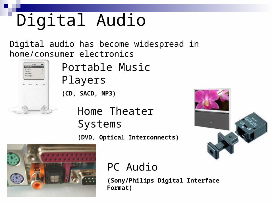
Digital audio has become widespread in home/consumer electronics
Portable Music Players(CD, SACD, MP3)
PC Audio(Sony/Philips Digital Interface Format)
Home Theater Systems(DVD, Optical Interconnects)
Digital Audio
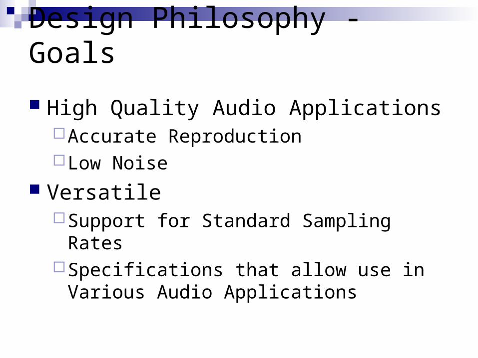
Design Philosophy - Goals
High Quality Audio ApplicationsAccurate ReproductionLow Noise
VersatileSupport for Standard Sampling RatesSpecifications that allow use in Various Audio
Applications

Figures of Merit
Sampling Rate Support common sampling speeds (96kHz)
Bit Depth Finer Resolution → Better fidelity (>= 16bit)
Total Harmonic Distortion + Noise (THD+N) Important for audio applications (< 1% THD+N)
Signal to Noise Ratio (SNR) Equal or better than digital source (>= 100dB)
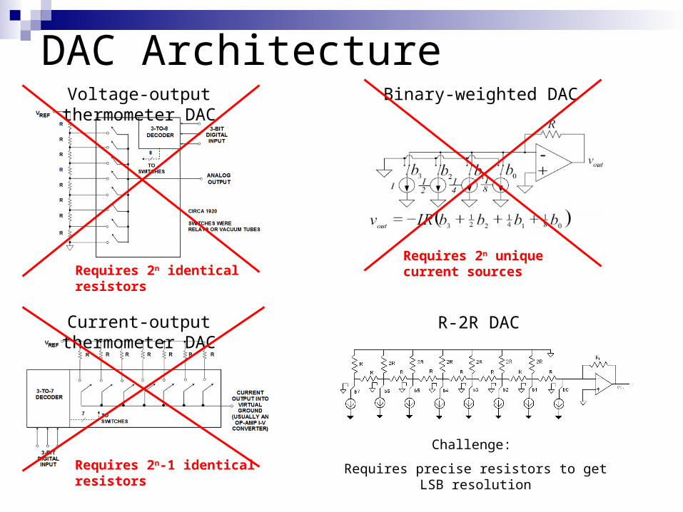
Voltage-output thermometer DAC
Current-output thermometer DAC
Binary-weighted DAC
R-2R DAC
Requires 2n identical resistors
Requires 2n-1 identical resistors
Requires 2n unique current sources
Challenge:
Requires precise resistors to get LSB resolution
DAC Architecture
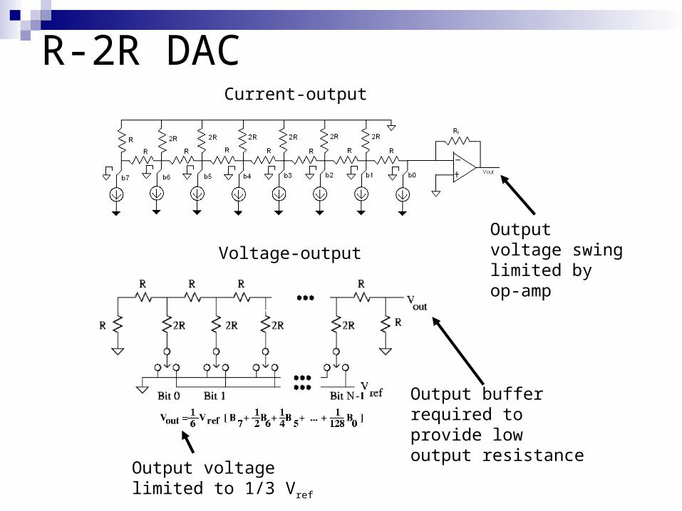
Current-output
Voltage-output
Output buffer required to provide low output resistance
Output voltage swing limited by op-amp
Output voltage limited to 1/3 Vref
R-2R DAC
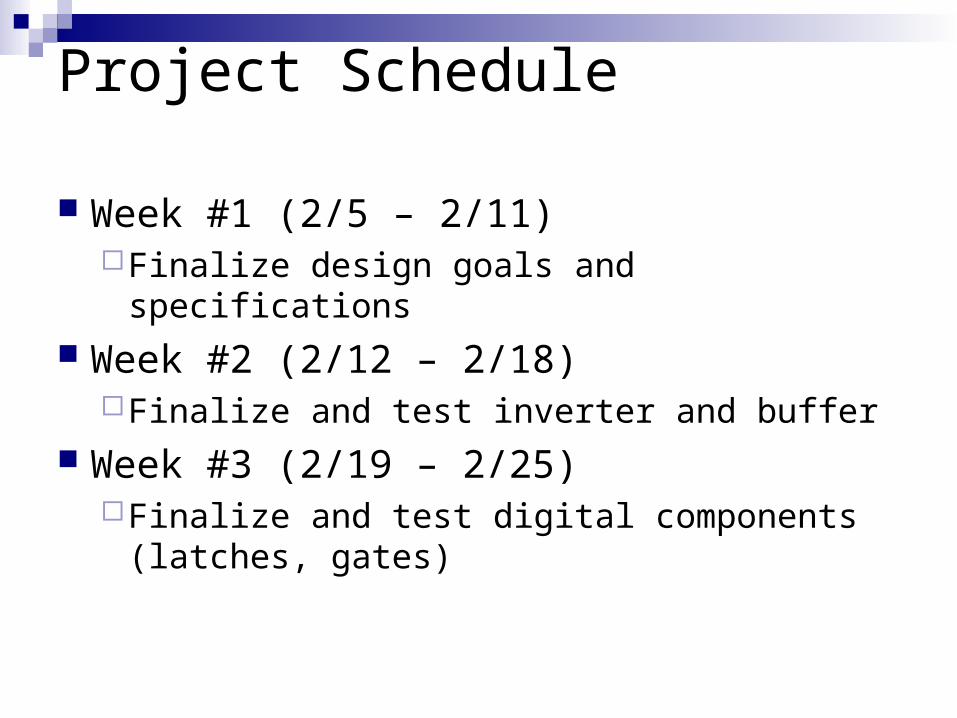
Project Schedule
Week #1 (2/5 – 2/11)Finalize design goals and specifications
Week #2 (2/12 – 2/18)Finalize and test inverter and buffer
Week #3 (2/19 – 2/25)Finalize and test digital components (latches,
gates)

Project Schedule
Week #4 (2/26 – 3/4)Begin operational amplifier design
Week #5 (3/5 – 3/11)Finalize design for operational amplifier
Week #6 (3/12 – 3/18)Finalize resistor designProject Progress Report

Project Schedule
Week #7 (3/19 – 3/25)Finalize and test voltage reference circuitry
Week #8 (3/26 – 4/1)Complete final circuit design and layout
Week #9 (4/2 – 4/8)Complete circuit layout and testing
Week #10 (4/9 – 4/13)Final Project Presentation


