Users Guide August 2011 Revision 0.4 – preliminary Page 1 of 31 Texas Instruments Dual EVM BoC Card - Quick Start Guide High Density Multiprocessor DSP’s Abstract This document is provided as a quick start guide for using the Texas Instruments BoC (Break out Card). The breakout card is intended to provide communication support between Texas Instruments EVM’s which contain an AMC B+ interface. The EVM BoC is intended to support EVM to EVM communication for SRIO, PCIe, SGMII, and AIF. Table of Contents Abstract ........................................................................................................................................................................... 1 Table of Contents ........................................................................................................................................................... 1 Table of Figures.............................................................................................................................................................. 2 Table of Tables ............................................................................................................................................................... 2 I. OVERVIEW ........................................................................................................................................................... 3 I. Introduction ...................................................................................................................................................... 3 II. Hardware Description...................................................................................................................................... 3 II. Hardware Configuration ....................................................................................................................................... 6 I. Initial Installation Procedure ........................................................................................................................... 6 II. Default Jumper and Pin Settings ...................................................................................................................... 6 III. BoC Logic Power Source Selection [20].......................................................................................................... 6 IV. EVM Power Source [16, 17, 18] ...................................................................................................................... 7 V. Emulation Interface [1] .................................................................................................................................... 8 VI. SGMII Interface ............................................................................................................................................... 8 VII. PCIE Interface ................................................................................................................................................. 8 VIII. SRIO (Serial RapidIO) Interface ...................................................................................................................... 9 IX. AIF (Antenna Interface) Interface .................................................................................................................... 9 X. I2C interface [5, 9, 11, 23]............................................................................................................................... 9 XI. Common REFCLK Source ............................................................................................................................. 10 a. REFCLK Oscillator Enable Header [19]....................................................................................................... 10 b. REFCLK Signal Levels................................................................................................................................... 10 XII. Timer0 Output Headers [12, 22] .................................................................................................................... 12 XIII. Timer0 Input Header [10, 24] ........................................................................................................................ 12 XIV. Common RP1CLK Source .............................................................................................................................. 12 a. RP1CLK Oscillator Enable Header [8] ......................................................................................................... 12 b. RP1CLK Signal Levels ................................................................................................................................... 13 c. Alternate RP1CLK Inputs [15]....................................................................................................................... 14 XV. Common TCLK_B Source .............................................................................................................................. 14 a. TCLK_B Oscillator Enable Header [14] ....................................................................................................... 14 b. TCLK_B Signal Outputs [2, 13] ..................................................................................................................... 15 c. TCLK_A Signal Outputs [2, 13] ..................................................................................................................... 16 XVI. Common PCIeREFCLK Source [25] ............................................................................................................. 17
Abstract This document is provided as a quick start guide for using the Texas Instruments BoC (Break out Card). The breakout card is intended to provide communication support between Texas Instruments EVM’s which contain an AMC B+ interface. The EVM BoC is intended to support EVM to EVM communication for SRIO, PCIe, SGMII, and AIF.
Table of Contents Abstract ........................................................................................................................................................................... 1
Table of Contents ........................................................................................................................................................... 1
Table of Figures .............................................................................................................................................................. 2
Table of Tables ............................................................................................................................................................... 2
I. OVERVIEW ........................................................................................................................................................... 3
I. Introduction ...................................................................................................................................................... 3 II. Hardware Description...................................................................................................................................... 3
II. Hardware Configuration ....................................................................................................................................... 6
I. Initial Installation Procedure ........................................................................................................................... 6 II. Default Jumper and Pin Settings ...................................................................................................................... 6 III. BoC Logic Power Source Selection [20].......................................................................................................... 6 IV. EVM Power Source [16, 17, 18] ...................................................................................................................... 7 V. Emulation Interface [1] .................................................................................................................................... 8 VI. SGMII Interface ............................................................................................................................................... 8 VII. PCIE Interface ................................................................................................................................................. 8 VIII. SRIO (Serial RapidIO) Interface ...................................................................................................................... 9 IX. AIF (Antenna Interface) Interface .................................................................................................................... 9 X. I2C interface [5, 9, 11, 23] ............................................................................................................................... 9 XI. Common REFCLK Source ............................................................................................................................. 10 a. REFCLK Oscillator Enable Header [19]....................................................................................................... 10 b. REFCLK Signal Levels................................................................................................................................... 10 XII. Timer0 Output Headers [12, 22] .................................................................................................................... 12 XIII. Timer0 Input Header [10, 24] ........................................................................................................................ 12 XIV. Common RP1CLK Source .............................................................................................................................. 12 a. RP1CLK Oscillator Enable Header [8] ......................................................................................................... 12 b. RP1CLK Signal Levels ................................................................................................................................... 13 c. Alternate RP1CLK Inputs [15]....................................................................................................................... 14 XV. Common TCLK_B Source .............................................................................................................................. 14 a. TCLK_B Oscillator Enable Header [14] ....................................................................................................... 14 b. TCLK_B Signal Outputs [2, 13] ..................................................................................................................... 15 c. TCLK_A Signal Outputs [2, 13] ..................................................................................................................... 16 XVI. Common PCIeREFCLK Source [25] ............................................................................................................. 17
5
5
4
4
3
3
2
2
1
1
D D
C C
B B
A A
Board ASGMII [1]
TDO Output from Brd A to Brd B
Board AJTAG Interface
Board AClocks
Board ASGMII [0]
Board ARP1CLK
Board AAIF[0:5]
Board AAIF CLK & FS
Board AExpansion I2C
Board ASRIO[1:4]
Board APCIe[4:7]
FROM EVM A
TO EVM A
FROM EVM A
TO EVM A
FROM EVM A
TO EVM A
FROM EVM A
TO EVM A
FROM EVM A
TO EVM A
FROM EVM A
TO EVM A
FROM EVM A
TO EVM A
FROM EVM A
TO EVM A
FROM EVM A
TO EVM A
FROM EVM A
TO EVM A
FROM EVM A
TO EVM A
FROM EVM A
TO EVM A
FROM EVM A
TO EVM A
FROM EVM A
TO EVM A
FROM EVM A
TO EVM A
FROM EVM A
TO EVM A
TO EVM A
TO EVM A
TO EVM A
TO EVM A
CONNECTOR REFLECTS BACKPLANE PIN OUTS
TDITDO_2_TDITRST#TMSTCK
A_AMC0_SGMII1_TX_DPA_AMC0_SGMII1_TX_DN
A_AMC0_SGMII1_RX_DPA_AMC0_SGMII1_RX_DN
A_DSP_RP1CLKNA_DSP_RP1CLKP
A_AMCC_P7_PCIe_RX2PA_AMCC_P7_PCIe_RX2N
A_AMCC_P6_PCIe_RX1PA_AMCC_P6_PCIe_RX1N
A_AMCC_P7_PCIe_TX2PA_AMCC_P7_PCIe_TX2N
A_AMCC_P6_PCIe_TX1PA_AMCC_P6_PCIe_TX1N
A_AMCC_P13_AIF1_RXNA_AMCC_P13_AIF1_RXP
A_AMCC_P13_AIF1_TXPA_AMCC_P13_AIF1_TXN
A_AMCC_P14_AIF2_RXPA_AMCC_P14_AIF2_RXN
A_AMCC_P14_AIF2_TXPA_AMCC_P14_AIF2_TXN
A_AMCC_P15_AIF3_RXPA_AMCC_P15_AIF3_RXN
A_AMCC_P15_AIF3_TXPA_AMCC_P15_AIF3_TXN
A_AMCC_P12_AIF0_RXNA_AMCC_P12_AIF0_RXP
A_AMCC_P12_AIF0_TXPA_AMCC_P12_AIF0_TXN
A_AMCC_P17_AIF4_RXPA_AMCC_P17_AIF4_RXN
A_AMCC_P17_AIF4_TXPA_AMCC_P17_AIF4_TXN
A_AMCC_P18_AIF5_RXPA_AMCC_P18_AIF5_RXN
A_AMCC_P18_AIF5_TXPA_AMCC_P18_AIF5_TXN
A_AMC0_SGMII0_TX_DPA_AMC0_SGMII0_TX_DN
A_AMCC_P11_SRIO4_RXNA_AMCC_P11_SRIO4_RXP
A_AMCC_P9_SRIO2_TXNA_AMCC_P9_SRIO2_TXP
A_AMCC_P10_SRIO3_RXPA_AMCC_P10_SRIO3_RXN
A_AMCC_P8_SRIO1_TXNA_AMCC_P8_SRIO1_TXP
A_AMCC_P9_SRIO2_RXPA_AMCC_P9_SRIO2_RXN
A_AMCC_P11_SRIO4_TXPA_AMCC_P11_SRIO4_TXN
A_AMCC_P8_SRIO1_RXPA_AMCC_P8_SRIO1_RXN
A_AMCC_P10_SRIO3_TXPA_AMCC_P10_SRIO3_TXN
A_PCIE_REF_CLK_P
A_AMC0_SGMII0_RX_DPA_AMC0_SGMII0_RX_DN
A_PCIE_REF_CLK_N
A_AMCC_P5_PCIe_RX2PA_AMCC_P5_PCIe_RX2N
A_AMCC_P4_PCIe_RX1PA_AMCC_P4_PCIe_RX1N
A_AMCC_P5_PCIe_TX2PA_AMCC_P5_PCIe_TX2N
A_AMCC_P4_PCIe_TX1PA_AMCC_P4_PCIe_TX1N
A_TCLKA_PA_TCLKA_N
A_TCLKB_PA_TCLKB_N
A_REFCLK_PA_REFCLK_N
A_TIMEROUT_0A_TIMERIN_0
A_RP1FBPA_RP1FBN
A_DSP_SDA_AMCA_DSP_SCL_AMC
A_PHYSYNCA_RADSYNC
A_VCC12
INB_AMC0_SGMII1_TX_DP4INB_AMC0_SGMII1_TX_DN4
OUTA_AMC0_SGMII1_TX_DP4OUTA_AMC0_SGMII1_TX_DN4
IN TDI 7OUT TDO_2_TDI 4
IN TRST# 4,7IN TMS 4,7IN A_TCK 7
IN A_DSP_RP1CLKN 5IN A_DSP_RP1CLKP 5
OUTA_AMCC_P6_PCIe_TX1P4OUTA_AMCC_P6_PCIe_TX1N4
INB_AMCC_P6_PCIe_TX1P4INB_AMCC_P6_PCIe_TX1N4
INB_AMCC_P7_PCIe_TX2P4INB_AMCC_P7_PCIe_TX2N4
OUTA_AMCC_P7_PCIe_TX2P4OUTA_AMCC_P7_PCIe_TX2N4
INB_AMC0_SGMII0_TX_DP4INB_AMC0_SGMII0_TX_DN4
OUTA_AMC0_SGMII0_TX_DP4OUTA_AMC0_SGMII0_TX_DN4
OUTA_AMCC_P4_PCIe_TX1P4OUTA_AMCC_P4_PCIe_TX1N4
INB_AMCC_P4_PCIe_TX1P4INB_AMCC_P4_PCIe_TX1N4
INB_AMCC_P5_PCIe_TX2P4INB_AMCC_P5_PCIe_TX2N4
OUTA_AMCC_P5_PCIe_TX2P4OUTA_AMCC_P5_PCIe_TX2N4
INA_TCLKA_P5INA_TCLKA_N5
INA_TCLKB_P5INA_TCLKB_N5
INA_PCIE_REF_CLK_P5INA_PCIE_REF_CLK_N5
IN A_RP1FBN 6IN A_RP1FBP 6
IN A_RADSYNC 6IN A_PHYSYNC 6
IN B_AMCC_P18_AIF5_TXN 4IN B_AMCC_P18_AIF5_TXP 4
OUT A_AMCC_P17_AIF4_TXP 4OUT A_AMCC_P17_AIF4_TXN 4
IN B_AMCC_P17_AIF4_TXN 4IN B_AMCC_P17_AIF4_TXP 4
OUT A_AMCC_P18_AIF5_TXP 4OUT A_AMCC_P18_AIF5_TXN 4
OUT A_AMCC_P15_AIF3_TXP 4OUT A_AMCC_P15_AIF3_TXN 4
OUT A_AMCC_P14_AIF2_TXP 4OUT A_AMCC_P14_AIF2_TXN 4
IN B_AMCC_P15_AIF3_TXN 4IN B_AMCC_P15_AIF3_TXP 4
OUT A_AMCC_P13_AIF1_TXP 4OUT A_AMCC_P13_AIF1_TXN 4
IN B_AMCC_P14_AIF2_TXN 4IN B_AMCC_P14_AIF2_TXP 4
OUT A_AMCC_P12_AIF0_TXP 4OUT A_AMCC_P12_AIF0_TXN 4
IN B_AMCC_P13_AIF1_TXN 4IN B_AMCC_P13_AIF1_TXP 4
IN B_AMCC_P12_AIF0_TXN 4IN B_AMCC_P12_AIF0_TXP 4
OUT A_AMCC_P11_SRIO4_TXP 4OUT A_AMCC_P11_SRIO4_TXN 4
IN B_AMCC_P11_SRIO4_TXP 4IN B_AMCC_P11_SRIO4_TXN 4
OUT A_AMCC_P10_SRIO3_TXP 4OUT A_AMCC_P10_SRIO3_TXN 4
IN B_AMCC_P10_SRIO3_TXP 4IN B_AMCC_P10_SRIO3_TXN 4
OUT A_AMCC_P9_SRIO2_TXP 4OUT A_AMCC_P9_SRIO2_TXN 4
IN B_AMCC_P9_SRIO2_TXP 4IN B_AMCC_P9_SRIO2_TXN 4
OUT A_AMCC_P8_SRIO1_TXP 4OUT A_AMCC_P8_SRIO1_TXN 4
IN B_AMCC_P8_SRIO1_TXP 4IN B_AMCC_P8_SRIO1_TXN 4
BI A_AMC_EXP_SDA 6
OUT A_TIMERIN_0 6
IN A_AMC_EXP_SCL 6
IN A_TIMEROUT_0 6
IN A_REFCLK_N 7IN A_REFCLK_P 7
Title
Size Document Number Rev
Date: Sheet of
<Doc> E
LC_2-EVM_BoC-0002 - Board B Interface
B
3 10Friday, September 09, 2011
Title
Size Document Number Rev
Date: Sheet of
<Doc> E
LC_2-EVM_BoC-0002 - Board B Interface
B
3 10Friday, September 09, 2011
Title
Size Document Number Rev
Date: Sheet of
<Doc> E
LC_2-EVM_BoC-0002 - Board B Interface
B
3 10Friday, September 09, 2011
R3 DNIR4 DNI
R50R60
A1
AMC_BACKPLANE_CONNECTOR<Characteristic>
GND_11
GND_27
GND_310
PWR_12V_12
PS13
MP4
GA05
RSRVD66
RSRVD88
PWR_12V_29
Rx0+11
Rx0-12
GND_413
Tx0+14
Tx0-15
GND_516
GA117
PWR_12V_318
GND_619
Rx1+20
Rx1-21
GND_722
Tx1+23
Tx1-24
GND_825
GA226
PWR_12V_427
GND_928
Rx2+29
Rx2-30
GND_1031
Tx2+32
Tx2-33
GND_1134
Rx3+35
Rx3-36
GND_1237
Tx3+38
Tx3-39
GND_1340
ENABLE41
PWR_12V_542
GND_1443
Rx4+44
Rx4-45
GND_1546
Tx4+47
Tx4-48
GND_1649
Rx5+50
Rx5-51
GND_1752
Tx5+53
Tx5-54
GND_1855
SCL_L56
GND_1958
Rx6+59
Rx6-60
GND_2061
Tx6+62
Tx6-63
GND_2164
Rx7+65
Rx7-66
GND_2267
Tx7+68
Tx7-69
GND_2370
SDA_L71
PWR_12V_657
PWR_12V_772
GND_2473
TCLKA+74
TCLKA-75
GND_2576
TCLKB+77
TCLKB-78
GND_2679
FCLKA+80
FCLKA-81
GND_2782
PS083
PWR_12V_884
GND_2885
GND_2986Tx8-87Tx8+88
Rx8+91
Rx8-90
GND_3089
Tx9+94
Tx9-93
GND_3192
Rx9+97
Rx9-96
GND_3295
Tx10+100
Tx10-99
GND_3398
Rx10+103
Rx10-102
GND_34101
Tx11+106
Tx11-105
GND_35104
Rx11+109
Rx11-108
GND_36107
Tx12+112
Tx12-111
GND_37110
Rx12+115
Rx12-114
GND_38113
Tx13+118
Tx13-117
GND_39116
Rx13+121
Rx13-120
GND_40119
Tx14+124
Tx14-123
GND_41122
Rx14+127
Rx14-126
GND_42125
GND_43128
Tx15+130
Tx15-129
GND_44131Rx15-132Rx15+133GND_45134
TCLKC+136
TCLKC-135
TCLKD+139
TCLKD-138
GND_46137
Tx17+142
Tx17-141
GND_47140
Rx17+145
Rx17-144
GND_48143
Rx18+151
Rx18-150
GND_50149
Tx18+148
Tx18-147
GND_49146
Rx19+157
Rx19-156
GND_52155
Tx19+154
Tx19-153
GND_51152
Rx20+163
Rx20-162
GND_54161
Tx20+160
Tx20-159
GND_53158
GND_55164TCK165TMS166TRST167TDO168TDI169GND_56170
R10R20
5
5
4
4
3
3
2
2
1
1
D D
C C
B B
A A
Board BSGMII [1]
TDO Output from Brd A, TDI Input to Brd B
Board BJTAG Interface
Board BClocks
Board BSGMII [0]
Board BPCIe[4:7]
Board BRP1CLK
Board BAIF[0:5]
Board BAIF CLK & FS
Board BExpansion I2C
Board BSRIO[1:4]
TO EVM B
FROM EVM B
TO EVM B
FROM EVM B
TO EVM B
FROM EVM B
TO EVM B
FROM EVM B
TO EVM B
FROM EVM B
TO EVM B
FROM EVM B
TO EVM B
FROM EVM B
TO EVM B
FROM EVM B
TO EVM B
FROM EVM B
TO EVM B
FROM EVM B
TO EVM B
FROM EVM B
TO EVM B
FROM EVM B
TO EVM B
FROM EVM B
TO EVM B
FROM EVM B
TO EVM B
FROM EVM B
TO EVM B
FROM EVM B
TO EVM B
TO EVM B
TO EVM B
TO EVM B
TDO_2_TDITDOTRST#TMSTCK
B_AMC0_SGMII1_TX_DPB_AMC0_SGMII1_TX_DN
B_AMC0_SGMII1_RX_DPB_AMC0_SGMII1_RX_DN
B_AMC0_SGMII0_RX_DPB_AMC0_SGMII0_RX_DN
B_AMCC_P7_PCIe_RX2PB_AMCC_P7_PCIe_RX2N
B_AMCC_P6_PCIe_RX1PB_AMCC_P6_PCIe_RX1N
B_AMCC_P7_PCIe_TX2PB_AMCC_P7_PCIe_TX2N
B_AMCC_P6_PCIe_TX1PB_AMCC_P6_PCIe_TX1N
B_DSP_RP1CLKNB_DSP_RP1CLKP
B_AMCC_P13_AIF1_RXNB_AMCC_P13_AIF1_RXP
B_AMCC_P13_AIF1_TXPB_AMCC_P13_AIF1_TXN
B_AMCC_P14_AIF2_RXPB_AMCC_P14_AIF2_RXN
B_AMCC_P14_AIF2_TXPB_AMCC_P14_AIF2_TXN
B_AMCC_P15_AIF3_RXPB_AMCC_P15_AIF3_RXN
B_AMCC_P15_AIF3_TXPB_AMCC_P15_AIF3_TXN
B_AMCC_P12_AIF0_RXNB_AMCC_P12_AIF0_RXP
B_AMCC_P12_AIF0_TXPB_AMCC_P12_AIF0_TXN
B_AMCC_P17_AIF4_RXPB_AMCC_P17_AIF4_RXN
B_AMCC_P17_AIF4_TXPB_AMCC_P17_AIF4_TXN
B_AMCC_P18_AIF5_RXPB_AMCC_P18_AIF5_RXN
B_AMCC_P18_AIF5_TXPB_AMCC_P18_AIF5_TXN
B_AMC0_SGMII0_TX_DPB_AMC0_SGMII0_TX_DN
B_AMCC_P11_SRIO4_RXNB_AMCC_P11_SRIO4_RXP
B_AMCC_P9_SRIO2_TXNB_AMCC_P9_SRIO2_TXP
B_AMCC_P10_SRIO3_RXPB_AMCC_P10_SRIO3_RXN
B_AMCC_P8_SRIO1_TXNB_AMCC_P8_SRIO1_TXP
B_AMCC_P9_SRIO2_RXPB_AMCC_P9_SRIO2_RXN
B_AMCC_P11_SRIO4_TXPB_AMCC_P11_SRIO4_TXN
B_AMCC_P8_SRIO1_RXPB_AMCC_P8_SRIO1_RXN
B_AMCC_P10_SRIO3_TXPB_AMCC_P10_SRIO3_TXN
B_PCIE_REF_CLK_PB_PCIE_REF_CLK_N
B_AMCC_P5_PCIe_RX2PB_AMCC_P5_PCIe_RX2N
B_AMCC_P4_PCIe_RX1PB_AMCC_P4_PCIe_RX1N
B_AMCC_P5_PCIe_TX2PB_AMCC_P5_PCIe_TX2N
B_AMCC_P4_PCIe_TX1PB_AMCC_P4_PCIe_TX1N
B_TCLKA_PB_TCLKA_N
B_TCLKB_PB_TCLKB_N
B_REFCLK_PB_REFCLK_N
B_TIMEROUT_0B_TIMERIN_0
B_RP1FBPB_RP1FBN
B_EXP_SDAB_EXP_SCL
B_PHYSYNCB_RADSYNC
B_VCC12
INA_AMC0_SGMII1_TX_DP3INA_AMC0_SGMII1_TX_DN3
OUTB_AMC0_SGMII1_TX_DP3
IN TDO_2_TDI 3
OUTB_AMC0_SGMII1_TX_DN3
OUT TDO 7IN TRST# 3,7IN TMS 3,7IN B_TCK 7
OUTB_AMCC_P6_PCIe_TX1P3OUTB_AMCC_P6_PCIe_TX1N3
OUTB_AMCC_P7_PCIe_TX2P3OUTB_AMCC_P7_PCIe_TX2N3
INA_AMCC_P7_PCIe_TX2P3INA_AMCC_P7_PCIe_TX2N3
INA_AMCC_P6_PCIe_TX1P3INA_AMCC_P6_PCIe_TX1N3
IN B_DSP_RP1CLKN 5IN B_DSP_RP1CLKP 5
BI B_AMC_EXP_SDA 6IN B_AMC_EXP_SCL 6
OUT B_TIMERIN_0 6IN B_TIMEROUT_0 6
IN B_REFCLK_N 7IN B_REFCLK_P 7
INA_AMC0_SGMII0_TX_DP3INA_AMC0_SGMII0_TX_DN3
OUTB_AMC0_SGMII0_TX_DP3OUTB_AMC0_SGMII0_TX_DN3
OUTB_AMCC_P4_PCIe_TX1P3OUTB_AMCC_P4_PCIe_TX1N3
OUTB_AMCC_P5_PCIe_TX2P3OUTB_AMCC_P5_PCIe_TX2N3
INA_AMCC_P5_PCIe_TX2P3INA_AMCC_P5_PCIe_TX2N3
INA_AMCC_P4_PCIe_TX1P3INA_AMCC_P4_PCIe_TX1N3
INB_PCIE_REF_CLK_P5INB_PCIE_REF_CLK_N5
INB_TCLKA_P5INB_TCLKA_N5
INB_TCLKB_P5INB_TCLKB_N5
IN B_RP1FBN 6IN B_RP1FBP 6
IN B_RADSYNC 6IN B_PHYSYNC 6
IN A_AMCC_P18_AIF5_TXN 3IN A_AMCC_P18_AIF5_TXP 3
IN A_AMCC_P17_AIF4_TXP 3IN A_AMCC_P17_AIF4_TXN 3
OUT B_AMCC_P17_AIF4_TXP 3OUT B_AMCC_P17_AIF4_TXN 3
OUT B_AMCC_P18_AIF5_TXP 3OUT B_AMCC_P18_AIF5_TXN 3
IN A_AMCC_P14_AIF2_TXP 3IN A_AMCC_P14_AIF2_TXN 3
OUT B_AMCC_P14_AIF2_TXP 3OUT B_AMCC_P14_AIF2_TXN 3
IN A_AMCC_P15_AIF3_TXN 3IN A_AMCC_P15_AIF3_TXP 3
OUT B_AMCC_P15_AIF3_TXP 3OUT B_AMCC_P15_AIF3_TXN 3
IN A_AMCC_P12_AIF0_TXP 3IN A_AMCC_P12_AIF0_TXN 3
OUT B_AMCC_P12_AIF0_TXP 3OUT B_AMCC_P12_AIF0_TXN 3
IN A_AMCC_P13_AIF1_TXN 3IN A_AMCC_P13_AIF1_TXP 3
OUT B_AMCC_P13_AIF1_TXP 3OUT B_AMCC_P13_AIF1_TXN 3
OUT B_AMCC_P11_SRIO4_TXP 3OUT B_AMCC_P11_SRIO4_TXN 3
IN A_AMCC_P11_SRIO4_TXP 3IN A_AMCC_P11_SRIO4_TXN 3
OUT B_AMCC_P10_SRIO3_TXP 3OUT B_AMCC_P10_SRIO3_TXN 3
IN A_AMCC_P10_SRIO3_TXP 3IN A_AMCC_P10_SRIO3_TXN 3
OUT B_AMCC_P9_SRIO2_TXP 3OUT B_AMCC_P9_SRIO2_TXN 3
IN A_AMCC_P9_SRIO2_TXP 3IN A_AMCC_P9_SRIO2_TXN 3
OUT B_AMCC_P8_SRIO1_TXP 3OUT B_AMCC_P8_SRIO1_TXN 3
IN A_AMCC_P8_SRIO1_TXP 3IN A_AMCC_P8_SRIO1_TXN 3
Title
Size Document Number Rev
Date: Sheet of
<Doc> E
LC_2-EVM_BoC-0002 - Board B Interface
B
4 10Friday, September 09, 2011
Title
Size Document Number Rev
Date: Sheet of
<Doc> E
LC_2-EVM_BoC-0002 - Board B Interface
B
4 10Friday, September 09, 2011
Title
Size Document Number Rev
Date: Sheet of
<Doc> E
LC_2-EVM_BoC-0002 - Board B Interface
B
4 10Friday, September 09, 2011
R110R120
R70
R8 DNIR9
0
B1
AMC_BACKPLANE_CONNECTOR<Characteristic>
GND_11
GND_27
GND_310
PWR_12V_12
PS13
MP4
GA05
RSRVD66
RSRVD88
PWR_12V_29
Rx0+11
Rx0-12
GND_413
Tx0+14
Tx0-15
GND_516
GA117
PWR_12V_318
GND_619
Rx1+20
Rx1-21
GND_722
Tx1+23
Tx1-24
GND_825
GA226
PWR_12V_427
GND_928
Rx2+29
Rx2-30
GND_1031
Tx2+32
Tx2-33
GND_1134
Rx3+35
Rx3-36
GND_1237
Tx3+38
Tx3-39
GND_1340
ENABLE41
PWR_12V_542
GND_1443
Rx4+44
Rx4-45
GND_1546
Tx4+47
Tx4-48
GND_1649
Rx5+50
Rx5-51
GND_1752
Tx5+53
Tx5-54
GND_1855
SCL_L56
GND_1958
Rx6+59
Rx6-60
GND_2061
Tx6+62
Tx6-63
GND_2164
Rx7+65
Rx7-66
GND_2267
Tx7+68
Tx7-69
GND_2370
SDA_L71
PWR_12V_657
PWR_12V_772
GND_2473
TCLKA+74
TCLKA-75
GND_2576
TCLKB+77
TCLKB-78
GND_2679
FCLKA+80
FCLKA-81
GND_2782
PS083
PWR_12V_884
GND_2885
GND_2986Tx8-87Tx8+88
Rx8+91
Rx8-90
GND_3089
Tx9+94
Tx9-93
GND_3192
Rx9+97
Rx9-96
GND_3295
Tx10+100
Tx10-99
GND_3398
Rx10+103
Rx10-102
GND_34101
Tx11+106
Tx11-105
GND_35104
Rx11+109
Rx11-108
GND_36107
Tx12+112
Tx12-111
GND_37110
Rx12+115
Rx12-114
GND_38113
Tx13+118
Tx13-117
GND_39116
Rx13+121
Rx13-120
GND_40119
Tx14+124
Tx14-123
GND_41122
Rx14+127
Rx14-126
GND_42125
GND_43128
Tx15+130
Tx15-129
GND_44131Rx15-132Rx15+133GND_45134
TCLKC+136
TCLKC-135
TCLKD+139
TCLKD-138
GND_46137
Tx17+142
Tx17-141
GND_47140
Rx17+145
Rx17-144
GND_48143
Rx18+151
Rx18-150
GND_50149
Tx18+148
Tx18-147
GND_49146
Rx19+157
Rx19-156
GND_52155
Tx19+154
Tx19-153
GND_51152
Rx20+163
Rx20-162
GND_54161
Tx20+160
Tx20-159
GND_53158
GND_55164TCK165TMS166TRST167TDO168TDI169GND_56170
R10 DNI
5
5
4
4
3
3
2
2
1
1
D D
C C
B B
A A
Board BClocks
Board AClocks
CLOCK INTERFACERP1CLK SMT SMA--Leave room for wrench---must be skew matched between SMA's and U10 input-NO STUBS
Common PCIe REFCLKSMT SMA-Leave room for wrench-No stubs and all "T's" must be balanced
Zero stub between CON5/CON4 SMA and U8/U7 Crystal input, Nets must be identical length-U7 configured for 100MHz outputU8 is a 25MHz xtal
NOTE: PLACE OSCILLATOR WITH NO STUBS-U2 is a 30.72MHz Oscillator p/n FXO-LC735R-30.72 -By default leave Disabled-Oscillator only installed on limited board-RPICLKP/N nets to be matched length from "T"-R15:18, 20:23, & 25:28 must be placed close to output
JP1 Default Settings-Install shunt between 1-2-Oscillator output is Hi-Z
JP2 Default Settings-Install shunt-Oscillator output is Hi-Z
JP3 Default Settings-Install shunt between 1-2-Output is Hi-Z
R35 MUST be placed close to input pins of U6
U1 Output is LVPECL Resistors R20:R23 have been configured for CML output (mod for LVDS swing)
R24 & R29 are 0 ohm 0402 resistors,May need to be changed to 0.01uFCapacitors to AC couple
R30 must be across pins of U1
FULL SILK SCREENING REQUIRED
R36 & R41 are 0 ohm 0402 resistors, May need to be changed to 0.01uFCapacitors to AC couple
U6 Output is LVPECL Resistors R42:R45 have been configured for CML output
Zero stub between CON1/CON2 SMA and U2/U1 OScillator input, Nets must be identical length
NOTE: PLACE OSCILLATOR WITH NO STUBS-U5 is a 30.72MHz Oscillator p/n FXO-LC735R-30.72 -By default leave Disabled-RPICLKP/N nets to be matched length from "T"-R37:40, & 42:49 must be placed close to output
Pay attention to mounting requirements for all clock sources
BRD3V3
BRD3V3
BRD3V3
BRD3V3 BRD3V3
BRD3V3 BRD3V3
BRD3V3
OUTB_TCLKA_P4OUTB_TCLKA_N4
OUT A_PCIE_REF_CLK_P 3OUT A_PCIE_REF_CLK_N 3
OUT A_TCLKA_P 3OUT A_TCLKA_N 3
OUTB_TCLKB_P4OUTB_TCLKB_N4
OUTB_PCIE_REF_CLK_P4OUTB_PCIE_REF_CLK_N4
OUTB_DSP_RP1CLKP4OUTB_DSP_RP1CLKN4
OUT A_DSP_RP1CLKP 3OUT A_DSP_RP1CLKN 3
OUT A_TCLKB_N 3OUT A_TCLKB_P 3
Title
Size Document Number Rev
Date: Sheet of
<Doc> F
LC_2-EVM_BoC-0002 - Control Interface 1
B
5 10Tuesday, September 13, 2011
Title
Size Document Number Rev
Date: Sheet of
<Doc> F
LC_2-EVM_BoC-0002 - Control Interface 1
B
5 10Tuesday, September 13, 2011
Title
Size Document Number Rev
Date: Sheet of
<Doc> F
LC_2-EVM_BoC-0002 - Control Interface 1
B
5 10Tuesday, September 13, 2011
C10.01µF
R410
R26
150
R19150
U1CDCLVP1102
Gnd01
NC02
NC13
NC24
Vcc
5
INP
6
INN
7
Vac
ref
8
OUTP09OUTN010OUTP111OUTN112N
C3
13N
C4
14N
C5
15G
nd1
16G
P17
R47
150
R46
150
C10
0.1µ
F
R360
R27
150
C11
DN
I
R1427
JP3
HDR_1x2
12
R28
150
R4275
R3410K
R530
CON3SMA_SMTG1
2
G23
G34
G45
11
R4475
JP2
HDR_1x2
12
CON4SMA_SMTG1
2
G23
G34
G45
11
R4375
JP1
HDR_1x212
U2
FXO-LC73
E/D1
NC2
GND3
+OUT4
-OUT5
Vdd6
C310µF
C70.01µF
U6CDCLVP1102
Gnd01NC02NC13NC24
Vcc
5IN
P6
INN
7V
acre
f8
OUTP09
OUTN010
OUTP111
OUTN112
NC
313
NC
414
NC
515
Gnd
116
GP
17
U3Ferrite1
12
2
R2175
R18
DN
I
R1310K
R40
DN
I
R2375
R16
DN
I
R54475 1%
R33 27
R3210K
R52
20
R39
DN
I
CON2
SMA_SMT
G1
2
G2
3
G3
4
G4
51
1
R38
DN
I
R37
DN
I
R30100
U5
FXO-LC73
E/D1
NC2
GND3
+OUT4
-OUT5
Vdd6
C60.01µF
J2
CON4B
1234
R240
R31150
R290
R4575
CON1
SMA_SMT
G1
2
G2
3
G3
4
G4
5
11
C8
0.01
µF
C20.1µF
R35100
R2075
C50.01µF
U4Ferrite1
12
2
J1
CON4B
1234
R2275
R15
DN
I
C40.1µF
U7
NB3N5573
S01
S12
NC03
X14
X25
OE6
GND07
NC18
iREF9CLK1#10CLK111Vdd012GND113CLK0#14CLK015Vdd116
C9
10µF
R17
DN
I
R51
10K
R49
150
R25
150
R5010K
R48
150
U8Crystal
11
22
5
5
4
4
3
3
2
2
1
1
D D
C C
B B
A A
Board A i2cExpansion
Board AAIF CLK & FS
Zero stub length to resistors,Nets must be identical length
RP1FB / SMT SMA--Leave room for wrench--
Zero stub length to resistors,Nets must be identical length
J11 [ON = 0] DEFAULT1 - A0 OFF2 - A1 ON3 - A2 ON
J10 [ON = 0] DEFAULT 1 - A0 ON 2 - A1 ON 3 - A2 ON
Board B i2cExpansion
Board BAIF CLK & FS
FACTORY J9 SETTINGS 01 - 12 Board B RADSYNC - ON02 - 11 Board B PHYSYNC - ON03 - 01 Board A RADSYNC - OFF04 - 09 Board A PHYSYNC - OFF05 - 08 TimerOut 0 Board B - ON06 - 07 TimerOut 0 Board A - OFF
R73 &R32 are 0 ohm 0402 resistors,May need to be changed to 0.01uFCapacitors to AC couple CON5/CON6 net connections to R63/64
and R65/66 must be matched in length-lengths from resistor junctions to AMC headers must be identical
Placement of JP6/JP8 should be identical to JP7/JP9.-Placement of R67 should be identical in distance to R68 from Headers and switch
BRD3V3
BRD3V3
BRD3V3
BRD3V3
BRD3V3
BI A_AMC_EXP_SDA 3IN A_AMC_EXP_SCL 3
OUT A_RP1FBP 3OUT A_RP1FBN 3
BIB_AMC_EXP_SDA4INB_AMC_EXP_SCL4
OUTB_RP1FBN4OUTB_RP1FBP4
OUTB_TIMEROUT_04
INB_TIMERIN_04OUT A_TIMERIN_0 3
IN A_TIMEROUT_0 3
OUTB_RADSYNC4OUTB_PHYSYNC4 OUT A_PHYSYNC 3
OUT A_RADSYNC 3
Title
Size Document Number Rev
Date: Sheet of
<Doc> A
LC_2-EVM_BoC-0002 - Control Interface 2
B
6 10Friday, September 09, 2011
Title
Size Document Number Rev
Date: Sheet of
<Doc> A
LC_2-EVM_BoC-0002 - Control Interface 2
B
6 10Friday, September 09, 2011
Title
Size Document Number Rev
Date: Sheet of
<Doc> A
LC_2-EVM_BoC-0002 - Control Interface 2
B
6 10Friday, September 09, 2011
JP4
HDR_1x2
12
R6610
U10
EEPROM
A01
A12
A23
Vss4
SDA5SCL6WP7Vcc8
R6310
R6210K
R670
ON
J3
219-3MST
1234
56
ON J5SDA06H1SBD
1 2 3 4 5 67891012 11
CON6SMA_SMTG
12
G2
3
G3
4
G4
5
11
R680
JP8HDR_1x1
1
JP7HDR_1x1
1
R6510
ON
J4
219-3MST
123 4
56
JP6
HDR_1x1
1
R6110K
CON5SMA_SMT G
12
G2
3
G3
4
G4
51
1
R5810K
JP5
HDR_1x2
12
R6410
R5910K
R561K
R551K
JP9HDR_1x1
1
R6010K
R5710K
U9
EEPROM
A01
A12
A23
Vss4
SDA5 SCL6 WP7 Vcc8
5
5
4
4
3
3
2
2
1
1
D D
C C
B B
A A
Board A & BDaisy ChainJTAGInterface
TCKRTn total length to match TCK routing on EVM's (No stubs allowed, resistor connection should be as close to header pin as possible.
EMULATION INTERFACE
TVD Target PowerSupply for IO's
POWER SUPPLY
NOTE: Interface is 3.3V andrequires 3.3V level translationprior to interface with DSP. Thisis done to comply with the currentAMC specification
0.100" Header1 shunt needed
REG1117-3.3 (0.8A)
J6 Default 1:2
0.100" Header1 shunt needed
J5 Default is Not Installed0 = Power Down (Hi-Z)1 = Normal (Active Output)
TDI from Emulator to DSPTDO from DSP to Emulator
U12 Output is LVPECL Resistors R71:R75 & R77:R83have been configured for CML output. -Resistors will need to be changed to accommodate a different swing.-All resistors to go close to U12
U13, C18:C19 MUST be placed close to U3
R85:R86 are 0 ohm 0402 resistors,May need to be changed to 0.01uFCapacitors to AC couple
NO STUBS
R84 must be across pins of U12
BJ_MH3-Mounting hole to support Pamona 2142-0 (Black Banana Jack, Through hole)
BJ_MH1 & BJ_MH2-Mounting hole to support Pamona 2142-2 (Red Banana Jack, Through hole)
NOTE: Mounting holes are plated through, after plating, holes must support 6/32 mounting hardware and standoffs
The CI2EVM_BoC dual evm interface card is a high performance inter-communication card designed to provide DSP to DSP communication during software testing and analysis.
II. Hardware Description
The following illustrates the major components and areas of the CI2EVM_BoC breakout card.
Figure 1 - BoC Top View
1) Emulation Interface – J7 2) Board B TCKA/B Header – J1 3) Board B AMC B+ EVM Interface Connector 4) Auxilluary PCIe Clock Input SMA Connectors - CON3/CON4 5) Board A EEPROM Address Configuration Switch - J4 6) Timer Sync Configuration Switch - J5 7) Auxilluary RP1FB Clock Input SMA Connectors - CON5/CON6 8) RP1CLK Source Input Clock Oscillator Enable Control – JP1 9) Board B I2C EEPROM Programming Header – JP4 10) Board B Timer0 Input Interface Header – JP6 11) Board A I2C EEPROM Programming Header – JP5 12) Board A Timer0 Output Interface Header – JP9 13) Board A TCKA/B Header – J2
III. BoC Logic Power Source Selection [20] The BoC on board logic is capable of sourcing power from either of the EVM’s (provided the EVM’s are independently powered. Header J6 allows the user to select the 12V input power to the BoC on board logic. The following figure illustrates the possible configurations.
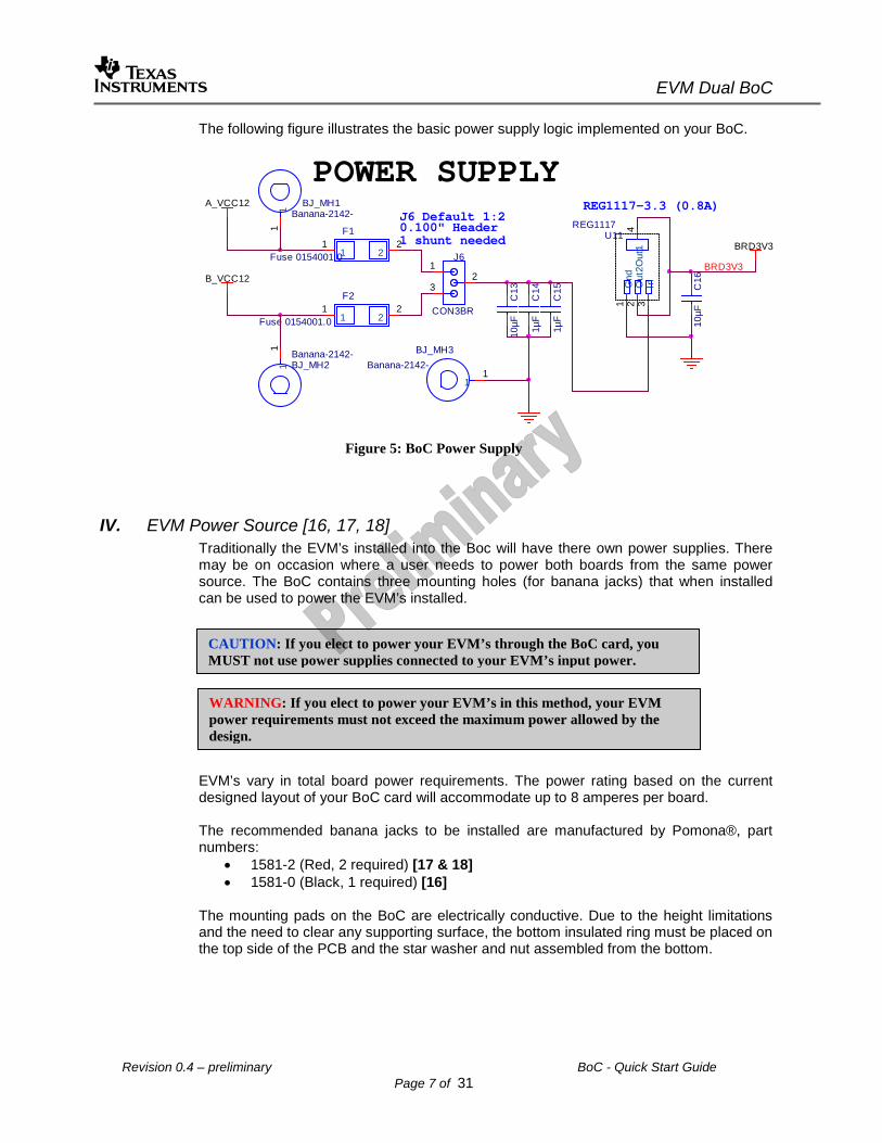
The following figure illustrates the basic power supply logic implemented on your BoC.
Figure 5: BoC Power Supply
IV. EVM Power Source [16, 17, 18] Traditionally the EVM’s installed into the Boc will have there own power supplies. There may be on occasion where a user needs to power both boards from the same power source. The BoC contains three mounting holes (for banana jacks) that when installed can be used to power the EVM’s installed. EVM’s vary in total board power requirements. The power rating based on the current designed layout of your BoC card will accommodate up to 8 amperes per board. The recommended banana jacks to be installed are manufactured by Pomona®, part numbers:
The mounting pads on the BoC are electrically conductive. Due to the height limitations and the need to clear any supporting surface, the bottom insulated ring must be placed on the top side of the PCB and the star washer and nut assembled from the bottom.
POWER SUPPLY
F1
Fuse 0154001.011
22
F2
Fuse 0154001.0 11
22
A_VCC12
B_VCC12
J6
CON3BR
12
3
0.100" Header1 shunt needed
REG1117-3.3 (0.8A)
BRD3V3
J6 Default 1:2
C14
1µF
C16
10µF
C15
1µF
BJ_MH1Banana-2142-1
1
BJ_MH2Banana-2142-
11 BJ_MH3
Banana-2142-
11
C13
10µF
U11REG1117
Gnd
1
Out
22
In3
Out
14
BRD3V3
CAUTION: If you elect to power your EVM’s through the BoC card, you MUST not use power supplies connected to your EVM’s input power.
WARNING: If you elect to power your EVM’s in this method, your EVM power requirements must not exceed the maximum power allowed by the design.
V. Emulation Interface [1] Your BoC contains a traditional Texas Instruments 60-pin emulation header (item 1). It should be noted that emulation voltages across the AMCC backplane are intended for 3.3Vdc. Your BoC has been designed so that the emulation interface is also 3.3V, before using this interface it will be necessary to confirm that your EVM’s can accommodate a 3.3V logic level without damage occurring.
The emulation interface of you BoC is daisy-chained. This means that the test data in and test data out pins are configured such that both boards are in the scan chan at all times. If you require separate control, use separate emulators directly connected to each respective EVM.
VI. SGMII Interface Your BoC in designed to support two (2) lanes of SGMII. The SGMII interface is connected between each board (A & B) in a manner that provides intercommunication. Board A transmit (TX) lanes 1:0 are routed to the receive (RX) lanes 1:0 of Board B, and Board A receive (RX) lanes 1:0 are routed to the transmit (TX) lanes 1:0 of Board B. There are no AC coupling capacitors on your BoC, it is assume that your EVM hardware has been properly designed and contains the appropriate AC coupling capacitors on the respective AC nets.
VII. PCIE Interface Your BoC in designed to support four (4) lanes of PCIe. The PCIe interface is connected between each board (A & B) in a manner that provides intercommunication. Board A transmit (TX) lanes 7:4 are routed to the receive (RX) lanes 7:4 of Board B, and Board A receive (RX) lanes 7:4 are routed to the transmit (TX) lanes 7:4 of Board B. There are no AC coupling capacitors on your BoC, it is assume that your EVM hardware has been properly designed and contains the appropriate AC coupling capacitors on the respective AC nets. In some cases a common or alternate PCIe clock may be required, where needed the BoC has the ability to provide a common PCIe REFCLK, refer to section XVI for details and configuration options.
WARNING: The Emulation Interface is intended to operate at 3.3V, Confirm that your EVM level shifts this into to correct DSP range before using this interface
CAUTION: Confirm that your EVM supports this interface and that the number of interfaces as well as the pinout locations is supported correctly.
CAUTION: Confirm that your EVM supports this interface and that the number of interfaces as well as the pinout locations is supported correctly.
VIII. SRIO (Serial RapidIO) Interface Your BoC in designed to support four (4) lanes of SRIO. The SRIO interface is connected between each board (A & B) in a manner that provides intercommunication. Board A transmit (TX) lanes 11:8 are routed to the receive (RX) lanes 11:8 of Board B, and Board A receive (RX) lanes 11:8 are routed to the transmit (TX) lanes 11:8 of Board B. There are no AC coupling capacitors on your BoC, it is assume that your EVM hardware has been properly designed and contains the appropriate AC coupling capacitors on the respective AC nets.
IX. AIF (Antenna Interface) Interface Your BoC in designed to support six (6) lanes of AIF. The AIF interface is connected between each board (A & B) in a manner that provides intercommunication. Board A transmit (TX) lanes 18:17 & 15:12 are routed to the receive (RX) lanes 18:17 & 15:12 of Board B, and Board A receive (RX) lanes 18:17 & 15:12 are routed to the transmit (TX) lanes 18:17 & 15:12 of Board B. There are no AC coupling capacitors on your BoC, it is assume that your EVM hardware has been properly designed and contains the appropriate AC coupling capacitors on the respective AC nets.
X. I2C interface [5, 9, 11, 23] Your BoC card is designed with EEPROMs sitting on the I2C bus for each EVM. Each EEPROM is isolated from the other and resides on the AMCC backplane bus to the respective EVM. From the factory, this interface to each respective EVM is electrically ready for use but not directly connected to the EVM’s. Prior to use, the series termination resistors (0ohm) are required to be installed. These resistors are designed in as SMT components, 0402 in size. The following figure illustrates the pin out for both EEPROM interface headers. These headers (JP4 & JP5) can be used to program the individual on board EEPROMs. Your EEPROMS are blank from Texas Instruments. JP5 is the interface and programming header for Board A, and JP4 is the interface and programming header for Board B.
1
2
[Pin 1] SCL
[Pin 2] SDA
Figure 6 - I2C Programming Header
Each EEPROM contains a dedicated switch used to define the address. This feature was added to allow the end user the ability to change the EEPROM address in the event there was address contention do to something else sitting on the same bus. An on indication is denoted as “0”. JP4 is default configured as 0x011, JP5 is default configured as 0x000. The following table is provided to illustrate the switch to eeprom address correlation.
CAUTION: Confirm that your EVM supports this interface and that the number of interfaces as well as the pinout locations is supported correctly.
CAUTION: Confirm that your EVM supports this interface and that the number of interfaces as well as the pinout locations is supported correctly.
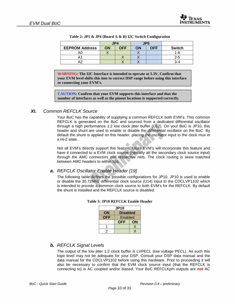
Table 2: JP5 & JP4 (Board A & B) I2C Switch Configuration
JP4 JP5 EEPROM Address ON OFF ON OFF Switch
A0 X X 1-6 A1 X X 2-5 A2 X X 3-4
XI. Common REFCLK Source Your BoC has the capability of supplying a common REFCLK both EVM’s. This common REFCLK is generated on the BoC and sourced from a dedicated differential oscillator through a high performance 1:2 low clock jitter buffer (U12). On your BoC is JP10, this header and shunt are used to enable or disable the differential oscillator on the BoC. By default the shunt is applied on this header, placing the oscillator input to the clock mux in a Hi-Z state. Not all EVM’s directly support this feature, future EVM’s will incorporate this feature and have it connected to a EVM clock source (typically att the secondary clock source input) through the AMC connectors and respective nets. The clock routing is skew matched between AMC headers to within 5ps.
a. REFCLK Oscillator Enable Header [19] The following table defines the possible configurations for JP10. JP10 is used to enable or disable the 30.72MHz differential clock source (U14) input to the CDCLVP1102 which is intended to provide a common clock source to both EVM’s for the REFCLK. By default the shunt is installed and the REFCLK source is disabled.
Table 3: JP10 REFCLK Enable Header
JP10 ON Disabled OFF Enabled
OFF ON 1 X 2 X
b. REFCLK Signal Levels The output of the low jitter 1:2 clock buffer is LVPECL (low voltage PECL). As such this logic level may not be adequate for your DSP. Consult your DSP data manual and the data manual for the CDCLVP1102 before using this hardware. Prior to proceeding it will also be necessary to confirm that the EVM clock source input (that the REFCLK is connecting to) is AC coupled and/or biased. Your BoC REFCLKp/n outputs are not AC
WARNING: The I2C Interface is intended to operate at 3.3V, Confirm that your EVM level shifts this into to correct DSP range before using this interface or connecting your EVM’s.
CAUTION: Confirm that your EVM supports this interface and that the number of interfaces as well as the pinout locations is supported correctly.
coupled, however they are biased. The current biasing scheme implemented is designed to provide the appropriate swing for most TI DSP’s available today. The following two figures illustrate the configuration for the REFCLK generation and biasing components. If a change in the output swing is needed, remove and replace the appropriate components carefully.
Figure 7: REFCLK Logic
Figure 8: REFCLK Biasing Components
C180.1µF
C190.01µF
U13, C18:C19 MUST be placed close to U3
R85:R86 are 0 ohm 0402 resistors,May need to be changed to 0.01uFCapacitors to AC couple
R850
R860
R84 must be across pins of U12
R80
150
R81
150
R82
150
R83
150
OUT A_REFCLK_P 3
OUT B_REFCLK_P 4
OUT A_REFCLK_N 3
OUT B_REFCLK_N 4
NO STUBSBRD3V3
JP10
HDR_1x2
12
R76
10K
0.100" Header1 shunt needed
J5 Default is Not Installed0 = Power Down (Hi-Z)1 = Normal (Active Output)
R7575
R6927
R7775R7875
BRD3V3
C120.01µF
R7975
R70150
R71
DN
IR
72D
NI
R73
DN
IR
74D
NI
U14
FXO-LC73
E/D1
NC2
GND3
+OUT4
-OUT5
Vdd6
U12CDCLVP1102
Gnd01
NC02
NC13
NC24
Vcc
5
INP
6
INN
7
Vac
ref
8
OUTP09OUTN010OUTP111OUTN112N
C3
13N
C4
14N
C5
15G
nd1
16G
P17
R84100
U12 Output is LVPECL Resistors R71:R75 & R77:R83have been configured for CML output. -Resistors will need to be changed to accommodate a different swing.-All resistors to go close to U12
XII. Timer0 Output Headers [12, 22] The BoC incorporates a separate single header connected (through the AMC B+ connector) to each EVM’s DSP’s Timer0 output pin [DSP Timer0_output BoC Timer0_output]. Header JP8 [22] is connected to Board B and header JP9 [12] is connected to Board A. This timer pin can be used to initiate a trigger event which is configurable using J5. Refer to section XVIII for additional configuration details. Your BoC is also provided with a custom 12”-14” (30.48cm – 35.46cm) jumper wire that can be used to connect between older EVM’s auxillary header containing the TimerOut0 pin to the either JP8 or JP9. This jumper is specifically designed with a 0.018” (0.457mm) male pin (on one side) that if used can be inserted into the appropriate location on the EVM auxillary header of you EVM, the opposite end contains a female header that is designed to attach to either JP8 or JP9. Refer to section XVIII for detailed information on configurations options.
XIII. Timer0 Input Header [10, 24] The BoC incorporates a separate single header connected (through the AMC B+ connector) to each EVM’s DSP’s Timer0 input pin [DSP Timer0_input BoC Timer0_input]. Header JP6 [10] is connected to Board B and header JP7 [24] is connected to Board A. This timer input pin to each respective DSP is provided for convience in the event future connection is required.
XIV. Common RP1CLK Source Your BoC has the capability of supplying a common RP1CLK both EVM’s. This common RP1CLK is generated on the BoC and sourced from a dedicated differential oscillator through a high performance 1:2 low clock jitter buffer (U1). On your BoC is JP1, this header and shunt are used to enable or disable the differential oscillator on the BoC. By default the shunt is applied on this header, placing the oscillator input to the clock mux in a Hi-Z state. Not all EVM’s directly support this feature, future EVM’s will incorporate this feature to allow for design debug, expandability and test. The clock routing is skew matched between AMC headers to within 5ps.
a. RP1CLK Oscillator Enable Header [8] The following table defines the possible configurations for JP1. JP1 is used to enable or disable the 30.72MHz differential clock source (U2) input to the CDCLVP1102 which is intended to provide a common clock source to both EVM’s for the RP1CLK. By default the shunt is installed and the RP1CLK source is disabled.
CAUTION: Different versions of EVM’s have different pinout configurations, confirm that your EVM supports this interface and feature.
CAUTION: Different versions of EVM’s have different pinout configurations, confirm that your EVM supports this interface and feature.
b. RP1CLK Signal Levels The output of the low jitter 1:2 clock buffer is LVPECL (low voltage PECL). As such this logic level may not be adequate for your DSP. Consult your DSP data manual and the data manual for the CDCLVP1102 before using this hardware. Prior to proceeding it will also be necessary to confirm that the EVM clock source input (that the REFCLK is connecting to) is AC coupled and/or biased. Your BoC RP1CLKp/n outputs are not AC coupled, however they are biased. The current biasing scheme implemented is designed to provide the appropriate swing for most TI DSP’s available today. The following two figures illustrate the configuration for the REFCLK generation and biasing components. If a change in the output swing is needed, remove and replace the appropriate components carefully.
Figure 9: RP1CLK Logic
R1310K
U1CDCLVP1102
Gnd01
NC02
NC13
NC24
Vcc5
INP6
INN7
Vacref8
OUTP09 OUTN0
10 OUTP111 OUTN112
NC313
NC414
NC515
Gnd116GP
17
JP1 Default Settings-Install shunt between 1-2-Oscillator output is Hi-Z
Zero stub between CON1/CON2 SMA and U2/U1 OScillator input, Nets must be identical length
CON1SMA_SMT
G12
G23
G34
G45 1
1
CON2SMA_SMT
G12
G23
G34
G451
1
U1 Output is LVPECL Resistors R20:R23 have been configured for CML output (mod for LVDS swing)
RP1CLK SMT SMA--Leave room for wrench---must be skew matched between SMA's and U10 input-NO STUBS
OUT A_DSP_RP1CLKP 3OUT A_DSP_RP1CLKN 3
C20.1µF
R2075R2175R2275R2375
C10.01µF
OUT B_DSP_RP1CLKP 3OUT B_DSP_RP1CLKN 3
BRD3V3
R1427
U3Ferrite1
12
2
C40.1µF
C50.01µF
R19150
BRD3V3
C310µF
U2
FXO-LC73
E/D1
NC2
GND3
+OUT4
-OUT5
Vdd6
R18
DN
I
R15
DN
IR
16D
NI
R17
DN
I
R28
150
R27
150
R26
150
R25
150
NOTE: PLACE OSCILLATOR WITH NO STUBS-U2 is a 30.72MHz Oscillator p/n FXO-LC735R-30.72 -By default leave Disabled-Oscillator only installed on limited board-RPICLKP/N nets to be matched length from "T"-R15:18, 20:23, & 25:28 must be placed close to output
R24 & R29 are 0 ohm 0402 resistors,May need to be changed to 0.01uFCapacitors to AC couple
c. Alternate RP1CLK Inputs [15] Your BoC has been designed with auxillary SMA input connectors (CON1 & CON2) in the event a different RP1CLK frequency is desired. Should you elect to utilize this input it will be necessary to confirm that it meets the input requirements of the CDCLVP1102 and that the corresponding outputs are properly biased, and that the oscillator is disabled (install JP1 shunt). CON1 is the negative polarity differential input; CON2 is the positive polarity differential input to the CDCLVP1102.
XV. Common TCLK_B Source Your BoC has the capability of supplying a common TCLK_B to both EVM’s. This common TCLK_B is generated on the BoC and sourced from a dedicated differential oscillator through a high performance 1:2 low clock jitter buffer (U6). On your BoC is JP2; this header and shunt are used to enable or disable the differential oscillator on the BoC. By default the shunt is applied on this header, placing the oscillator input to the clock mux in a Hi-Z state. Not all EVM’s directly support this feature, future EVM’s will incorporate this feature to allow for advanced clocking and test. The clock routing is skew matched between AMC headers to within 5ps.
a. TCLK_B Oscillator Enable Header [14] The AMC standard allows for external clock sources across the backplane bus, TCLK_x are several of the clocks allowed. The following table defines the possible configurations for JP2. JP2 is used to enable or disable the 30.72MHz differential clock source (U6) input to the CDCLVP1102 which is intended to provide a common clock source of
U1CDCLVP1102
0
VccINP6
INN7
Vacref8
OUTP09 OUTN0
10 OUTP111 OUTN112
NC313
NC414
NC515
Gnd1PZero stub between CON1/CON2 SMA and U2/U1 OScillator input, Nets must be identical length
CON1SMA_SMT
G12
G23
G34
G45 1
1
CON2SMA_SMT
G12
G23
G34
G451
1
CL
red od for LVDS swing)
RP1CLK SMT SMA--Leave room for wrench---must be skew matched between SMA's and U10 input-NO STUBS
OUT A_DSP_RP1CLKP 3OUT A_DSP_RP1CLKN 3
C20.1µF
R2075R2175R2275R2375 OUT B_DSP_RP1CLKP 3
OUT B_DSP_RP1CLKN 3
R18
DN
I
R15
DN
IR
16D
NI
R17
DN
I
R28
150
R27
150
R26
150
R25
150
R30100
BRD3V3
CAUTION: Different versions of EVM’s have different pinout configurations, confirm that your EVM supports this interface and feature.
30.72MHz to both EVM’s for TCLK_B. By default the shunt is installed and the REFCLK source is disabled.
Table 5: JP2 TCLK_B Enable Header
JP2 ON Disabled OFF Enabled
OFF ON 1 X 2 X
b. TCLK_B Signal Outputs [2, 13] There are two headers provided on your BoC; J1 & J2. Board A makes use of the 1 x 4 header whereas Board A interfaces with J2. In some current production TI EVM’s these pins are connected to the AMC headers, others not – confirm proper connection before powering up or using this feature. Due to layout constrainst J1 and J2 pinouts are not identical – please refer to the following figure and the silk screen on your BoC for proper pin locations.
J2
1TCLKA_P
TCLKA_N
TCLKB_P
TCLKB_N4
2
3
J1
1TCLKA_P
TCLKA_N
TCLKB_N
TCLKB_P4
2
3
Figure 11: TCLK_B Interface
The oscillator source (U5) is routed into the low jitter 1:2 clock buffer (U6), the output is a biased LVPECL (low voltage PECL). Some EVM input logic levels may have to be adjusted to properly interface with your DSP, consult your DSP data manual and the data manual for the CDCLVP1102 before using this hardware or making any modifications. Prior to proceeding it will also be necessary to confirm that the TCLK_B pins are not assigned other functions and that no contention will occur. Your BoC REFCLKp/n outputs are not AC coupled, however they are biased. The current biasing scheme implemented is designed to provide the appropriate swing for most TI DSP’s available today.
CAUTION: Different versions of EVM’s have different pinout configurations, confirm that your EVM supports this interface and feature.
The following two figures illustrate the configuration for the REFCLK generation and biasing components. If a change in the output swing is needed, remove and replace the appropriate components carefully.
Figure 12: TCLK_B Logic
Figure 13: TCLK_B Biasing Components
c. TCLK_A Signal Outputs [2, 13] Headers J1 & J2 are provided as a means of connecting the on board clock source to each respective DSP. TCLK_A is additionally provided on pins 1 & 2 of each header and routed to the respective pins on the AMC connectors. There is no logic attached to these pins which can be used to connect an alternate clock source into the DSP.
JP2 Default Settings-Install shunt-Oscillator output is Hi-Z
R31150
C70.01µF
OUTB_TCLKA_P4OUTB_TCLKA_N4
R33 27JP2
HDR_1x2
12
R36 & R41 are 0 ohm 0402 resistors, May need to be changed to 0.01uFCapacitors to AC couple
U6 Output is LVPECL Resistors R42:R45 have been configured for CML output
Before using this interface to your BoC, confirm the logic levels and terminations are correct.
XVI. Common PCIeREFCLK Source [25] Your BoC has the capability of supplying a common PCIeREFCLK to both EVM’s. This common PCIeREFCLK is generated on the BoC and sourced from a dedicated 25MHz crystal (U8) connected to a low noise crystal-to-HCSL clock generator (U7). On your BoC is JP3, this header and shunt are used to enable or disable the differential oscillator on the BoC. By default the shunt is applied on this header and the output disabled. Not all EVM’s directly support this feature, future EVM’s will incorporate this feature to allow for improved functionality and testing. The clock routing is skew matched between AMC headers to within 5ps.
a. PCIeREFCLK Crystal-to-HCSL Output Enable Header [25] The following table defines the possible configurations for JP3. JP3 is used to enable or disable the 25.00MHz differential output connected to each respective AMC header. By default the shunt is installed and the PCIEREFCLK output is disabled.
Table 6: JP3 PCIEREFCLK Enable Header
JP3 ON Disabled OFF Enabled
OFF ON 1 X 2 X
CAUTION: Different versions of EVM’s have different pinout configurations, confirm that your EVM supports this interface and feature.
b. PCIeREFCLK Logic The following figure illustrates the support logic for the PCIeREFCLK gerneration circuit
Figure 15: RP1CLK Logic
c. Alternate PCIeREFCLK Inputs [4] Your BoC has been designed with auxillary SMA input connectors (CON3 & CON4) in the event a different PCIeREFCLK frequency is desired. Should you elect to utilize this input it will be necessary to confirm that it meets the input requirements of the crystal-to-HCSL logic and that the corresponding outputs are properly biased, and that the crystal is removed.
XVII. RP1FB Source [7] In order to sync the RP1 clock with the RP1 frame bust interfaces to each EVM, your BoC has been designed with a direct interface. Provided are SMA connectors labeled as CON5 and CON6. Should you elect to utilize this RP1FB input it will be necessary to confirm that the signal provided meets the input requirements of the DSP and that the polarities are correct. CON5 is the negative polarity input; CON6 is the positive polarity input.
XVIII. RADSYNC & PHYSYNC Triggering [6] Your BoC has the ability to source a trigger and redirect it to an input on one or both DSP’s through the AMC header. The intention of this interface is to accept a timer event (trigger) from one EVM and redirect it to another making use of the PHYSYNC or RADSYNC pins. On future EVM’s the timer pins will be routed to the AMC backplane interface, until this is implemented the trigger event must be rerouted to the switch using the jumper wire provided (as described in section XII). Switch J5 has been included in the BoC allowing the ability to select from either DSP Timer0out signal and through various switch configurations redirecting it to either RADSYNC or PHYSYNC pin through the BoC AMC connector. The following figure illustrates the basic naming conventions assigned to the switch (J5).
R5010K
OUT A_PCIE_REF_CLK_P 3OUT A_PCIE_REF_CLK_N 3
NOTE: PLACE OSCILLATOR WITH NO STUBS-U5 is a 30.72MHz Oscillator p/n FXO-LC735R-30.72 -By default leave Disabled-RPICLKP/N nets to be matched length from "T"-R37:40, & 42:49 must be placed close to output
Pay attention to mounting requirements for all clock sourcesOUT B_PCIE_REF_CLK_P 3OUT B_PCIE_REF_CLK_N 3
R54475 1%
JP3
HDR_1x2
12
U7
NB3N5573
S01
S12
NC03
X14
X25
OE6
GND07
NC18
iREF9CLK1#10CLK111Vdd012GND113CLK0#14CLK015Vdd116
Common PCIe REFCLKSMT SMA-Leave room for wrench-No stubs and all "T's" must be balanced
Zero stub between CON5/CON4 SMA and U8/U7 Crystal input, Nets must be identical length-U7 configured for 100MHz outputU8 is a 25MHz xtal
U8Cry stal
11
22
C11
DN
I
R530
JP3 Default Settings-Install shunt between 1-2-Output is Hi-Z
Board A \ 1 GND Board A \ 170 GND Board A \ 2 12V Power Board A \ 169 TDI Board A \ 3 N/C Board A \ 168 TDO_2_TDI Board A \ 4 N/C Board A \ 167 TRST# Board A \ 5 N/C Board A \ 166 TMS Board A \ 6 N/C Board A \ 165 TCK Board A \ 7 GND Board A \ 164 GND Board A \ 8 N/C Board A \ 163 RP1CLKp Board A \ 9 12V Power Board A \ 162 RP1CLKn Board A \ 10 GND Board A \ 161 GND Board A \ 11 SGMII0_TXp Board A \ 160 SCL Board A \ 12 SGMII0_TXn Board A \ 159 SDA Board A \ 13 GND Board A \ 158 GND Board A \ 14 SGMII0_RXp Board A \ 157 RP1FBp Board A \ 15 SGMII0_RXn Board A \ 156 RP1FBn Board A \ 16 GND Board A \ 155 GND Board A \ 17 N/C Board A \ 154 PHYSYNC Con’t
NOTE: Your BoC Card contains ESD sensitive parts, proper ESD handling procedures are necessary
Board A \ 18 12V Power Board A \ 153 RADSYNC Board A \ 19 GND Board A \ 152 GND Board A \ 20 SGMII1_TXp Board A \ 151 AIF5_TXp Board A \ 21 SGMII1_TXn Board A \ 150 AIF5_TXn Board A \ 22 GND Board A \ 149 GND Board A \ 23 SGMII1_RXp Board A \ 148 AIF5_RXp Board A \ 24 SGMII1_RXn Board A \ 147 AIF5_RXn Board A \ 25 GND Board A \ 146 GND Board A \ 26 N/C Board A \ 145 AIF4_TXp Board A \ 27 12V Power Board A \ 144 AIF4_TXn Board A \ 28 GND Board A \ 143 GND Board A \ 29 N/C Board A \ 142 AIF4_RXp Board A \ 30 N/C Board A \ 141 AIF4_RXn Board A \ 31 GND Board A \ 140 GND Board A \ 32 N/C Board A \ 139 REFCLKp Board A \ 33 N/C Board A \ 138 REFCLKn Board A \ 34 GND Board A \ 137 GND Board A \ 35 N/C Board A \ 136 TIMER0OUT Board A \ 36 N/C Board A \ 135 TIMER0IN Board A \ 37 GND Board A \ 134 GND Board A \ 38 N/C Board A \ 133 AIF3_TXp Board A \ 39 N/C Board A \ 132 AIF3_TXn Board A \ 40 GND Board A \ 131 GND Board A \ 41 N/C Board A \ 130 AIF3_RXp Board A \ 42 12V Power Board A \ 129 AIF3_RXn Board A \ 43 GND Board A \ 128 GND Board A \ 44 PCIe4_TXp Board A \ 127 AIF2_TXp Board A \ 45 PCIe4_TXn Board A \ 126 AIF2_TXn Board A \ 46 GND Board A \ 125 GND Board A \ 47 PCIe4_RXp Board A \ 124 AIF2_RXp Board A \ 48 PCIe4_RXn Board A \ 123 AIF2_RXn Board A \ 49 GND Board A \ 122 GND Board A \ 50 PCIe5_TXp Board A \ 121 AIF1_TXp Board A \ 51 PCIe5_TXn Board A \ 120 AIF1_TXn Board A \ 52 GND Board A \ 119 GND Board A \ 53 PCIe5_RXp Board A \ 118 AIF1_RXp Board A \ 54 PCIe5_RXn Board A \ 117 AIF1_RXn Board A \ 55 GND Board A \ 116 GND Board A \ 56 N/C Board A \ 115 AIF0_TXp Board A \ 57 12V Power Board A \ 114 AIF0_TXn Board A \ 58 GND Board A \ 113 GND Board A \ 59 PCIe6_TXp Board A \ 112 AIF0_RXp Board A \ 60 PCIe6_TXn Board A \ 111 AIF0_RXn Board A \ 61 GND Board A \ 110 GND Board A \ 62 PCIe6_RXp Board A \ 109 SRIO4_TXp Board A \ 63 PCIe6_RXn Board A \ 108 SRIO4_TXn Board A \ 64 GND Board A \ 107 GND Board A \ 65 PCIe7_TXp Board A \ 106 SRIO4_RXp Board A \ 66 PCIe7_TXn Board A \ 105 SRIO4_RXn Board A \ 67 GND Board A \ 104 GND Board A \ 68 PCIe7_RXp Board A \ 103 SRIO3_TXp Board A \ 69 PCIe7_RXn Board A \ 102 SRIO3_TXn Board A \ 70 GND Board A \ 101 GND Con’t
Board A \ 71 N/C Board A \ 100 SRIO3_RXp Board A \ 72 12V Power Board A \ 99 SRIO3_RXn Board A \ 73 GND Board A \ 98 GND Board A \ 74 A_TCLK_Ap Board A \ 97 SRIO2_TXp Board A \ 75 A_TCLK_An Board A \ 96 SRIO2_TXn Board A \ 76 GND Board A \ 95 GND Board A \ 77 A_TCLK_Bp Board A \ 94 SRIO2_RXp Board A \ 78 A_TCLK_Bn Board A \ 93 SRIO2_RXn Board A \ 79 GND Board A \ 92 GND Board A \ 80 A_PCIEREFCLK_p Board A \ 91 SRIO1_TXp Board A \ 81 A_PCIEREFCLK_n Board A \ 90 SRIO1_TXn Board A \ 82 GND Board A \ 89 GND Board A \ 83 N/C Board A \ 88 SRIO1_RXp Board A \ 84 12V Power Board A \ 87 SRIO1_RXn Board A \ 85 GND Board A \ 86 GND
XXI. Pin Assignment [Board B] The following table is provided relative to the AMC piout assignment for your BoC card.
Board B \ 1 GND Board B \ 170 GND Board B \ 2 12V Power Board B \ 169 TDO_2_TDI Board B \ 3 N/C Board B \ 168 TDO Board B \ 4 N/C Board B \ 167 TRST# Board B \ 5 N/C Board B \ 166 TMS Board B \ 6 N/C Board B \ 165 TCK Board B \ 7 GND Board B \ 164 GND Board B \ 8 N/C Board B \ 163 RP1CLKp Board B \ 9 12V Power Board B \ 162 RP1CLKn Board B \ 10 GND Board B \ 161 GND Board B \ 11 SGMII0_TXp Board B \ 160 SCL Board B \ 12 SGMII0_TXn Board B \ 159 SDA Board B \ 13 GND Board B \ 158 GND Board B \ 14 SGMII0_RXp Board B \ 157 RP1FBp Board B \ 15 SGMII0_RXn Board B \ 156 RP1FBn Board B \ 16 GND Board B \ 155 GND Board B \ 17 N/C Board B \ 154 PHYSYNC Board B \ 18 12V Power Board B \ 153 RADSYNC Board B \ 19 GND Board B \ 152 GND Board B \ 20 SGMII1_TXp Board B \ 151 AIF5_TXp Board B \ 21 SGMII1_TXn Board B \ 150 AIF5_TXn Board B \ 22 GND Board B \ 149 GND Board B \ 23 SGMII1_RXp Board B \ 148 AIF5_RXp Board B \ 24 SGMII1_RXn Board B \ 147 AIF5_RXn Board B \ 25 GND Board B \ 146 GND Board B \ 26 N/C Board B \ 145 AIF4_TXp Board B \ 27 12V Power Board B \ 144 AIF4_TXn Board B \ 28 GND Board B \ 143 GND Con’t
Board B \ 29 N/C Board B \ 142 AIF4_RXp Board B \ 30 N/C Board B \ 141 AIF4_RXn Board B \ 31 GND Board B \ 140 GND Board B \ 32 N/C Board B \ 139 REFCLKp Board B \ 33 N/C Board B \ 138 REFCLKn Board B \ 34 GND Board B \ 137 GND Board B \ 35 N/C Board B \ 136 TIMER0OUT Board B \ 36 N/C Board B \ 135 TIMER0IN Board B \ 37 GND Board B \ 134 GND Board B \ 38 N/C Board B \ 133 AIF3_TXp Board B \ 39 N/C Board B \ 132 AIF3_TXn Board B \ 40 GND Board B \ 131 GND Board B \ 41 N/C Board B \ 130 AIF3_RXp Board B \ 42 12V Power Board B \ 129 AIF3_RXn Board B \ 43 GND Board B \ 128 GND Board B \ 44 PCIe4_TXp Board B \ 127 AIF2_TXp Board B \ 45 PCIe4_TXn Board B \ 126 AIF2_TXn Board B \ 46 GND Board B \ 125 GND Board B \ 47 PCIe4_RXp Board B \ 124 AIF2_RXp Board B \ 48 PCIe4_RXn Board B \ 123 AIF2_RXn Board B \ 49 GND Board B \ 122 GND Board B \ 50 PCIe5_TXp Board B \ 121 AIF1_TXp Board B \ 51 PCIe5_TXn Board B \ 120 AIF1_TXn Board B \ 52 GND Board B \ 119 GND Board B \ 53 PCIe5_RXp Board B \ 118 AIF1_RXp Board B \ 54 PCIe5_RXn Board B \ 117 AIF1_RXn Board B \ 55 GND Board B \ 116 GND Board B \ 56 N/C Board B \ 115 AIF0_TXp Board B \ 57 12V Power Board B \ 114 AIF0_TXn Board B \ 58 GND Board B \ 113 GND Board B \ 59 PCIe6_TXp Board B \ 112 AIF0_RXp Board B \ 60 PCIe6_TXn Board B \ 111 AIF0_RXn Board B \ 61 GND Board B \ 110 GND Board B \ 62 PCIe6_RXp Board B \ 109 SRIO4_TXp Board B \ 63 PCIe6_RXn Board B \ 108 SRIO4_TXn Board B \ 64 GND Board B \ 107 GND Board B \ 65 PCIe7_TXp Board B \ 106 SRIO4_RXp Board B \ 66 PCIe7_TXn Board B \ 105 SRIO4_RXn Board B \ 67 GND Board B \ 104 GND Board B \ 68 PCIe7_RXp Board B \ 103 SRIO3_TXp Board B \ 69 PCIe7_RXn Board B \ 102 SRIO3_TXn Board B \ 70 GND Board B \ 101 GND Board B \ 71 N/C Board B \ 100 SRIO3_RXp Board B \ 72 12V Power Board B \ 99 SRIO3_RXn Board B \ 73 GND Board B \ 98 GND Board B \ 74 A_TCLK_Ap Board B \ 97 SRIO2_TXp Board B \ 75 A_TCLK_An Board B \ 96 SRIO2_TXn Board B \ 76 GND Board B \ 95 GND Board B \ 77 A_TCLK_Bp Board B \ 94 SRIO2_RXp Board B \ 78 A_TCLK_Bn Board B \ 93 SRIO2_RXn Board B \ 79 GND Board B \ 92 GND Board B \ 80 A_PCIEREFCLK_p Board B \ 91 SRIO1_TXp Board B \ 81 A_PCIEREFCLK_n Board B \ 90 SRIO1_TXn Con’t
Board B \ 82 GND Board B \ 89 GND Board B \ 83 N/C Board B \ 88 SRIO1_RXp Board B \ 84 12V Power Board B \ 87 SRIO1_RXn Board B \ 85 GND Board B \ 86 GND
XXII. Header Intra-Connections The following table is provided to indicate the electrical connections between the two headers on your BoC.
Table 10: SerDes Board2Board Connections
Board Signal
Board Signal Board A \ 11 SGMII0_TXp Board B \ 14 SGMII0_RXp Board A \ 12 SGMII0_TXn Board B \ 15 SGMII0_RXn
Board A \ 14 SGMII0_RXp Board B \ 11 SGMII0_TXp Board A \ 15 SGMII0_RXn Board B \ 12 SGMII0_TXn Board A \ 20 SGMII1_TXp Board B \ 23 SGMII1_RXp Board A \ 21 SGMII1_TXn Board B \ 24 SGMII1_RXn Board A \ 23 SGMII1_RXp Board B \ 20 SGMII1_TXp Board A \ 24 SGMII1_RXn Board B \ 21 SGMII1_TXn
Board Signal
Board Signal Board A \ 44 PCIe4_TXp Board B \ 47 PCIe4_RXp Board A \ 45 PCIe4_TXn Board B \ 48 PCIe4_RXn Board A \ 47 PCIe4_RXp Board B \ 44 PCIe4_TXp Board A \ 48 PCIe4_RXn Board B \ 45 PCIe4_TXn
Board A \ 50 PCIe5_TXp Board B \ 53 PCIe5_RXp Board A \ 51 PCIe5_TXn Board B \ 54 PCIe5_RXn Board A \ 53 PCIe5_RXp Board B \ 50 PCIe5_TXp Board A \ 54 PCIe5_RXn Board B \ 51 PCIe5_TXn Board A \ 59 PCIe6_TXp Board B \ 62 PCIe6_RXp Board A \ 60 PCIe6_TXn Board B \ 63 PCIe6_RXn
Board A \ 62 PCIe6_RXp Board B \ 59 PCIe6_TXp Board A \ 63 PCIe6_RXn Board B \ 60 PCIe6_TXn Board A \ 65 PCIe7_TXp Board B \ 68 PCIe7_RXp Board A \ 66 PCIe7_TXn Board B \ 69 PCIe7_RXn Board A \ 68 PCIe7_RXp Board B \ 65 PCIe7_TXp Board A \ 69 PCIe7_RXn Board B \ 66 PCIe7_TXn
Board A \ 151 AIF5_TXp Board B \ 148 AIF5_RXp Board A \ 150 AIF5_TXn Board B \ 147 AIF5_RXn
Board A \ 148 AIF5_RXp Board B \ 151 AIF5_TXp Board A \ 147 AIF5_RXn Board B \ 150 AIF5_TXn Board A \ 145 AIF4_TXp Board B \ 142 AIF4_RXp Board A \ 144 AIF4_TXn Board B \ 141 AIF4_RXn Board A \ 142 AIF4_RXp Board B \ 145 AIF4_TXp Board A \ 141 AIF4_RXn Board B \ 144 AIF4_TXn
Board A \ 133 AIF3_TXp Board B \ 130 AIF3_RXp Board A \ 132 AIF3_TXn Board B \ 129 AIF3_RXn Board A \ 130 AIF3_RXp Board B \ 133 AIF3_TXp Board A \ 129 AIF3_RXn Board B \ 132 AIF3_TXn Board A \ 127 AIF2_TXp Board B \ 124 AIF2_RXp Board A \ 126 AIF2_TXn Board B \ 123 AIF2_RXn
Board A \ 124 AIF2_RXp Board B \ 127 AIF2_TXp Board A \ 123 AIF2_RXn Board B \ 126 AIF2_TXn Board A \ 121 AIF1_TXp Board B \ 118 AIF1_RXp Board A \ 120 AIF1_TXn Board B \ 117 AIF1_RXn Board A \ 118 AIF1_RXp Board B \ 121 AIF1_TXp Board A \ 117 AIF1_RXn Board B \ 120 AIF1_TXn
Board A \ 115 AIF0_TXp Board B \ 112 AIF0_RXp Board A \ 114 AIF0_TXn Board B \ 111 AIF0_RXn Board A \ 112 AIF0_RXp Board B \ 115 AIF0_TXp Board A \ 111 AIF0_RXn Board B \ 114 AIF0_TXn
Board Signal
Board Signal
Board A \ 109 SRIO4_TXp Board B \ 106 SRIO4_RXp Board A \ 108 SRIO4_TXn Board B \ 105 SRIO4_RXn Board A \ 106 SRIO4_RXp Board B \ 109 SRIO4_TXp Board A \ 105 SRIO4_RXn Board B \ 108 SRIO4_TXn Board A \ 103 SRIO3_TXp Board B \ 100 SRIO3_RXp Board A \ 102 SRIO3_TXn Board B \ 99 SRIO3_RXn
Board A \ 100 SRIO3_RXp Board B \ 103 SRIO3_TXp Board A \ 99 SRIO3_RXn Board B \ 102 SRIO3_TXn Board A \ 97 SRIO2_TXp Board B \ 94 SRIO2_RXp
Board Signal Board A \ 96 SRIO2_TXn Board B \ 93 SRIO2_RXn Board A \ 94 SRIO2_RXp Board B \ 97 SRIO2_TXp Board A \ 93 SRIO2_RXn Board B \ 96 SRIO2_TXn
Board A \ 91 SRIO1_TXp Board B \ 88 SRIO1_RXp Board A \ 90 SRIO1_TXn Board B \ 87 SRIO1_RXn Board A \ 88 SRIO1_RXp Board B \ 91 SRIO1_TXp Board A \ 87 SRIO1_RXn Board B \ 90 SRIO1_TXn
5
5
4
4
3
3
2
2
1
1
D D
C C
B B
A A
Board ASGMII [1]
TDO Output from Brd A to Brd B
Board AJTAG Interface
Board AClocks
Board ASGMII [0]
Board ARP1CLK
Board AAIF[0:5]
Board AAIF CLK & FS
Board AExpansion I2C
Board ASRIO[1:4]
Board APCIe[4:7]
FROM EVM A
TO EVM A
FROM EVM A
TO EVM A
FROM EVM A
TO EVM A
FROM EVM A
TO EVM A
FROM EVM A
TO EVM A
FROM EVM A
TO EVM A
FROM EVM A
TO EVM A
FROM EVM A
TO EVM A
FROM EVM A
TO EVM A
FROM EVM A
TO EVM A
FROM EVM A
TO EVM A
FROM EVM A
TO EVM A
FROM EVM A
TO EVM A
FROM EVM A
TO EVM A
FROM EVM A
TO EVM A
FROM EVM A
TO EVM A
TO EVM A
TO EVM A
TO EVM A
TO EVM A
CONNECTOR REFLECTS BACKPLANE PIN OUTS
TDITDO_2_TDITRST#TMSTCK
A_AMC0_SGMII1_TX_DPA_AMC0_SGMII1_TX_DN
A_AMC0_SGMII1_RX_DPA_AMC0_SGMII1_RX_DN
A_DSP_RP1CLKNA_DSP_RP1CLKP
A_AMCC_P7_PCIe_RX2PA_AMCC_P7_PCIe_RX2N
A_AMCC_P6_PCIe_RX1PA_AMCC_P6_PCIe_RX1N
A_AMCC_P7_PCIe_TX2PA_AMCC_P7_PCIe_TX2N
A_AMCC_P6_PCIe_TX1PA_AMCC_P6_PCIe_TX1N
A_AMCC_P13_AIF1_RXNA_AMCC_P13_AIF1_RXP
A_AMCC_P13_AIF1_TXPA_AMCC_P13_AIF1_TXN
A_AMCC_P14_AIF2_RXPA_AMCC_P14_AIF2_RXN
A_AMCC_P14_AIF2_TXPA_AMCC_P14_AIF2_TXN
A_AMCC_P15_AIF3_RXPA_AMCC_P15_AIF3_RXN
A_AMCC_P15_AIF3_TXPA_AMCC_P15_AIF3_TXN
A_AMCC_P12_AIF0_RXNA_AMCC_P12_AIF0_RXP
A_AMCC_P12_AIF0_TXPA_AMCC_P12_AIF0_TXN
A_AMCC_P17_AIF4_RXPA_AMCC_P17_AIF4_RXN
A_AMCC_P17_AIF4_TXPA_AMCC_P17_AIF4_TXN
A_AMCC_P18_AIF5_RXPA_AMCC_P18_AIF5_RXN
A_AMCC_P18_AIF5_TXPA_AMCC_P18_AIF5_TXN
A_AMC0_SGMII0_TX_DPA_AMC0_SGMII0_TX_DN
A_AMCC_P11_SRIO4_RXNA_AMCC_P11_SRIO4_RXP
A_AMCC_P9_SRIO2_TXNA_AMCC_P9_SRIO2_TXP
A_AMCC_P10_SRIO3_RXPA_AMCC_P10_SRIO3_RXN
A_AMCC_P8_SRIO1_TXNA_AMCC_P8_SRIO1_TXP
A_AMCC_P9_SRIO2_RXPA_AMCC_P9_SRIO2_RXN
A_AMCC_P11_SRIO4_TXPA_AMCC_P11_SRIO4_TXN
A_AMCC_P8_SRIO1_RXPA_AMCC_P8_SRIO1_RXN
A_AMCC_P10_SRIO3_TXPA_AMCC_P10_SRIO3_TXN
A_PCIE_REF_CLK_P
A_AMC0_SGMII0_RX_DPA_AMC0_SGMII0_RX_DN
A_PCIE_REF_CLK_N
A_AMCC_P5_PCIe_RX2PA_AMCC_P5_PCIe_RX2N
A_AMCC_P4_PCIe_RX1PA_AMCC_P4_PCIe_RX1N
A_AMCC_P5_PCIe_TX2PA_AMCC_P5_PCIe_TX2N
A_AMCC_P4_PCIe_TX1PA_AMCC_P4_PCIe_TX1N
A_TCLKA_PA_TCLKA_N
A_TCLKB_PA_TCLKB_N
A_REFCLK_PA_REFCLK_N
A_TIMEROUT_0A_TIMERIN_0
A_RP1FBPA_RP1FBN
A_DSP_SDA_AMCA_DSP_SCL_AMC
A_PHYSYNCA_RADSYNC
A_VCC12
INB_AMC0_SGMII1_TX_DP4INB_AMC0_SGMII1_TX_DN4
OUTA_AMC0_SGMII1_TX_DP4OUTA_AMC0_SGMII1_TX_DN4
IN TDI 7OUT TDO_2_TDI 4
IN TRST# 4,7IN TMS 4,7IN A_TCK 7
IN A_DSP_RP1CLKN 5IN A_DSP_RP1CLKP 5
OUTA_AMCC_P6_PCIe_TX1P4OUTA_AMCC_P6_PCIe_TX1N4
INB_AMCC_P6_PCIe_TX1P4INB_AMCC_P6_PCIe_TX1N4
INB_AMCC_P7_PCIe_TX2P4INB_AMCC_P7_PCIe_TX2N4
OUTA_AMCC_P7_PCIe_TX2P4OUTA_AMCC_P7_PCIe_TX2N4
INB_AMC0_SGMII0_TX_DP4INB_AMC0_SGMII0_TX_DN4
OUTA_AMC0_SGMII0_TX_DP4OUTA_AMC0_SGMII0_TX_DN4
OUTA_AMCC_P4_PCIe_TX1P4OUTA_AMCC_P4_PCIe_TX1N4
INB_AMCC_P4_PCIe_TX1P4INB_AMCC_P4_PCIe_TX1N4
INB_AMCC_P5_PCIe_TX2P4INB_AMCC_P5_PCIe_TX2N4
OUTA_AMCC_P5_PCIe_TX2P4OUTA_AMCC_P5_PCIe_TX2N4
INA_TCLKA_P5INA_TCLKA_N5
INA_TCLKB_P5INA_TCLKB_N5
INA_PCIE_REF_CLK_P5INA_PCIE_REF_CLK_N5
IN A_RP1FBN 6IN A_RP1FBP 6
IN A_RADSYNC 6IN A_PHYSYNC 6
IN B_AMCC_P18_AIF5_TXN 4IN B_AMCC_P18_AIF5_TXP 4
OUT A_AMCC_P17_AIF4_TXP 4OUT A_AMCC_P17_AIF4_TXN 4
IN B_AMCC_P17_AIF4_TXN 4IN B_AMCC_P17_AIF4_TXP 4
OUT A_AMCC_P18_AIF5_TXP 4OUT A_AMCC_P18_AIF5_TXN 4
OUT A_AMCC_P15_AIF3_TXP 4OUT A_AMCC_P15_AIF3_TXN 4
OUT A_AMCC_P14_AIF2_TXP 4OUT A_AMCC_P14_AIF2_TXN 4
IN B_AMCC_P15_AIF3_TXN 4IN B_AMCC_P15_AIF3_TXP 4
OUT A_AMCC_P13_AIF1_TXP 4OUT A_AMCC_P13_AIF1_TXN 4
IN B_AMCC_P14_AIF2_TXN 4IN B_AMCC_P14_AIF2_TXP 4
OUT A_AMCC_P12_AIF0_TXP 4OUT A_AMCC_P12_AIF0_TXN 4
IN B_AMCC_P13_AIF1_TXN 4IN B_AMCC_P13_AIF1_TXP 4
IN B_AMCC_P12_AIF0_TXN 4IN B_AMCC_P12_AIF0_TXP 4
OUT A_AMCC_P11_SRIO4_TXP 4OUT A_AMCC_P11_SRIO4_TXN 4
IN B_AMCC_P11_SRIO4_TXP 4IN B_AMCC_P11_SRIO4_TXN 4
OUT A_AMCC_P10_SRIO3_TXP 4OUT A_AMCC_P10_SRIO3_TXN 4
IN B_AMCC_P10_SRIO3_TXP 4IN B_AMCC_P10_SRIO3_TXN 4
OUT A_AMCC_P9_SRIO2_TXP 4OUT A_AMCC_P9_SRIO2_TXN 4
IN B_AMCC_P9_SRIO2_TXP 4IN B_AMCC_P9_SRIO2_TXN 4
OUT A_AMCC_P8_SRIO1_TXP 4OUT A_AMCC_P8_SRIO1_TXN 4
IN B_AMCC_P8_SRIO1_TXP 4IN B_AMCC_P8_SRIO1_TXN 4
BI A_AMC_EXP_SDA 6
OUT A_TIMERIN_0 6
IN A_AMC_EXP_SCL 6
IN A_TIMEROUT_0 6
IN A_REFCLK_N 7IN A_REFCLK_P 7
Title
Size Document Number Rev
Date: Sheet of
<Doc> E
LC_2-EVM_BoC-0002 - Board B Interface
B
3 10Friday, September 09, 2011
Title
Size Document Number Rev
Date: Sheet of
<Doc> E
LC_2-EVM_BoC-0002 - Board B Interface
B
3 10Friday, September 09, 2011
Title
Size Document Number Rev
Date: Sheet of
<Doc> E
LC_2-EVM_BoC-0002 - Board B Interface
B
3 10Friday, September 09, 2011
R3 DNIR4 DNI
R50R60
A1
AMC_BACKPLANE_CONNECTOR<Characteristic>
GND_11
GND_27
GND_310
PWR_12V_12
PS13
MP4
GA05
RSRVD66
RSRVD88
PWR_12V_29
Rx0+11
Rx0-12
GND_413
Tx0+14
Tx0-15
GND_516
GA117
PWR_12V_318
GND_619
Rx1+20
Rx1-21
GND_722
Tx1+23
Tx1-24
GND_825
GA226
PWR_12V_427
GND_928
Rx2+29
Rx2-30
GND_1031
Tx2+32
Tx2-33
GND_1134
Rx3+35
Rx3-36
GND_1237
Tx3+38
Tx3-39
GND_1340
ENABLE41
PWR_12V_542
GND_1443
Rx4+44
Rx4-45
GND_1546
Tx4+47
Tx4-48
GND_1649
Rx5+50
Rx5-51
GND_1752
Tx5+53
Tx5-54
GND_1855
SCL_L56
GND_1958
Rx6+59
Rx6-60
GND_2061
Tx6+62
Tx6-63
GND_2164
Rx7+65
Rx7-66
GND_2267
Tx7+68
Tx7-69
GND_2370
SDA_L71
PWR_12V_657
PWR_12V_772
GND_2473
TCLKA+74
TCLKA-75
GND_2576
TCLKB+77
TCLKB-78
GND_2679
FCLKA+80
FCLKA-81
GND_2782
PS083
PWR_12V_884
GND_2885
GND_2986Tx8-87Tx8+88
Rx8+91
Rx8-90
GND_3089
Tx9+94
Tx9-93
GND_3192
Rx9+97
Rx9-96
GND_3295
Tx10+100
Tx10-99
GND_3398
Rx10+103
Rx10-102
GND_34101
Tx11+106
Tx11-105
GND_35104
Rx11+109
Rx11-108
GND_36107
Tx12+112
Tx12-111
GND_37110
Rx12+115
Rx12-114
GND_38113
Tx13+118
Tx13-117
GND_39116
Rx13+121
Rx13-120
GND_40119
Tx14+124
Tx14-123
GND_41122
Rx14+127
Rx14-126
GND_42125
GND_43128
Tx15+130
Tx15-129
GND_44131Rx15-132Rx15+133GND_45134
TCLKC+136
TCLKC-135
TCLKD+139
TCLKD-138
GND_46137
Tx17+142
Tx17-141
GND_47140
Rx17+145
Rx17-144
GND_48143
Rx18+151
Rx18-150
GND_50149
Tx18+148
Tx18-147
GND_49146
Rx19+157
Rx19-156
GND_52155
Tx19+154
Tx19-153
GND_51152
Rx20+163
Rx20-162
GND_54161
Tx20+160
Tx20-159
GND_53158
GND_55164TCK165TMS166TRST167TDO168TDI169GND_56170
R10R20
5
5
4
4
3
3
2
2
1
1
D D
C C
B B
A A
Board BSGMII [1]
TDO Output from Brd A, TDI Input to Brd B
Board BJTAG Interface
Board BClocks
Board BSGMII [0]
Board BPCIe[4:7]
Board BRP1CLK
Board BAIF[0:5]
Board BAIF CLK & FS
Board BExpansion I2C
Board BSRIO[1:4]
TO EVM B
FROM EVM B
TO EVM B
FROM EVM B
TO EVM B
FROM EVM B
TO EVM B
FROM EVM B
TO EVM B
FROM EVM B
TO EVM B
FROM EVM B
TO EVM B
FROM EVM B
TO EVM B
FROM EVM B
TO EVM B
FROM EVM B
TO EVM B
FROM EVM B
TO EVM B
FROM EVM B
TO EVM B
FROM EVM B
TO EVM B
FROM EVM B
TO EVM B
FROM EVM B
TO EVM B
FROM EVM B
TO EVM B
FROM EVM B
TO EVM B
TO EVM B
TO EVM B
TO EVM B
TDO_2_TDITDOTRST#TMSTCK
B_AMC0_SGMII1_TX_DPB_AMC0_SGMII1_TX_DN
B_AMC0_SGMII1_RX_DPB_AMC0_SGMII1_RX_DN
B_AMC0_SGMII0_RX_DPB_AMC0_SGMII0_RX_DN
B_AMCC_P7_PCIe_RX2PB_AMCC_P7_PCIe_RX2N
B_AMCC_P6_PCIe_RX1PB_AMCC_P6_PCIe_RX1N
B_AMCC_P7_PCIe_TX2PB_AMCC_P7_PCIe_TX2N
B_AMCC_P6_PCIe_TX1PB_AMCC_P6_PCIe_TX1N
B_DSP_RP1CLKNB_DSP_RP1CLKP
B_AMCC_P13_AIF1_RXNB_AMCC_P13_AIF1_RXP
B_AMCC_P13_AIF1_TXPB_AMCC_P13_AIF1_TXN
B_AMCC_P14_AIF2_RXPB_AMCC_P14_AIF2_RXN
B_AMCC_P14_AIF2_TXPB_AMCC_P14_AIF2_TXN
B_AMCC_P15_AIF3_RXPB_AMCC_P15_AIF3_RXN
B_AMCC_P15_AIF3_TXPB_AMCC_P15_AIF3_TXN
B_AMCC_P12_AIF0_RXNB_AMCC_P12_AIF0_RXP
B_AMCC_P12_AIF0_TXPB_AMCC_P12_AIF0_TXN
B_AMCC_P17_AIF4_RXPB_AMCC_P17_AIF4_RXN
B_AMCC_P17_AIF4_TXPB_AMCC_P17_AIF4_TXN
B_AMCC_P18_AIF5_RXPB_AMCC_P18_AIF5_RXN
B_AMCC_P18_AIF5_TXPB_AMCC_P18_AIF5_TXN
B_AMC0_SGMII0_TX_DPB_AMC0_SGMII0_TX_DN
B_AMCC_P11_SRIO4_RXNB_AMCC_P11_SRIO4_RXP
B_AMCC_P9_SRIO2_TXNB_AMCC_P9_SRIO2_TXP
B_AMCC_P10_SRIO3_RXPB_AMCC_P10_SRIO3_RXN
B_AMCC_P8_SRIO1_TXNB_AMCC_P8_SRIO1_TXP
B_AMCC_P9_SRIO2_RXPB_AMCC_P9_SRIO2_RXN
B_AMCC_P11_SRIO4_TXPB_AMCC_P11_SRIO4_TXN
B_AMCC_P8_SRIO1_RXPB_AMCC_P8_SRIO1_RXN
B_AMCC_P10_SRIO3_TXPB_AMCC_P10_SRIO3_TXN
B_PCIE_REF_CLK_PB_PCIE_REF_CLK_N
B_AMCC_P5_PCIe_RX2PB_AMCC_P5_PCIe_RX2N
B_AMCC_P4_PCIe_RX1PB_AMCC_P4_PCIe_RX1N
B_AMCC_P5_PCIe_TX2PB_AMCC_P5_PCIe_TX2N
B_AMCC_P4_PCIe_TX1PB_AMCC_P4_PCIe_TX1N
B_TCLKA_PB_TCLKA_N
B_TCLKB_PB_TCLKB_N
B_REFCLK_PB_REFCLK_N
B_TIMEROUT_0B_TIMERIN_0
B_RP1FBPB_RP1FBN
B_EXP_SDAB_EXP_SCL
B_PHYSYNCB_RADSYNC
B_VCC12
INA_AMC0_SGMII1_TX_DP3INA_AMC0_SGMII1_TX_DN3
OUTB_AMC0_SGMII1_TX_DP3
IN TDO_2_TDI 3
OUTB_AMC0_SGMII1_TX_DN3
OUT TDO 7IN TRST# 3,7IN TMS 3,7IN B_TCK 7
OUTB_AMCC_P6_PCIe_TX1P3OUTB_AMCC_P6_PCIe_TX1N3
OUTB_AMCC_P7_PCIe_TX2P3OUTB_AMCC_P7_PCIe_TX2N3
INA_AMCC_P7_PCIe_TX2P3INA_AMCC_P7_PCIe_TX2N3
INA_AMCC_P6_PCIe_TX1P3INA_AMCC_P6_PCIe_TX1N3
IN B_DSP_RP1CLKN 5IN B_DSP_RP1CLKP 5
BI B_AMC_EXP_SDA 6IN B_AMC_EXP_SCL 6
OUT B_TIMERIN_0 6IN B_TIMEROUT_0 6
IN B_REFCLK_N 7IN B_REFCLK_P 7
INA_AMC0_SGMII0_TX_DP3INA_AMC0_SGMII0_TX_DN3
OUTB_AMC0_SGMII0_TX_DP3OUTB_AMC0_SGMII0_TX_DN3
OUTB_AMCC_P4_PCIe_TX1P3OUTB_AMCC_P4_PCIe_TX1N3
OUTB_AMCC_P5_PCIe_TX2P3OUTB_AMCC_P5_PCIe_TX2N3
INA_AMCC_P5_PCIe_TX2P3INA_AMCC_P5_PCIe_TX2N3
INA_AMCC_P4_PCIe_TX1P3INA_AMCC_P4_PCIe_TX1N3
INB_PCIE_REF_CLK_P5INB_PCIE_REF_CLK_N5
INB_TCLKA_P5INB_TCLKA_N5
INB_TCLKB_P5INB_TCLKB_N5
IN B_RP1FBN 6IN B_RP1FBP 6
IN B_RADSYNC 6IN B_PHYSYNC 6
IN A_AMCC_P18_AIF5_TXN 3IN A_AMCC_P18_AIF5_TXP 3
IN A_AMCC_P17_AIF4_TXP 3IN A_AMCC_P17_AIF4_TXN 3
OUT B_AMCC_P17_AIF4_TXP 3OUT B_AMCC_P17_AIF4_TXN 3
OUT B_AMCC_P18_AIF5_TXP 3OUT B_AMCC_P18_AIF5_TXN 3
IN A_AMCC_P14_AIF2_TXP 3IN A_AMCC_P14_AIF2_TXN 3
OUT B_AMCC_P14_AIF2_TXP 3OUT B_AMCC_P14_AIF2_TXN 3
IN A_AMCC_P15_AIF3_TXN 3IN A_AMCC_P15_AIF3_TXP 3
OUT B_AMCC_P15_AIF3_TXP 3OUT B_AMCC_P15_AIF3_TXN 3
IN A_AMCC_P12_AIF0_TXP 3IN A_AMCC_P12_AIF0_TXN 3
OUT B_AMCC_P12_AIF0_TXP 3OUT B_AMCC_P12_AIF0_TXN 3
IN A_AMCC_P13_AIF1_TXN 3IN A_AMCC_P13_AIF1_TXP 3
OUT B_AMCC_P13_AIF1_TXP 3OUT B_AMCC_P13_AIF1_TXN 3
OUT B_AMCC_P11_SRIO4_TXP 3OUT B_AMCC_P11_SRIO4_TXN 3
IN A_AMCC_P11_SRIO4_TXP 3IN A_AMCC_P11_SRIO4_TXN 3
OUT B_AMCC_P10_SRIO3_TXP 3OUT B_AMCC_P10_SRIO3_TXN 3
IN A_AMCC_P10_SRIO3_TXP 3IN A_AMCC_P10_SRIO3_TXN 3
OUT B_AMCC_P9_SRIO2_TXP 3OUT B_AMCC_P9_SRIO2_TXN 3
IN A_AMCC_P9_SRIO2_TXP 3IN A_AMCC_P9_SRIO2_TXN 3
OUT B_AMCC_P8_SRIO1_TXP 3OUT B_AMCC_P8_SRIO1_TXN 3
IN A_AMCC_P8_SRIO1_TXP 3IN A_AMCC_P8_SRIO1_TXN 3
Title
Size Document Number Rev
Date: Sheet of
<Doc> E
LC_2-EVM_BoC-0002 - Board B Interface
B
4 10Friday, September 09, 2011
Title
Size Document Number Rev
Date: Sheet of
<Doc> E
LC_2-EVM_BoC-0002 - Board B Interface
B
4 10Friday, September 09, 2011
Title
Size Document Number Rev
Date: Sheet of
<Doc> E
LC_2-EVM_BoC-0002 - Board B Interface
B
4 10Friday, September 09, 2011
R110R120
R70
R8 DNIR9
0
B1
AMC_BACKPLANE_CONNECTOR<Characteristic>
GND_11
GND_27
GND_310
PWR_12V_12
PS13
MP4
GA05
RSRVD66
RSRVD88
PWR_12V_29
Rx0+11
Rx0-12
GND_413
Tx0+14
Tx0-15
GND_516
GA117
PWR_12V_318
GND_619
Rx1+20
Rx1-21
GND_722
Tx1+23
Tx1-24
GND_825
GA226
PWR_12V_427
GND_928
Rx2+29
Rx2-30
GND_1031
Tx2+32
Tx2-33
GND_1134
Rx3+35
Rx3-36
GND_1237
Tx3+38
Tx3-39
GND_1340
ENABLE41
PWR_12V_542
GND_1443
Rx4+44
Rx4-45
GND_1546
Tx4+47
Tx4-48
GND_1649
Rx5+50
Rx5-51
GND_1752
Tx5+53
Tx5-54
GND_1855
SCL_L56
GND_1958
Rx6+59
Rx6-60
GND_2061
Tx6+62
Tx6-63
GND_2164
Rx7+65
Rx7-66
GND_2267
Tx7+68
Tx7-69
GND_2370
SDA_L71
PWR_12V_657
PWR_12V_772
GND_2473
TCLKA+74
TCLKA-75
GND_2576
TCLKB+77
TCLKB-78
GND_2679
FCLKA+80
FCLKA-81
GND_2782
PS083
PWR_12V_884
GND_2885
GND_2986Tx8-87Tx8+88
Rx8+91
Rx8-90
GND_3089
Tx9+94
Tx9-93
GND_3192
Rx9+97
Rx9-96
GND_3295
Tx10+100
Tx10-99
GND_3398
Rx10+103
Rx10-102
GND_34101
Tx11+106
Tx11-105
GND_35104
Rx11+109
Rx11-108
GND_36107
Tx12+112
Tx12-111
GND_37110
Rx12+115
Rx12-114
GND_38113
Tx13+118
Tx13-117
GND_39116
Rx13+121
Rx13-120
GND_40119
Tx14+124
Tx14-123
GND_41122
Rx14+127
Rx14-126
GND_42125
GND_43128
Tx15+130
Tx15-129
GND_44131Rx15-132Rx15+133GND_45134
TCLKC+136
TCLKC-135
TCLKD+139
TCLKD-138
GND_46137
Tx17+142
Tx17-141
GND_47140
Rx17+145
Rx17-144
GND_48143
Rx18+151
Rx18-150
GND_50149
Tx18+148
Tx18-147
GND_49146
Rx19+157
Rx19-156
GND_52155
Tx19+154
Tx19-153
GND_51152
Rx20+163
Rx20-162
GND_54161
Tx20+160
Tx20-159
GND_53158
GND_55164TCK165TMS166TRST167TDO168TDI169GND_56170
R10 DNI
5
5
4
4
3
3
2
2
1
1
D D
C C
B B
A A
Board BClocks
Board AClocks
CLOCK INTERFACERP1CLK SMT SMA--Leave room for wrench---must be skew matched between SMA's and U10 input-NO STUBS
Common PCIe REFCLKSMT SMA-Leave room for wrench-No stubs and all "T's" must be balanced
Zero stub between CON5/CON4 SMA and U8/U7 Crystal input, Nets must be identical length-U7 configured for 100MHz outputU8 is a 25MHz xtal
NOTE: PLACE OSCILLATOR WITH NO STUBS-U2 is a 30.72MHz Oscillator p/n FXO-LC735R-30.72 -By default leave Disabled-Oscillator only installed on limited board-RPICLKP/N nets to be matched length from "T"-R15:18, 20:23, & 25:28 must be placed close to output
JP1 Default Settings-Install shunt between 1-2-Oscillator output is Hi-Z
JP2 Default Settings-Install shunt-Oscillator output is Hi-Z
JP3 Default Settings-Install shunt between 1-2-Output is Hi-Z
R35 MUST be placed close to input pins of U6
U1 Output is LVPECL Resistors R20:R23 have been configured for CML output (mod for LVDS swing)
R24 & R29 are 0 ohm 0402 resistors,May need to be changed to 0.01uFCapacitors to AC couple
R30 must be across pins of U1
FULL SILK SCREENING REQUIRED
R36 & R41 are 0 ohm 0402 resistors, May need to be changed to 0.01uFCapacitors to AC couple
U6 Output is LVPECL Resistors R42:R45 have been configured for CML output
Zero stub between CON1/CON2 SMA and U2/U1 OScillator input, Nets must be identical length
NOTE: PLACE OSCILLATOR WITH NO STUBS-U5 is a 30.72MHz Oscillator p/n FXO-LC735R-30.72 -By default leave Disabled-RPICLKP/N nets to be matched length from "T"-R37:40, & 42:49 must be placed close to output
Pay attention to mounting requirements for all clock sources
BRD3V3
BRD3V3
BRD3V3
BRD3V3 BRD3V3
BRD3V3 BRD3V3
BRD3V3
OUTB_TCLKA_P4OUTB_TCLKA_N4
OUT A_PCIE_REF_CLK_P 3OUT A_PCIE_REF_CLK_N 3
OUT A_TCLKA_P 3OUT A_TCLKA_N 3
OUTB_TCLKB_P4OUTB_TCLKB_N4
OUTB_PCIE_REF_CLK_P4OUTB_PCIE_REF_CLK_N4
OUTB_DSP_RP1CLKP4OUTB_DSP_RP1CLKN4
OUT A_DSP_RP1CLKP 3OUT A_DSP_RP1CLKN 3
OUT A_TCLKB_N 3OUT A_TCLKB_P 3
Title
Size Document Number Rev
Date: Sheet of
<Doc> F
LC_2-EVM_BoC-0002 - Control Interface 1
B
5 10Tuesday, September 13, 2011
Title
Size Document Number Rev
Date: Sheet of
<Doc> F
LC_2-EVM_BoC-0002 - Control Interface 1
B
5 10Tuesday, September 13, 2011
Title
Size Document Number Rev
Date: Sheet of
<Doc> F
LC_2-EVM_BoC-0002 - Control Interface 1
B
5 10Tuesday, September 13, 2011
C10.01µF
R410
R26
150
R19150
U1CDCLVP1102
Gnd01
NC02
NC13
NC24
Vcc
5
INP
6
INN
7
Vac
ref
8
OUTP09OUTN010OUTP111OUTN112N
C3
13N
C4
14N
C5
15G
nd1
16G
P17
R47
150
R46
150
C10
0.1µ
F
R360
R27
150
C11
DN
I
R1427
JP3
HDR_1x2
12
R28
150
R4275
R3410K
R530
CON3SMA_SMTG1
2
G23
G34
G45
11
R4475
JP2
HDR_1x2
12
CON4SMA_SMTG1
2
G23
G34
G45
11
R4375
JP1
HDR_1x212
U2
FXO-LC73
E/D1
NC2
GND3
+OUT4
-OUT5
Vdd6
C310µF
C70.01µF
U6CDCLVP1102
Gnd01NC02NC13NC24
Vcc
5IN
P6
INN
7V
acre
f8
OUTP09
OUTN010
OUTP111
OUTN112
NC
313
NC
414
NC
515
Gnd
116
GP
17
U3Ferrite1
12
2
R2175
R18
DN
I
R1310K
R40
DN
I
R2375
R16
DN
I
R54475 1%
R33 27
R3210K
R52
20
R39
DN
I
CON2
SMA_SMT
G1
2
G2
3
G3
4
G4
51
1
R38
DN
I
R37
DN
I
R30100
U5
FXO-LC73
E/D1
NC2
GND3
+OUT4
-OUT5
Vdd6
C60.01µF
J2
CON4B
1234
R240
R31150
R290
R4575
CON1
SMA_SMT
G1
2
G2
3
G3
4
G4
5
11
C8
0.01
µF
C20.1µF
R35100
R2075
C50.01µF
U4Ferrite1
12
2
J1
CON4B
1234
R2275
R15
DN
I
C40.1µF
U7
NB3N5573
S01
S12
NC03
X14
X25
OE6
GND07
NC18
iREF9CLK1#10CLK111Vdd012GND113CLK0#14CLK015Vdd116
C9
10µF
R17
DN
I
R51
10K
R49
150
R25
150
R5010K
R48
150
U8Crystal
11
22
5
5
4
4
3
3
2
2
1
1
D D
C C
B B
A A
Board A i2cExpansion
Board AAIF CLK & FS
Zero stub length to resistors,Nets must be identical length
RP1FB / SMT SMA--Leave room for wrench--
Zero stub length to resistors,Nets must be identical length
J11 [ON = 0] DEFAULT1 - A0 OFF2 - A1 ON3 - A2 ON
J10 [ON = 0] DEFAULT 1 - A0 ON 2 - A1 ON 3 - A2 ON
Board B i2cExpansion
Board BAIF CLK & FS
FACTORY J9 SETTINGS 01 - 12 Board B RADSYNC - ON02 - 11 Board B PHYSYNC - ON03 - 01 Board A RADSYNC - OFF04 - 09 Board A PHYSYNC - OFF05 - 08 TimerOut 0 Board B - ON06 - 07 TimerOut 0 Board A - OFF
R73 &R32 are 0 ohm 0402 resistors,May need to be changed to 0.01uFCapacitors to AC couple CON5/CON6 net connections to R63/64
and R65/66 must be matched in length-lengths from resistor junctions to AMC headers must be identical
Placement of JP6/JP8 should be identical to JP7/JP9.-Placement of R67 should be identical in distance to R68 from Headers and switch
BRD3V3
BRD3V3
BRD3V3
BRD3V3
BRD3V3
BI A_AMC_EXP_SDA 3IN A_AMC_EXP_SCL 3
OUT A_RP1FBP 3OUT A_RP1FBN 3
BIB_AMC_EXP_SDA4INB_AMC_EXP_SCL4
OUTB_RP1FBN4OUTB_RP1FBP4
OUTB_TIMEROUT_04
INB_TIMERIN_04OUT A_TIMERIN_0 3
IN A_TIMEROUT_0 3
OUTB_RADSYNC4OUTB_PHYSYNC4 OUT A_PHYSYNC 3
OUT A_RADSYNC 3
Title
Size Document Number Rev
Date: Sheet of
<Doc> A
LC_2-EVM_BoC-0002 - Control Interface 2
B
6 10Friday, September 09, 2011
Title
Size Document Number Rev
Date: Sheet of
<Doc> A
LC_2-EVM_BoC-0002 - Control Interface 2
B
6 10Friday, September 09, 2011
Title
Size Document Number Rev
Date: Sheet of
<Doc> A
LC_2-EVM_BoC-0002 - Control Interface 2
B
6 10Friday, September 09, 2011
JP4
HDR_1x2
12
R6610
U10
EEPROM
A01
A12
A23
Vss4
SDA5SCL6WP7Vcc8
R6310
R6210K
R670
ON
J3
219-3MST
1234
56
ON J5SDA06H1SBD
1 2 3 4 5 67891012 11
CON6SMA_SMTG
12
G2
3
G3
4
G4
5
11
R680
JP8HDR_1x1
1
JP7HDR_1x1
1
R6510
ON
J4
219-3MST
123 4
56
JP6
HDR_1x1
1
R6110K
CON5SMA_SMT G
12
G2
3
G3
4
G4
51
1
R5810K
JP5
HDR_1x2
12
R6410
R5910K
R561K
R551K
JP9HDR_1x1
1
R6010K
R5710K
U9
EEPROM
A01
A12
A23
Vss4
SDA5 SCL6 WP7 Vcc8
5
5
4
4
3
3
2
2
1
1
D D
C C
B B
A A
Board A & BDaisy ChainJTAGInterface
TCKRTn total length to match TCK routing on EVM's (No stubs allowed, resistor connection should be as close to header pin as possible.
EMULATION INTERFACE
TVD Target PowerSupply for IO's
POWER SUPPLY
NOTE: Interface is 3.3V andrequires 3.3V level translationprior to interface with DSP. Thisis done to comply with the currentAMC specification
0.100" Header1 shunt needed
REG1117-3.3 (0.8A)
J6 Default 1:2
0.100" Header1 shunt needed
J5 Default is Not Installed0 = Power Down (Hi-Z)1 = Normal (Active Output)
TDI from Emulator to DSPTDO from DSP to Emulator
U12 Output is LVPECL Resistors R71:R75 & R77:R83have been configured for CML output. -Resistors will need to be changed to accommodate a different swing.-All resistors to go close to U12
U13, C18:C19 MUST be placed close to U3
R85:R86 are 0 ohm 0402 resistors,May need to be changed to 0.01uFCapacitors to AC couple
NO STUBS
R84 must be across pins of U12
BJ_MH3-Mounting hole to support Pamona 2142-0 (Black Banana Jack, Through hole)
BJ_MH1 & BJ_MH2-Mounting hole to support Pamona 2142-2 (Red Banana Jack, Through hole)
NOTE: Mounting holes are plated through, after plating, holes must support 6/32 mounting hardware and standoffs