PS/09/JXQR/078 23 December 2010 Rev C Ch 1 PS/09/JXQR/078 23 December 2010 Rev C Ch 1 This instruction as printed is an UNCONTROLLED COPY unless officially stamped and numbered as such and may not represent the latest revision. ELECTRO-OPTICAL TECHNOLOGY DIVISION (CODE JXQR) SPECIAL MISSIONS EO SYSTEMS BRANCH PERFORMANCE SPECIFICATION IMAGE INTENSIFIER ASSEMBLY, 18MM MICROCHANNEL WAFER HIGH PERFORMANCE TUBE MX-10160 GS 2 1
Transcript
PS/09/JXQR/07823 December 2010
Rev C Ch 1PS/09/JXQR/078
23 December 2010Rev C Ch 1
This instruction as printed is an UNCONTROLLED COPY unless officially stamped and numbered as such and may not represent the latest revision.
ELECTRO-OPTICAL TECHNOLOGY DIVISION (CODE JXQR)SPECIAL MISSIONS EO SYSTEMS BRANCH
1. Scope . This specification covers the Image Intensifier Assembly, 18mm Microchannel Wafer, High Performance Image Tube(see 5.1).
2. APPLICABLE DOCUMENTS
1. Government documents .
1. Specifications, standards, and handbooks . The following specifications, standards, and handbooks form a part of this document to the extent specified herein.
SPECIFICATIONS
DEPARTMENT OF DEFENSEMIL-PRF-49425
Aviator’s Night Vision Imaging System AN/AVS-6(V) ( )
STANDARDS
MIL-STD-810F ENVIRONMENTAL ENGINEERING CONSIDERATIONS AND LABORATORY TESTS
2. Other Government documents, drawings and publications . The following other Government documents, drawings and publications form a part of this document to the extent specified herein. All military and government specifications/standards, excluding MIL-PRF-49425, cited in the following documents are for reference only and do not form a part of the requirements therein.
DRAWINGS
NVESD
21
PS/09/JXQR/07823 December 2010
Rev C Ch 1PS/09/JXQR/078
23 December 2010Rev C Ch 1
A3256389 - Image Intensifier Tube, 18mm
2. Order of precedence . In the event of a conflict between the text of this document and the references cited herein, the text of this document takes precedence. Nothing in this document, however, supersedes applicable laws and regulations unless a specific exemption has been obtained.
3. REQUIREMENTS
1. Description . The Image Intensifier Tube, 18mm Microchannel Wafer, High Performance Image Tube herein referred to as the Assembly, shall employ a group III-V compound, semi-transparent photocathode sealed to a glass faceplate forming the input window to the assembly. The assembly shall contain a fiber optic inverter screen. The assembly shall include an integral power supply and be encapsulated within a hard surface insulating metallized envelope.
2. Thresholds. Performance parameters and features in this specification are assigned numerical or verbal values. All numerical and verbal values in this specification are Threshold requirements.
3. Certification. Unless otherwise specified by the contract, image intensifier assemblies furnished under this specification shall be products approved as compliant products (see 3.6.23).
1. Initial Production (IPT). The supplier shall furnish and test assemblies in accordance with requirements identified in 4.2. If the production assemblies are currently qualified on another DoD contract then IPT can waived as the assemblies may be qualified by similarity.
4. Construction . The Image Intensifier Assembly shall be constructed in accordance with the contract or purchase order, Drawing A3256389 and all the requirements of this specification.
1. Weight . The weight of the assembly shall not exceed 85 grams.
2. Parts and Materials . Parts and materials shall be as specified and as defined by the applicable drawing (see 3.4). The contractor shall select parts and materials which shall be capable of meeting all of the operational and environmental requirements specified. Any change of a part or material after certification requires notification of the
21
PS/09/JXQR/07823 December 2010
Rev C Ch 1PS/09/JXQR/078
23 December 2010Rev C Ch 1
procuring activity and submittal of proposed re-certification. Recovered materials shall be used to the maximum extent possible.
3. Phosphor screen . The phosphor screen shall be type P-43.
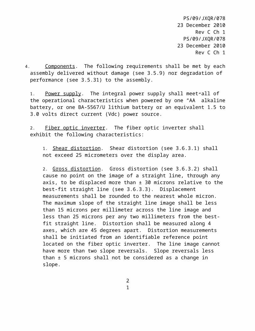
4. Components . The following requirements shall be met by each assembly delivered without damage (see 3.5.9) nor degradation of performance (see 3.5.31) to the assembly.
1. Power supply . The integral power supply shall meet all of the operational characteristics when powered by one “AA” alkaline battery, or one BA-5567/U lithium battery or an equivalent 1.5 to 3.0 volts direct current (Vdc) power source.
2. Fiber optic inverter . The fiber optic inverter shall exhibit the following characteristics:
1. Shear distortion . Shear distortion (see 3.6.3.1) shall not exceed 25 micrometers over the display area.
2. Gross distortion . Gross distortion (see 3.6.3.2) shall cause no point on the image of a straight line, through any axis, to be displaced more than ± 30 microns relative to the best-fit straight line (see 3.6.3.3). Displacement measurements shall be rounded to the nearest whole micron. The maximum slope of the straight line image shall be less than 15 microns per millimeter across the line image and less than 25 microns per any two millimeters from the best-fit straight line. Distortion shall be measured along 4 axes, which are 45 degrees apart. Distortion measurements shall be initiated from an identifiable reference point located on the fiber optic inverter. The line image cannot have more than two slope reversals. Slope reversals less than ± 5 microns shall not be considered as a change in slope.
3. Image inversion . The fiber optic inverter shall rotate a straight line image 180 ± 1 degree in a clockwise direction when viewed from the display side relative to the end points of the best-fit straight line (see 3.6.3.3). Image inversion measurements shall be rounded off to the nearest tenth of a degree.
4. Chicken wire . When the fiber optic is uniformly illuminated and viewed under 10 power magnification perpendicular to the plane surface, the fiber optic shall meet the chicken wire (see 3.6.4) limits specified in Table I.
21
PS/09/JXQR/07823 December 2010
Rev C Ch 1PS/09/JXQR/078
23 December 2010Rev C Ch 1
TABLE I. Fiber optic allowable chicken wire.
Number of allowable incidencesMinimum
length(inches)
Maximumlength
(inches) Chicken wire (zone 1) 0Disregard lengths which are not greater than 0.003 inches.
>0.003
----
Chicken wire (zone 2) 0 3 18 each spaced >0.035 inches apart. Disregard lengths which are not greater than 0.003 inches.
0.030 0.015 >0.003
>0.030 <0.030 <0.015
Chicken wire (zone 3) 0 6 12 Disregard lengths which are not greater than 0.019 inch.
0.045 0.030 >0.019
>0.045 <0.045 <0.039
Zone 1 - 0.295 inch diameter circle in center of optic.Zone 2 - 0.295 to 0.580 inch annulus concentric with Zone 1.Zone 3 - 0.580 to 0.710 inch annulus concentric with Zone 2.
3. Microchannel plate .
1. Ion barrier film quality (if necessary). There shall be no more than 10 type-B holes over the total useful area of the output screen. There shall be no more holes present with an effective diameter greater than 125 micrometers.
4. Input faceplate. The input faceplate shall be of optical quality with a minimum of a 60/40 (scratches/digs) finish and flat within 10 fringes using the sodium D light.
5. Chrome . There shall be no visible chrome present between the cathode and the black glass of the input faceplate.
6. System interface . When inserted into a certified ANVIS binocular assembly, the assembly shall operate and allow the objective lens to be focused from 28cm through
21
PS/09/JXQR/07823 December 2010
Rev C Ch 1PS/09/JXQR/078
23 December 2010Rev C Ch 1
infinity, and allow the eyepiece lens to be focused from +2 to -6 diopters. There shall be no flashing, flickering, or intermittent operation of the binocular.
7. Identification and marking . Each assembly shall be marked in accordance with drawing A3256389 as specified by customer.
8. Workmanship . The image intensifier assembly shall be free from burrs, chips, dirt, or any embedded or surface foreign material. Optical surfaces shall be free from imperfections that adversely affect the prescribed performance. Optical element surface quality shall be consistent with the best commercial practices.
5. Operational performance requirements . Unless otherwise specified herein, all operational performance requirements shall be complied without damage (see 3.5.9) nor degradation of performance (see 3.5.31).
a. The radiation source used for evaluation of photocathode sensitivity, EBI, luminance gain, signal-to-noise, output brightness uniformity, chrome, and reliability shall be a tungsten filament lamp operated at a color temperature of 2856 ± 50 Kelvin (K).
b. The radiation source used for evaluation of ion barrier film quality (if necessary), burn-in/ESS, temperature cycling, temperature extremes, environmentals, halo, bright source protection, fixed pattern noise, image alignment, resolution, MTF, useful cathode diameter, screen quality, luminance persistence, and EMI shall be a tungsten filament lamp operated at a color temperature of 2700K to 2900K.
c. The photometer used for screen brightness measurements shall be calibrated against a standard source as specified below:
(1) Tungsten filament lamp operated in conjunction with an opal glass or integrating sphere such that the color temperature of the radiation emitted from the opal glass or integrating sphere is 2856 ± 50K.
(2) Opal glass or integrating sphere to produce a uniform, Lambertian distribution.
(3) Corning spectral filters, nos. 3-71 and 4-67, or equivalent.
21
PS/09/JXQR/07823 December 2010
Rev C Ch 1PS/09/JXQR/078
23 December 2010Rev C Ch 1
(4) Output brightness of 0.1 to 1.0 foot-lamberts (fl) uniformly distributed over the output aperture.
d. Tolerances on radiation levels shall be ± 20 percent.
e. Meters used for monitoring lamp current and voltage shall have an accuracy of ± 0.25 percent.
f. Tests unless otherwise specified shall be performed at room temperature (see 3.6.7).
g. Neutral density filters used in test equipment shall have transmission characteristics with 10 percent of the nominal filter transmission from 0.35 to 1.0 micrometer.
h. Input voltage on the assembly shall be 3.0 ± 0.05 Vdc.
i. All gain and environmental tests except humidity shall be performed in a grounded housing.
j. Environmental test chambers shall maintain the temperature within ± 2°C of the specified test temperature.
k. All measurements of time shall be with a calibrated device capable of indicating a time variance one-half of the smallest increment required or smaller (i.e., requirement 1 second, indicator 0.5 second) and be calibrated to ± .010 of the required increment.
1. Photocathode sensitivity . Over a 16mm useful diameter circle with 0.001 lumen of radiation, the luminous transmission sensitivity shall be not less than 2,000 micro-amperes per lumen (µA/lm) with a voltage of not greater than 1200 Vdc applied to the photocathode. Over a 16mm useful diameter circle with filtered radiation between 1 x
10-8 to 5 x 10⁻⁶ watt, the radiant sensitivity shall be not less than 190 milliamperes/watt at 0.830 ± 0.001 micrometer and 80 milliamperes/watt at 0.880, ± 0.001 micrometer with a voltage not greater than 1200 Vdc applied to the photocathode.
2. Equivalent background input (EBI) . The equivalent background input at room temperature shall not exceed 3.0 x 10⁻¹¹ phot (lumens/square centimeter) when tested at 23°C +0/-2°C.
21
PS/09/JXQR/07823 December 2010
Rev C Ch 1PS/09/JXQR/078
23 December 2010Rev C Ch 1
3. Luminance gain . The assembly shall exhibit a room temperature luminance gain and high light level saturation characteristics per Table II.
TABLE II. Saturation requirements for luminance gain.
NominalLight input
(fc)
MinimumAllowable
Gain
Minimumallowableoutput (fl)
Maximumallowable
gain
Maximumallowableoutput (fl)
MaximumAllowable
input current (mA)
2 x 10⁻⁶
2 x 10⁻⁴
1.0 20.0
40K 10K NA NA
NA NA 2.5 2.5
80K 21K NA NA
NA NA 4.2 4.2
45 45 NA NA
4. Halo . The halo (see 3.6.8) produced by projecting light through an aperture and the AN/AVS-6(V)3 objective lens onto the input of the assembly, such that a 0.350 ± 0.02mm diameter spot is produced on the photocathode, shall be no greater than 1.0 mm in diameter. The illumination in the spot shall be not less that 5 x 10⁻⁴ foot-candle (fc). The illumination incident on the photocathode in the region outside the 0.350mm spot shall not exceed 5 x 10⁻⁷ fc.
5. Bright source protection . With operating potential applied, the assembly shall not be damaged (see 3.6.9) when subjected to an input illumination of not less than 50 milli-lumens concentrated on the photocathode within an area no greater than one square millimeter for a time interval not less than one minute. There shall be no discernible damage (see 3.6.9) after a non-operating period of not more than 24 hours.
6. Signal-to-noise ratio . The signal-to-noise (S/N) ratio (see 3.6.30) shall be a minimum of 25.0.
7. Fixed pattern noise .
1. Multi-to-multi pattern variation . With the operating potential applied to the assembly and the entire photocathode uniformly illuminated at a level of 1 to 2 x 10⁻⁴ fc, multi-to-multi brightness deviations from the mean value shall not exceed ± 10 percent.
2. Multi-boundary pattern noise . With the operating potential applied to the assembly and the entire photocathode uniformly illuminated at a level of 1 to 2 x 10⁻⁴ fc,
21
PS/09/JXQR/07823 December 2010
Rev C Ch 1PS/09/JXQR/078
23 December 2010Rev C Ch 1
the average value of the brightness deviations of the multi-boundary intensities shall not deviate from the mean value of the adjacent multi intensities by more than ± 10 percent. The mean value shall be established from the three adjacent multies containing the above multi-boundaries.
8. Output brightness uniformity . When the photocathode is uniformly illuminated with between 5 x 10⁻⁶ and 1 x 10⁻⁵ fc of light, the output brightness uniformity shall be such that the ratio of the maximum to minimum brightness variation over the useful screen area shall not exceed 3:1. For input illumination of 1 to 3 x 10⁻¹⁰ watt of radiation of wavelength 0.830 ± 0.001 micrometer, the ratio shall not exceed 3:1. Under the same conditions, when the screen is viewed with a 10-power magnifier, the background shading shall be uniformly graded with no distinct lines of demarcation between the light and dark areas.
9. Image alignment . With the operating potential applied and the photocathode illuminated to provide best contrast, a test reticle projected on the photocathode of the assembly concentric with the optical axis shall produce an image on the screen of the assembly such that the center of the reticle's image shall fall within a circle 0.006 inch in diameter concentric with the optical axis of the assembly.
10. Resolution .
1. Center resolution . The limiting resolution (see 3.6.16) of the assembly at the optical axis (see 3.5.15), referenced to the photocathode, shall not be less than 64 line pairs per millimeter (lp/mm).
2. Peripheral resolution . The limiting resolution (see 3.6.16) of the assembly at points along a 14mm diameter circle concentric with the optical axis (see 3.5.15), referenced to the photocathode, shall not be less than 57 lp/mm.
3. High light level center resolution . With the entire photocathode of the assembly illuminated with not less than 20 fc, the minimum center resolution shall be 36 lp/mm.
11. Modulation transfer function . With an input illumination of not greater than 8 x l0-4
fc, the minimum assembly modulation transfer function (MTF) (see 3.6.12) shall be as follows:
a. 61 percent MTF at 15.0 lp/mmb. 38 percent MTF at 25.0 lp/mm
21
PS/09/JXQR/07823 December 2010
Rev C Ch 1PS/09/JXQR/078
23 December 2010Rev C Ch 1
Measurement at the following two points shall be taken for information only:
c. MTF at 2.5 lp/mmd. MTF at 7.5 lp/mm
12. Useful cathode diameter . The useful cathode diameter shall be not less than 17.5mm.
13. Screen quality . With no light input to the assembly, observe and locate bright spots or discernible field emissions (see 3.6.13) on the screen when viewed with a 10-power magnifier. With 2 x 10⁻⁶ fc incident on the photocathode, there shall be no bright spots or discernible field emissions (see 3.65.13) brighter or larger than the background scintillations (see 3.6.14) on the screen when viewed with a 10-power magnifier. With the radiation level on the photocathode adjusted to obtain the best contrast, there shall be no bright spots visible on the screen when viewed with a 10-power magnifier except those identified as type B holes per 3.3.3.3.1. The dark spots which exceed a contrast (see 3.6.22) of 30 percent of their surrounding areas shall not exceed the sizes and quantities specified in Table III. If the spot is non-circular, the diameter of the circular spot of an equal area shall be used. When the distance between two spots is less than the maximum dimension of either spot, the two spots shall be considered as one circular spot whose diameter is equal to the sum of the maximum dimensions of the two spots plus the amount of separation between them. Graininess caused by grainy or "peppery" phosphor screen, channel-to-channel gain variations, or photocathode irregularities (see 3.6.20) shall not be discernible over the useful diameter to the degree that it detracts from normal operation, when viewed with a 10-power magnifier and with the photocathode uniformly illuminated. Screen quality shall also include any dirt, lint, hair, or red spots, which indicates phosphor contamination. No dirt, lint, hair, or red spots shall be visible on the screen when viewed with a 10-power magnifier.
TABLE III. Tube assembly dark spots.
Size of spots(inches)
Number ofSpots within0.22 inchdiametercircle
Number of spots within annulus bounded by 2 circles 0.22 and 0.58 inch diameter
Number of spots within annulus bounded by circles 0.58 inch diameter and total screen diameter
0.009 or larger 0 0 00.006 to 0.009 0 1 1
21
PS/09/JXQR/07823 December 2010
Rev C Ch 1PS/09/JXQR/078
23 December 2010Rev C Ch 1
0.003 to 0.006 0 2 2
NOTE: The 0.22 and 0.58 inch circles on the image screen shall be concentric with the optical axis of the assembly and the total number of spots in all zones shall not exceed four.
14. Luminance persistence . When an illumination of 4 x 10⁻³ fc is gated OFF, output brightness of the assembly shall fall to not greater than 0.15 percent within 300 milliseconds.
15. Veiling glare off-axis . The off-axis veiling glare (see 3.6.24) exhibited by the assembly in the AN/AVS-6 system shall not exceed the limits of Table IV when a point light source illuminates the objective’s entrance pupil at a level of 2.0 ± .5 x 10 -4 fc. The point source shall subtend less than 0.7 milli-radians. The average tube (phosphor) background brightness shall be less than or equal to 1.5 X 10⁻³ fl. The off-axis veiling glare requirement shall be from 2° to 70 beyond the field-of-view (FOV) of the objective lens.
TABLE IV. Off-axis veiling glare.
Point Source Angle(Degrees off Optical Axis)
Maximum Intensity ofVeiling Glare Image
(foot-lamberts)2 0.253 0.154 0.105 0.08
6 - 70 0.06
16. Environmental Characteristics . The assembly shall not be damaged (see 3.6.9) nor suffer degradation of performance (see 3.6.31) and shall meet the performance requirements specified herein when subjected to the following environmental conditions:
1. Environmental stress screening (ESS) . Each assembly shall be subjected to an appropriate ESS for the purpose of elimination of workmanship/infant mortality type failures (see 3.6.9).
21
PS/09/JXQR/07823 December 2010
Rev C Ch 1PS/09/JXQR/078
23 December 2010Rev C Ch 1
2. Vibration . The assembly, with no operating voltage applied, shall not be damaged nor suffer degradation of performance after being subjected to resonance search (see 3.6.21), resonance dwell, and cycling with vibrations of the frequency and amplitude represented in Figure 2 applied both parallel to and perpendicular to the optical axis of the assembly for not less than one (1) hour in each axis.
3. Shock . With no radiation incident on the photo-cathode, the operating assembly shall not be damaged nor suffer degradation of performance when subjected to 6 shock impacts parallel to the optical axis and 6 shock impacts perpendicular to the optical axis with no more than 2 flashes in each axis. Impacts shall be half-sine wave with a minimum peak amplitude of 75g's (see 3.6.5) and a duration of 6 ± 2 milliseconds measured at the 10 percent amplitude points.
4. Temperature extremes . The assembly shall meet the requirements specified in 3.5.16.1 and shall not be damaged nor suffer degradation of performance by continuous operation from +52°C to -37°C or operation after storage from +85°C to -37°C. The assembly shall not be damaged nor suffer degradation of performance by sudden temperature changes from +23°C to +85°C, +85C to +23and from +23°C to -37°C, -37 to +23 each transition occurring within five (5) minutes. Room temperature pre-test and room temperature post-test values shall be taken. Soak time at each temperature extreme shall be sufficient to attain temperature stabilization.
1. Operating requirements for +52°C and -37°C .
a. Input current - not greater than 57 mA at +52°C and 46 mA at -37°C.b. Gain at 2 x 10⁻⁶ fc - between 25,000 and 110,000 at both temperatures.c. Gain at 2 x 10⁻⁴ fc - between 10,000 and 24,000 at both temperatures. d. Operational stability at 1 FL tube output:
(1) For a period of 2 minutes after an initial operating time of 2 seconds, the output brightness shall not fluctuate more than +/- 10 percent from steady state and shall not drift more than +/- 15 percent from steady state. All fluctuations shall be random after the initial 2 seconds. There shall be no flickering, flashing, or blinking visible to the naked eye.
(2) Rise time (see 3.6.6) shall not be greater than 7 seconds and overshoot (see 3.6.17) shall not be greater than 40 percent of steady-state output brightness.
21
PS/09/JXQR/07823 December 2010
Rev C Ch 1PS/09/JXQR/078
23 December 2010Rev C Ch 1
e. Gain and EBI: The variation between the beginning of temperature testing room temperature pre-test gain, and the completion of temperature testing room temperature post-test gain shall not be greater than ± 20 percent. Post-test EBI shall be as specified in 3.6.2.
5. Humidity . The unprotected tube assembly shall not be damaged nor suffer degradation of performance when subjected to not less than 90 percent relative humidity at temperatures varying between 21°C and 65°C for a period of not less than 240 hours. The gain and input current shall not vary more than ± 20 percent, the equivalent background input (EBI) shall not exceed 3.0 x 10^(-11) lm/cm^2, and all parameters must remain within specified limits.
17. Electromagnetic interference (EMI) . The assembly, when properly incorporated within a certified AN/AVS-9 system shall be qualified by similarity with MIL-PRF-A3279453 (NVI) 03 May 2002.
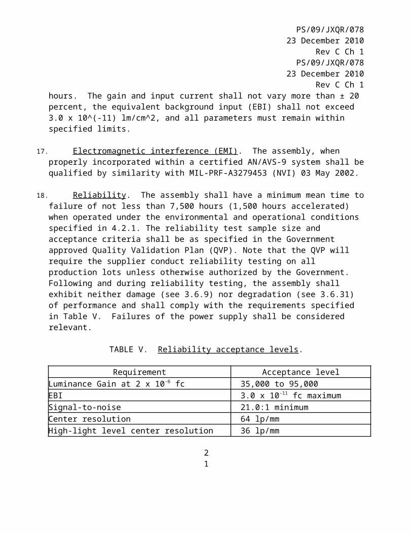
18. Reliability . The assembly shall have a minimum mean time to failure of not less than 7,500 hours (1,500 hours accelerated) when operated under the environmental and operational conditions specified in 4.2.1. The reliability test sample size and acceptance criteria shall be as specified in the Government approved Quality Validation Plan (QVP). Note that the QVP will require the supplier conduct reliability testing on all production lots unless otherwise authorized by the Government. Following and during reliability testing, the assembly shall exhibit neither damage (see 3.6.9) nor degradation (see 3.6.31) of performance and shall comply with the requirements specified in Table V. Failures of the power supply shall be considered relevant.
TABLE V. Reliability acceptance levels.
Requirement Acceptance levelLuminance Gain at 2 x 10⁻⁶ fc 35,000 to 95,000EBI 3.0 x 10⁻¹¹ fc maximumSignal-to-noise 21.0:1 minimumCenter resolution 64 lp/mmHigh-light level center resolution 36 lp/mmUseful cathode diameter 17.5 mm minimumOutput brightness uniformity per 3.5.8Screen quality per 3.5.13
21
PS/09/JXQR/07823 December 2010
Rev C Ch 1PS/09/JXQR/078
23 December 2010Rev C Ch 1
19. Storage life . The assembly shall exhibit neither damage (see 3.6.9) nor degradation of performance (see 3.6.31) during a storage period of not less than 60 days at room temperature (see 3.5.7) preceded by an exposure to 12 continuous temperature cycles of +85°C to -37°C. During cycling, the assembly shall remain at each temperature extreme until the assembly is thermally stabilized, and the chamber temperature rate of change shall be not less than 3°C per minute during transitions. As a minimum, conformance to the luminance gain, input current, signal-to-noise ratio, output brightness uniformity, screen quality, and useful cathode diameter requirements shall be verified upon completion of the 60 day storage period.
6. Technical interpretations . The following technical interpretations shall be, when referenced in section 3 mandatory for this specification.
1. Photocathode . The glass input window with a gallium arsenide substrate bonded to it is referred to as the photocathode.
2. Phosphor . The phosphor shall be type P-43 as defined commercially.
3. Distortion . The two types of distortion are shear distortion and gross distortion.
1. Shear distortion . Causes the image of a straight line to have a discrete, localized lateral displacement (break). Shear distortion is due to localized misalignment errors in the assembly of fibers or multifibers. Shear distortion in fiber bundles is sometimes referred to as incoherences.
2. Gross distortion . Causes the image of a straight line to curve. Gross distortion is caused by a long-range deformation of flow of fibers during fabrication.
3. Best-fit straight line . A straight line intersecting the +8 and -8 millimeter points of the input straight-line image. The +8 and -8 millimeter measurements are relative to the projected pattern center point.
4. Chicken wire . Defined as a predominant pattern of dead fibers, which has a diameter not greater than 0.0009 inch (2 single fibers) whose light transmission is so degraded that with light projected through the optic, single fibers in the area in question cannot be distinguished or identified as single fibers with the use of 50-power magnification.
5. "g" . A “g” is defined as a unit of gravitational force (on earth) to which an object is subjected.
21
PS/09/JXQR/07823 December 2010
Rev C Ch 1PS/09/JXQR/078
23 December 2010Rev C Ch 1
6. Rise time and decay time . The rise time required for the assembly to achieve 50 percent of its steady state performance after the voltage source is applied to the assembly. The decay time is the time required for the assembly to achieve the screen brightness not greater than 1 x 10⁻³ fl after the voltage source is disconnected.
7. Room temperature . Room temperature is defined as +23°C +10/-2°C.
8. Halo . Halo is defined as a circular area of bright-ness evidenced on the assembly output imaging screen occurring as a result of a small bright source input and concentric with the input.
9. Damage . Damage is defined as:
a. Electrical failure or malfunctioning, intermittent or continuous, including arcing, corona, flashing, bright spots, flickering, blinking, or a change in input current greater than ± 1.0 mA and more than 20 percent during or subsequent to completion of ESS testing and during the humidity testing.
b. Cracks, breakage, deformation, burrs, corrosion, or deterioration of any part or finish, and missing or loose components.
c. Imperfections in or on optical components that adversely affect optical performance.
10. Multi-to-multi pattern variation . Discernible spatial gain variation between individual multi-patterns or groups of multi-patterns.
11. Multi-boundary pattern noise . Discernible spatial gain variation between peripheral and interior channels or groups of channels in a multi-pattern.
12. Modulation transfer function (MTF) . Modulation transfer function is a measure of the degradation of an image as it appears at the output screen of the assembly as correlated to the input pattern which is normalized to 100 percent contrast at a spatial frequency equal to or less than 0.2 lines per millimeter.
13. Field emission . Discernible field emission is voltage-dependent extraneous emission, which appears as bright spots or a pattern that may flicker or appear intermittently on the image screen in one general area. Field emission is voltage
21
PS/09/JXQR/07823 December 2010
Rev C Ch 1PS/09/JXQR/078
23 December 2010Rev C Ch 1
dependent and is best observed with a low level of radiation incident on the photocathode.
14. Scintillations . Bright spots, which occur on the image screen randomly in space and time.
15. Optical axis . The optical axis of the assembly is defined as the mean centerline of that cylindrical portion of the assembly used to align the assembly in the system housing.
16. Limiting resolution . Limiting resolution is defined as the smallest resolution pattern for which the observer can see and distinguish between the black lines and the clear area between the black lines in both the vertical and horizontal test patterns.
17. Overshoot . The percent amplitude of output brightness above a steady-state condition at turn-on.
18. Type-B hole defect . When the photocathode of a packaged tube is illuminated with not less than 1 x 10⁻¹ fc, a type-B hole is a hole in the ion barrier which exists over a series of channels having an area equal to a circle with effective diameter not greater than 125 micrometers.
19. Useful area . The useful photocathode and phosphor screen area shall comprise a circle of diameter not less than 17.5 millimeters centered on the assembly optical axis.
20. Photocathode irregularities . Imperfections in the photocathode, which lead to significantly, degraded image quality. A photocathode grown on a host crystal cut more than 0.5 degree off the proper crystallographic axis, which leads to a terraced crystal surface; and hillocks or craters due to foreign inclusions in the crystal growth.
21. Resonant frequency . A resonant frequency is defined as any frequency where the response amplitude is greater than or equal to two times the input vibration amplitude at that frequency.
22. Contrast . Contrast is defined as B1 - B2. B1 + B2
B1 is the brightness surrounding the dark spot.B2 is the brightness of the dark spot.
21
PS/09/JXQR/07823 December 2010
Rev C Ch 1PS/09/JXQR/078
23 December 2010Rev C Ch 1
23. Compliant Product . For the purposes of this specification, a compliant product is a product that has successfully met all of the requirements of an IPT which verifies all requirements of this specification have been met. Should the supplier at any time make substantial changes in the process used to produce a compliant product for the Federal Government, the Government will determine what testing is necessary to verify continued compliance to specification requirements for all characteristics of the product affected by the changes.
24. Veiling glare . Veiling glare shall be defined as ghost images, crescents or other geometrically shaped images appearing in the system’s field-of-view, when a bright point source is outside the field-of-view and illuminating the entrance pupil of the objective lens.
25. Dirty window . A cosmetic defect in the gallium arsenide photocathode that reduces or impairs the image definition of the tube assembly.
26. Luminance transmission sensitivity . The photo current (in microamperes), corrected for leakage and dark current, divided by the actual input (in lumens).
27. Radiant sensitivity . Total tube current (minus photocathode leakage and dark current) divided by the actual input radiation (in watts).
28. EBI . EBI is defined as R1/(R2-R1) x actual input illumination where R1 is defined as the stabilized screen brightness (in fl) with no radiation incident on the photocathode and R2 is the screen brightness (in foot-lamberts) when the photocathode is illuminated by 3.5 to 7 x 10-11 phot (lumens/square cm) uniformly distributed over the full useful diameter centered on the photocathode faceplate. The angle of incident flux shall not be greater than 2 degrees from perpendicular such that the acceptance angle covers the full 17mm.
29. Luminance gain . When the photocathode of the operational tube assembly is illuminated with input light uniformly distributed over the full useful diameter of the faceplate, the luminance gain is defined as the screen luminance (in fl) divided by the actual input illumination (in fc) where screen luminance is measured such that the acceptance angle (of the measuring instrument) subtends a 17mm diameter area centered on the phosphor screen.
30. Signal-to-noise . Signal-to-noise is a measure of the image intensifier tube’s average output brightness (signal) divided by the standard deviation of output brightness (noise) per the following equation:
21
PS/09/JXQR/07823 December 2010
Rev C Ch 1PS/09/JXQR/078
23 December 2010Rev C Ch 1
S/N = (S0 - Sbkd)/K(N02 - Nbkd
2)0.5
where,
S = dc signalN = rms noiseS0 = average signal output from the S/N test setSbkd = average background signal from S/N test set with light input off
N0 = noise output from S/N test set rms meterNbkd = background noise from S/N test set rms meter
with light input off
K = correlation factor to obtain a S/N ratio over anequivalent bandwidth of 10 Hz independent of assembly frequency
response. K = 1.15 for a P-43 phosphor.
These statistics are measured with a specified input spot of light of 0.2-millimeter diameter placed within a 1-millimeter radius from the assembly optical axis, and at a light level of 1 x 10⁻⁵ fc of 2856 ± 50K black body irradiance. The standard deviation of brightness is measured over a 10-Hertz noise equivalent bandwidth.
31. Degradation of performance . Degradation of performance is defined as a cumulative change in measurable characteristics, which can result in failure of the assembly to meet specified requirements.
4. VERIFICATION
4.1 Applicability. For the purposes of confirming reliability and environmental compliance, the Government will accept existing qualifications issued under active U.S. Government contracts for image tubes built on the same production line in lieu of forming a unique test lot specific to this contract.
1. Classification of inspections . The inspection requirements specified herein are classified as follows:
a. Initial production testing (IPT) a. Conformance inspection (CI)
21
PS/09/JXQR/07823 December 2010
Rev C Ch 1PS/09/JXQR/078
23 December 2010Rev C Ch 1
2. Reliability test conditions .1. Environmental conditions . Samples selected for reliability verification shall first
demonstrate compliance to the requirements of shock (see 3.4.16.3), temperature extremes (see 3.4.16.4), and humidity (see 3.4.16.5). Reliability verification shall be conducted at a temperature not less than 40°C.
2. Operational conditions . The assemblies shall be continuously cycled for 11 minutes of ON time followed by 1 minute OFF. Input voltage to the assembly shall be 2.7 to 3.0 Vdc. Each assembly shall be continuously illuminated with not less than 5 x 10⁻⁵ fc. Once during each 11 minute period the illumination shall be increased to 5 x 10-
4 fc for 5 seconds, reduced to 5 x 10⁻⁵ fc for not less than 5 minutes, and then increased to 5 fc for not less than 3 seconds. Sufficient instrumentation shall be provided to ensure immediate recognition of a catastrophic failure as well as a change in output bright-ness. The assemblies shall remain on test until each assembly has completed 1,500 hours of operation; assemblies shall be removed from test conditions for not more than 15 hours at any given time for measurement of assembly parameters. Failed assemblies, which have been removed from test, shall not be replaced. 2. NOTES
(This section contains information of a general or explanatory nature that may be helpful, but is not mandatory).
1. Intended use . The assembly is intended for use in the following systems: AN/PVS-18 and AN/PVS-15 Night Vision Imaging Systems, electro-optical viewing devices capable of intensifying low light levels such that a visible image is presented for viewing purposes.
2. Certification requirements . With respect to products requiring certification, unless otherwise specified by the contract or purchase order, if a product is not certified at time of award, the contract shall require certification prior to first delivery. For the purposes of this specification, the activity responsible for approving certified products is the Night Vision and Electro Optics Department, Microwave Systems Directorate, Naval Surface Warfare Center, Crane Division.


![Illumination-Aware Age Progressionnovel illumination-aware age progression technique, lever-aging illumination modeling results [1,31], that properly account for scene illumination](https://static.documents.pub/doc/80x56/5e72745a0ac7de5cbf4199be/illumination-aware-age-progression-novel-illumination-aware-age-progression-technique.jpg)


