austriamicrosystems AG is now ams AG The technical content of this austriamicrosystems datasheet is still valid. Contact information: Headquarters: ams AG Tobelbaderstrasse 30 8141 Unterpremstaetten, Austria Tel: +43 (0) 3136 500 0 e-Mail: [email protected]Please visit our website at www.ams.com
Transcript
austriamicrosystems AG
is now
ams AG The technical content of this austriamicrosystems datasheet is still valid.
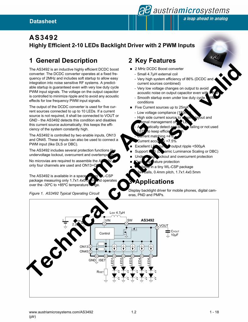
1 General DescriptionThe AS3492 is an inductive highly efficient DCDC boost converter. The DCDC converter operates at a fixed fre-quency of 2MHz and includes soft startup to allow easy integration into noise sensitive RF systems. A predict-able startup is guaranteed even with very low duty cycle PWM input signals. The voltage on the output capacitor is controlled to minimize ripple and to avoid any acoustic effects for low frequency PWM input signals.
The output of the DCDC converter is used for five cur-rent sources connected to up to 10 LEDs. If a current source is not required, it shall be connected to VOUT or GND - the AS3492 detects this condition and disables this current source automatically; this keeps the effi-ciency of the system constantly high.
The AS3492 is controlled by two enable inputs, ON13 and ON45. These inputs can also be used to connect a PWM input (like DLS or DBC).
The AS3492 includes several protection functions like undervoltage lockout, overcurrent and overtemperature.
No microvias are required to assemble the AS3492 if only four channels are used and ON13=ON45.
The AS3492 is available in a space-saving WL-CSP package measuring only 1.7x1.4x0.5mm and operates over the -30ºC to +85ºC temperature range.
Figure 1. AS3492 Typical Operating Circuit
2 Key Features2 MHz DCDC Boost converter
- Small 4.7µH external coil- Very high system efficiency of 86% (DCDC and
current sources combined)- Very low voltage changes on output to avoid
acoustic noise on output capacitor even with PWM - Smooth startup even under low duty cycle PWM
conditions
Five Current sources up to 25mA
- Low voltage compliance (150mV)- High side current source to simplify layout and
thermal management of the LEDs- Automatically detect and disable failing or not used
LEDs to keep efficiency high- Current matching <4% - Current accuracy <7.5%
Excellent LED current output ripple <500µA
Support DLS (Dynamic Luminance Scaling or DBC)
Undervoltage lockout and overcurrent protection
Overtemperature protection
Available in a tiny WL-CSP package
- 3x4 balls, 0.4mm pitch, 1.7x1.4x0.5mm
3 ApplicationsDisplay backlight driver for mobile phones, digital cam-eras, PND and PMPs.
����
����� �
�����
�� �
����
��� � ����
�����
��� ����
��
��
���
��
��
��
��
��
�
��
��
�������
����
AS3492
ams A
G
Technica
l conten
t still
valid
www.austriamicrosystems.com/AS3492 1.2 2 - 18
AS3492Datasheet - P inout
4 PinoutPin Assignment
Figure 2. Pin Assignments (Top View)
Pin Description
Table 1. WL-CSP12 Pin Description
Pin Number Pin Name Description
A1 VINPositive supply voltage input - connect to supply and make a short connection to input capacitor CVIN
A2 ISETExternal current set resistor, forced to 1.25V in operation - LED current typically 400xISET current
A3 LED1 Current source output 1 - controlled by ON13
B1 ON13 Digital input pin - enable input active high for current sources D1...D31
1. If ON13 and ON45 are low, the AS3492 enters shutdown.
B2 ON45 Digital input pin - enable input active high for current sources D4...D51,2
B3 LED2 Current source output 2 - controlled by ON13
C1 GNDSupply ground - connect to supply and make a short connection to input capacitor CVIN and CVOUT
C2 LED5 Current source output 5 - controlled by ON45
C3 LED3 Current source output 3 - controlled by ON13
D1 SW DCDC converter switching node
D2 VOUT DCDC converter output - make a short connection to capacitor COUT
D3 LED4 Current source output 4 - controlled by ON45
����������� �
������
������
�����
������
������
������
������
������
�����
������
������
����
������
������
�������������
�����
������
������
������
������
������
������
������
� ���
AS3492
AS3492
ams A
G
Technica
l conten
t still
valid
www.austriamicrosystems.com/AS3492 1.2 3 - 18
AS3492Datasheet - Abso lu te Max imum Rat ings
5 Absolute Maximum RatingsStresses beyond those listed in Table 2 may cause permanent damage to the device. These are stress ratings only, and functional operation of the device at these or any other conditions beyond those indicated in Table 3, “Electrical Characteristics,” on page 4 is not implied. Exposure to absolute maximum rating conditions for extended periods may affect device reliability.
Table 2. Absolute Maximum Ratings
Parameter Min Max Units Comments
VIN, ON13, ON45 and ISET to GND -0.3 +7.0 V
ON13, ON45 and ISET to VIN +0.3 V internal protection diodes to VIN
SW, VOUT, LED1...LED5 to GND -0.3 11 V
SW, LED1...LED5 to VOUT +0.3 V internal protection diodes to VOUT
Input Pin Current without causing latchup -100 +100+IIN mA Norm: EIA/JESD78
Continuous Power Dissipation (TA = +70ºC)
Continuous power dissipation 870 mW PT1 at TAMB=70ºC
1. Depending on actual PCB layout and PCB used
Continuous power dissipation derating factor 11.67 mW/ºC PDERATE2
2. PDERATE derating factor changes the total continuous power dissipation (PT) if the ambient temperature is not 70ºC. Therefore for e.g. TAMB=85ºC calculate PT at 85ºC = PT - PDERATE * (85ºC - 70ºC)
Electrostatic Discharge
ESD HBM ±2000 V Norm: JEDEC JESD22-A114F
ESD CDM ±500 V Norm: JEDEC JESD 22-C101E
ESD MM ±100 V Norm: JEDEC JESD 22-A115-B
Temperature Ranges and Storage Conditions
Junction Temperature +125 ºC
Storage Temperature Range -55 +125 ºC
Humidity 5 85 % Non condensing
Body Temperature during Soldering +260 ºC according to IPC/JEDEC J-STD-020
Moisture Sensitivity Level (MSL) MSL 1 Represents a max. floor life time of unlimited
ams A
G
Technica
l conten
t still
valid
www.austriamicrosystems.com/AS3492 1.2 4 - 18
AS3492Datasheet - E lec t r i ca l Charac te r i s t i cs
6 Electrical CharacteristicsVVIN = +2.5V to +5.5V, TAMB = -30ºC to +85ºC, unless otherwise specified. Typical values are at VVIN = +3.7V, TAMB = +25ºC, unless otherwise specified.
Table 3. Electrical Characteristics
Symbol Parameter Condition Min Typ Max Unit
General Operating Conditions
VVIN Supply Voltage 2.5 3.7 5.5 V
VVIN_REDUCED
Supply Voltage reduced performance not all parameters within specification 2.3 V
ISHUTDOWN Shutdown Current ON13=0V, ON45=0V 0.5 2.0 µA
IVIN Operating Current no load, PWM Normal mode 250 µA
TAMBOperating
Temperature -30 25 85 ºC
DCDC Converter parameters
VVOUT Output Voltage VOUT automatically regulated VVIN+0.3V
VVOUT_MAX
V
all other conditions with ON13=ON45 140
VVOUT_RIPPLE_PWM
Voltage VOUT due to PWM signal
identical signal for ON13 and ON45; DCDC not in pulseskip or current limit 70 mV
ILOAD Load current VOUT<7.5V 0.0 100 mA
Overall EfficiencyVVIN=3.7V, TAMB = +25ºC, LED mismatch <= 30mV,
VLED=3.0V
ILOAD=50mA 86
%ILOAD=75mA 85 86
ILOAD=100mA 86
fCLK Operating Frequency All internal timings are derived from this oscillator -10% 2.0 +10% MHz
tMIN_ON Minimum on-time 60 ns
MDC Maximum Duty Cycle 90 %
RSW_PDCDC Switch SW - VOUT 0.5
RSW_NDCDC Switch
SW - GND 0.5
Output voltage soft start
tVOUT_START softstart time measured from first high signal on ON13 or ON45 1.2 ms
VVOUT_START
VOUT startup voltage 7.0 V
tPWM_START_MAX
Startup with PWM Maximum duration between PWM pulses during startup; see Figure 17 on page 11 10 11 12 ms
tTIMEOUT DCDC timeout time if ON13 and ON45=0 for tTIMEOUT, the DCDC is stopped and the AS3492 enters shutdown 29 48 ms
Current Sources
VLED1..5LED1...LED5 output
voltage range2.6x2
3.3x2
3.9x2 V
ILED1..5LED1...LED5 output
current range 0.0 25.0 mA
ILED1..5LED1...LED5 current
source accuracy1 ILED1..5 =20mA -7.5 +7.5 %
ams A
G
Technica
l conten
t still
valid
www.austriamicrosystems.com/AS3492 1.2 5 - 18
AS3492Datasheet - E lec t r i ca l Charac te r i s t i cs
ILED1..5MATCH
LED1...LED5 current source matching ILED1..5 = 20mA -4.0 +4.0 %
ILED1..5RIPPLE
LED1...LED5 ripple current BW=10MHz
ILED > 5mA 10 % of ILED
ILED < 5mA 500 µA
ILED1..5PWMLIN
LED1...LED5
linearity2
ILED=20mA,PWM frequency 300Hz
PWM>=25/255 -2 +2 %
25/255>PWM>=1/255 -10 +10 %
fPWM PWM input frequency on pin ON13 or ON45 100 300 800 Hz
ILED1..5LEAKAGE
LED1...LED5 leakage current current source off, TAMB < +50ºC -0.5 0 +0.5 µA
VILED_COMP LED1...LED5 current
source voltage compliance
Minimum voltage between pin VOUT and
LED1...LED5, ILED<20mA3 100 mV
Current Reference (pin ISET)
VISET ISET voltage 1.25 V
ILED2ISETLED current to
ISETcurrent 400 A/A
Protection Functions (see page 12)
VVOUT_MAXVOUT overvoltage
protection 8.6 10.0 V
VVOUT_OPENLED
VOUT open LED detection threshold
Voltage level on VOUT where open LED detection is performed 8.0 8.5 8.8 V
VLED_OPENVVLED1..5 open
detection
an open LED is assumed if the voltage on the current source is less than VLED_OPEN and
VOUT=VVOUT_OPENLED92 125 mV
VLED_SHORTVLED1..5 short
detectionvoltage on LED1..5 where a shorted LED is
assumed 0.95 V
tLED_ERROR_DEB_OPEN
VLED1..5 open debounce time Open LED detection debounce time 4.8 µs
tLED_ERROR_DEB_SHORT
VLED1..5 short debounce time Short LED detection debounce time
4 9.0 µs
ILIMITCurrent Limit for coil
LSW (Pin SW) 510 600 685 mA
TOVTEMPOvertemperature
ProtectionJunction temperature
144 ºC
TOVTEMPHYST
Overtemperature Hysteresis 5 ºC
VUVLO Undervoltage LockoutFalling VVIN 1.8 1.9 2.1 V
Rising VVINVUVLO+0.05 2.2 2.3 V
Digital Interface
VIHHigh Level Input
Voltage 1.07 VVIN V
VILLow Level Input
Voltage 0.0 0.68 V
RPULLDOWN Pulldown resistor 1.8V on pad 90 250 k
1. Excluding variation of external resistor RISET; voltage difference between any set of drivers less than 200mV
Table 3. Electrical Characteristics (Continued)
Symbol Parameter Condition Min Typ Max Unit
ams A
G
Technica
l conten
t still
valid
www.austriamicrosystems.com/AS3492 1.2 6 - 18
AS3492Datasheet - E lec t r i ca l Charac te r i s t i cs
2. Note: It is not recommended to operate the current sources at minimum duty cycle with low LED currents.
3. The dcdc output voltage VOUT is regulated to 150mV above the maximum LED voltage (LED1...LED5) to guar-antee proper operation of the current with output voltage ripple and undershoots (e.g. due to PWM or supply voltage changes)
4. The short LED detection debounce time is longer than the open LED detection debounce time to allow the par-asitic capacitance of the LED to charge above VLED_SHORT within this time and avoid wrong triggering of short LED detection.
ams A
G
Technica
l conten
t still
valid
www.austriamicrosystems.com/AS3492 1.2 7 - 18
AS3492Datasheet - Typ ica l Opera t ing Charac te r i s t i cs
AS3492Datasheet - Typ ica l Opera t ing Charac te r i s t i cs
Figure 15. Current Error vs. duty cycle (ILED=25mA)
-1
0
1
2
3
4
0 10 20 30 40 50 60 70 80 90 100
error[%]
PWM duty cycle [%]
ams A
G
Technica
l conten
t still
valid
www.austriamicrosystems.com/AS3492 1.2 10 - 18
AS3492Datasheet - Deta i led Descr ip t ion
8 Detailed DescriptionThe AS3492 is a high performance DCDC step up converter and five current sources in a small WL-CSP12 package.
The LED configuration is done in up to five strings1, each strings using two LEDs in series
2. This configuration results
in excellent application efficiency even using very small external components (capacitors and coil). The device is con-trolled by ON13 and ON45. A high levels on these inputs enables the DCDC and the current sources. ON13 and ON45
can be used as PWM inputs3 to accurately control the LED brightness.
The target application is to use the AS3492 for highly efficient backlight driver (display and/or keypad backlight).
Internal Circuit
Figure 16. AS3492 internal circuit
The AS3492 includes a fixed frequency DCDC step-up with accurate startup control. It is enabled by the input pin ON13 and ON45 and controls the LED current with five current sources. These input can be used as PWM inputs to control the brightness in two groups:
- a high level on ON13 enables LED1, LED2 and LED3- a high level on ON45 enables LED4 and LED5.
The current is adjustable by an external resistor RISET.
1. Unused strings shall be connected to VOUT or GND.2. Single LED strings can be mixed with dual LED strings as long as each of the two groups (LED1...LED3,
LED4...LED5) has at least one string with two LEDs in series - it will reduce application efficiency.3. Using the PWM inputs, the AS3492 supports DLS, dynamic luminance scaling, also called CABC, content
adaptive backlight control or DBC, dynamic backlight control.
����
����
�����
�� ���
��
���
�������
����
��������
���
���������
�
����������
���������������
!"#
$%��
&��'��(((�
&��'��(((
��)���
*$+(������
�)
��
��
�
AS3492
ams A
G
Technica
l conten
t still
valid
www.austriamicrosystems.com/AS3492 1.2 11 - 18
AS3492Datasheet - Deta i led Descr ip t ion
StartupIn order to avoid inrush-current during startup the supplies are smoothly ramped up according to Figure 17 even under low PWM duty cycle conditions. This allows the easy integration into mobile battery powered systems:
Figure 17. Startup Procedure
Open and short LED detectionAfter the startup is finished, the AS3492 continuously monitors open and shorted LEDs. If an open or shorted LED string is detected, this LED string is disabled and the driver continuous its normal operation. The driver is disabled to keep the efficiency of AS3492 for different LED configurations high. The error is cleared once the AS3492 enters shut-
down4.
Shorted LEDAfter startup is finished, for any LED, enabled by the inputs ON13 or ON45, is below VLED_SHORT, for at least tLED_ERROR_DEB_SHORT, a shorted LED is assumed.
Open LED
LED outputs (LED1...LED5) which are not used by the application shall be connected permanently to VOUT or GND. The AS3492 detect this condition upon startup and automatically disables the current sources for these LEDs - see Figure 18 and Figure 19, immediately after the rising edged of ON13 or ON45.
For LEDs, which are open during operation of the device, following procedure of the AS3492 is used for detection:
After startup is finished, if the voltage on VOUT=VVOUT_OPENLED5and the voltage across any current source, enabled
by the inputs ON13 or ON45, is below VLED_OPEN (VOUT-LED1...5), for at least tLED_ERROR_DEB_OPEN, an open LED is assumed.
Figure 18 shows the waveform for the detection of a single open LED, Figure 19 for all LEDs open.
4. The error is automatically cleared as the open/short LED error might be temporarily (e.g. bouncing of the connections to the LED)
5. If the current limit of the coil (ILIMIT) is reached before VOUT=VVOUT_OPENLED, an open LED is not detected.
���
���������
���� �����
�
������������������������������������� �
�!�"#��
$%&�"""
�������� �'()*���� ��*�,
�-*%���
����.�-��� /�0�1�
���������������� 1��
����������0�2 �/�0�1� �������������
()*�����
()*������
�/�0�1�
ams A
G
Technica
l conten
t still
valid
www.austriamicrosystems.com/AS3492 1.2 12 - 18
AS3492Datasheet - Deta i led Descr ip t ion
Figure 18. Single Open LED detection
Figure 19. All LEDs open
Protection and Fault Detection FunctionsThe protection functions protect the AS3492, its external components and connected LEDs against physical damage.
Overvoltage Protection
The voltage on VOUT is kept below or at VVOUT_MAX under every operating condition6. If the voltage on VOUT is at
VVOUT_MAX for more than 70ms7, the DCDC will shutdown. It can be re-enabled by setting ON13 and ON45 to low for
more than tTIMEOUT.
6. When reaching VOUT=VVOUT_OPENLED, the open LED detection is performed.7. The duration can vary from 55ms to 85ms within a single AS3492.
DCDC Inductor Peak Current LimitationTo limit the maximum current from the battery, the DCDC converter limits its current through the coil to ILIMIT on a cycle by cycle basis.
Overtemperature ProtectionThe junction temperature of the AS3492 is continuously monitored. If the temperature exceeds TOVTEMP, the DCDC is stopped. The driver is automatically re-enabled once the junction temperature drops below TOVTEMP-TOVTEMPHYST.
Supply undervoltage ProtectionIf the voltage on the pin VIN is or falls below VUVLO, the AS3492 is kept in shutdown.
ams A
G
Technica
l conten
t still
valid
www.austriamicrosystems.com/AS3492 1.2 14 - 18
AS3492Datasheet - App l i ca t ion In fo rmat ion
9 Application Information
External Components
Input Capacitor CVIN
Low ESR input capacitors reduce input switching noise and reduce the peak current drawn from the battery. Ceramic capacitors are required for input decoupling and should be located as close to the device as is practical.
If a different input capacitor is chosen, ensure similar ESR value and at least 0.6µF capacitance at the maximum input supply voltage. Larger capacitor values (C) may be used without limitations.
Output Capacitors COUT
Low ESR capacitors should be used to minimize VOUT ripple. Multi-layer ceramic capacitors are recommended since they have low ESR and are available in small footprints. The capacitor should be located as close to the device as is practical.
X5R dielectric material is recommended due to their ability to maintain capacitance over wide voltage and temperature range.
If a different output capacitor is chosen, ensure similar ESR values and at least 4.2µF @ 5.6V and maximum 20µF capacitance.
Table 4. Recommended Input Capacitor
Part Number C TC Code ESR Rated Voltage Size Manufacturer
The fast switching frequency (2MHz) of the AS3492 allows for the use of small SMDs for the external inductor. The
inductor should have low DC resistance (DCR) to reduce the I2R power losses - high DCR values will reduce effi-
ciency.
If a different inductor is chosen, ensure similar DCR values and at least 2.45µH inductance at maximum peak input current.
PCB Layout GuidelineThe high speed operation requires proper layout for optimum performance. Route the power traces first and try to min-imize the area and wire length of the three high frequency/high current loops:
At the pin GND a single via (or more vias, which are closely combined) connects to the common ground plane. This via(s) will isolate the DCDC high frequency currents from the common ground (as most high frequency current will flow between Loop1 and Loop2 and will not pass the ground plane) - see the ‘island’ at the two through ground vias in Figure 20:
Figure 20. Layout recommendation
Note: If component placement rules allow, move all components close to the AS3492 to reduce the area and length of Loop1 and Loop2
11 Ordering InformationThe devices are available as the standard products shown in Table 7.
Note: All products are RoHS compliant and austriamicrosystems green.Buy our products or get free samples online at ICdirect: http://www.austriamicrosystems.com/ICdirect
Technical support is found at http://www.austriamicrosystems.com/Technical-Support
For further information and requests, please contact us mailto:[email protected] find your local distributor at http://www.austriamicrosystems.com/distributor