February 2018 DocID15200 Rev 4 1/17 This is information on a product in full production. www.st.com SPT01-335DEE Automation sensor transient and overvoltage protection Datasheet - production data Figure 1: SPT01-335 configuration diagram Figure 2: SPT01-335 bottom view Features Triple diode array for power bus protection, switch protection and reverse blocking protection Flexible connection for NPN low side or PNP high side sensor configuration 6 V to 36 V supply voltage range Stand-off voltage: 36 V Minimum breakdown voltage VBR: 38 V 8/20 μs 2A maximum clamping voltage: 46 V Direct sensor switches current: 300 mA Blocking diode drop forward voltage VF: 1 V at 300 mA Blocking diode maximum 10 ms square pulse current IFSM: 1 A Ambient temperature: -40 °C to +100 °C QFN3x3-6L 1 mm flat package: 3x3 mm Voltage surge: EN 60947-5-2 or IEC 61000- 4-5 with RCC = 500 Ω: ±1 kV Electrostatic discharge ESD, IEC 61000-4-2: ± 8 kV in contact, ± 15 kV in air Electrical transient immunity, IEC 61000-4-4: ±2 kV Benefits Compliant for interface with logic input type 1, 2 and 3 IEC 61131-2 standard Recommended to protect any 3-wire sensor compliant with EN 60947-5-2 standard Highly compact with integrated power solution in SMD version Applications Factory automation sensor application Proximity sensor interface protection Transient and surge voltage protection Compliant with sensor standard, EN60947-5-2
Transcript
February 2018 DocID15200 Rev 4 1/17
This is information on a product in full production. www.st.com
SPT01-335DEE
Automation sensor transient and overvoltage protection
Datasheet - production data
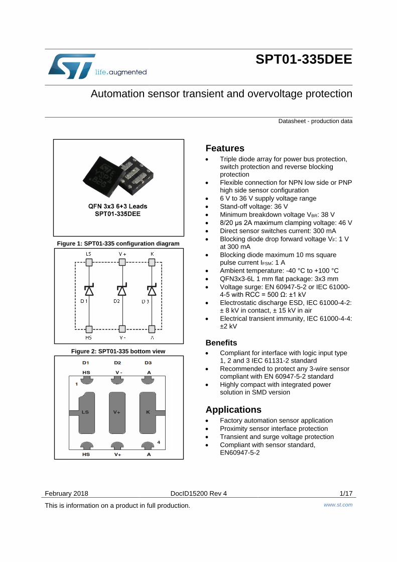
Figure 1: SPT01-335 configuration diagram
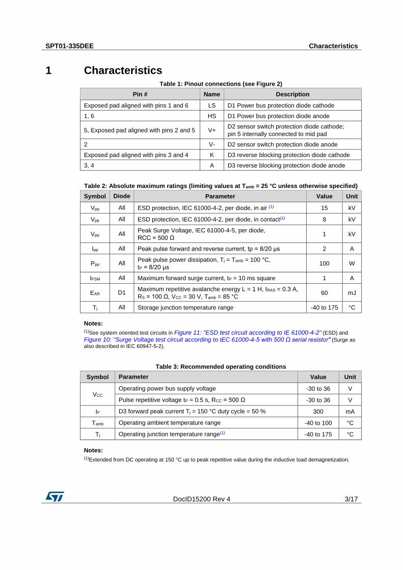
Figure 2: SPT01-335 bottom view
Features Triple diode array for power bus protection,
switch protection and reverse blocking protection
Flexible connection for NPN low side or PNP high side sensor configuration
6 V to 36 V supply voltage range
Stand-off voltage: 36 V
Minimum breakdown voltage VBR: 38 V
8/20 μs 2A maximum clamping voltage: 46 V
Direct sensor switches current: 300 mA
Blocking diode drop forward voltage VF: 1 V at 300 mA
Blocking diode maximum 10 ms square pulse current IFSM: 1 A
Ambient temperature: -40 °C to +100 °C
QFN3x3-6L 1 mm flat package: 3x3 mm
Voltage surge: EN 60947-5-2 or IEC 61000-4-5 with RCC = 500 Ω: ±1 kV
Electrostatic discharge ESD, IEC 61000-4-2: ± 8 kV in contact, ± 15 kV in air
This is information on a product in full production. www.st.com
Description The SPT01-335 is specifically designed for the protection of 24 V proximity sensors. It implements the reverse polarity and the overvoltage protection of the sensor power supply and the power switch overvoltage protection.
It provides a very compact and flexible solution offering two connections for PNP or NPN sensors as shown in Figure 8: "PNP high side sensor configuration" and Figure 9.
Thanks to high performance ST technology, the SPT01-335 protects the proximity sensor to the highest level compliant with IEC 61000-4-2, IEC 61000-4-4 and IEC 60947-5-2 / IEC 61000-4-5 standards.
SPT01-335DEE Characteristics
DocID15200 Rev 4 3/17
1 Characteristics Table 1: Pinout connections (see Figure 2)
Pin # Name Description
Exposed pad aligned with pins 1 and 6 LS D1 Power bus protection diode cathode
1, 6 HS D1 Power bus protection diode anode
5, Exposed pad aligned with pins 2 and 5 V+ D2 sensor switch protection diode cathode;
pin 5 internally connected to mid pad
2 V- D2 sensor switch protection diode anode
Exposed pad aligned with pins 3 and 4 K D3 reverse blocking protection diode cathode
3, 4 A D3 reverse blocking protection diode anode
Table 2: Absolute maximum ratings (limiting values at Tamb = 25 °C unless otherwise specified)
Symbol Diode Parameter Value Unit
Vpp All ESD protection, IEC 61000-4-2, per diode, in air (1) 15 kV
Vpp All ESD protection, IEC 61000-4-2, per diode, in contact(1) 8 kV
Vpp All Peak Surge Voltage, IEC 61000-4-5, per diode,
RCC = 500 Ω 1 kV
Ipp All Peak pulse forward and reverse current, tp = 8/20 μs 2 A
Ppp All Peak pulse power dissipation, Tj = Tamb = 100 °C,
tP = 8/20 μs 100 W
IFSM All Maximum forward surge current, tP = 10 ms square 1 A
EAR D1 Maximum repetitive avalanche energy L = 1 H, IRAS = 0.3 A,
RS = 100 Ω, VCC = 30 V, Tamb = 85 °C 60 mJ
Tj All Storage junction temperature range -40 to 175 °C
Notes: (1)See system oriented test circuits in Figure 11: "ESD test circuit according to IE 61000-4-2" (ESD) and
Figure 10: "Surge Voltage test circuit according to IEC 61000-4-5 with 500 Ω serial resistor" (Surge as
also described in IEC 60947-5-2).
Table 3: Recommended operating conditions
Symbol Parameter Value Unit
VCC Operating power bus supply voltage -30 to 36 V
Pulse repetitive voltage tP = 0.5 s, RCC = 500 Ω -30 to 36 V
IF D3 forward peak current Tj = 150 °C duty cycle = 50 % 300 mA
Tamb Operating ambient temperature range -40 to 100 °C
Tj Operating junction temperature range(1) -40 to 175 °C
Notes: (1)Extended from DC operating at 150 °C up to peak repetitive value during the inductive load demagnetization.
VRM All Reverse stand off voltage(1) IR = 0.2 µA Min. 33 V
IR = 1 µA Min. 36 V
IRM All Leakage reverse current
VRM = 33 V Max. 0.2 µA
VRM = 33 V,
TJ = 150 °C Max. 1 µA
VBR All Reverse breakdown voltage IR = 1 mA Min. 38 V
Typ. 41.4 V
VCL All Peak clamping voltage IPP = 2 A,
tP = 8 /20 μs
Max. 46 V
Typ. 44 V
RD All
Typ. 0.5 Ω
αT All
Max. 10 10-4 /°C
VCL D1
IR = 0.3 A,
L = 1 H,
tP = 8 /20 μs,
VCC = 30 V
Max. 46 V
VF D3
IF = 300 mA Max. 1 V
Notes: (1)Reverse stand-off voltage is valid for ambient temperature within the operating temperature range.
Table 5: Thermal resistances
Symbol Parameter Value Unit
Rth(j-a) SMD thermal resistance junction to ambient, per diode FR4 board, copper
thickness = 35 μm, SCu = 0.85 mm² 330 °C/W
Zth(j-a) SMD thermal transient impedance junction to ambient, per diode tp = 15 ms, Tamb = 85 °C, SCu = 0.85 mm²
20 °C/W
SPT01-335DEE Characteristics
DocID15200 Rev 4 5/17
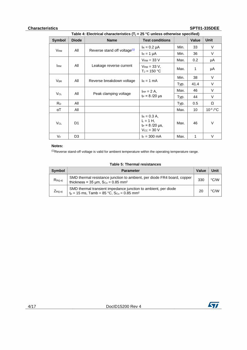
1.1 Characteristics (curves)
Figure 3: Relative variation of peak pulse power versus initial junction temperature
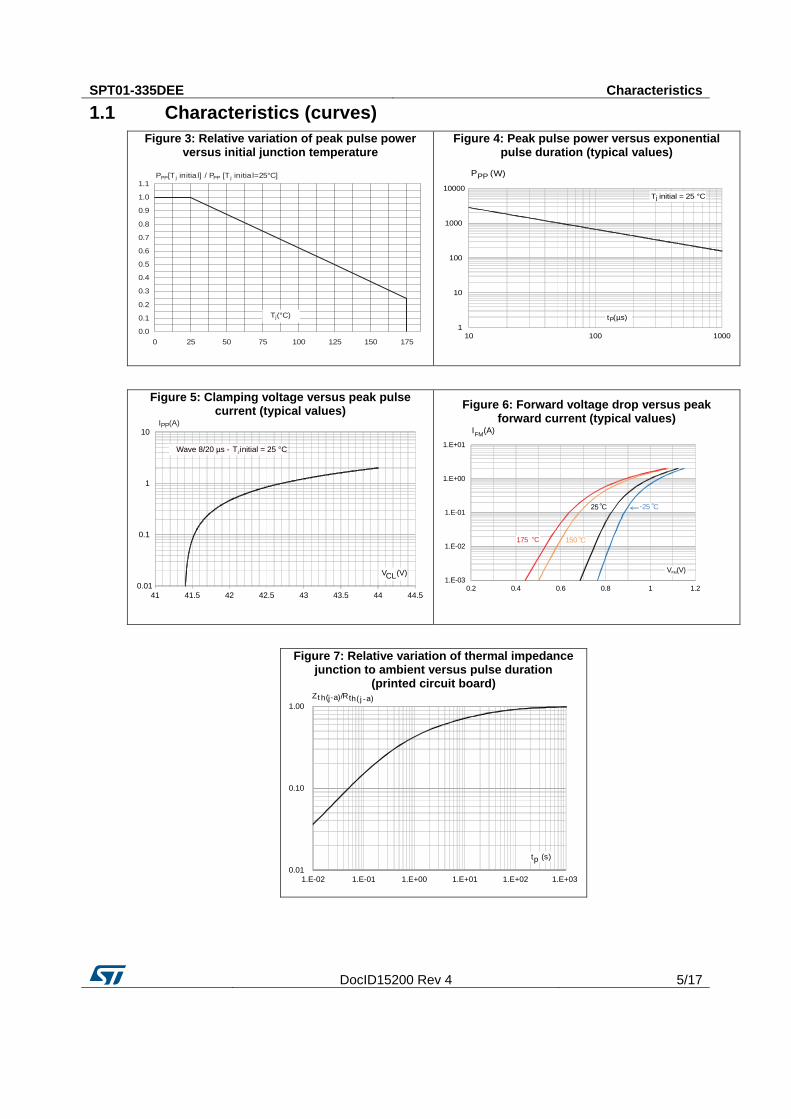
Figure 4: Peak pulse power versus exponential pulse duration (typical values)
Figure 5: Clamping voltage versus peak pulse current (typical values)
Figure 6: Forward voltage drop versus peak forward current (typical values)
Figure 7: Relative variation of thermal impedance junction to ambient versus pulse duration
(printed circuit board)
0.0
0.1
0.2
0.3
0.4
0.5
0.6
0.7
0.8
0.9
1.0
1.1
0 25 50 75 100 125 150 175
PPP[T j initia l] / PPP [T j initia l=25°C]
Tj(°C)
P (W)PP
1
10
100
1000
10000
10 100 1000
t (µs)P
Tj initial = 25 °C
I (A)PP
0.01
0.1
1
10
41 41.5 42 42.5 43 43.5 44 44.5
VCL(V)
Wave 8/20 µs - T initial = 25 °CJ
I (A)FM
1.E-03
1.E-02
1.E-01
1.E+00
1.E+01
0.2 0.4 0.6 0.8 1 1.2
175 °C 150°C
25°C -25 °C
V (V)FM
Zt h(j-a)/Rth( j -a)
0.01
0.10
1.00
1.E-02 1.E-01 1.E+00 1.E+01 1.E+02 1.E+03
tp (s)
SPT01-335DEE basic application SPT01-335DEE
6/17 DocID15200 Rev 4
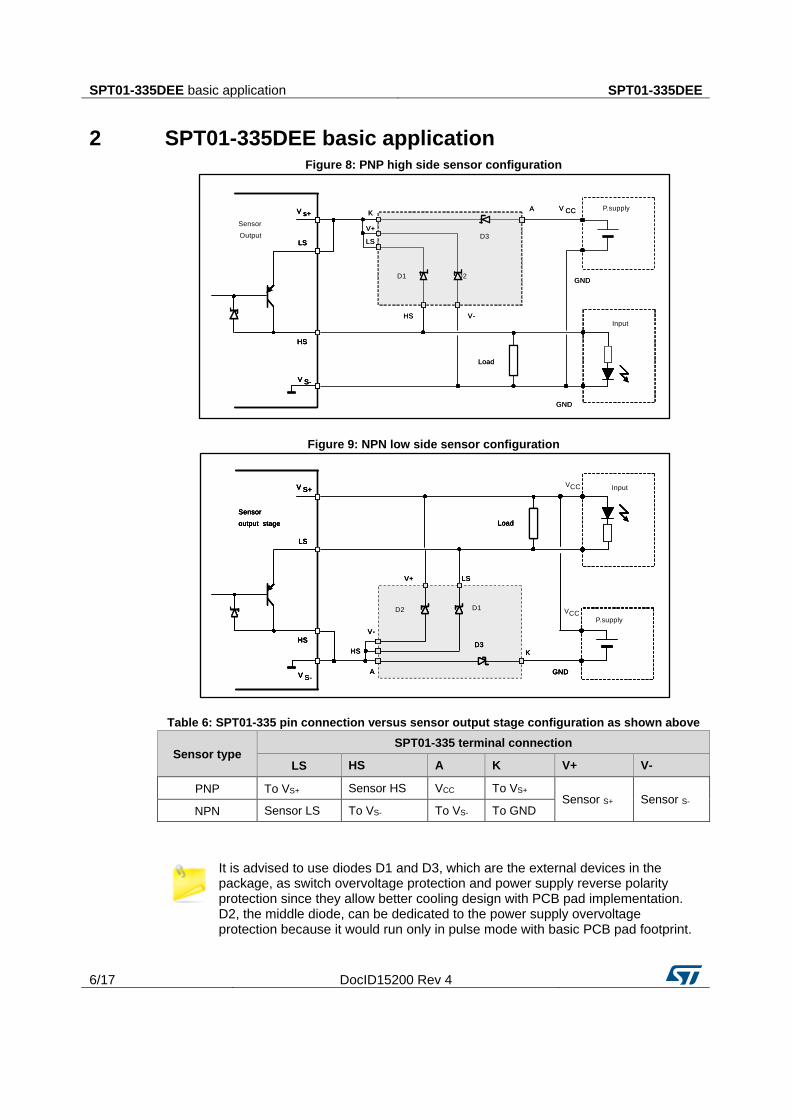
2 SPT01-335DEE basic application Figure 8: PNP high side sensor configuration
Figure 9: NPN low side sensor configuration
Table 6: SPT01-335 pin connection versus sensor output stage configuration as shown above
Sensor type SPT01-335 terminal connection
LS HS A K V+ V-
PNP To VS+ Sensor HS VCC To VS+ Sensor S+ Sensor S-
NPN Sensor LS To VS- To VS- To GND
It is advised to use diodes D1 and D3, which are the external devices in the package, as switch overvoltage protection and power supply reverse polarity protection since they allow better cooling design with PCB pad implementation. D2, the middle diode, can be dedicated to the power supply overvoltage protection because it would run only in pulse mode with basic PCB pad footprint.
V CC
GND
GND
Input
Load
V s+
LS
HS
V S-
Sensor
Output
A
V+D3
D1 D2
V-HS
K
LS
V CC
GND
GND
Load
V s+
LS
HS
V S-
V s+
LS
HS
V S-
V s+
LS
HS
V S-
A
V+D3
D1 D2
V-HS
K
LS
P.supply
LS
HS
V S-
V S+
Sensor
output stage
GND
Load
P.supply
Input
LS
D3
D2
V+
V-
KHS
A
LS
HS
V S-
V S+
Sensor
output stage
LS
HS
V S-
V S+
Sensor
output stage
LS
HS
V
V S+
LS
HS
V
V S+
Sensor
output stage
GND
Load
GND
Load
GND
Load
LS
D3
V+
V-
KHS
A
LS
D3
D1
V+
V-
KHS
A
VCC
VCC
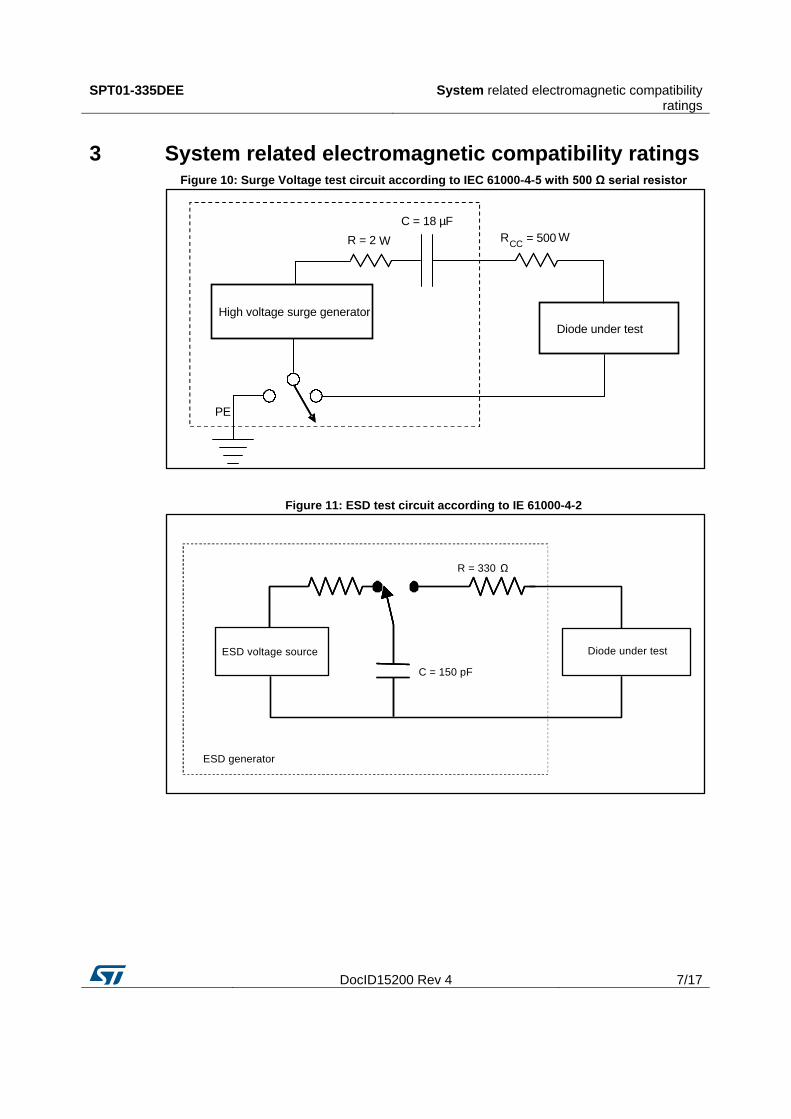
SPT01-335DEE System related electromagnetic compatibility ratings
DocID15200 Rev 4 7/17
3 System related electromagnetic compatibility ratings Figure 10: Surge Voltage test circuit according to IEC 61000-4-5 with 500 Ω serial resistor
Figure 11: ESD test circuit according to IE 61000-4-2
Diode under test
R = 2
C = 18 µF
PE
= 500W
High voltage surge generator
RCC
W
ESD voltage source
ESD generator
Diode under test
R = 330
C = 150 pF
Ω
Evaluation of the clamping voltage SPT01-335DEE
8/17 DocID15200 Rev 4
4 Evaluation of the clamping voltage VBR (TJ) = VBR (25) x (1+ αT (TJ – 25))
VCL MAX (8/20 μs) = VBR MAX + RD x IPP
4.1 Application considerations
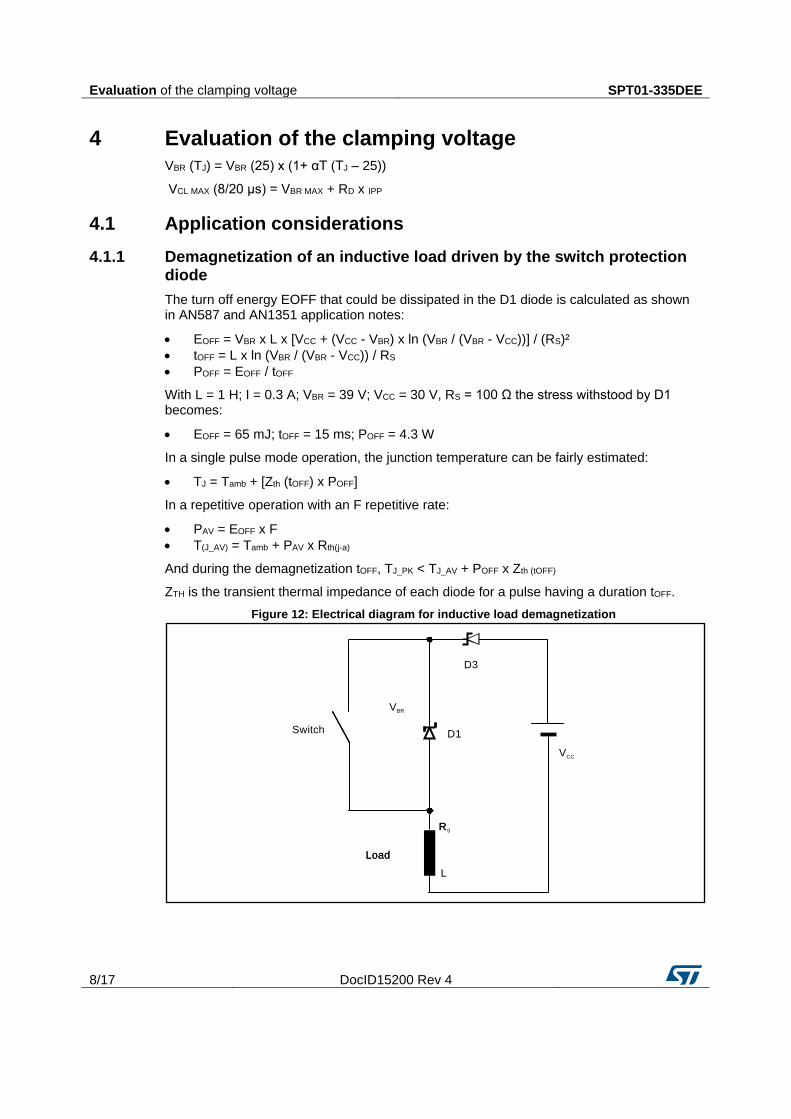
4.1.1 Demagnetization of an inductive load driven by the switch protection diode
The turn off energy EOFF that could be dissipated in the D1 diode is calculated as shown in AN587 and AN1351 application notes:
EOFF = VBR x L x [VCC + (VCC - VBR) x ln (VBR / (VBR - VCC))] / (RS)²
tOFF = L x ln (VBR / (VBR - VCC)) / RS
POFF = EOFF / tOFF
With L = 1 H; I = 0.3 A; VBR = 39 V; VCC = 30 V, RS = 100 Ω the stress withstood by D1 becomes:
EOFF = 65 mJ; tOFF = 15 ms; POFF = 4.3 W
In a single pulse mode operation, the junction temperature can be fairly estimated:
TJ = Tamb + [Zth (tOFF) x POFF]
In a repetitive operation with an F repetitive rate:
PAV = EOFF x F
T(J_AV) = Tamb + PAV x Rth(j-a)
And during the demagnetization tOFF, TJ_PK < TJ_AV + POFF x Zth (tOFF)
ZTH is the transient thermal impedance of each diode for a pulse having a duration tOFF.
Figure 12: Electrical diagram for inductive load demagnetization
Load
D3
D1
VCC
VBR
R
L
Load
Switch
RS
SPT01-335DEE Evaluation of the clamping voltage
DocID15200 Rev 4 9/17
4.1.2 Life time considerations
Life time of the product is calculated to exceed 10 years. The key parameters to consider are the ambient temperature (Tamb < 100 °C), the power supply voltage (VCC < 30 V), and the current in the reverse blocking diode (IF = 0.1 A switching at 0.5 Hz with 50% duty cycle, the stand-by current being less than 1.5 mA).
For higher current or higher switching frequency operation, the life time should be calculated considering the peak and average junction temperature.
This junction temperature can be reduced by reducing the thermal resistance of the clamping diode, D1 normally. This can be done by increasing its PCB copper tab surface SCu.
Package information SPT01-335DEE
10/17 DocID15200 Rev 4
5 Package information In order to meet environmental requirements, ST offers these devices in different grades of ECOPACK® packages, depending on their level of environmental compliance. ECOPACK® specifications, grade definitions and product status are available at: www.st.com. ECOPACK® is an ST trademark.
Epoxy meets UL94,V0
Lead-free package
5.1 QFN 3x3 package information
Figure 13: QFN 3x3 package outline
Index area
Top view
Bottom view
Side view
Pin#1 ID
D
A1A
E
e
b1
b
E2
L1D2
L
k1
K
3
4
1
6
SPT01-335DEE Package information
DocID15200 Rev 4 11/17
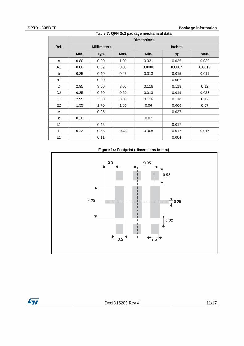
Table 7: QFN 3x3 package mechanical data
Ref.
Dimensions
Millimeters Inches
Min. Typ. Max. Min. Typ. Max.
A 0.80 0.90 1.00 0.031 0.035 0.039
A1 0.00 0.02 0.05 0.0000 0.0007 0.0019
b 0.35 0.40 0.45 0.013 0.015 0.017
b1
0.20
0.007
D 2.95 3.00 3.05 0.116 0.118 0.12
D2 0.35 0.50 0.60 0.013 0.019 0.023
E 2.95 3.00 3.05 0.116 0.118 0.12
E2 1.55 1.70 1.80 0.06 0.066 0.07
e
0.95
0.037
k 0.20
0.07
k1
0.45
0.017
L 0.22 0.33 0.43 0.008 0.012 0.016
L1
0.11
0.004
Figure 14: Footprint (dimensions in mm)
Package information SPT01-335DEE
12/17 DocID15200 Rev 4
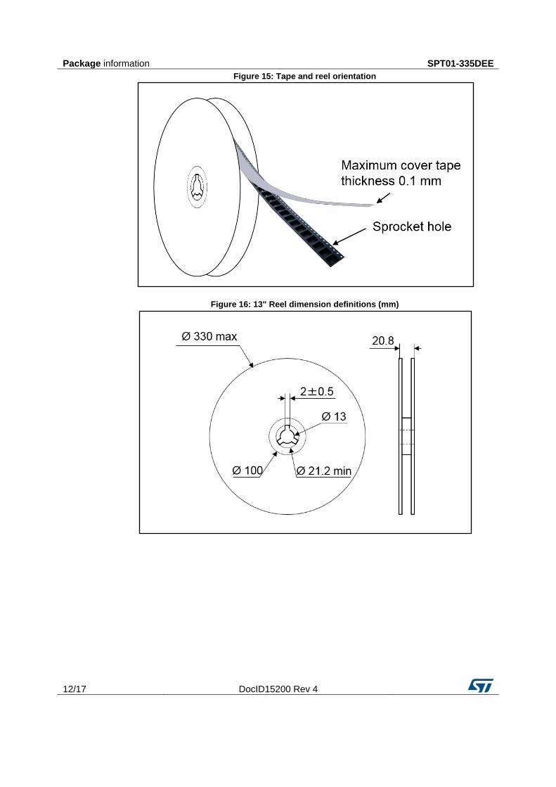
Figure 15: Tape and reel orientation
Figure 16: 13" Reel dimension definitions (mm)
SPT01-335DEE Package information
DocID15200 Rev 4 13/17
Figure 17: Tape and reel outline
Table 8: Tape and reel mechanical data
Ref.
Dimensions
Millimeters
Min. Typ. Max.
P1 7.9 8.0 8.1
P0 3.9 4.0 4.1
ØD0 1.5 1.5 1.6
ØD1 1.5
F 5.45 5.5 5.55
K0
1.1
P2 1.95 2.0 2.05
W 11.7 12 12.3
A0 3.3
B0 3.3
Recommendation on PCB assembly SPT01-335DEE
14/17 DocID15200 Rev 4
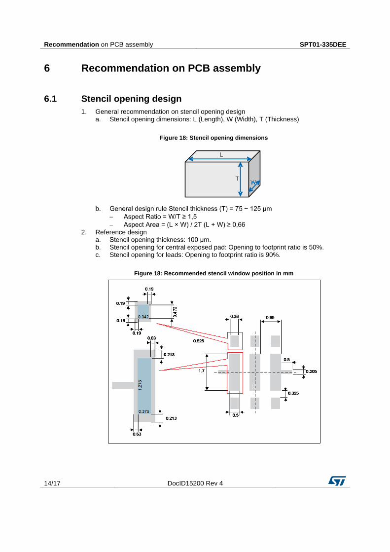
6 Recommendation on PCB assembly
6.1 Stencil opening design
1. General recommendation on stencil opening design a. Stencil opening dimensions: L (Length), W (Width), T (Thickness)
Figure 18: Stencil opening dimensions
b. General design rule Stencil thickness (T) = 75 ~ 125 μm
a. Stencil opening thickness: 100 μm. b. Stencil opening for central exposed pad: Opening to footprint ratio is 50%. c. Stencil opening for leads: Opening to footprint ratio is 90%.
Figure 18: Recommended stencil window position in mm
SPT01-335DEE Recommendation on PCB assembly
DocID15200 Rev 4 15/17
6.2 Solder paste
1. Halide-free flux qualification ROL0 according to ANSI/J-STD-004. 2. “No clean” solder paste is recommended. 3. Offers a high tack force to resist component movement during high speed. 4. Use solder paste with fine particles: powder particle size 20-45 µm.
6.3 Placement
1. Manual positioning is not recommended. 2. It is recommended to use the lead recognition capabilities of the placement system,
not the outline centering 3. Standard tolerance of ±0.05 mm is recommended. 4. 3.5 N placement force is recommended. Too much placement force can lead to
squeezed out solder paste and cause solder joints to short. Too low placement force can lead to insufficient contact between package and solder paste that could cause open solder joints or badly centered packages.
5. To improve the package placement accuracy, a bottom side optical control should be performed with a high resolution tool.
6. For assembly, a perfect supporting of the PCB (all the more on flexible PCB) is recommended during solder paste printing, pick and place and reflow soldering by using optimized tools.
6.4 PCB design preference
1. To control the solder paste amount, the closed via is recommended instead of open vias.
2. The position of tracks and open vias in the solder area should be well balanced. A symmetrical layout is recommended, to avoid any tilt phenomena caused by asymmetrical solder paste due to solder flow away.
6.5 Reflow profile
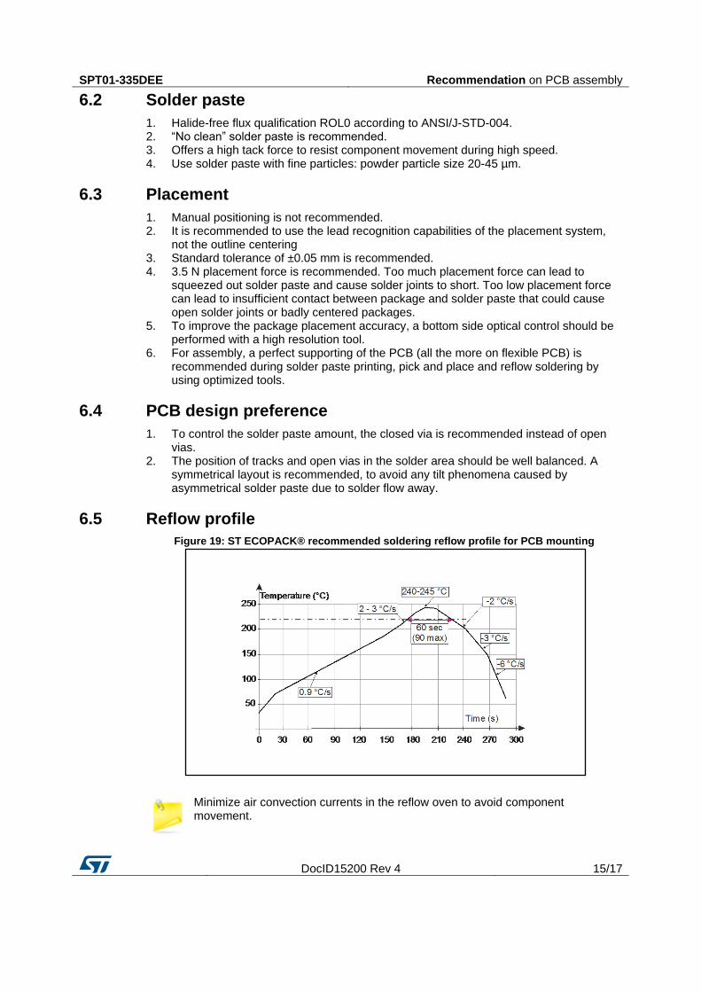
Figure 19: ST ECOPACK® recommended soldering reflow profile for PCB mounting
Minimize air convection currents in the reflow oven to avoid component movement.
Ordering information SPT01-335DEE
16/17 DocID15200 Rev 4
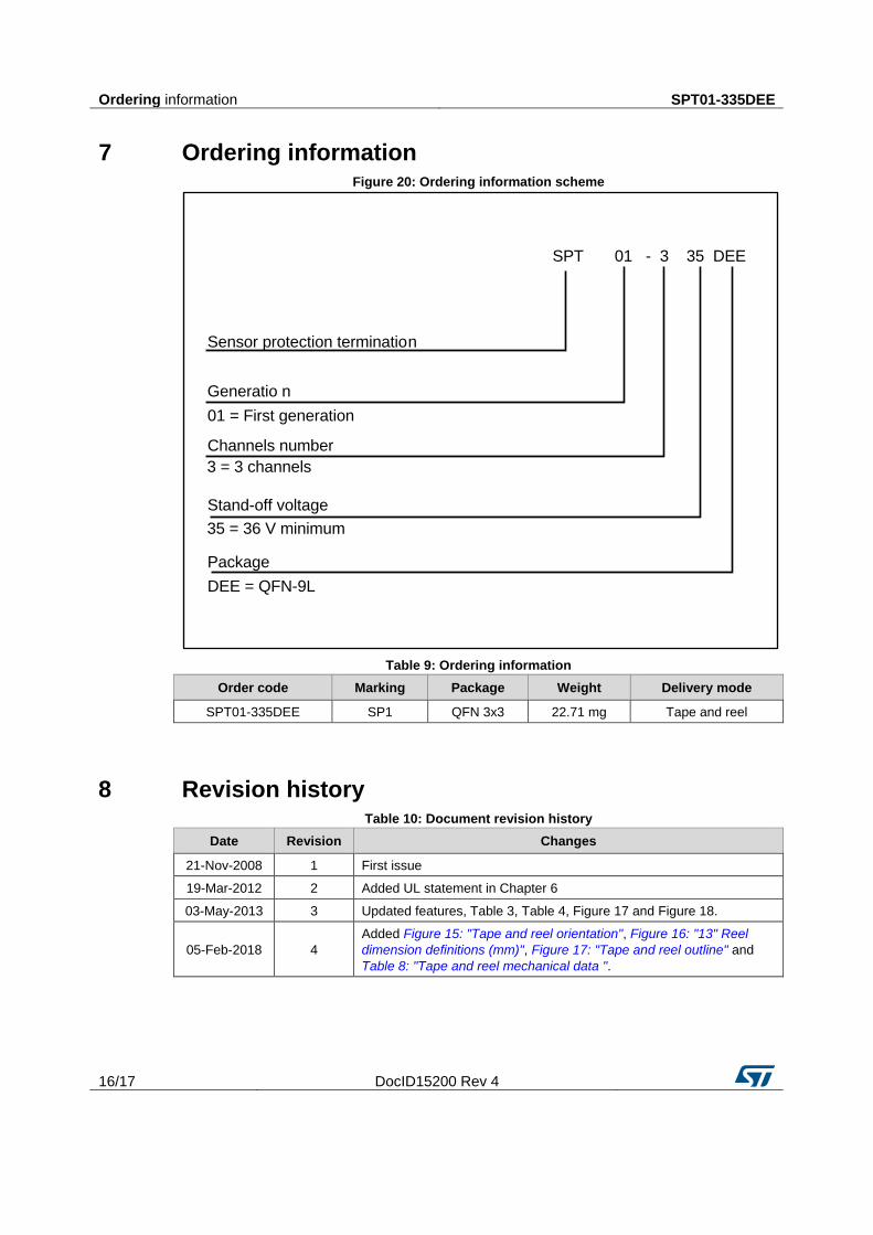
7 Ordering information Figure 20: Ordering information scheme
Table 9: Ordering information
Order code Marking Package Weight Delivery mode
SPT01-335DEE SP1 QFN 3x3 22.71 mg Tape and reel
8 Revision history Table 10: Document revision history
dimension definitions (mm)", Figure 17: "Tape and reel outline" and
Table 8: "Tape and reel mechanical data ".
SPT 01 - 3 35 DEE
Sensor protection termination
Generatio n
01 = First generation
Channels number
3 = 3 channels
35 = 36 V minimum
Package
DEE = QFN-9L
Stand-off voltage
SPT01-335DEE
DocID15200 Rev 4 17/17
9 Disclaimer
IMPORTANT NOTICE – PLEASE READ CAREFULLY
STMicroelectronics NV and its subsidiaries (“ST”) reserve the right to make changes, corrections, enhancements, modifications , and improvements to ST products and/or to this document at any time without notice. Purchasers should obtain the latest relevant information on ST products before placing orders. ST products are sold pursuant to ST’s terms and conditions of sale in place at the time of order acknowledgement.
Purchasers are solely responsible for the choice, selection, and use of ST products and ST assumes no liability for application assistance or the design of Purchasers’ products.
No license, express or implied, to any intellectual property right is granted by ST herein.
Resale of ST products with provisions different from the information set forth herein shall void any warranty granted by ST for such product.
ST and the ST logo are trademarks of ST. All other product or service names are the property of their respective owners.
Information in this document supersedes and replaces information previously supplied in any prior versions of this document.