This is information on a product in full production. February 2015 DocID13208 Rev 5 1/15 STB270N4F3 Automotive-grade N-channel 40 V, 1.6 mΩ typ., 160 A STripFET™ F3 Power MOSFET in a D 2 PAK package Datasheet - production data Figure 1. Internal schematic diagram Features • Designed for automotive applications and AEC-Q101 qualified • 100% avalanche tested • Standard threshold drive Applications • Switching application Description This device is an N-channel Power MOSFET developed using STripFET™ F3 technology. It is designed to minimize on-resistance and gate charge to provide superior switching performance. Type V DS R DS(on) max I D P TOT STB270N4F3 40 V 2.0 mΩ 160 A 330 W Table 1. Device summary Order codes Marking Package Packaging STB270N4F3 270N4F3 D²PAK Tape and reel www.st.com
Transcript
This is information on a product in full production.
February 2015 DocID13208 Rev 5 1/15
STB270N4F3
Automotive-grade N-channel 40 V, 1.6 mΩ typ., 160 A STripFET™ F3 Power MOSFET in a D2PAK package
Datasheet - production data
Figure 1. Internal schematic diagram
Features
• Designed for automotive applications and AEC-Q101 qualified
• 100% avalanche tested
• Standard threshold drive
Applications• Switching application
DescriptionThis device is an N-channel Power MOSFET developed using STripFET™ F3 technology. It is designed to minimize on-resistance and gate charge to provide superior switching performance.
Figure 13. Switching times test circuit for resistive load
Figure 14. Gate charge test circuit
Figure 15. Test circuit for inductive load switching and diode recovery times
Figure 16. Unclamped inductive load test circuit
Figure 17. Unclamped inductive waveform Figure 18. Switching time waveform
AM01468v1
VGS
PW
VD
RG
RL
D.U.T.
2200
μF3.3μF
VDD
AM01469v1
VDD
47kΩ 1kΩ
47kΩ
2.7kΩ
1kΩ
12V
Vi=20V=VGMAX
2200μF
PW
IG=CONST100Ω
100nF
D.U.T.
VG
AM01470v1
AD
D.U.T.
SB
G
25 Ω
A A
BB
RG
G
FASTDIODE
D
S
L=100μH
μF3.3 1000
μF VDD
AM01471v1
Vi
Pw
VD
ID
D.U.T.
L
2200μF
3.3μF VDD
AM01472v1
V(BR)DSS
VDDVDD
VD
IDM
ID
AM01473v1
VDS
ton
tdon tdoff
toff
tftr
90%
10%
10%
0
0
90%
90%
10%
VGS
DocID13208 Rev 5 9/15
STB270N4F3 Package information
15
4 Package information
In order to meet environmental requirements, ST offers these devices in different grades of ECOPACK® packages, depending on their level of environmental compliance. ECOPACK® specifications, grade definitions and product status are available at: www.st.com. ECOPACK is an ST trademark.
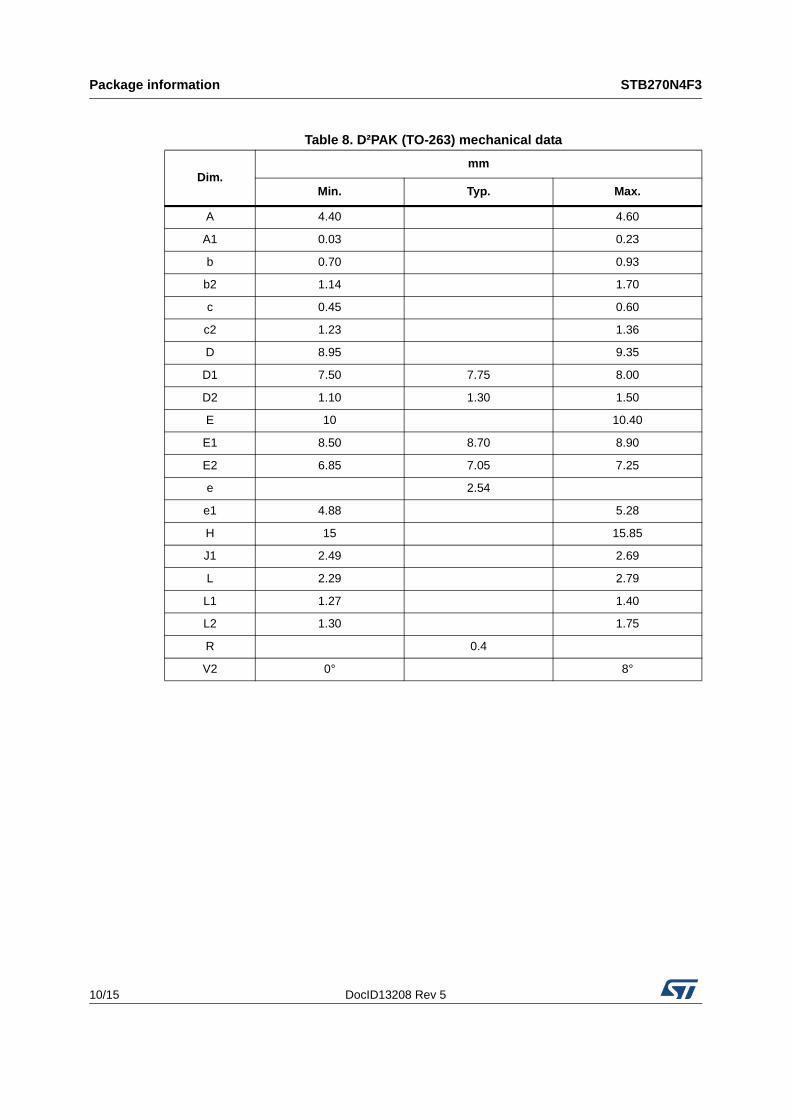
4.1 D2PAK package information
Figure 19. D²PAK (TO-263) outline
Package information STB270N4F3
10/15 DocID13208 Rev 5
Table 8. D²PAK (TO-263) mechanical data
Dim.mm
Min. Typ. Max.
A 4.40 4.60
A1 0.03 0.23
b 0.70 0.93
b2 1.14 1.70
c 0.45 0.60
c2 1.23 1.36
D 8.95 9.35
D1 7.50 7.75 8.00
D2 1.10 1.30 1.50
E 10 10.40
E1 8.50 8.70 8.90
E2 6.85 7.05 7.25
e 2.54
e1 4.88 5.28
H 15 15.85
J1 2.49 2.69
L 2.29 2.79
L1 1.27 1.40
L2 1.30 1.75
R 0.4
V2 0° 8°
DocID13208 Rev 5 11/15
STB270N4F3 Package information
15
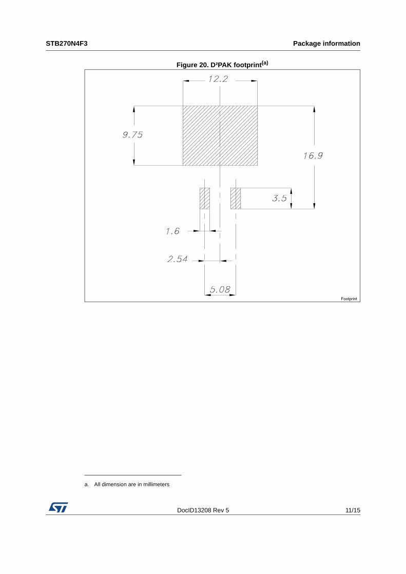
Figure 20. D²PAK footprint(a)
a. All dimension are in millimeters
Packing information STB270N4F3
12/15 DocID13208 Rev 5
5 Packing information
Figure 21. Tape
DocID13208 Rev 5 13/15
STB270N4F3 Packing information
15
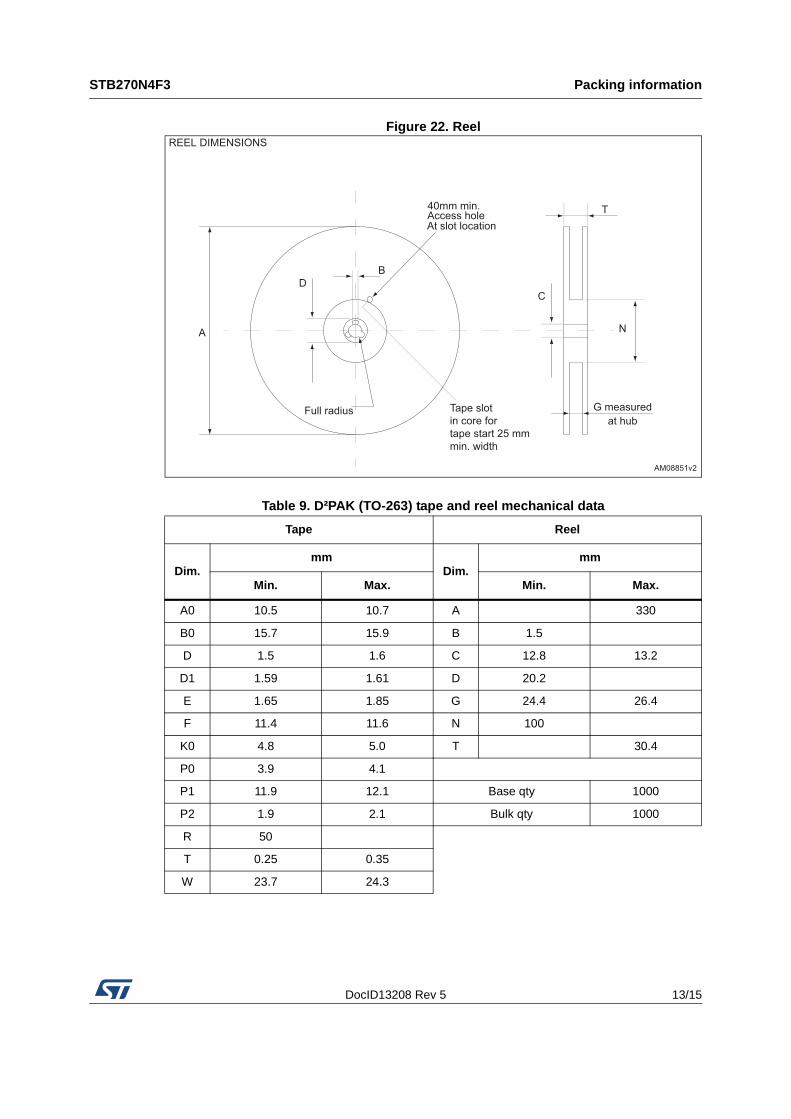
Figure 22. Reel
Table 9. D²PAK (TO-263) tape and reel mechanical data
Tape Reel
Dim.mm
Dim.mm
Min. Max. Min. Max.
A0 10.5 10.7 A 330
B0 15.7 15.9 B 1.5
D 1.5 1.6 C 12.8 13.2
D1 1.59 1.61 D 20.2
E 1.65 1.85 G 24.4 26.4
F 11.4 11.6 N 100
K0 4.8 5.0 T 30.4
P0 3.9 4.1
P1 11.9 12.1 Base qty 1000
P2 1.9 2.1 Bulk qty 1000
R 50
T 0.25 0.35
W 23.7 24.3
Revision history STB270N4F3
14/15 DocID13208 Rev 5
6 Revision history
Table 10. Revision history
Date Revision Changes
07-Feb-2007 1 Initial release.
02-Apr-2008 2 Some value changes onTable 2
06-May-2009 3Changed: Description and Figure 12: Source-drain diode forward characteristics
14-Jul-2009 4 Removed package and mechanical data: TO-220
26-Feb-2015 5
The part number STI270N4F3 has been moved to a separate document.Updated title, features and description cover page.
Updated Table 2: Absolute maximum ratings, Table 3: Thermal data.
Updated Section 4: Package information and Section 5: Packing information.
Minor text changes.
DocID13208 Rev 5 15/15
STB270N4F3
15
IMPORTANT NOTICE – PLEASE READ CAREFULLY
STMicroelectronics NV and its subsidiaries (“ST”) reserve the right to make changes, corrections, enhancements, modifications, and improvements to ST products and/or to this document at any time without notice. Purchasers should obtain the latest relevant information on ST products before placing orders. ST products are sold pursuant to ST’s terms and conditions of sale in place at the time of order acknowledgement.
Purchasers are solely responsible for the choice, selection, and use of ST products and ST assumes no liability for application assistance or the design of Purchasers’ products.
No license, express or implied, to any intellectual property right is granted by ST herein.
Resale of ST products with provisions different from the information set forth herein shall void any warranty granted by ST for such product.
ST and the ST logo are trademarks of ST. All other product or service names are the property of their respective owners.
Information in this document supersedes and replaces information previously supplied in any prior versions of this document.