Description The A6268 is a DC-to-DC converter controller, providing a programmable constant current output for driving high power LEDs in series. Driving the LEDs in series ensures identical currents and uniform brightness. For automotive applications, optimum performance is achieved when driving up to 15 LEDs at currents up to 1 A. The A6268 provides a cost-effective solution using an external logic-level MOSFET and minimum additional external components. The maximum LED current is set with a single external sense resistor and can be modified using a current reference input. Direct PWM control is possible via the Enable input, which also provides a shutdown mode. This DC-DC converter can be configured as a ground-referenced boost converter or as a supply-referenced boost converter providing buck-boost capability. The buck-boost topology used ensures that there is no leakage path through the LEDs when in shutdown and no inrush current at power-up. Integrated diagnostics and two fault outputs give indication of VIN and VREG undervoltage, chip overtemperature, output open circuit, LED short circuit and LED undercurrent, and can be configured to provide short to supply and short to ground protection for the LED connections, LED overcurrent and shorted LED string protection. A unique feature is the ability to detect one or more shorted LEDs. The device is provided in a 16-pin TSSOP package with exposed thermal pad (suffix LP). It is lead (Pb) free, with 100% matte tin leadframe plating. A6268-DS, Rev. 3 Features and Benefits ▪ AEC-Q100 Grade 0 Automotive Qualified ▪ Constant current LED drive ▪ 5 to 50 V supply ▪ Boost or buck-boost modes ▪ Drives up to 15 LEDs in series ▪ Programmable switching frequency 100 to 700 kHz ▪ Open LED overvoltage indication and protection ▪ Single and multiple LED short indication ▪ LED short to ground and supply protection ▪ PWM dimming control ▪ 10 μA shutdown current including LED leakage Automotive High Current LED Controller Package: 16-pin TSSOP with exposed thermal pad (suffix LP) Applications: Typical Application Diagrams Not to scale A6268 Buck-Boost Mode (Supply-referenced boost) Boost Mode ▪ Automotive high power LED lighting systems ▪ Fog lights, reversing lights, daytime running lights ▪ Headlights LN LP LF SG SP SN GND LA Fault Flags Power net VREG FF1 FF2 EN IREF CKOUT OSC Enable A6268 VIN V BAT 12 V or 24 V (50 V max) GND LA V BAT 12 V or 24 V (50 V max) LN LP LF SG SP SN Fault Flags Power net FF1 FF2 EN IREF CKOUT OSC Enable A6268 VREG VIN Boost Mode V BAT (min) (V) Maximum Quantity of LEDs 5 8 6 10 7 12 8 13 9 15 V f of each LED = 3.5 V, D(max) = 85% Buck Boost Mode V BAT (min) (V) Maximum Quantity of LEDs 5 7 6 8 7 10 8 11 9 13 V f of each LED = 3.5 V, D(max) = 85%
Transcript
DescriptionThe A6268 is a DC-to-DC converter controller, providing a programmable constant current output for driving high power LEDs in series. Driving the LEDs in series ensures identical currents and uniform brightness. For automotive applications, optimum performance is achieved when driving up to 15 LEDs at currents up to 1 A.
The A6268 provides a cost-effective solution using an external logic-level MOSFET and minimum additional external components. The maximum LED current is set with a single external sense resistor and can be modified using a current reference input. Direct PWM control is possible via the Enable input, which also provides a shutdown mode.
This DC-DC converter can be configured as a ground-referenced boost converter or as a supply-referenced boost converter providing buck-boost capability. The buck-boost topology used ensures that there is no leakage path through the LEDs when in shutdown and no inrush current at power-up.
Integrated diagnostics and two fault outputs give indication of VIN and VREG undervoltage, chip overtemperature, output open circuit, LED short circuit and LED undercurrent, and can be configured to provide short to supply and short to ground protection for the LED connections, LED overcurrent and shorted LED string protection. A unique feature is the ability to detect one or more shorted LEDs.
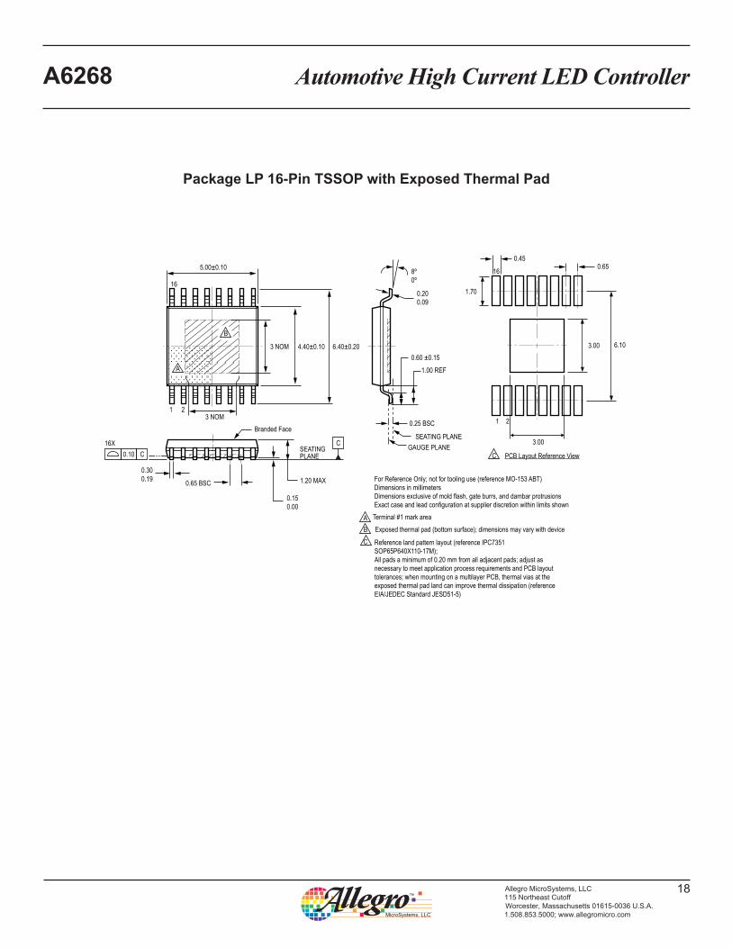
The device is provided in a 16-pin TSSOP package with exposed thermal pad (suffix LP). It is lead (Pb) free, with 100% matte tin leadframe plating.
A6268-DS, Rev. 3
Features and BenefitsAEC-Q100Grade0AutomotiveQualifiedConstantcurrentLEDdrive5to50VsupplyBoostorbuck-boostmodesDrivesupto15LEDsinseriesProgrammableswitchingfrequency100to700kHzOpenLEDovervoltageindicationandprotectionSingleandmultipleLEDshortindicationLEDshorttogroundandsupplyprotectionPWMdimmingcontrol10μAshutdowncurrentincludingLEDleakage
Automotive High Current LED Controller
Package: 16-pin TSSOP with exposed thermal pad (suffix LP)
Enable Input Internal Clamp Voltage VENC – 8.4 – V
Enable Input Current Limit Resistor REN Between EN and internal clamp – 200 – kΩ
Boost Mode Select Voltage VLNB Defined by VLN – – 0.8 V
Buck-Boost Mode Select Voltage VLNBB Defined by VLN 3.5 – – V
Disable Time tDIS fOSC = 350 kHz – 94 – ms
ELECTRICAL CHARACTERISTICS1 Valid at TJ = –40°C to 150°C, VIN = 5 to 40 V; unless otherwise notedCharacteristics Symbol Test Conditions Min. Typ. Max. Unit
ELECTRICAL CHARACTERISTICS1 (continued) Valid at TJ = –40°C to 150°C, VIN = 5 to 40 V; unless otherwise notedCharacteristics Symbol Test Conditions Min. Typ. Max. Unit
ELECTRICAL CHARACTERISTICS1 (continued) Valid at TJ = –40°C to 150°C, VIN = 5 to 40 V; unless otherwise notedCharacteristics Symbol Test Conditions Min. Typ. Max. Unit
Diagnostics and Protection (continued)LED String Short Voltage VSCL 350 475 600 mV
Non-Reference LED Short Offset Voltage VSCO 150 225 300 mV
Reference LED Short Offset Voltage VSCOR 350 475 600 mV
LED Open Voltage VOCL 5 5.5 6 V
LF Bias Current (BB mode)3 ILF LF = LA = VIN + 1.7 V – 50 – μA
LA Bias Current (BB mode)3 ILA LF = LA = VIN + 1.7 V – 90 – μA
LF Bias Current (B mode)3 ILF LF = 1.7 V – 8 – μA
LA Bias Current (B mode)3 ILA LA = 1.7 V – 24 – μA
LED Undercurrent Voltage Difference6 VUCL – 1 – mV
LED Overcurrent Voltage Difference7 VOVCL – 1 – mV
LED Sense Resistor Negative Overcurrent Threshold8 VNOCL VNOCL = VLP – VLN – –200 – mV
Open Fault Time-Out tOTO fOSC = 350 kHz – 94 – ms
Overtemperature Shutdown Threshold TJF Temperature increasing – 170 – ºC
Overtemperature Hysteresis TJhys Recovery = TJF – TJhys – 15 – ºC1For input and output current specifications, negative current is defined as coming out of (sourcing) the specified device pin.2Function is correct but parameters are not guaranteed below the general limit (5 V).3Parameters ensured by design.4BB mode = buck-boost (supply-referenced) mode, B mode = boost (ground-referenced) mode.5Fault Blank timer not enabled for open-LED condition.6Undercurrent when VSENSEL < VIDL– VUCL , where VSENSEL is the voltage across the LED current sense resistor RSL.7Overcurrent when VSENSEL > VIDL+VOVCL , where VSENSEL is the voltage across the LED current sense resistor RSL.8Protection only provided in buck-boost mode with LED cathode (LP) connection shorted to ground.
Functional DescriptionThe A6268 is a DC-DC converter controller that is designed to drive series-connected high power LEDs in automotive applica-tions. It provides programmable constant current output at load voltages and currents limited only by the external components. For automotive applications optimum performance is achieved when driving up to 15 LEDs at currents up to 1 A.
The A6268 can be configured as a standard boost converter or as a supply referenced boost converter. In the supply referenced configuration the load voltage is the difference between the boost voltage and the supply voltage. This difference can be greater than, equal to, or less than the supply voltage, effectively provid-ing a buck-boost capability. This configuration provides seam-less, uninterrupted operation over the wide supply voltage range possible in automotive applications and, because the output is ref-erenced to the positive supply, there is no load current to ground. This ensures that there is no leakage path through the LEDs when in shutdown and no inrush current at power-up.
The A6268 integrates all necessary control elements to pro-vide a cost-effective solution using a single external logic-level MOSFET and minimum additional external passive components.
The LED current is set by selecting an appropriate value for the sense resistor value and using the EN input to provide simple on-off control or for PWM brightness control using a suitable externally generated PWM signal. The LED current can be reduced in a single step by reducing the voltage between the IREF pin and GND to less than 1 V.
The pin functions and circuit operation are described in detail in the following sections.
Pin FunctionsVIN Supply to the control circuit. A bypass capacitor must be connected between this pin and GND.
GND Ground reference connection. This pin should be connected directly to the negative supply.
EN Logic input to enable operation. Can be used as direct PWM input. Chip enters low power sleep mode when low for longer than the disable time, tDIS.
FF1 Fault Flag output and isolation control. Open drain current sink output, when high impedance indicates detection of a critical circuit fault. An external pull-up resistor should be connected to a suitable logic supply for simple logic fault flag operation or to the
source of the PMOS FET used to isolate the load from the supply. Table 1 defines when FF1 is active. If FF1 is pulled low when an output short fault is indicated then the output disable will be overridden.
FF2 Fault Flag output. Open drain output, when high impedance indicates detection of a circuit fault. An external pull-up resistor should be connected to a suitable logic supply. If VREG is not used, then the logic supply should not be pulled 300 mV above VREG. Table 1 defines when FF2 is active. If FF2 is pulled low when an open LED fault is indicated then the output disable will be overridden.
OSC Resistor to ground to set the internal oscillator or clock input from external oscillator. When connected to VREG or GND theoscillatorrunsattypically350kHz.Higheraccuracyinthefrequency is possible by connecting a resistor from this pin to ground or by driving this pin with an external precision oscillator.
CKOUT Logic output at the oscillator frequency with phase shift. Used to drive succeeding controllers to interleave switching instants.
IREF LED current reference modifier. A voltage input that can be used to reduce the LED current sense voltage. When connected to VREG, the current sense voltage, VIDL, and the value of the sense resistor, RSL , define the maximum LED current.
SG Gate drive for external logic-level MOSFET low-side switch that connects the inductor to ground.
SP, SN Sense amplifier connections for switch current limit sense resistor, RSS .
LP Positive sense amplifier connection for LED current limit sense resistor, RSL .
LN Negative sense amplifier connection for LED current limit sense resistor, RSL . The voltage at LN also determines whether the boost or buck-boost mode is configured.
VREG Compensation capacitor for internal 5 V regulator.
LA Anode reference connection to LEDs. Using an external resis-tor divider with the same ratio as the number of LEDs provides a measurement of the voltage across all LEDs in the load. This is compared to the voltage on the LF pin to provide shorted LED detection. In addition, it is compared against voltage references to provide open circuit or shorted LED string detection.
LF Single diode forward voltage reference input. Measures the forward voltage of the first LED. This value is used as a reference against the voltage on the LA pin to detect possible shorted LEDs in the LED string.
Circuit OperationConverter A constant frequency, current mode control scheme is used to regulate the current through the LEDs. There are two control loops within the regulator. The inner loop formed by the amplifier,AS(seetheFunctionalBlockDiagramforAS,AC,AE,and AL), comparator, AC, and the RS bistable, controls the induc-tor current as measured through the switch by the switch sense resistor, RSS .
The outer loop including the amplifier, AL, and the integrating error amplifier, AE, controls the average LED current by provid-ing a setpoint reference for the inner loop.
The LED current is measured by the LED sense resistor, RSL , and compared to the internal reference current to produce an integrated error signal at the output of AE. This error signal sets the average amount of energy required from the inductor by the LEDs. The average inductor energy transferred to the LEDs is defined by the average inductor current as determined by the inner control loop.
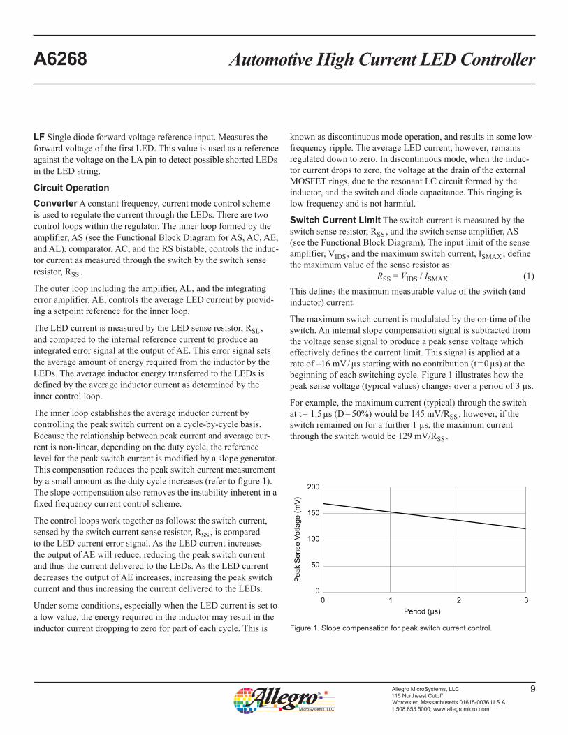
The inner loop establishes the average inductor current by controlling the peak switch current on a cycle-by-cycle basis. Becausetherelationshipbetweenpeakcurrentandaveragecur-rent is non-linear, depending on the duty cycle, the reference level for the peak switch current is modified by a slope generator. This compensation reduces the peak switch current measurement by a small amount as the duty cycle increases (refer to figure 1). The slope compensation also removes the instability inherent in a fixed frequency current control scheme.
The control loops work together as follows: the switch current, sensed by the switch current sense resistor, RSS , is compared to the LED current error signal. As the LED current increases the output of AE will reduce, reducing the peak switch current and thus the current delivered to the LEDs. As the LED current decreases the output of AE increases, increasing the peak switch current and thus increasing the current delivered to the LEDs.
Under some conditions, especially when the LED current is set to a low value, the energy required in the inductor may result in the inductorcurrentdroppingtozeroforpartofeachcycle.Thisis
known as discontinuous mode operation, and results in some low frequency ripple. The average LED current, however, remains regulateddowntozero.Indiscontinuousmode,whentheinduc-torcurrentdropstozero,thevoltageatthedrainoftheexternalMOSFET rings, due to the resonant LC circuit formed by the inductor, and the switch and diode capacitance. This ringing is low frequency and is not harmful.
Switch Current Limit The switch current is measured by the switch sense resistor, RSS , and the switch sense amplifier, AS (seetheFunctionalBlockDiagram).Theinputlimitofthesenseamplifier, VIDS , and the maximum switch current, ISMAX , define the maximum value of the sense resistor as: RSS = VIDS / ISMAX (1)
This defines the maximum measurable value of the switch (and inductor) current.
The maximum switch current is modulated by the on-time of the switch. An internal slope compensation signal is subtracted from the voltage sense signal to produce a peak sense voltage which effectively defines the current limit. This signal is applied at a rate of –16 mV / µs starting with no contribution (t = 0 µs) at the beginning of each switching cycle. Figure 1 illustrates how the peak sense voltage (typical values) changes over a period of 3 µs.
For example, the maximum current (typical) through the switch at t = 1.5 µs (D = 50%) would be 145 mV/RSS , however, if the switch remained on for a further 1 µs, the maximum current through the switch would be 129 mV/RSS .
200
150
100
50
00 1
Period (µs)
Pea
k S
ense
Vot
lage
(mV
)
2 3
Figure 1. Slope compensation for peak switch current control.
LED Current Level The LED current is determined by a combination of the LED sense resistor, RSL , the LED current threshold voltage, VIDL , and the voltage between the IREF pin and GND ( VIREF ).
The 100% current level, when the IREF pin is connected to VREG, is defined as: ILED(max) = VIDL / RSL (2)
If VIREF is less than 1 V then the 100% current level is defined as:
ILED(max) = VIREF / (10 × RSL ) (3)
This feature provides direct analog dimming using a voltage from 0 to 1 V. This can be used for a number of different functions:
• To provide intensity matching between modules or groups of LEDs in critical display or backlighting applications.
• To provide a soft start, by connecting a capacitor from IREF to GND and a resistor from IREF to VREG, or one-step dimming by use of a single logic control.
• To reduce the LED current during cold-crank conditions, thus avoiding overstressing the power components
LED Brightness: PWM Dimming LED brightness can be controlled by changing the current, which affects the light intensity.Howeverinsomeapplications,forexamplewithamberLEDs, this will have some effect on the color of the LEDs. In these cases it is more desirable to control the brightness by switching the fixed LED current with a pulse width modulated signal. This allows the LED brightness to be set with little effect on the LED color and intensity and allows direct digital control of the LED brightness.
A PWM signal can be applied to the EN input to enable PWM dimming. The period of this signal should be less than the minimum disable time, tDIS . During PWM dimming, the A6268 switches the LED current between 100% and 0% of the full cur-rent. Note that during PWM dimming, the gate drive is disabled when EN is low. The rate of change of the LED current is also limited, to reduce any large variations in the input current.
Sleep Mode If EN is held low for longer than the disable time, tDIS , then the A6268 will shut down and put all sections into a low-power sleep mode. In this mode the bias current is typically less than 4 µA. In the buck-boost configuration the only leakage path remaining will be the path through the MOSFET.
Provided this is low, then the complete circuit may remain con-nected to the power supply under all conditions. Note that the disable time is derived from the oscillator period by a ratio of 32,768:1,soanyvariationintheoscillatorfrequencywillchangethedisabletime.Forthedefaultswitchingfrequencyof350kHz,this means the disable time would be:
tDIS=32,768×(1/350×103 ) = 94 ms (4)
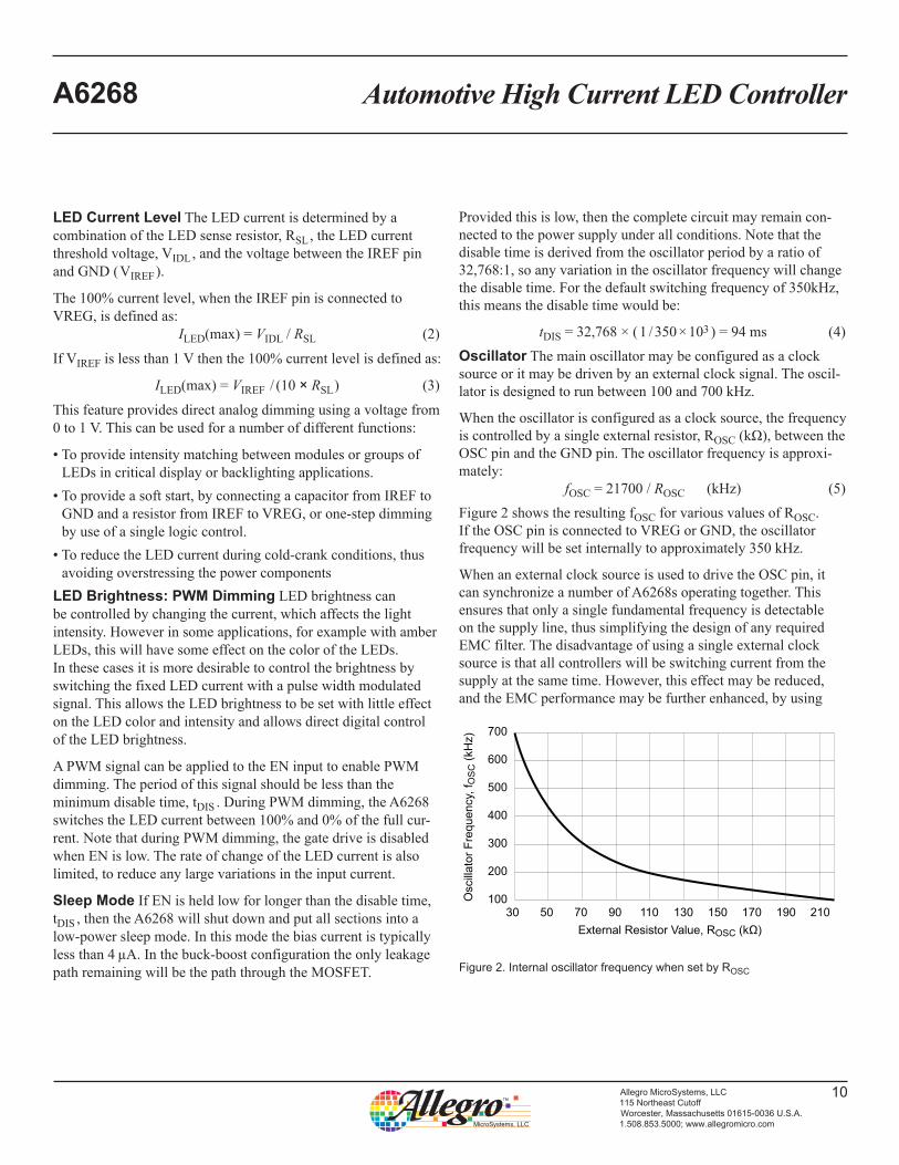
Oscillator The main oscillator may be configured as a clock source or it may be driven by an external clock signal. The oscil-latorisdesignedtorunbetween100and700kHz.
When the oscillator is configured as a clock source, the frequency is controlled by a single external resistor, ROSC(kΩ),betweentheOSC pin and the GND pin. The oscillator frequency is approxi-mately: fOSC=21700/ROSC(kHz) (5)
Figure 2 shows the resulting fOSC for various values of ROSC.If the OSC pin is connected to VREG or GND, the oscillator frequencywillbesetinternallytoapproximately350kHz.
When an external clock source is used to drive the OSC pin, it cansynchronizeanumberofA6268soperatingtogether.Thisensures that only a single fundamental frequency is detectable on the supply line, thus simplifying the design of any required EMC filter. The disadvantage of using a single external clock source is that all controllers will be switching current from the supplyatthesametime.However,thiseffectmaybereduced,and the EMC performance may be further enhanced, by using
700
600
500
400
300
200
10030 50 70 11090 130 150 170 190 210
External Resistor Value, ROSC (kΩ)
Osc
illat
or F
requ
ency
, fO
SC
(kH
z)
Figure 2. Internal oscillator frequency when set by ROSC
the CKOUT pin of another A6268 as the external clock source. In this case the switching point of each subsequent A6268 in the chain will be delayed from that of the previous A6268, and the current pulses will be spread across the oscillator period.
DiagnosticsThe circuit includes several diagnostic and safety functions to assist in ensuring safe operation of the LEDs, the A6268, and the external components. When any fault is detected, one or both of the fault flag outputs, FF1 and FF2, will be inactive (high imped-ance, open drain) until the fault is removed. The action taken by the A6268 when a fault occurs is defined in table 1. To be able to monitor the state of FF1 and FF2, add a suitable external pull-up resistor.
The A6268 will continue to drive the LEDs under most fault con-ditions and will only disable the drive to the LEDs when a high voltagehazardispresentortheexternalcomponentsarelikelyto be over-stressed. For output short circuits, LED sense resis-tor overcurrents, LED sense resistor negative overcurrents, or shorted LED string, the fault status is latched until a power cycle occurs, or by pulling EN low for a time greater than the disable time ( > tDIS ). In all other cases the drive will be re-established whenthehazardisremoved.
If either FF1 is pulled low (due to an output short or overcur-rent condition), or FF2 is pulled low when an open LED fault is indicated, then the output disable will be overridden.
At start-up or during pulse width modulation of the Enable pin, a fault blank period, tFB, occurs before the fault detection circuitry becomes active. This period allows steady state conditions to be established before fault monitoring takes place. Note that the fault blank period is derived from the oscillator period by a ratio of 1024:1, so any variation in the oscillator frequency will change the fault blank period. For the default switching frequency of 350kHz,thismeansthefaultblankperiodwouldbe:
tFB=1024×(1/350×103 ) = 3 ms (6)
Note that no fault blanking is applied to the following faults: open LED, VIN undervoltage, or VREG undervoltage.
VIN Undervoltage If the voltage at VIN drops below the specified turn-off voltage, VINUV , the gate drive output, SG, will be driven low and both fault flags, FF1 and FF2, will be high impedance. VIN must rise above the turn-on threshold, VINUV + ∆VINUV , before the A6268 can start up.
VREG Undervoltage If the voltage at VREG, VREG , drops below the specified turnoff voltage, VREGUV , the gate drive output, SG, will be driven low and both fault flags, FF1 and FF2, will be high impedance. VREG must rise above the turn-on threshold, VREGUV +ΔVREGUV , before the output circuits are activated. This ensures that the external FET is operating in its fully enhanced state and avoids permanent damage to the FET, caused by overheating.
The VREG Regulator is designed to operate with a typical maxi-mum load current of 15 mA. The majority of the VREG load will be determined by the total gate charge of the external MOSFET.
The VREG pin can be also be used as a pull-up supply for the fault flag outputs. The current required for this function has to be considered in the overall load calculation. Note that if FF1 is used for driving a series protection MOSFET then only FF2 is pulled up to the VREG supply.
Overtemperature Warning If the chip temperature exceeds the overtemperature threshold, TJF , fault flag FF2 will be high impedance. No action will be taken by the A6268 to limit the chip temperature. An external control circuit must take action to avoid permanent damage to the A6268 and/or the LEDs. The temperature will continue to be monitored and the fault flags will be deactivated when the temperature drops below the recovery
Table 1. Fault Table
FaultPin
Action LatchedFF1 FF2
No Fault L L No Action –
VIN Undervoltage Z Z Disable* No
VREG Undervoltage Z Z Disable* No
Overtemperature L Z No Action No
Open LED L Z Disable* Yes
Shorted LED L Z No Action No
LED Undercurrent L Z No Action No
Output Short Z L Disable* Yes
LED Sense Resistor Overcurrent Z L Disable* Yes
LED Sense Resistor Negative Overcurrent Z L Disable* Yes
Shorted LED String Z L Disable* Yes
*SG low, MOSFET offL = active pull-down, Z = inactive, open drain
LED Diagnostics The voltage with respect to ground at the three pins LP, LF, and LA, namely VLP , VLF , and VLA , determine the status of the LEDs in the load. These voltages provide two differential voltage measurements:
• the voltage across a single reference LED: VLED = VLF – VLP (7)
• the ratio of the voltage across all LEDs in a single string: VSTR = VLA – VLP (8)
These measurements are used to determine if there is an open circuit, if one or more LEDs are shorted, if the output is shorted, or if there is a short across the LED string.
The voltage, VSTR , is derived from the voltage across all LEDs in the string, by an external resistor divider with a ratio equal to the quantityofLEDsinthestring.Tominimizetheeffectsofthebiascurrents introducing an offset voltage, it is recommended that the resistorbetweenLPandLAshouldbeapproximately560Ω.
So for example, if eight LEDs were used, the ratio required would be an eighth, therefore the resistor connected between LA andtheanodeendoftheLEDstringwouldbe3.9kΩ; 560 / [560 + 3900] = 1/8 .
Open LED–An open circuit is evaluated when:
VSTR > VOP (9)
where VOP is the LED open circuit voltage defined in the Electri-cal Characteristics table.
Becausetheoutputiscurrent-controlleditispossibleforanopencircuit on the output to cause extremely high voltages to be pres-ent.Therefore,topreventanyhazardousvoltagesordamagetothe circuits, the gate drive output, SG, is immediately driven low when an open circuit is detected. After an open circuit fault has been detected, FF2 will become high impedance, and the open circuit fault state will remain until the open fault time-out period, tOTO , expires.
Note that the open fault time-out period is derived from the oscil-latorperiodbyaratioof32,768:1,soanyvariationintheoscilla-tor frequency will change the open fault time-out period. For the defaultswitchingfrequencyof350kHz,thismeanstheopenfaulttime-out period would be:
tOTO=32,768×(1/350×103 ) = 94 ms (10)
When the gate drive output is re-enabled at the end of the open fault time-out period, the output is again monitored for an open circuit. If the open circuit is still present, then the fault will again be flagged and the switch drive disabled. This cycle will con-tinue, as long as the open circuit condition is present.
Shorted LED – A short circuit on one or more LEDs is detected when:
• for the first (reference) LED: VSTR > VLED + VSCOR (11)
• for other than the first (reference) LED: VLED > VSTR + VSCO (12)
where VSTR and VLED are as defined above, VSCO is the nonrefer-ence LED short offset voltage, and VSCOR is the reference LED short offset voltage. VSCO and VSCOR are defined in the Electrical Characteristics table.
When a short is present, the fault flag FF2 is high impedance, but the regulator continues to operate and drives the remaining LEDs with the correct regulated current. FF2 will remain high imped-ance while the short circuit condition is present.
AshortcircuitononeormoreLEDswillnotcauseahazardbecause the output is current-controlled. If one LED fails and becomes a short circuit, then the remaining LEDs will continue to be lit with the same current through, and voltage across, each LED.
Note—Accuracy: The output status monitor relies on all the LEDs in the load having a similar forward voltage drop. Where possible all the LEDs forming the load for a single controller should be taken from the same voltage bin. The selection of LEDs from the same bin is more critical when higher numbers of LEDs are used in a single string. With only two or three LEDs a wider variation in forward voltage is acceptable.
LED Undercurrent – Under some circuit conditions, particu-larly during a low input voltage condition, it is possible that there could be insufficient drive to maintain the current to the LEDs at the required level. If the voltage across the LED current sense resistor, RSS , falls below the target sense voltage, VIDL , by an amount that is more than the LED undercurrent voltage differ-ence, VUCL , the A6268 will indicate an LED undercurrent condi-tionbysettingFF2tohighimpedance.However,theA6268will
continue to drive the output. When the output again reaches the required current level, FF2 will go low.
Output Short – An output short can consist of the LP, LN, or LF terminals of the LED string being shorted, either to the battery terminal or to ground. An output short is detected when both a shorted LED and an LED undercurrent condition occur (defined previously). If the above two conditions occur, the A6268 will set FF1 high impedance. Note that at start-up, or during pulse width modulation of the Enable pin, a fault blank period, tFB , occurs before this fault detection circuitry becomes active.
LED Sense Resistor Overcurrent – Under some circuit fault conditions, for example in boost mode, if the cathode connec-tionispulledtoVBAT , the control loop can no longer control the LED current to the target level. If the voltage across the LED sense resistor, RSS , increases above the target sense voltage, VIDL , by an amount that is more than the overcurrent voltage difference, VOVCL , the A6268 will indicate a LED overcurrent by setting FF1 high impedance.
Note that even if FF1 drives a supply isolation FET, the sense resistor may still be damaged because it is effectively between VBATandGND.Notethatatstartup,orduringpulsewidthmodulation of the Enable pin, a fault blank period, tFB , occurs before this fault detection circuitry becomes active.
Also in boost mode, if a “soft” short is applied across an LED string, causing the string voltage to be less than the input voltage, the control loop may not control as described previously and FF1 will be set. Alternatively, a soft short may cause a shorted LED string, as described in the section Shorted LED String. The actual detection of a soft short, whether by shorted LED string or LED sense resistor overcurrent detection, will depend on the actual application setup.
LED Sense Resistor Negative Overcurrent – Under some circuit fault conditions, for example in buck-boost mode, if the cathode connection is pulled to GND, current will flow through the sense resistor, RSS , in the opposite direction. If the voltage across the sense resistor exceeds the negative overcurrent thresh-old, VNOCL , the A6268 will set FF1 high impedance.
Note that if FF1 does not drive a supply isolation FET, the sense resistor may be damaged. Also, note that at start-up, or during pulse width modulation of the Enable pin, a fault blank period, tFB, occurs before this fault detection circuitry becomes active.
Shorted LED Stack – A short circuit across the LED stack, is detected when:
VSTR < VSCL (13)
If the above condition occurs, the A6268 will indicate an LED overcurrent by setting FF1 high impedance. Note that at startup, or during pulse width modulation of the Enable pin, a fault blank period, tFB , occurs before this fault detection circuitry becomes active.
Fault Flag One If any shorted condition occurs, including: output short, LED sense resistor overcurrent, LED sense resistor negative overcurrent, or shorted LED string, the A6268 will stop the switching action by pulling SG low. The fault flag FF1 will go high impedance and should be pulled up to the supply with suitable external pull-up resistors to indicate the fault. Any of the aforementioned faults will be latched and will only be cleared by cycling the power, or by pulling EN low for a time greater than the disable time (> tDIS).
The FF1 output can also be used with pull-up resistors and a P-channel MOSFET in the supply, to isolate the switching ele-ments and the load from the supply. This MOSFET should be connected, as shown in figure 3, with the source connected to the supply and the drain connected to the inductor of the converter.
Two pull-up resistors are used to limit the voltage across the gate-source junction during high input voltages or load dump condi-tions. If the battery voltage is restricted, one resistor across the gate-source junction can be used. The FF1 provides a sink current of typically 1.3 mA.
Thiscircuitcanbeusedtoavoidmosthazardousconditionsandprotect the circuit components from over-stress. Note that under extreme cases, the circuit cannot protect against certain fault conditions as described in the following section.
•ThecathodeendoftheLEDstringisshortedtoVBAT– Although an LED sense resistor overcurrent fault is produced, causing an FF1 flag, the LED sense resistor, RSS , is effectively betweenVBATandground.Dependingoneitherthecurrentlimit of the source supply, or the input fuse rating, the fault cur-rent may damage the LED sense resistor.
•TheLFnodeisshortedtoVBAT–AlthoughaLEDsenseresistor overcurrent fault is produced, causing an FF1 flag, the LED sense resistor, RSS , and the reference LED are effectively betweenVBATandground.Dependingonthecurrentlimitofthe source supply, or the input fuse rating, the fault current may damage the LED sense resistor and/or the reference LED.
• The cathode connection is shorted to ground – A fault current determined by the impedance of the shorting link (now effec-tively the LED sense resistor, RSS ) flows through the power circuit. The fault current will either be limited by the maximum switch current sense, VIDS , or if the source supply cannot main-tain this current, the source supply will either foldback, or if the current exceeds the input fuse rating, the fuse will blow, causing an open circuit.
• The anode connection is shorted to ground during startup – A fault current determined by the current limit of the source supply(VBAT),oravaluelessthantheinputfuserating,willflow through the series protection FET, inductor, and recircula-tion diode. If the source supply can supply the fault current for the duration of the fault blank period, tBK , then an FF1 flag will occur. Otherwise, either the source supply voltage will fold back and an input voltage UVLO will occur, disabling the A6268, or the input fuse will blow, causing an open circuit. Assuming
the input source supply recovers, the A6268 will automatically restart and the process will be repeated.
Buck-Boost Mode
•ThecathodeendoftheLEDstringisconnectedtoVBAT– The short circuit impedance effectively appears in parallel with the series protection MOSFET and the LED sense resistor, RSS . This will tend to reduce the effective impedance of the LED sense resistor and correspondingly increase the LED current.
• The anode connection is shorted to ground during startup – A fault current determined by the current limit of the source supply(VBAT),oravaluelessthantheinputfuserating,willflow through the series protection FET, inductor, and recircula-tion diode. If the source supply can supply the fault current for the duration of the fault blank period, tBK , then an FF1 flag will occur. Otherwise, either the source supply voltage will fold back and an input voltage UVLO will occur, disabling the A6268, or the input fuse will blow, causing an open circuit. Assuming the input source supply recovers, the A6268 will automatically restart and the process will be repeated.
To ensure the A6268 inputs (LP and LN) are not damaged dur-ing any of the above faults, it is necessary to add differential resistors between each of the LED sense resistor connections and the respective connection to the A6268. In the case of buck boost mode, one resistor is used on each connection. In the case of boost mode, only one resistor is required between the LN input and the cathode connection of the sense resistor. Refer to the circuit diagrams on page 3. These resistor values should be approximately150Ω.
If an output short is detected but it is necessary to keep the output active, the FF1 output can be pulled low. This will override the output disable but will not clear the fault.
Component SelectionExternal component selection is critical to the successful appli-cation of the LED driver. Although the inductor, the switching MOSFET, and the output capacitor are the most critical elements, the specification of the rectifying diode and sense resistors should also be carefully considered.
The starting point for component selection is to define the maxi-mum LED current, the voltage across the LEDs, and the input operating voltage range. This then allows the average inductor current under worst case conditions to be calculated.
The inductor value is then selected based on the acceptable inductor ripple current. The amount of ripple current will then determine the maximum inductor current under worst case condi-tions. From this current the switch current sense resistor can be calculated.
LED Current Sense Resistor (RLS) If the voltage at the IREF pin, VIREF , is greater than 1 V, or if IREF is tied to VREG, then the value of the LED current sense resistor, RLS , can be calculated from: RLS = VIDL / ILED(max) (14)
where VIDL is the differential voltage across the LED current sense amplifier and ILED(max) is the maximum LED current.
If VIREF is less than 1 V, then the value of the LED current sense resistor can be calculated from:
RLS = VIREF / (10 × ILED(max) ) (15)The typical value for VIDL is 100 mV. Examples of various sense resistor values are given in table 2.
In boost mode, the power loss in the current sense resistor is worse at the lowest input voltage:
PLOSS = (VLED / VIN(min) ) × RLS × I 2LED (16)
In buck-boost mode, the power loss in the current sense resistor is worse at the lowest input voltage:
The power rating of the sense resistor should exceed the above rating at the maximum temperature.
The resistors should be of a low inductance construction. Surface mount chip resistors are usually the most suitable, however, axial or radial leaded resistors can be used provided that the lead length is kept to a minimum.
Inductor Selection Selecting the correct inductance is a balance between choosing a value that is small enough to help reducesizeandcost,buthighenoughtoensurethattheinductorcurrent ripple is kept to an acceptable level. A reasonable target for the ripple current is 20% of the maximum average current.
The inductor current equations differ slightly depending on whether the A6268 is configured as a boost or as a buck-boost converter.
• In a boost converter configuration:
The maximum average inductor current is approximately:
IL(av)(max) = ILED(max) × VLED / VIN(min) (18)The inductor current ripple is approximately:
ILRIP = VIN × (VLED – VIN ) / (fOSC × L × VLED ) (19)The inductor value is therefore:
L = VIN × (VLED –VIN ) / (fOSC × ILRIP × VLED ) (20)• In a buck-boost configuration:
The maximum average inductor current is approximately:
IL(av)(max) = ILED(max) × (VIN(min) + VLED) / VIN(min) (21)The inductor current ripple is approximately:
where: VLED is the voltage across the LED string, VIN is the supply voltage, VIN(min) is the minimum supply voltage, L is the inductor value, and fOSC is the oscillator frequency.
The maximum inductor current can then be calculated as:
IL(PK) = IL(av)(max) + (IRIP / 2) (24)
This defines the minimum peak switch current as set by the switch current sense resistor.
The current rating for the inductor should be greater, by some margin, than the peak value above . When selecting an inductor from manufacturers datasheets, there are two current levels usu-ally defined, the smallest value being the figure to work with:
• Saturation level, where the inductance value typically drops by 10%, or
• Temperature rise, where the part experiences a certain rise in temperature at full rated current. This parameter can be defined between a 20°C and 50°C rise in temperature. It is important to understand how manufacturers define the maximum operating temperature, because this can often incorporate the self-heating temperature rise.
In most cases the limiting current is usually the saturation value. To improve efficiency, the inductor should also have low winding resistance,typically<50mΩ,andthecorematerialwillusuallybe ferrite, with low losses at the oscillator frequency.
Recommended inductor manufacturers/series are:
•Coilcraft/MSS1278T
•TDK/SLF12575typeH
Diode The diode should have a low forward voltage, to reduce conduction losses, and a low capacitance, to reduce switching losses. Schottky diodes can provide both these features if care-fully selected. The forward voltage drop is a natural advantage for Schottky diodes and reduces as the current rating increases.
However,asthecurrentratingincreases,thediodecapacitancealso increases so the optimum selection is usually the lowest cur-rent rating above the required maximum, in this case IL(PK).
Switch Current Sense Resistor (RSS) Neither the absolute value of the switch current nor the accuracy of the measurement is important, because the regulator will continuously adjust the switch current, within a closed loop, to provide sufficient energy for the output. For maximum accuracy the switch sense resistor valueshouldbechosentomaximizethedifferentialsignalseenby the sense amplifier. The input limit of the sense amplifier, VIDS , and the maximum switch current, IS(max), therefore define the maximum value of the sense resistor as:
RSS = VIDS / IS(max) (25)where IS(max) is the maximum switch current and should be set above the maximum inductor current, IL(PK) .
This represents the maximum measurable value of the switch (andinductor)current;however,thepeakswitchcurrentwillalways be less than this, set by the control circuit, depending on theinputvoltageandtherequiredloadconditions.Becausetheswitch current control is within a closed loop, it is possible to reduce the value of the sense resistor to reduce its power dissipa-tion.HoweverthiswillreducetheaccuracyoftheregulatedLEDcurrent.
In boost mode, the power loss in the switch sense resistor is worse at the lowest input voltage:
PLOSS = RSS × I 2LED × (VLED [VLED – VIN(min)] / V 2 IN(min)) (26)
In buck-boost mode, the power loss in the switch sense resistor is worse at the lowest input voltage:
The power rating of the sense resistor should exceed the above rating at the maximum temperature.
External Switch MOSFET A logic-level N-channel MOSFET is used as the switch for the DC-to-DC converter. In the boost configuration the voltage at the drain of the MOSFET is equal to the maximum voltage across the string of LEDs. In the buck-boost configuration the output voltage is referenced to the positive supply. This means that the voltage at the drain of the MOSFET will reach a voltage equal to the sum of the LED voltage and the supply voltage. Under load dump conditions, up to 90 V may be present on this node. In this case the external
MOSFET should therefore be rated at greater than 100 V.
The peak switch current is defined by the maximum inductor cur-rent, IL(PK).HoweverinmostcasestheMOSFETwillbechosenby selecting low on-resistance, which usually results in a current rating of several times the required peak current.
Inadditiontominimizingcost,thechoiceofMOSFETshouldconsider both the on-resistance and the total gate charge. The total gate charge will determine the average current required from the internal regulator and thus the power dissipation.
When the input voltage, VIN , reduces below the 5 V regulator drop out level, the gate drive voltage will correspondingly reduce. The level that this occurs at will depend on the average cur-rent required for the gate charge. This level will typically occur with an input voltage of around 5.3 V. The effect of a reduced gate drive voltage may be an increase in the on-resistance of the switching MOSFET.
Output Capacitor There are several points to consider when selecting the output capacitor.
Unlike some switch-mode regulators, the value of the output capacitor in this case is not critical for output stability. The capacitor value is only limited by the required maximum ripple voltage.
Due to the switching topology used, the ripple current for this circuit is high because the output capacitor provides the LED current when the switch is active. The capacitor is then recharged each time the inductor passes energy to the output. The ripple current on the output capacitor will be equal to the peak inductor current.
Normally this large ripple current, in conjunction with the requirement for a larger capacitance value for stability, would dictatetheuseoflargeelectrolyticcapacitors.Howeverinthiscase stability is not a consideration, and the capacitor value can be low, allowing the use of ceramic capacitors.
Tominimizeself-heatingeffectsandvoltageripple,theequiva-lent series resistance (ESR), and the equivalent series inductance (ESL) should be kept as low as possible. This can be achieved by multilayer ceramic chip (MLCC) capacitors. To reduce perfor-mancevariationovertemperature,lowdrifttypessuchasX7Rand X5R should be used.
The value of the output capacitor will typically be about 10 µF and it should be rated above the maximum voltage defined by the series output LEDs.
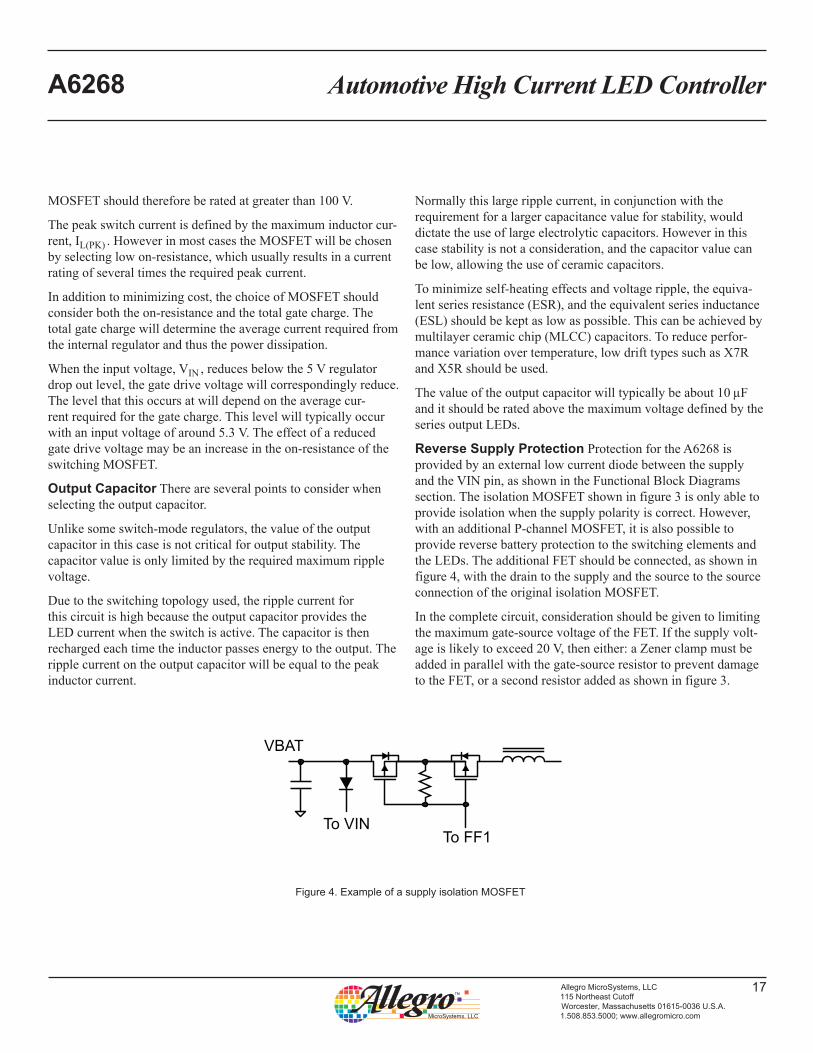
Reverse Supply Protection Protection for the A6268 is provided by an external low current diode between the supply andtheVINpin,asshownintheFunctionalBlockDiagramssection. The isolation MOSFET shown in figure 3 is only able to provideisolationwhenthesupplypolarityiscorrect.However,with an additional P-channel MOSFET, it is also possible to provide reverse battery protection to the switching elements and the LEDs. The additional FET should be connected, as shown in figure 4, with the drain to the supply and the source to the source connection of the original isolation MOSFET.
In the complete circuit, consideration should be given to limiting the maximum gate-source voltage of the FET. If the supply volt-age is likely to exceed 20 V, then either: a Zener clamp must be added in parallel with the gate-source resistor to prevent damage to the FET, or a second resistor added as shown in figure 3.
For Reference Only; not for tooling use (reference MO-153 ABT)Dimensions in millimetersDimensions exclusive of mold flash, gate burrs, and dambar protrusions Exact case and lead configuration at supplier discretion within limits shown
B
CExposed thermal pad (bottom surface); dimensions may vary with device
6.10
0.650.45
1.70
3.00
3.00
16
21
Reference land pattern layout (reference IPC7351 SOP65P640X110-17M); All pads a minimum of 0.20 mm from all adjacent pads; adjust as necessary to meet application process requirements and PCB layout tolerances; when mounting on a multilayer PCB, thermal vias at the exposed thermal pad land can improve thermal dissipation (reference EIA/JEDEC Standard JESD51-5)
Allegro’s products are not to be used in life support devices or systems, if a failure of an Allegro product can reasonably be expected to cause the failure of that life support device or system, or to affect the safety or effectiveness of that device or system.Theinformationincludedhereinisbelievedtobeaccurateandreliable.However,AllegroMicroSystems,LLCassumesnoresponsibilityforitsuse;norforanyinfringementofpatentsorotherrightsofthirdpartieswhichmayresultfromitsuse.
Revision HistoryRevision Revision Date Description of Revision
Rev. 2 April 1, 2013 Update fMIN
Rev. 3 June 19, 2014 At start up, or during pulse width modulation of the enable pin, the fault detection circuitry associated with the LED Sense Resistor Negative Overcurrent protection is inactive for a period defined by the fault blank timer, tFB.