Description The ADNS-3080 is a high performance addition to PixArt Imaging popular ADNS family of optical mouse sensors. The ADNS-3080 is based on a new, faster architecture with improved navigation. The sensor is capable of sensing high speed mouse motion - up to 40 inches per second and acceleration up to 15g – for increased user precision and smoothness. The ADNS-3080 along with the ADNS-2120-001 trim lens, ADNS-2220-001 assembly clip and HLMP-EG3E-xxxxx led form a complete, compact optical mouse tracking system. There are no moving parts, which means high reliability and less maintenance for the end user. In addition, precision optical alignment is not required, facilitating high volume assembly. The sensor is programmed via registers through a four-wire serial port. It is packaged in a 20-pin staggered dual inline package (DIP). Theory of Operation The ADNS-3080 is based on Optical Navigation Technol- ogy, which measures changes in position by optically acquiring sequential surface images (frames) and math- ematically determining the direction and magnitude of movement. It contains an Image Acquisition System (IAS), a Digital Signal Processor (DSP), and a four-wire serial port. The IAS acquires microscopic surface images via the lens and illumination system. These images are processed by the DSP to determine the direction and distance of motion. The DSP calculates the Δx and Δy relative dis- placement values. An external microcontroller reads the Δx and Δy informa- tion from the sensor serial port. The microcontroller then translates the data into PS2 or USB signals before sending them to the host PC or game console. Features High speed motion detection – up to 40 ips and 15g New architecture for greatly improved optical navigation technology Programmable frame rate over 6400 frames per second SmartSpeed self-adjusting frame rate for optimum performance Serial port burst mode for fast data transfer 400 or 1600 cpi selectable resolution Single 3.3 volt power supply Four-wire serial port along with Chip Select, Power Down, and Reset pins Applications Mice for game consoles and computer games Mice for desktop PC’s, Workstations, and portable PC’s Trackballs Integrated input devices ADNS-3080 High-Performance Optical Mouse Sensor Data Sheet All rights strictly reserved any portion in this paper shall not be reproduced, copied or transformed to any other forms without permission. PixArt Imaging Inc. E-mail: [email protected]
Transcript
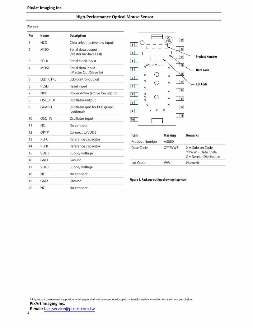
Description
The ADNS-3080 is a high performance addition to PixArt Imaging popular ADNS family of optical mouse sensors.
The ADNS-3080 is based on a new, faster architecture with improved navigation. The sensor is capable of sensing high speed mouse motion - up to 40 inches per second and acceleration up to 15g – for increased user precision and smoothness.
The ADNS-3080 along with the ADNS-2120-001 trim lens, ADNS-2220-001 assembly clip and HLMP-EG3E-xxxxx led form a complete, compact optical mouse tracking system. There are no moving parts, which means high reliability and less maintenance for the end user. In addition, precision optical alignment is not required, facilitating high volume assembly.
The sensor is programmed via registers through a four-wire serial port. It is packaged in a 20-pin staggered dual inline package (DIP).
Theory of Operation
The ADNS-3080 is based on Optical Navigation Technol-ogy, which measures changes in position by optically acquiring sequential surface images (frames) and math-ematically determining the direction and magnitude of movement.
It contains an Image Acquisition System (IAS), a Digital Signal Processor (DSP), and a four-wire serial port.
The IAS acquires microscopic surface images via the lens and illumination system. These images are processed by the DSP to determine the direction and distance of motion. The DSP calculates the Δx and Δy relative dis-placement values.
An external microcontroller reads the Δx and Δy informa-tion from the sensor serial port. The microcontroller then translates the data into PS2 or USB signals before sending them to the host PC or game console.
Features
High speed motion detection – up to 40 ips and 15g
New architecture for greatly improved optical
navigation technology
Programmable frame rate over 6400 frames per second
SmartSpeed self-adjusting frame rate for optimum performance
Serial port burst mode for fast data transfer
400 or 1600 cpi selectable resolution
Single 3.3 volt power supply
Four-wire serial port along with Chip Select, Power Down, and Reset pins
Applications
Mice for game consoles and computer games
Mice for desktop PC’s, Workstations, and portable PC’s
Trackballs
Integrated input devices
ADNS-3080High-Performance Optical Mouse Sensor
Data Sheet
All rights strictly reserved any portion in this paper shall not be reproduced, copied or transformed to any other forms without permission.
CAUTION: It is advised that normal static precautions be taken in handling and assembly of this component to prevent damage and/or degradation which may be induced by ESD.
Section A-A
(3.67)
0.144
1.82 ± 0.03
0.071 ± 0.001
( 1.5 ~ Draft)AA
Pin #1
6.025
0.237
4.55
0.179
7.28 ± 0.03
0.287 ± 0.00113.38
0.527
∅ 5.60 ± 0.03
0.220 ± 0.001
∅ 1.05 ± 0.03
0.041 ± 0.001
Lead Width0.50
0.020
22.30
0.878
(1.21)
0.048
(4.86)
0.191
Lead Offset1.00
0.039Lead Pitch
2.00
0.079 Chamfer0.3
0.012
Kapton Tape
9.10
0.358
12.85(At Shoulder)
0.506
(6.43)
0.253
0.25
0.010
0.99
0.039
3.18
0.125
7.05
0.278
12.85 ± 0.74 (At Lead Tip)
0.506 ± 0.029
2.25 ± 0.03
0.089 ± 0.001
90 ± 3
Features for Illustration only
Lot Code
Product NumberDate Code
Pin #1
Notes:
1. Dimensions in millimeters / inches.
2. Dimensional tolerance: ±0.1mm.
3. Coplanarity of leads: 0.1mm.
4. Lead pitch tolerance: ±0.15mm.
5. Non-cumulative pitch tolerance: ±0.15mm.
6. Angular tolerance: ±3.0
7. Maximum flash: 0.2mm.
8. Chamfer (25 x 2) on the taper side of the lead.
9. () These dimensions are for reference only and should
not be used to mechanically reference the sensor.
10. Document Number: LED_Spts_20A_Pkg_001.
All rights strictly reserved any portion in this paper shall not be reproduced, copied or transformed to any other forms without permission.
surface at the optimum angle. Features on the lens align it to the sensor, base plate, and clip with the LED. The lens also has a large round fl ange to provide a long creepage path for any ESD events that occur at the opening of the base plate.
The ADNS-2220-001 clip holds the LED in relation to the lens. The LED must be inserted into the clip and the LED’s leads formed prior to loading on the PCB. The clip interlocks the sensor to the lens, and through the lens to the alignment features on the base plate.
The HLMP-EG3E-xxxxx LED is recommended for illumina-tion. If used with the bin table, suffi cient illumination can be guaranteed.
Figure 3. Recommended PCB mechanical cutouts and spacing
2D Assembly Drawing of ADNS-3080
Shown with ADNS-2120-001 trim lens, ADNS-2220-001 assembly clip and HLMP-EG3E-xxxxx led.
PixArt Imaging provides an IGES fi le drawing de-scribing the base plate molding features for lens and PCB alignment.
The components interlock as they are mounted onto defi ned features on the base plate.
The ADNS-3080 sensor is designed for mounting on a through hole PCB, looking down. There is an aperture stop and features on the package that align to the lens.
The ADNS-2120-001 trim lens provides optics for the imaging of the surface as well as illumination of the
Overview of Optical Mouse Sensor Assembly
2X ∅
Dimensions in millimeters / inches
43.131.698
42.531.674
39.061.538
3.550.140
1.500.059
12.600.496
11.380.448
1.280.050
20X ∅ 0.800.031
0
1.220.048
3.220.127
15.880.62513.88
0.5467.60
0.2995.06
0.199
1.000.039
28.131.107
29.501.161
Recommended
Clear Zone
0
All rights strictly reserved any portion in this paper shall not be reproduced, copied or transformed to any other forms without permission.
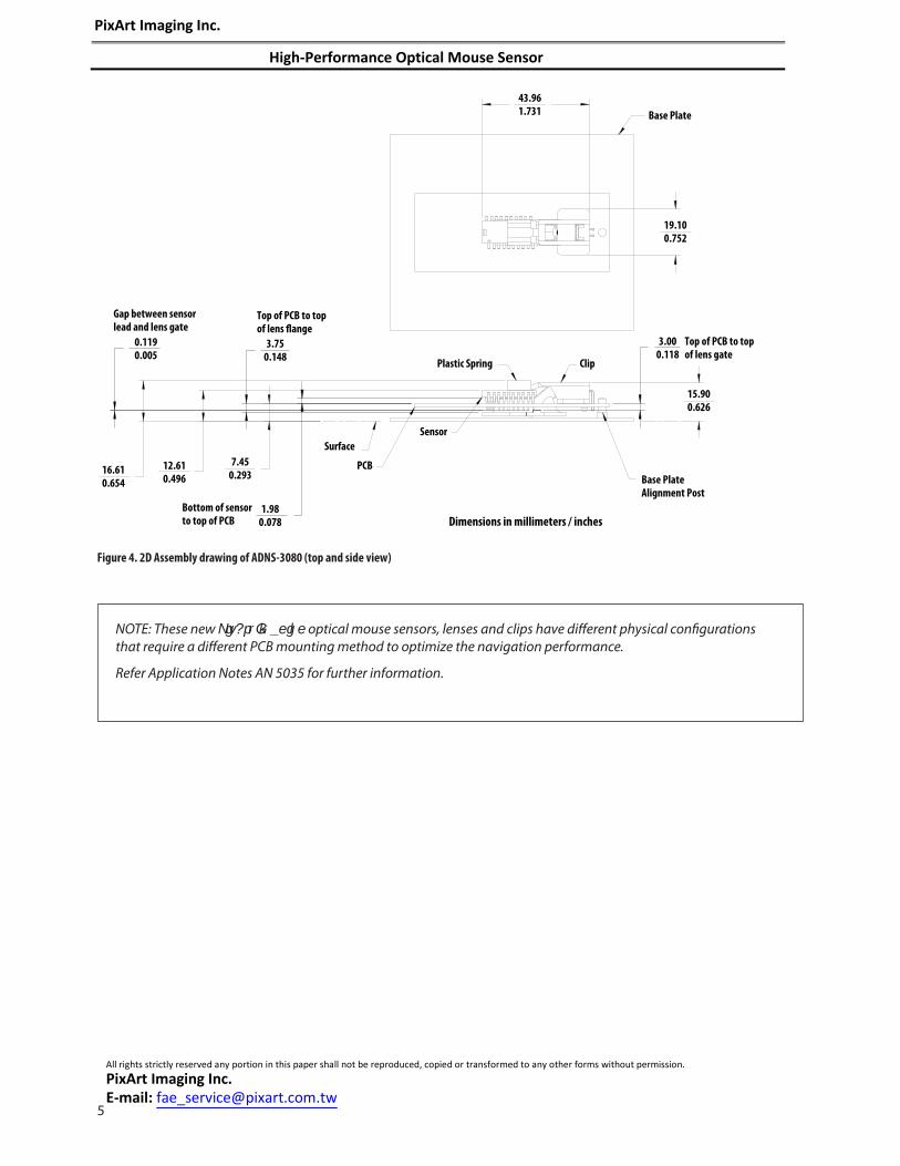
Figure 4. 2D Assembly drawing of ADNS-3080 (top and side view)
NOTE: These new optical mouse sensors, lenses and clips have diff erent physical confi gurations that require a diff erent PCB mounting method to optimize the navigation performance.
Refer Application Notes AN 5035 for further information.
43.961.731
Gap between sensorlead and lens gate
Dimensions in millimeters / inches
Top of PCB to topof lens flange
Top of PCB to topof lens gate
Base PlateAlignment Post
Plastic Spring
Sensor
Clip
Surface
PCB
Bottom of sensorto top of PCB
16.610.654
12.610.496
7.450.293
0.1190.005
3.750.148
15.900.626
3.000.118
19.100.752
Base Plate
1.980.078
All rights strictly reserved any portion in this paper shall not be reproduced, copied or transformed to any other forms without permission.
1. Insert the sensor and all other electrical components into PCB.
2. Insert the LED into the assembly clip and bend the leads 90 degrees.
3. Insert the LED/clip assembly into PCB.
4. This sensor package is only qualifi ed for wave-solder process.
5. Wave Solder the entire assembly in a no-wash solder process utilizing solder fi xture. The solder fi xture is needed to protect the sensor during the solder pro-cess. It also sets the correct sensor-to -PCB distance as the lead shoulders do not normally rest on the PCB surface. The fi xture should be designed to expose the sensor leads to solder while shielding the optical aperture from direct solder contact.
Figure 6. Block diagram of ADNS-3080 optical mouse sensor
IMAGEPROCESSOR
REFERENCEVOLTAGEFILTER NODE
3.3 V POWER
REFB
REFC
GND
RESONATOR OSC_IN
OSC_OUT
MOSI
NCS
SCLK
OPTP
V DD3
MISO
LED_CTRL
RESET
NPD
VO
LTA
GE
REG
ULA
TOR
AN
D P
OW
ER C
ON
TRO
L
Seri
al P
ort
CTRL
OSCILLATOR
6. Place the lens onto the base plate.
7. Remove the protective kapton tape from optical ap-erture of the sensor. Care must be taken to keep con-taminants from entering the aperture. During mouse assembly process, it is recommended that the PCB is held vertically when kapton tapes are being removed.
8. Insert PCB assembly over the lens onto the base plate aligning post to retain PCB assembly. The sensor ap-erture ring should self-align to the lens.
9. The optical position reference for the PCB is set by the base plate and lens. Note that the PCB motion due to button presses must be minimized to maintain optical alignment.
10. Install mouse top case. There MUST be a feature in the top case to press down.
HLMP-EG3E-xxxxx (LED)
ADNS-2220-001 (Clip)
ADNS-3080 (Sensor)
Customer supplied PCB
ADNS-2120-001 (Trim Lens)
Customer supplied base plate
with recommended alignment
features per IGES drawing.
All rights strictly reserved any portion in this paper shall not be reproduced, copied or transformed to any other forms without permission.
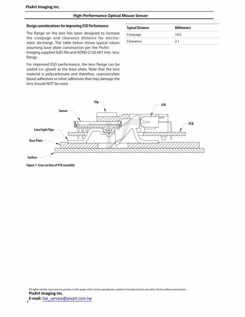
Design considerations for improving ESD Performance
The fl ange on the lens has been designed to increase the creepage and clearance distance for electro-static discharge. The table below shows typical values assuming base plate construction per the PixArt Imaging supplied IGES fi le and ADNS-2120-001 trim lens fl ange.
For improved ESD performance, the lens fl ange can be sealed (i.e. glued) to the base plate. Note that the lens material is polycarbonate and therefore, cyanoacrylate based adhesives or other adhesives that may damage the lens should NOT be used.
ClipLED
PCB
Sensor
Lens/Light Pipe
Surface
Base Plate
Typical Distance Millimeters
Creepage 16.0
Clearance 2.1
All rights strictly reserved any portion in this paper shall not be reproduced, copied or transformed to any other forms without permission.
Figure 8. Schematic Diagram for USB, PS/2 mouse application with ADNS-3080
Notes• Caps for pins 15 and 17 MUST have trace lengths LESS than 5 mm to nearest ground pin.• Pins 15 and 17 caps MUST use pin 16 GND. • Pin 9, if used, should not be connected to PCB GND to reduce potential RF emissions.• The 0.1 uF caps must be ceramic.• Caps should have less than 5 nH of self inductance.• Caps should have less than 0.2 Ω ESR.• NC pins should not be connected to any traces.• Surface mount parts are recommended.• Care must be taken when interfacing a 5V microcontroller to the ADNS-3080. Serial port inputs on the sensor should be connected to open-
drain outputs from the microcontroller or use an active drive level shifter. NPD and RESET should be connected to 5V microcontroller outputs through a resistor divider or other level shifting technique.
• VDD3 and GND should have low impedance connections to the power supply.• Capacitors connected to pin 15 and 17 should be connected to pin 16 and then to pin 19.
AD
NS-
3080
CYP
RES
S
CY7C
6374
3A-P
C
0.1uF
14
10
Vcc
Vpp
9VSS
Ceramic Resonator
Murata
CSALS 24 M 0X 53 -B 0
TDK FCR 24. 0 M 2G
17
5
V DD
LED_CTRL
SURFACE
InternalImage
Sensor
ADNS2120Lens
HLMP-EG3E-xxxxx
24 MHz
8
10
OSC_OUT
OSC_IN
15
GND
24
P0.5*
3
P0.4*
4
6
MOSI
RESETP0.2
23
1.3 KΩ
16
15D -
D +
Vreg11
P1.7
P1.5
P1.4
17
18
7
Vcc
D +
D -
GND
SHLD
6 MHz
1213
XTALINXTALOUT
(Optional)
6
5
P1.2
P1.0
Buttons
L
M
V DD
19
16 GND
REFB14
P0.3 7NPD
4
P0.7*3
SCLK21
P0.62
MISO22
9GUARD
NC
NC
11 18
20P1.1 R
20KΩ20KΩ
1NCS
LP2950ACZ-3.3
13REFC
2.2uF
187Ω1/8 W
Vcc
Vo 3.3V12
OPTP
NC
20
10 KΩ
10 KΩ
Vcc
Vcc
QA
QB
ALPSEC10E
Scroll WheelEncoder
1
2
3
20kΩ
20kΩ
0.1uF
4.7uF
0.1uF
Vin Vo
GND
2
4.7uF
+0.1uF
3 1
BS170
+
+
Notes:
- All capacitors close to chip
- 24MHz and 6MHz oscillators close to chip
- * Outputs configured as open drain
All rights strictly reserved any portion in this paper shall not be reproduced, copied or transformed to any other forms without permission.
For best tracking performance,SROM is required to be loaded into ADNS-3080. This architecture enables immediate adoption of new features and improved per-formance algorithms. The external program is supplied by PixArt Imaging as a fi le which may be burned into a programmable device. A micro-controller with suffi cient memory may be used. On power-up and reset, the ADNS-3080 program is downloaded into volatile memory using the burst-mode procedure described in the Synchronous Serial Port section. The program size is 1986 x 8 bits.
Regulatory Requirements
Passes FCC B and worldwide analogous emission limits when assembled into a mouse with shielded cable and following PixArt Imaging’ recommendations.
Passes IEC-1000-4-3 radiated susceptibility level when assembled into a mouse with shielded cable and fol-lowing PixArt Imaging’ recommendations.
Passes EN61000-4-4/IEC801-4 EFT tests when assem-bled into a mouse with shielded cable and following PixARt Imaging ’ recommendations.
UL fl ammability level UL94 V-0.
Provides suffi cient ESD creepage/clearance distance to avoid discharge up to 15kV when assembled into a mouse according to usage instructions above.
Figure 9. Distance from lens reference plane to surface
Sensor
Lens
Object Surface
2.40
0.094
All rights strictly reserved any portion in this paper shall not be reproduced, copied or transformed to any other forms without permission.
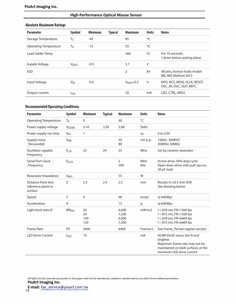
Frame Rate FR 2000 6469 Frames/s See Frame_Period register section
LED Drive Current ILED 10 mA HLMP-EG3E-xxxxx, bin N and brighter.Maximum frame rate may not be maintained on dark surfaces at the minimum LED drive current
All rights strictly reserved any portion in this paper shall not be reproduced, copied or transformed to any other forms without permission.
Electrical Characteristics over recommended operating conditions. Typical values at 25 °C, VDD3=3.3V, fclk=24MHz.
Parameter Symbol Min. Typical Max. Units Notes
VDD to RESET tOP 250 s From VDD = 3.0V to RESET sampled
Data delay after RESET
tPU-RESET 35 ms From RESET falling edge to valid motion data at 2000 fps and shutter bound 8290.
Input delay after reset
TIN-RST 500 s From RESET falling edge to inputs active (NPD, MOSI, NCS, SCLK)
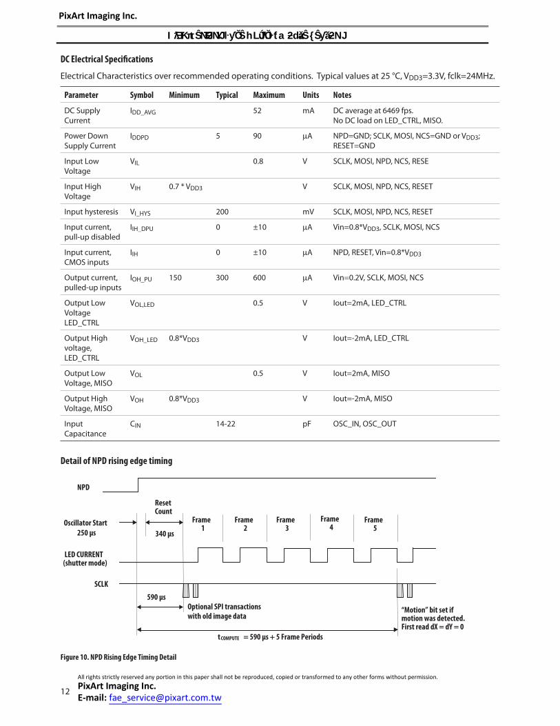
Power Down tPD 2.1 ms From NPD falling edge to initiate the power down cycle at 500fps (tpd = 1 frame period + 100ms )
Wake from NPD tPUPD 75 ms From NPD rising edge to valid motion data at 2000 fps and shutter bound 8290. Max assumes surface change while NPD is low.
Data delay after NPD
tCOMPUTE 3.1 ms From NPD rising edge to all registers contain data from new images at 2000fps (see Figure 10) .
RESET pulse width tPW-RESET 10 s
MISO rise time tr-MISO 40 200 ns CL = 50pF
MISO fall time tf-MISO 40 200 ns CL = 50pF
MISO delay afterSCLK
tDLY-MISO 120 ns From SCLK falling edge to MISO data valid, no load conditions
MISO hold time thold-MISO 250 ns Data held until next falling SCLK edge
MOSI hold time thold-MOSI 200 ns Amount of time data is valid after SCLK rising edge
MOSI setup time tsetup-MOSI 120 ns From data valid to SCLK rising edge
SPI time betweenwrite commands
tSWW 50 s From rising SCLK for last bit of the fi rst data byte, to rising SCLK for last bit of the second data byte.
SPI time between write and read commands
tSWR 50 s From rising SCLK for last bit of the fi rst data byte, to rising SCLK for last bit of the second address byte.
SPI time between read and subsequent commands
tSRWtSRR
250 ns From rising SCLK for last bit of the fi rst data byte, to falling SCLK for fi rst bit of the second address byte.
SPI read address-data delay
tSRAD 50 s From rising SCLK for last bit of the address byte, to falling SCLK for fi rst bit of data being read. All registers except Motion & Motion_Burst
SPI motion read address-data delay
tSRAD-MOT 75 s From rising SCLK for last bit of the address byte, to falling SCLK for fi rst bit of data being read. Applies to 0x02 Motion, and 0x50 Motion_Burst, registers
NCS to SCLK active tNCS-SCLK 120 ns From NCS falling edge to fi rst SCLK rising edge
SCLK to NCS inactive tSCLK-NCS 120 ns From last SCLK falling edge to NCS rising edge, for valid MISO data transfer
NCS to MISO high-Z tNCS-MISO 250 ns From NCS rising edge to MISO high-Z state
SROM download and frame capture byte-to-byte delay
tLOAD 10 s (see Figure 23 and 24)
NCS to burst mode exit
tBEXIT 4 s Time NCS must be held high to exit burst mode
Transient SupplyCurrent
IDDT 85 mA Max supply current during a VDD3 ramp from 0 to 3.6V
All rights strictly reserved any portion in this paper shall not be reproduced, copied or transformed to any other forms without permission.
The synchronous serial port is used to set and read pa-rameters in the ADNS-3080, and to read out the motion information. The serial port is also used to load SROM data into the ADNS-3080.
The port is a four-wire, serial port. The host micro-con-troller always initiates communication; the ADNS-3080 never initiates data transfers. The serial port cannot be activated while the chip is in power down mode (NPD low) or reset (RESET high). SCLK, MOSI, and NCS may be driven directly by a 3.3V output from a micro-controller, or they may be placed in an open drain confi guration by enabling on-chip pull-up current sources. The open drain drive allows the use of a 5V micro-controller without any level shifting components. The port pins may be shared with other SPI slave devices. When the NCS pin is high, the inputs are ignored and the output is tri-stated.
The lines which comprise the SPI port are:
SCLK: Clock input. It is always generated by the master (the micro- controller).
MOSI: Input data (Master Out/Slave In).
MISO: Output data (Master In/Slave Out).
NCS: Chip select input (active low).
NCS needs to be low to activate the serial port; otherwise, MISO will be high-Z, and MOSI & SCLK will be ignored. NCS can also be used to reset the serial port in case of an error.
Chip Select Operation
The serial port is activated after NCS goes low. If NCS is raised during a transaction, the entire transaction is aborted and the serial port will be reset. This is true for all transactions including SROM download. After a transaction is aborted, the normal address-to-data or transaction-to-transaction delay is still required before beginning the next transaction. To improve communica-tion reliability, all serial transactions should be framed by NCS. In other words, the port should not remain enabled during periods of non-use because ESD and EFT/B events could be interpreted as serial communication and put the chip into an unknown state. In addition, NCS must be raised after each burst-mode transaction is complete to terminate burst-mode. The port is not available for further use until burst-mode is terminated.
All rights strictly reserved any portion in this paper shall not be reproduced, copied or transformed to any other forms without permission.
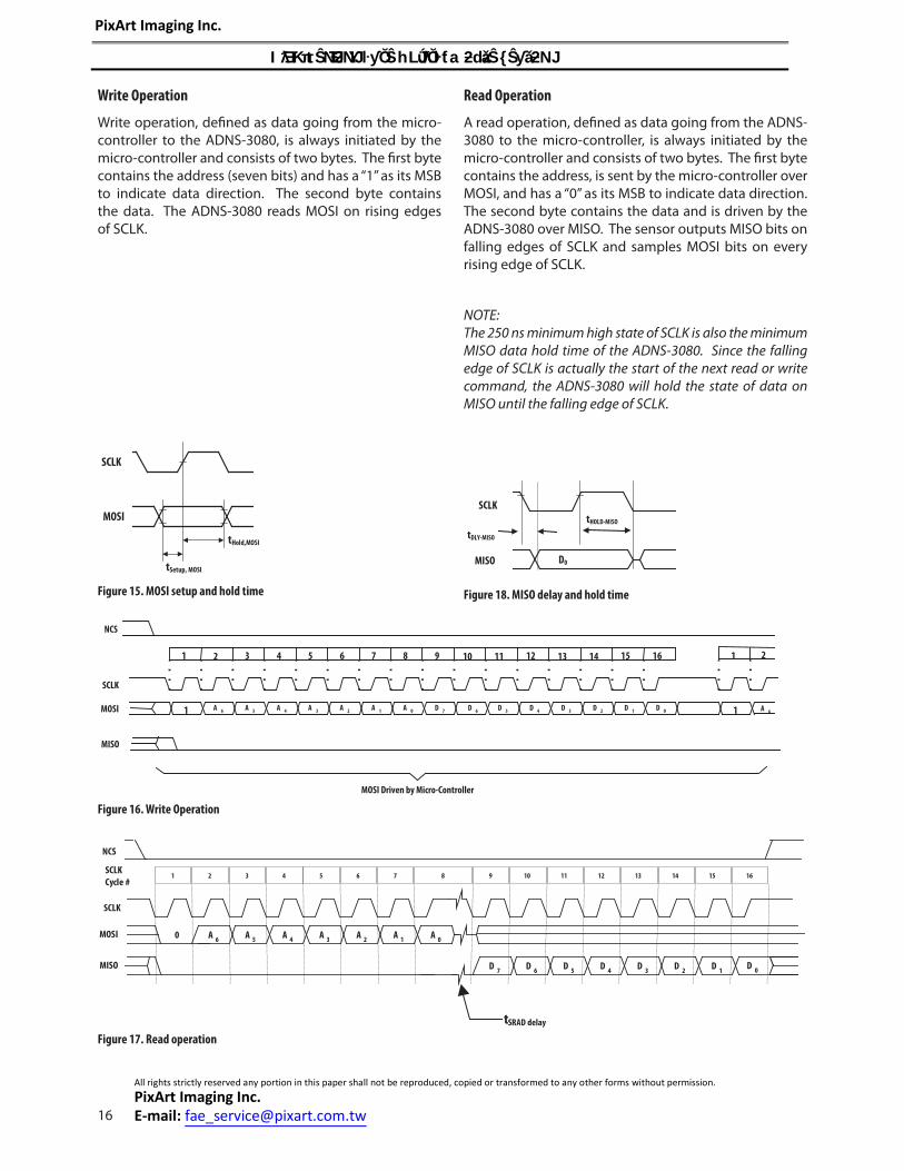
Write operation, defi ned as data going from the micro-controller to the ADNS-3080, is always initiated by the micro-controller and consists of two bytes. The fi rst byte contains the address (seven bits) and has a “1” as its MSB to indicate data direction. The second byte contains the data. The ADNS-3080 reads MOSI on rising edges of SCLK.
Figure 18. MISO delay and hold time
Read Operation
A read operation, defi ned as data going from the ADNS-3080 to the micro-controller, is always initiated by the micro-controller and consists of two bytes. The fi rst byte contains the address, is sent by the micro-controller over MOSI, and has a “0” as its MSB to indicate data direction. The second byte contains the data and is driven by the ADNS-3080 over MISO. The sensor outputs MISO bits on falling edges of SCLK and samples MOSI bits on every rising edge of SCLK.
NOTE: The 250 ns minimum high state of SCLK is also the minimum MISO data hold time of the ADNS-3080. Since the falling edge of SCLK is actually the start of the next read or write command, the ADNS-3080 will hold the state of data on MISO until the falling edge of SCLK.
SCLK
MOSI
tSetup, MOSI
tHold,MOSI
A 6 A 5 A 2 A 3 A 4 A 0 A 1 D 7 D 4 D 5 D 6 D 0 D 1 D 2 D 3
15 7 8 9 10 11 12 13 14 16 2 3 4 5 6
1
1
1
1
A 6
2
SCLK
MOSI
NCS
MISO
MOSI Driven by Micro-Controller
SCLK
MISO D0
tHOLD-MISO
tDLY-MISO
Figure 16. Write Operation
All rights strictly reserved any portion in this paper shall not be reproduced, copied or transformed to any other forms without permission.
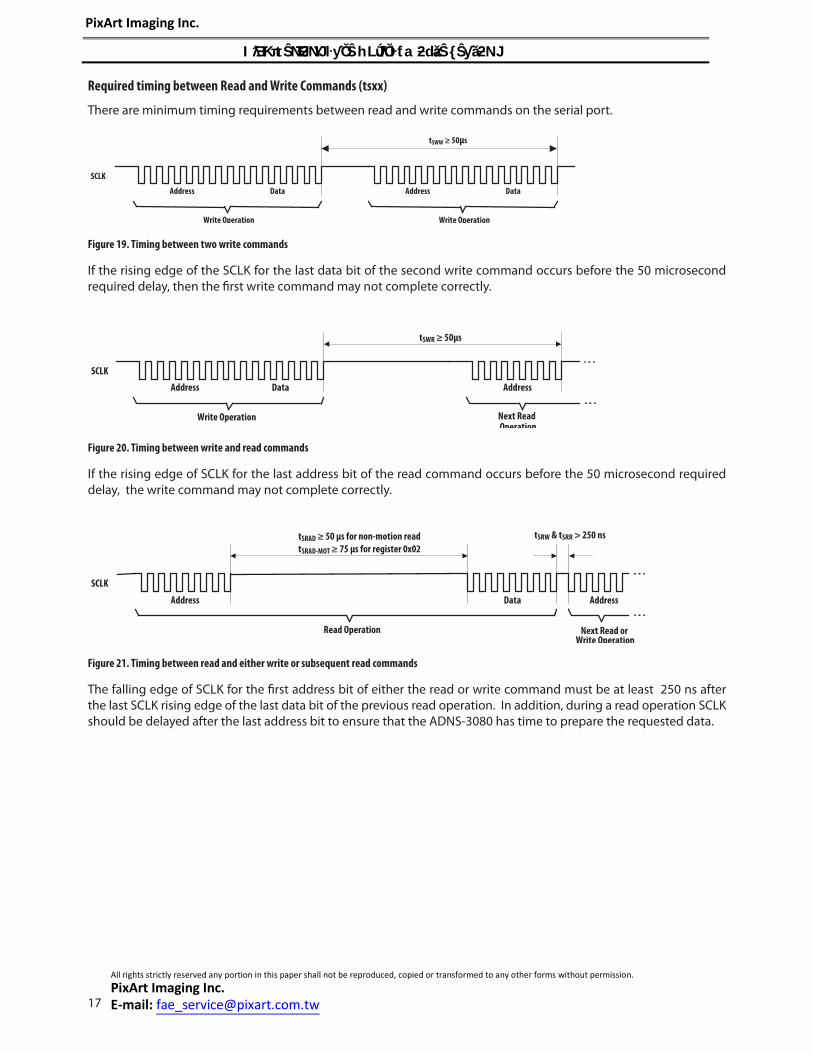
Required timing between Read and Write Commands (tsxx)
There are minimum timing requirements between read and write commands on the serial port.
Figure 19. Timing between two write commands
If the rising edge of the SCLK for the last data bit of the second write command occurs before the 50 microsecond required delay, then the fi rst write command may not complete correctly.
Figure 20. Timing between write and read commands
If the rising edge of SCLK for the last address bit of the read command occurs before the 50 microsecond required delay, the write command may not complete correctly.
Figure 21. Timing between read and either write or subsequent read commands
The falling edge of SCLK for the fi rst address bit of either the read or write command must be at least 250 ns after the last SCLK rising edge of the last data bit of the previous read operation. In addition, during a read operation SCLK should be delayed after the last address bit to ensure that the ADNS-3080 has time to prepare the requested data.
SCLK
Address Data
tSWW ≥ 50μs
Write Operation
Address Data
Write Operation
Address Data
Write Operation
Address
Next ReadOperation
SCLK
tSWR ≥ 50μs
tSRAD ≥ 50 μs for non-motion read
tSRAD-MOT ≥ 75 μs for register 0x02
tSRW & tSRR > 250 ns
Next Read orWrite Operation
Data
Read Operation
AddressAddress
SCLK
All rights strictly reserved any portion in this paper shall not be reproduced, copied or transformed to any other forms without permission.
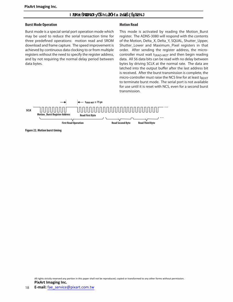
Burst mode is a special serial port operation mode which may be used to reduce the serial transaction time for three predefi ned operations: motion read and SROM download and frame capture. The speed improvement is achieved by continuous data clocking to or from multiple registers without the need to specify the register address, and by not requiring the normal delay period between data bytes.
Figure 22. Motion burst timing
Motion_Burst Register Address Read First Byte
First Read Operation Read Second Byte
SCLK
tSRAD-MOT ≥ 75 μs
Read Third Byte
Motion Read
This mode is activated by reading the Motion_Burst register. The ADNS-3080 will respond with the contents of the Motion, Delta_X, Delta_Y, SQUAL, Shutter_Upper, Shutter_Lower and Maximum_Pixel registers in that order. After sending the register address, the micro-controller must wait tSRAD-MOT and then begin reading data. All 56 data bits can be read with no delay between bytes by driving SCLK at the normal rate. The data are latched into the output buff er after the last address bit is received. After the burst transmission is complete, the micro-controller must raise the NCS line for at least tBEXIT to terminate burst mode. The serial port is not available for use until it is reset with NCS, even for a second burst transmission.
All rights strictly reserved any portion in this paper shall not be reproduced, copied or transformed to any other forms without permission.
This function is used to load the PixArt Imagingsupplied fi rmware fi le contents into the ADNS-3080. The fi rmware fi le is an ASCII text fi le with each 2-character byte (hexadecimal representation) on a single line.
This mode is activated by the following steps:
1. Perform hardware reset by toggling the RESET pin
2. Write 0x44 to register 0x20
3. Write 0x07 to register 0x23
4. Write 0x88 to register 0x24
5. Wait at least 1 frame period
6. Write 0x18 to register 0x14 (SROM_Enable register)
7. Begin burst mode write of data fi le to register 0x60 (SROM_Load register)
After the fi rst data byte is complete, the SROM or micro-controller must write subsequent bytes by presenting the data on the MOSI line and driving SCLK at the normal rate. A delay of at least tLOAD must exist between data
Figure 23. SROM download burst mode
bytes as shown. After the download is complete, the micro-controller must raise the NCS line for at least tBEXIT to terminate burst mode. The serial port is not available for use until it is reset with NCS, even for a second burst transmission.
PixArt Imaging recommends reading the SROM_ID register to verify that the download was successful. In addition, a self-test may be executed, which performs a CRC on the SROM contents and reports the results in a register. The test is initiated by writing a particular value to the SROM_Enable register; the result is placed in the Data_Out register. See those register descriptions for more details.
PixArt Imaging provides the data fi le for download; the fi le size is 1986 data bytes. The chip will ignore any additional bytes written to the SROM_Load register after the SROM fi le.
NCS
address key data address byte 0 MOSI
SCLK
tNCS -SCLK
SROM_Enable reg write SROM_Load reg write
exit burst mode
enter burst
mode
≥4μs
tLOAD tLOAD
byte 1 byte 1985
tBEXIT
>120ns
address
soonest to read SROM_ID
3 reg writes, see text
≥1 frame
period
≥40μs ≥10μs ≥10μs ≥10μs
≥100μs
All rights strictly reserved any portion in this paper shall not be reproduced, copied or transformed to any other forms without permission.
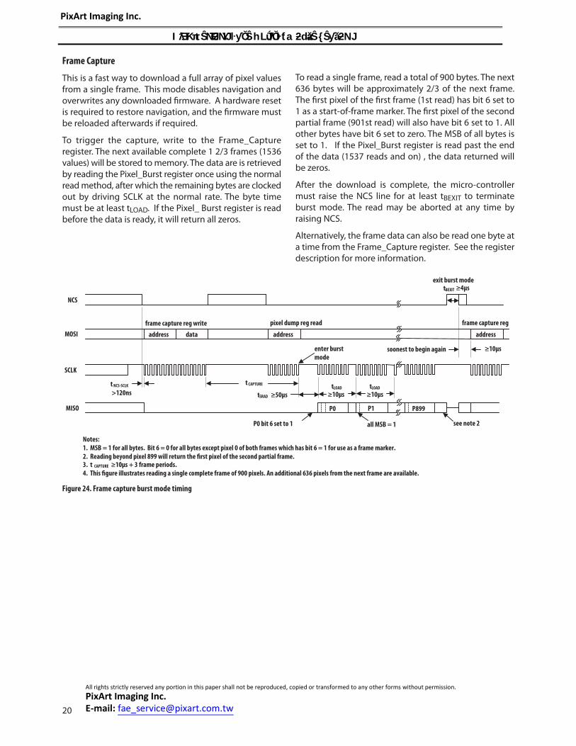
This is a fast way to download a full array of pixel values from a single frame. This mode disables navigation and overwrites any downloaded fi rmware. A hardware reset is required to restore navigation, and the fi rmware must be reloaded afterwards if required.
To trigger the capture, write to the Frame_Capture register. The next available complete 1 2/3 frames (1536 values) will be stored to memory. The data are is retrieved by reading the Pixel_Burst register once using the normal read method, after which the remaining bytes are clocked out by driving SCLK at the normal rate. The byte time must be at least tLOAD. If the Pixel_ Burst register is read before the data is ready, it will return all zeros.
To read a single frame, read a total of 900 bytes. The next 636 bytes will be approximately 2/3 of the next frame. The fi rst pixel of the fi rst frame (1st read) has bit 6 set to 1 as a start-of-frame marker. The fi rst pixel of the second partial frame (901st read) will also have bit 6 set to 1. All other bytes have bit 6 set to zero. The MSB of all bytes is set to 1. If the Pixel_Burst register is read past the end of the data (1537 reads and on) , the data returned will be zeros.
After the download is complete, the micro-controller must raise the NCS line for at least tBEXIT to terminate burst mode. The read may be aborted at any time by raising NCS.
Alternatively, the frame data can also be read one byte at a time from the Frame_Capture register. See the register description for more information.
Figure 24. Frame capture burst mode timing
NCS
address data address address MOSI
SCLK
P0 P1 P899 MISO
t NCS-SCLK
>120ns
frame capture reg write
enter burst
mode
t CAPTURE tLOAD
Notes:
1. MSB = 1 for all bytes. Bit 6 = 0 for all bytes except pixel 0 of both frames which has bit 6 = 1 for use as a frame marker.
2. Reading beyond pixel 899 will return the first pixel of the second partial frame.3. t CAPTURE ≥10μs + 3 frame periods.
4. This figure illustrates reading a single complete frame of 900 pixels. An additional 636 pixels from the next frame are available.
tLOAD
tSRAD
pixel dump reg read
P0 bit 6 set to 1 all MSB = 1 see note 2
soonest to begin again
frame capture reg
exit burst modetBEXIT
≥10μs≥10μs≥50μs
≥4μs
≥10μs
All rights strictly reserved any portion in this paper shall not be reproduced, copied or transformed to any other forms without permission.
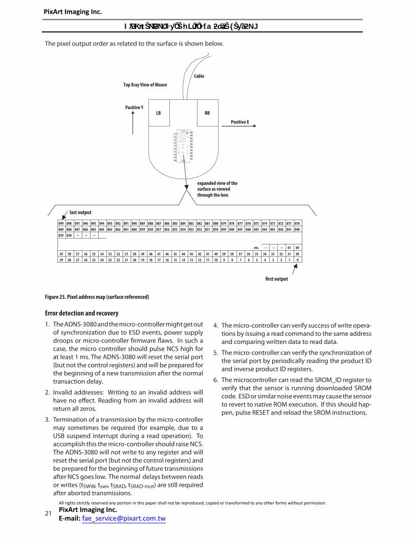
expanded view of thesurface as viewedthrough the lens
last output
first output
~ ~ ~
1
2
3
4
5
6
7
8
9
1011
12
13
14
15
16
17
18
19
20
Error detection and recovery
1. The ADNS-3080 and the micro-controller might get out of synchronization due to ESD events, power supply droops or micro-controller fi rmware fl aws. In such a case, the micro-controller should pulse NCS high for at least 1 ms. The ADNS-3080 will reset the serial port (but not the control registers) and will be prepared for the beginning of a new transmission after the normal transaction delay.
2. Invalid addresses: Writing to an invalid address will have no eff ect. Reading from an invalid address will return all zeros.
3. Termination of a transmission by the micro-controller may sometimes be required (for example, due to a USB suspend interrupt during a read operation). To accomplish this the micro-controller should raise NCS. The ADNS-3080 will not write to any register and will reset the serial port (but not the control registers) and be prepared for the beginning of future transmissions after NCS goes low. The normal delays between reads or writes (tSWW, tswr, tSRAD, tSRAD-mot) are still required after aborted transmissions.
4. The micro-controller can verify success of write opera-tions by issuing a read command to the same address and comparing written data to read data.
5. The micro-controller can verify the synchronization of the serial port by periodically reading the product ID and inverse product ID registers.
6. The microcontroller can read the SROM_ID register to verify that the sensor is running downloaded SROM code. ESD or similar noise events may cause the sensor to revert to native ROM execution. If this should hap-pen, pulse RESET and reload the SROM instructions.
All rights strictly reserved any portion in this paper shall not be reproduced, copied or transformed to any other forms without permission.
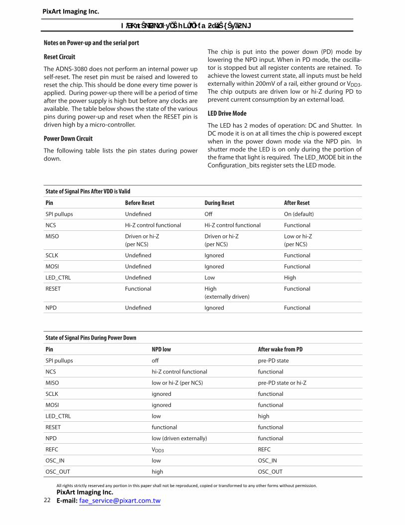
The ADNS-3080 does not perform an internal power up self-reset. The reset pin must be raised and lowered to reset the chip. This should be done every time power is applied. During power-up there will be a period of time after the power supply is high but before any clocks are available. The table below shows the state of the various pins during power-up and reset when the RESET pin is driven high by a micro-controller.
Power Down Circuit
The following table lists the pin states during power down.
State of Signal Pins After VDD is Valid
Pin Before Reset During Reset After Reset
SPI pullups Undefi ned Off On (default)
NCS Hi-Z control functional Hi-Z control functional Functional
MISO Driven or hi-Z(per NCS)
Driven or hi-Z(per NCS)
Low or hi-Z(per NCS)
SCLK Undefi ned Ignored Functional
MOSI Undefi ned Ignored Functional
LED_CTRL Undefi ned Low High
RESET Functional High(externally driven)
Functional
NPD Undefi ned Ignored Functional
State of Signal Pins During Power Down
Pin NPD low After wake from PD
SPI pullups off pre-PD state
NCS hi-Z control functional functional
MISO low or hi-Z (per NCS) pre-PD state or hi-Z
SCLK ignored functional
MOSI ignored functional
LED_CTRL low high
RESET functional functional
NPD low (driven externally) functional
REFC VDD3 REFC
OSC_IN low OSC_IN
OSC_OUT high OSC_OUT
The chip is put into the power down (PD) mode by lowering the NPD input. When in PD mode, the oscilla-tor is stopped but all register contents are retained. To achieve the lowest current state, all inputs must be held externally within 200mV of a rail, either ground or VDD3. The chip outputs are driven low or hi-Z during PD to prevent current consumption by an external load.
LED Drive Mode
The LED has 2 modes of operation: DC and Shutter. In DC mode it is on at all times the chip is powered except when in the power down mode via the NPD pin. In shutter mode the LED is on only during the portion of the frame that light is required. The LED_MODE bit in the Confi guration_bits register sets the LED mode.
All rights strictly reserved any portion in this paper shall not be reproduced, copied or transformed to any other forms without permission.
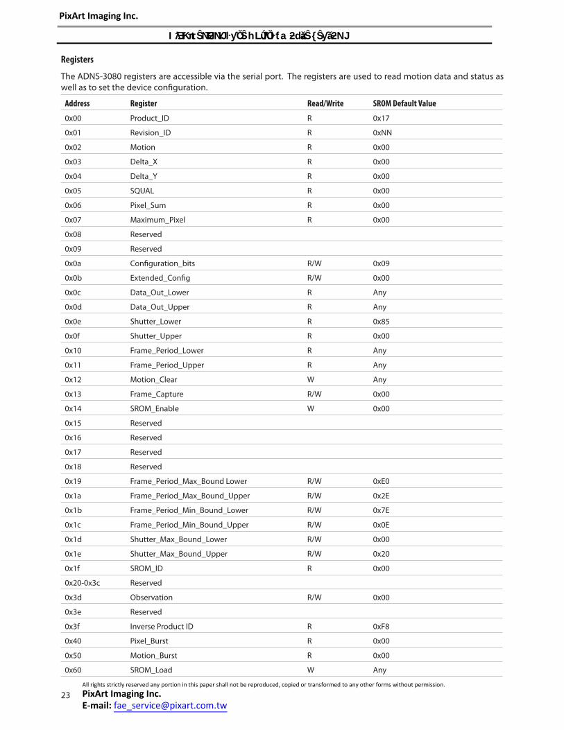
The ADNS-3080 registers are accessible via the serial port. The registers are used to read motion data and status as well as to set the device confi guration.
Address Register Read/Write SROM Default Value
0x00 Product_ID R 0x17
0x01 Revision_ID R 0xNN
0x02 Motion R 0x00
0x03 Delta_X R 0x00
0x04 Delta_Y R 0x00
0x05 SQUAL R 0x00
0x06 Pixel_Sum R 0x00
0x07 Maximum_Pixel R 0x00
0x08 Reserved
0x09 Reserved
0x0a Confi guration_bits R/W 0x09
0x0b Extended_Confi g R/W 0x00
0x0c Data_Out_Lower R Any
0x0d Data_Out_Upper R Any
0x0e Shutter_Lower R 0x85
0x0f Shutter_Upper R 0x00
0x10 Frame_Period_Lower R Any
0x11 Frame_Period_Upper R Any
0x12 Motion_Clear W Any
0x13 Frame_Capture R/W 0x00
0x14 SROM_Enable W 0x00
0x15 Reserved
0x16 Reserved
0x17 Reserved
0x18 Reserved
0x19 Frame_Period_Max_Bound Lower R/W 0xE0
0x1a Frame_Period_Max_Bound_Upper R/W 0x2E
0x1b Frame_Period_Min_Bound_Lower R/W 0x7E
0x1c Frame_Period_Min_Bound_Upper R/W 0x0E
0x1d Shutter_Max_Bound_Lower R/W 0x00
0x1e Shutter_Max_Bound_Upper R/W 0x20
0x1f SROM_ID R 0x00
0x20-0x3c Reserved
0x3d Observation R/W 0x00
0x3e Reserved
0x3f Inverse Product ID R 0xF8
0x40 Pixel_Burst R 0x00
0x50 Motion_Burst R 0x00
0x60 SROM_Load W Any
All rights strictly reserved any portion in this paper shall not be reproduced, copied or transformed to any other forms without permission.
USAGE: This register contains a unique identifi cation assigned to the ADNS-3080. The value in this register does not change; it can be used to verify that the serial communications link is functional.
Revision_ID Address: 0x01
Access: Read Reset Value: 0xNN
Data Type: 8-Bit unsigned integer.
USAGE: This register contains the IC revision. It is subject to change when new IC versions are released.
NOTE: The downloaded SROM fi rmware revision is a separate value and is available in the SROM_ID register.
Motion Address: 0x02
Access: Read Reset Value: 0x00
Data Type: Bit fi eld.
USAGE: Register 0x02 allows the user to determine if motion has occurred since the last time it was read. If so, then the user should read registers 0x03 and 0x04 to get the accumulated motion. It also tells if the motion buff ers have overfl owed, and the current resolution setting.
Bit 7 6 5 4 3 2 1 0
Field PID7 PID6 PID5 PID4 PID3 PID2 PID1 PID0
Bit 7 6 5 4 3 2 1 0
Field RID7 RID6 RID5 RID4 RID3 RID2 RID1 RID0
Bit 7 6 5 4 3 2 1 0
Field MOT Reserved Reserved OVF Reserved Reserved Reserved RES
Field Name Description
MOTMotion since last report or PD0 = No motion
1 = Motion occurred, data ready for reading in Delta_X and Delta_Y registers
Reserved Reserved
Reserved Reserved
OVF Motion overfl ow, Delta_Y and/or Delta_X buff er has overfl owed since last report0 = no overfl ow
1 = Overfl ow has occurred
Reserved Reserved
Reserved Reserved
Reserved Reserved
RES Resolution in counts per inch0 = 400
1 = 1600
All rights strictly reserved any portion in this paper shall not be reproduced, copied or transformed to any other forms without permission.
Notes for Motion: 1. Reading this register freezes the Delta_X and Delta_Y register values. Read this register before reading the Delta_X and Delta_Y registers. If
Delta_X and Delta_Y are not read before the motion register is read a second time, the data in Delta_X and Delta_Y will be lost. 2. PixArt Imaging RECOMMENDS that registers 0x02, 0x03 and 0x04 be read sequentially. See Motion burst mode also.3. Internal buff ers can accumulate more than eight bits of motion for X or Y. If either one of the internal buff ers overfl ows, then absolute path data
is lost and the OVF bit is set. This bit is cleared once some motion has been read from the Delta_X and Delta_Y registers, and if the buff ers are not at full scale. Since more data is present in the buff ers, the cycle of reading the Motion, Delta_X and Delta_Y registers should be repeated until the motion bit (MOT) is cleared. Until MOT is cleared, either the Delta_X or Delta_Y registers will read either positive or negative full scale. If the motion register has not been read for long time, at 400 cpi it may take up to 16 read cycles to clear the buff ers, at 1600 cpi, up to 64 cycles. Alternatively, writing to the Motion_Clear register (register 0x12) will clear all stored motion at once.
Delta_X Address: 0x03
Access: Read Reset Value: 0x00
Data Type: Eight bit 2’s complement number.
USAGE: X movement is counts since last report. Absolute value is determined by resolution. Reading clears the register.
Bit 7 6 5 4 3 2 1 0
Field X7 X6 X5 X4 X3 X2 X1 X0
Bit 7 6 5 4 3 2 1 0
Field Y7 Y6 Y5 Y4 Y3 Y2 Y1 Y0
Delta_Y Address: 0x04
Access: Read Reset Value: 0x00
Data Type: Eight bit 2’s complement number.
USAGE: Y movement is counts since last report. Absolute value is determined by resolution. Reading clears the register.
00 01 02 7E 7F
+127+126+1 +2
FFFE8180
0-1-2-127-128Motion
Delta_X
00 01 02 7E 7F
+127+126+1 +2
FFFE8180
0-1-2-127-128Motion
Delta_Y
All rights strictly reserved any portion in this paper shall not be reproduced, copied or transformed to any other forms without permission.
Data Type: Upper 8 bits of a 10-bit unsigned integer.
USAGE: SQUAL (Surface Quality) is a measure of ¼ of the number of valid* features visible by the sensor in the current frame. Use the following formula to fi nd the total number of valid features.
Number of features = SQUAL register value *4
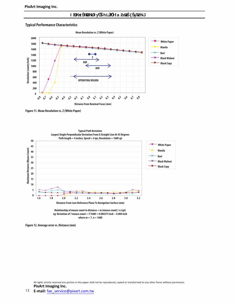
The maximum SQUAL register value is 169. Since small changes in the current frame can result in changes in SQUAL, variations in SQUAL when looking at a surface are expected. The graph below shows 250 sequentially acquired SQUAL values, while a sensor was moved slowly over white paper. SQUAL is nearly equal to zero, if there is no surface below the sensor. SQUAL is typically maximized when the navigation surface is at the optimum distance from the imaging lens (the nominal Z-height).
Bit 7 6 5 4 3 2 1 0
Field SQ7 SQ6 SQ5 SQ4 SQ3 SQ2 SQ1 SQ0
Figure 26. Squal values (white paper)
60
65
70
75
80
85
0 25 50 75 100 125 150 175 200 225 250
Squal Values (White Paper)
SQU
AL
Val
ue
All rights strictly reserved any portion in this paper shall not be reproduced, copied or transformed to any other forms without permission.
Data Type: High 8 bits of an unsigned 16-bit integer.
USAGE: This register is used to fi nd the average pixel value. It reports the upper byte of a 16-bit counter which sums all 900 pixels in the current frame. It may be described as the full sum divided by 256. To fi nd the average pixel value, use the following formula:
Average Pixel = Register Value * 256 / 900 = Register Value/3.51
The maximum register value is 221 (63 * 900/256 truncated to an integer). The minimum is 0. The pixel sum value can change on every frame.
Maximum_Pixel Address: 0x07
Access: Read Reset Value: 0x00
Data Type: Six bit number.
USAGE: Maximum Pixel value in current frame. Minimum value = 0, maximum value = 63. The maximum pixel value can vary with every frame.
Reserved Address: 0x08
Reserved Address: 0x09
Bit 7 6 5 4 3 2 1 0
Field AP7 AP6 AP5 AP4 AP3 AP2 AP1 AP0
Bit 7 6 5 4 3 2 1 0
Field 0 0 MP5 MP4 MP3 MP2 MP1 MP0
Figure 27. Mean squal vs. Z (white paper)
0
10
20
30
40
50
60
70
80
90
-1.0 -0.8 -0.6 -0.4 -0.2 0.0 0.2 0.4 0.6 0.8 1.0
Mean SQUAL vs Z (White Paper)
Delta from Nominal Focus (mm)
SQU
AL
Avg
Avg - 3sigma
Avg + 3sigma
All rights strictly reserved any portion in this paper shall not be reproduced, copied or transformed to any other forms without permission.
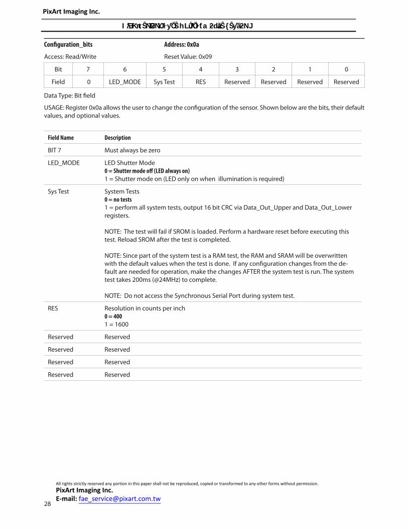
Field 0 LED_MODE Sys Test RES Reserved Reserved Reserved Reserved
Confi guration_bits Address: 0x0a
Access: Read/Write Reset Value: 0x09
Data Type: Bit fi eld
USAGE: Register 0x0a allows the user to change the confi guration of the sensor. Shown below are the bits, their default values, and optional values.
Field Name Description
BIT 7 Must always be zero
LED_MODE LED Shutter Mode0 = Shutter mode off (LED always on)
1 = Shutter mode on (LED only on when illumination is required)
Sys Test System Tests0 = no tests
1 = perform all system tests, output 16 bit CRC via Data_Out_Upper and Data_Out_Lower registers.
NOTE: The test will fail if SROM is loaded. Perform a hardware reset before executing this test. Reload SROM after the test is completed.
NOTE: Since part of the system test is a RAM test, the RAM and SRAM will be overwritten with the default values when the test is done. If any confi guration changes from the de-fault are needed for operation, make the changes AFTER the system test is run. The system test takes 200ms (@24MHz) to complete.
NOTE: Do not access the Synchronous Serial Port during system test.
RES Resolution in counts per inch0 = 400
1 = 1600
Reserved Reserved
Reserved Reserved
Reserved Reserved
Reserved Reserved
All rights strictly reserved any portion in this paper shall not be reproduced, copied or transformed to any other forms without permission.
USAGE: Register 0x0b allows the user to change the confi guration of the sensor. Shown below are the bits, their default values, and optional values.
Bit 7 6 5 4 3 2 1 0
Field Busy Reserved Reserved Reserved Reserved Serial_NPU NAGC Fixed_FR
Field Name Description
Busy Read-only bit. Indicates if it is safe to write to one or more of the following registers: Frame_Period_Max_Bound_Upper and Lower Frame_Period_Min_Bound_Upper and Lower Shutter_Max_Bound_Upper and LowerAfter writing to the Frame_Period_Max_Bound_Upper register, at least two frames must pass before writing again to any of the above registers. This bit may be used in lieu of a timer since the actual frame rate may not be known when running in auto mode.0 = writing to the registers is allowed
1 = do not write to the registers yet
Reserved Reserved
Reserved Reserved
Reserved Reserved
Reserved Reserved
Serial_NPU Disable serial port pull-up current sources0 = no, current sources are on
1 = yes, current sources are off
NAGC Disable AGC. Shutter will be set to the value in the Shutter_Max_Bound registers. 0 = no, AGC is active
1 = yes, AGC is disabled
Fixed_FR Fixed frame rate (disable automatic frame rate control). When this bit is set, the frame rate will be determined by the value in the Frame_Period_Max_Bound registers.0 = automatic frame rate
1 = fi xed frame rate
All rights strictly reserved any portion in this paper shall not be reproduced, copied or transformed to any other forms without permission.
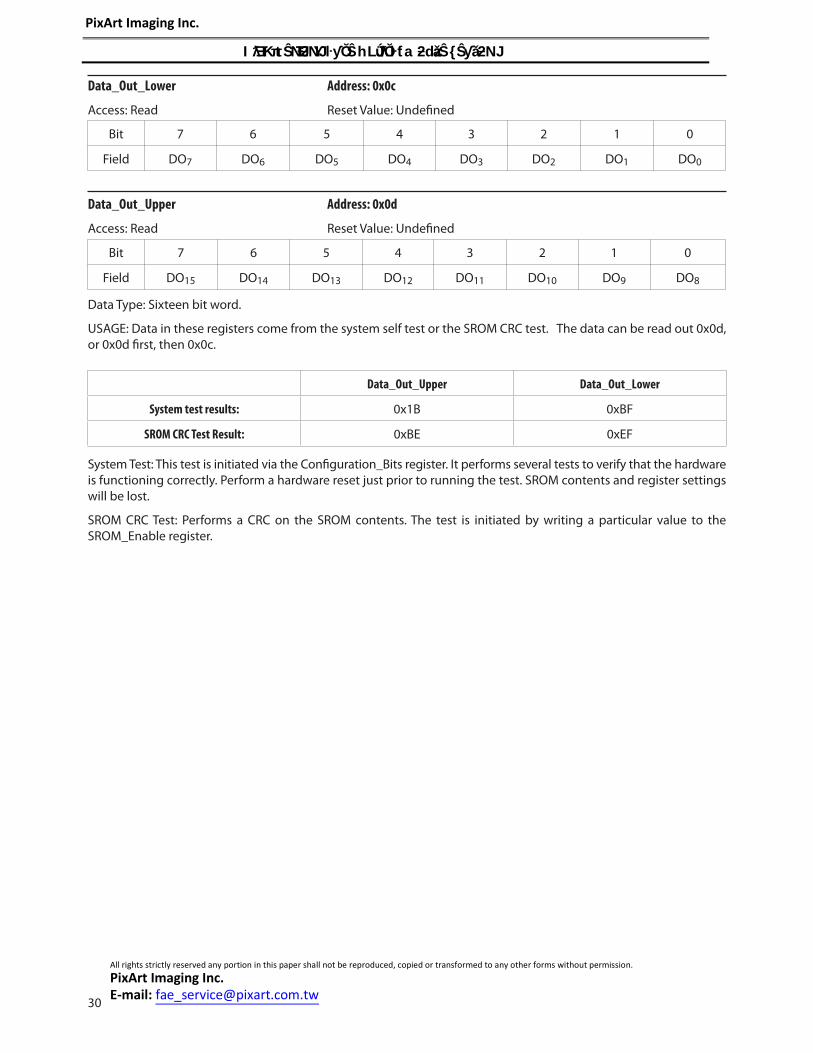
System Test: This test is initiated via the Confi guration_Bits register. It performs several tests to verify that the hardware is functioning correctly. Perform a hardware reset just prior to running the test. SROM contents and register settings will be lost.
SROM CRC Test: Performs a CRC on the SROM contents. The test is initiated by writing a particular value to the SROM_Enable register.
Bit 7 6 5 4 3 2 1 0
Field DO7 DO6 DO5 DO4 DO3 DO2 DO1 DO0
Bit 7 6 5 4 3 2 1 0
Field DO15 DO14 DO13 DO12 DO11 DO10 DO9 DO8
Data_Out_Upper Data_Out_Lower
System test results: 0x1B 0xBF
SROM CRC Test Result: 0xBE 0xEF
Data_Out_Lower Address: 0x0c
Access: Read Reset Value: Undefi ned
Data_Out_Upper Address: 0x0d
Access: Read Reset Value: Undefi ned
Data Type: Sixteen bit word.
USAGE: Data in these registers come from the system self test or the SROM CRC test. The data can be read out 0x0d, or 0x0d fi rst, then 0x0c.
All rights strictly reserved any portion in this paper shall not be reproduced, copied or transformed to any other forms without permission.
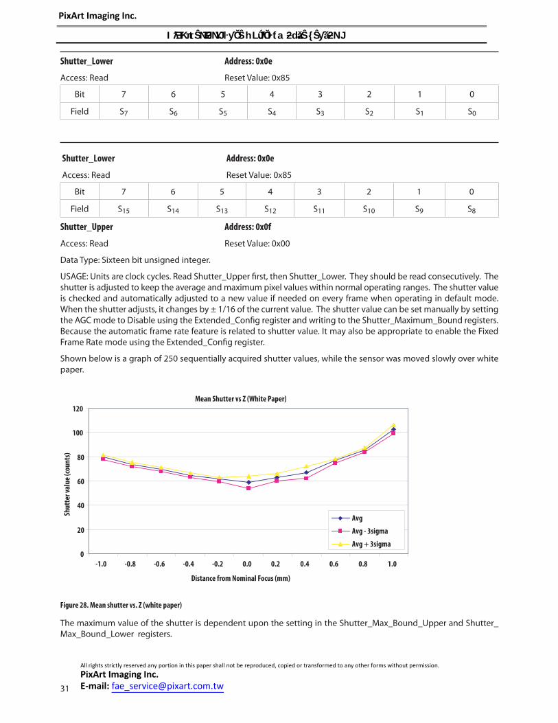
The maximum value of the shutter is dependent upon the setting in the Shutter_Max_Bound_Upper and Shutter_Max_Bound_Lower registers.
Shutter_Lower Address: 0x0e
Access: Read Reset Value: 0x85
Shutter_Upper Address: 0x0f
Access: Read Reset Value: 0x00
Data Type: Sixteen bit unsigned integer.
USAGE: Units are clock cycles. Read Shutter_Upper fi rst, then Shutter_Lower. They should be read consecutively. The shutter is adjusted to keep the average and maximum pixel values within normal operating ranges. The shutter value is checked and automatically adjusted to a new value if needed on every frame when operating in default mode. When the shutter adjusts, it changes by ± 1/16 of the current value. The shutter value can be set manually by setting the AGC mode to Disable using the Extended_Confi g register and writing to the Shutter_Maximum_Bound registers. Because the automatic frame rate feature is related to shutter value. It may also be appropriate to enable the Fixed Frame Rate mode using the Extended_Confi g register.
Shown below is a graph of 250 sequentially acquired shutter values, while the sensor was moved slowly over white paper.
Bit 7 6 5 4 3 2 1 0
Field S15 S14 S13 S12 S11 S10 S9 S8
Shutter_Lower Address: 0x0e
Access: Read Reset Value: 0x85
Bit 7 6 5 4 3 2 1 0
Field S7 S6 S5 S4 S3 S2 S1 S0
Mean Shutter vs Z (White Paper)
Distance from Nominal Focus (mm)
Shu
tter
val
ue
(cou
nts
)
0
20
40
60
80
100
120
-1.0 -0.8 -0.6 -0.4 -0.2 0.0 0.2 0.4 0.6 0.8 1.0
Avg
Avg - 3sigma
Avg + 3sigma
All rights strictly reserved any portion in this paper shall not be reproduced, copied or transformed to any other forms without permission.
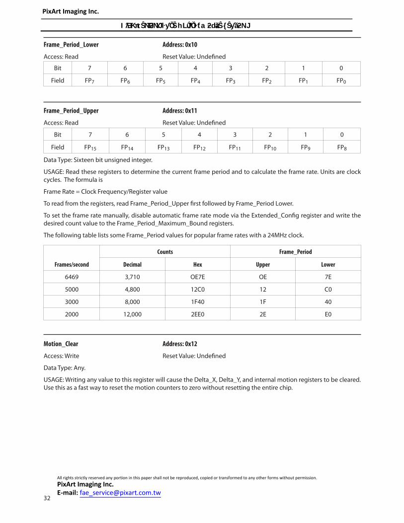
USAGE: Writing any value to this register will cause the Delta_X, Delta_Y, and internal motion registers to be cleared. Use this as a fast way to reset the motion counters to zero without resetting the entire chip.
Data Type: Sixteen bit unsigned integer.
USAGE: Read these registers to determine the current frame period and to calculate the frame rate. Units are clock cycles. The formula is
Frame Rate = Clock Frequency/Register value
To read from the registers, read Frame_Period_Upper fi rst followed by Frame_Period Lower.
To set the frame rate manually, disable automatic frame rate mode via the Extended_Confi g register and write the desired count value to the Frame_Period_Maximum_Bound registers.
The following table lists some Frame_Period values for popular frame rates with a 24MHz clock.
Bit 7 6 5 4 3 2 1 0
Field FP7 FP6 FP5 FP4 FP3 FP2 FP1 FP0
Bit 7 6 5 4 3 2 1 0
Field FP15 FP14 FP13 FP12 FP11 FP10 FP9 FP8
Frames/second
Counts Frame_Period
Decimal Hex Upper Lower
6469 3,710 OE7E OE 7E
5000 4,800 12C0 12 C0
3000 8,000 1F40 1F 40
2000 12,000 2EE0 2E E0
All rights strictly reserved any portion in this paper shall not be reproduced, copied or transformed to any other forms without permission.
USAGE: Writing 0x83 to this register will cause the next available complete 1 2/3 frames of pixel values to be stored to SROM RAM. Writing to this register is required before using the Frame Capture burst mode to read the pixel values (see the Synchronous Serial Port section for more details). Writing to this register will stop navigation and cause any fi rmware loaded in the SROM to be overwritten. A hardware reset is required to restore navigation, and the fi rmware must be reloaded using the SROM Download burst method.
This register can also be used to read the frame capture data. The same data available by reading the Pixel_Burst register using burst mode is available by reading this register in the normal fashion. The data pointer is automatically incremented after each read so all 1536 pixel values (1 and 2/3 frames) may be obtained by reading this register 1536 times in a row. Both methods share the same pointer such that reading pixel values from this register will increment the pointer causing subsequent reads from the Pixel_Burst register (without initiating a new frame dump) to start at the current pointer location. This register will return all zeros if read before the frame capture data is ready. See the Frame Capture description in the Synchronous Serial Port section for more information.
This register will not retain the last value written. Reads will return zero or frame capture data.
Data Type: 8-bit number.
USAGE: Write to this register to start either SROM download or SROM CRC test.
Write 0x18 to this register before downloading SROM fi rmware to the SROM_Load register. The download will not be successful unless this register contains the correct value.
Write 0xA1 to start the SROM CRC test. Wait 7ms plus one frame period , then read result from the Data_Out_Lower and Data_Out_Upper registers. Navigation is halted and the SPI port should not be used during this test.
Bit 7 6 5 4 3 2 1 0
Field FC7 FC6 FC5 FC4 FC3 FC2 FC1 FC0
Bit 7 6 5 4 3 2 1 0
Field SE7 SE6 SE5 SE4 SE3 SE2 SE1 SE0
Reserved Address: 0x15 – 0x18
All rights strictly reserved any portion in this paper shall not be reproduced, copied or transformed to any other forms without permission.
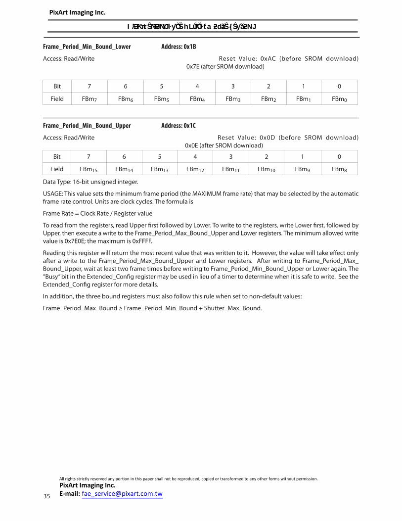
Field FBm15 FBm14 FBm13 FBm12 FBm11 FBm10 FBm9 FBm8
Frame_Period_Max_Bound_Lower Address: 0x19
Access: Read/Write Reset Value: 0xE0
Frame_Period_Max_Bound_Upper Address: 0x1A
Access: Read/Write Reset Value: 0x2E
Data Type: 16-bit unsigned integer.
USAGE: This value sets the maximum frame period (the MINIMUM frame rate) which may be selected by the automatic frame rate control, or sets the actual frame period when operating in manual mode. Units are clock cycles. The formula is
Frame Rate = Clock Frequency / Register value
To read from the registers, read Upper fi rst followed by Lower. To write to the registers, write Lower fi rst, followed by Upper. To set the frame rate manually, disable automatic frame rate mode via the Extended_Confi g register and write the desired count value to these registers.
Writing to the Frame_Period_Max_Bound_Upper and Lower registers also activates any new values in the following registers:
• Frame_Period_Max_Bound_Upper and Lower
• Frame_Period_Min_Bound_Upper and Lower
• Shutter_Max_Bound_Upper and Lower
Any data written to these registers will be saved but will not take eff ect until the write to the Frame_Period_Max_Bound_Upper and Lower is complete. After writing to this register, two complete frame times are required to implement the new settings. Writing to any of the above registers before the implementation is complete may put the chip into an undefi ned state requiring a reset. The “Busy” bit in the Extended_Confi g register may be used in lieu of a timer to determine when it is safe to write. See the Extended_Confi g register for more details.
The following table lists some Frame_Period values for popular frame rates (clock rate = 24MHz).
In addition, the three bound registers must also follow this rule when set to non-default values:
USAGE: This value sets the minimum frame period (the MAXIMUM frame rate) that may be selected by the automatic frame rate control. Units are clock cycles. The formula is
Frame Rate = Clock Rate / Register value
To read from the registers, read Upper fi rst followed by Lower. To write to the registers, write Lower fi rst, followed by Upper, then execute a write to the Frame_Period_Max_Bound_Upper and Lower registers. The minimum allowed write value is 0x7E0E; the maximum is 0xFFFF.
Reading this register will return the most recent value that was written to it. However, the value will take eff ect only after a write to the Frame_Period_Max_Bound_Upper and Lower registers. After writing to Frame_Period_Max_Bound_Upper, wait at least two frame times before writing to Frame_Period_Min_Bound_Upper or Lower again. The “Busy” bit in the Extended_Confi g register may be used in lieu of a timer to determine when it is safe to write. See the Extended_Confi g register for more details.
In addition, the three bound registers must also follow this rule when set to non-default values:
USAGE: This value sets the maximum allowable shutter value when operating in automatic mode. Units are clock cycles. Since the automatic frame rate function is based on shutter value, the value in these registers can limit the range of the frame rate control. To read from the registers, read Upper fi rst followed by Lower. To write to the registers, write Lower fi rst, followed by Upper, then execute a write to the Frame_Period_Max_Bound_Upper and Lower registers. To set the shutter manually, disable the AGC via the Extended_Confi g register and write the desired value to these registers.
Reading this register will return the most recent value that was written to it. However, the value will take eff ect only after a write to the Frame_Period_Max_Bound_Upper and Lower registers. After writing to Frame_Period_Max_Bound_Upper, wait at least two frame times before writing to Shutter_Max_Bound_Upper or Lower again. The “Busy” bit in the Extended_Confi g register may be used in lieu of a timer to determine when it is safe to write. See the Extended_Confi g register for more details.
In addition, the three bound registers must also follow this rule when set to non-default values:
USAGE: Contains the revision of the downloaded Shadow ROM fi rmware. If the fi rmware has been successfully down-loaded and the chip is operating out of SROM, this register will contain the SROM fi rmware revision, otherwise it will contain 0x00.
Note: The IC hardware revision is available by reading the Revision_ID register (register 0x01).
Reserved Address: 0x20 – 0x3C
All rights strictly reserved any portion in this paper shall not be reproduced, copied or transformed to any other forms without permission.
Field OB7 Reserved OB5 Reserved Reserved Reserved OB1 OB0
Field Name Description
OB7 If set, chip is running SROM code
Reserved Reserved
OB5 NPD pulse was detected
Reserved Reserved
Reserved Reserved
Reserved Reserved
OB1 Set once per frame
OB0 Set once per frame
Bit 7 6 5 4 3 2 1 0
Field NPID7 NPID6 NPID5 NPID4 NPID3 NPID2 NPID1 NPID0
Reserved Address: 0x3E
Inverse_Product_ID Address: 0x3F
Access: Read Reset Value: 0xF8
Data Type: Bit fi eld
USAGE: Each bit is set by some process or action at regular intervals, or when the event occurs. The user must clear the register by writing 0x00, wait an appropriate delay, and read the register. The active processes will have set their corresponding bit(s). This register may be used as part of a recovery scheme to detect a problem caused by EFT/B or ESD.
Data Type: Inverse 8-Bit unsigned integer
USAGE: This value is the inverse of the Product_ID, located at the inverse address. It can be used to test the SPI port.
Pixel_Burst Address: 0x40
Access: Read Reset Value: 0x00
Data Type: Eight bit unsigned integer
USAGE: The Pixel_Burst register is used for high-speed access to all the pixel values from one and 2/3 complete frame. See the Synchronous Serial Port section for use details.
Bit 7 6 5 4 3 2 1 0
Field PB7 PB6 PB5 PB4 PB3 PB2 PB1 PB0
All rights strictly reserved any portion in this paper shall not be reproduced, copied or transformed to any other forms without permission.
USAGE: The Motion_Burst register is used for high-speed access to the Motion, Delta_X, and Delta_Y, SQUAL, Shutter_Upper, and Shutter_Lower and Maximum_Pixel registers. See the Synchronous Serial Port section for use details.
Motion_Burst Address: 0x50
Access: Read Reset Value: 0x00
SROM_Load Address: 0x 60
Access: Write Rset Value: N/A
Data Type: Eight bit unsigned integer
USAGE: The SROM_Load register is used for high-speed programming of the ADNS-3080 from an external SROM or microcontroller. See the Synchronous Serial Port section for use details.
All rights strictly reserved any portion in this paper shall not be reproduced, copied or transformed to any other forms without permission.