AV Series APISSYS OpenVPX AV 1 1 9 Wideband Transceiver with DDC Radar - MIMO 3U VPX, Virtex 7 FPGA Dual RF in – dual RF out, 1 GHz instantaneous bandwidth, 4.5 GHz total bandwidth Conduction or Air-Cooled
Transcript
AV Series
APISSYS OpenVPX
AV 119Wideband Transceiver with DDC
Radar - MIMO
3U VPX, Virtex 7 FPGADual RF in – dual RF out, 1 GHz instantaneous bandwidth,4.5 GHz total bandwidthConduction or Air-Cooled
AV 119
12-bit 2.5 Gsps Analog-Digital Converters
The AV119 Analog to Digital conversion is
performed by two 12-bit 2.5 Gsps ADCs with
independent 120 or 240 MHz Digital Down
Converters.
The AV119 provides two front panel SMPM
connectors for analog inputs.
Single ended input signals are AC coupled
with an input bandwidth from 1 MHz to more
than 5.5 GHz with 9 dBm input level.
16-bit 2.5 Gsps Digital-AnalogConverters
The AV119 Digital to Analog conversion is per-
formed by a Quad 16-bit 2.5 Gsps DACs with
independent Digital UP Converters.
Two I/Q modulators with more than 1 GHz
instantaneous bandwidth allow generation of
RF signals from 300 MHz up to 4.5 GHz.
The AV119 provides two front panel SMPM
connectors for analog RF outputs.
A loopback mode between RF out and ADC
input is provided for on board calibration.
Clock
The AV119 provides four independent ultra-
low jitter clock synthesizers locked on a 100
MHz internal reference.
The AV119 provides a front panel SMPM
connector for external reference input, 10
to 100 MHz as well as a VPX P2 input. A
reference output is available on a front panel
SMPM connector and on VPX P2.
Three SMPM connectors support either ex-
ternal clock inputs-outputs for the ADCs and
the quad DAC. External clock from 500 MHz
to 2.5 GHz are supported.
An SMPM connector supports an external LO
for the IQ modulators
OverviewThe AV119 is part of ApisSys’ range of High Speed data conversion and signal processing solu-
tions based on the VITA 46, VPX standard.
The AV119 is fully compliant with the OpenVPX standard, accommodating various communication
protocols such as PCIe, SRIO, 1 Gbit and XAUI 10 Gbit Ethernet, as well as non OpenVPX adopted
standard such as Aurora.
The AV119 combines two 12-bit 2.5 Gsps ADCs plus 2 RF out built on 16-bit 2.5 Gsps I/Q DAC
and RF modulators with ultra-high processing power delivered by Xilinx® Virtex® 7 FPGA, making
it ideally suited for fully synchronous multiple channels test and measurement, Electronic Warfare,
Ultra Wideband Radar Transceivers or MIMO applications.
The AV119 features an internal ultra-low jitter reference and four independent clock synthesizers
The AV119 supports an external trigger signal coupled with a 15ps resolution Time to Digital
Converter (TDC).
The AV119 includes one Xilinx® Virtex® 7 FPGA VX415T or VX690T for an impressive processing
capability of more than 2 TMACs (Multiply Accumulate per second), one high speed 256M64
DDR3 SDRAM memory for data processing and a 1 Gb synchronous FLASH memory for multiple
The AV119 provides a USB 2.0 interface and a 10/100 Ethernet interface intended to be used for
system monitoring and supervision.
The AV119 comes with complete software drivers for Windows and Linux. An FPGA Development
Kit is provided including all necessary cores to build user FPGA application.
Applications Wideband Radar transceiver
Electronic Warfare, COMINT
Instrumentation
MIMO
Features 2 channels 2.5 Gsps 12-bit ADC
2 independent Digital Down Converters,
120 or 140 MHz BW.
2 RF out, 16-bit 2.5 Gsps I/Q DAC with
Digital Up Converter and RF modulators
4 independent Low jitter clock
synthesizers and LO
External and internal reference
User programmable Xilinx® Virtex® 7
VX415T or VX690T FPGA
667 MHz 256M64 DDR3 SDRAM
3U OpenVPX standard compliant
Air cooled and Conduction cooled
rugged versions
synthesizer allow for accurate adjustment of
phase delay between all channels.
FPGA
VX415T or VX690T user programmable
FPGA. Only few resources are used to control
and communicate with external hardware
such as DDR3 SDRAM and monitoring sub-
system, leaving most of the logic and block
RAM and all DSP resources available for cus-
tomer processing.
Dedicated to signal processing, the Xilinx Vir-
tex 7 VX415T FPGA includes 412,160 logics
cells, 880 bloc RAM (36 Kbit each), 2,160
DSP48E1 slices and 2 PCIe interface blocs.
The most powerful version embeds a Xilinx
Virtex 7 VX690T which provides 693,120
logics cells, 1,470 bloc RAM and 3,600
DSP48E1 slices for an impressive processing
power of more than 2 TMACs.
The FPGA is delivered in -2 speed grade.
Memories
The AV119 includes one 667 MHz 256M64
DDR3 SDRAM memory bank and one 1 Gbit
synchronous BPI FLASH used to store mul-
VPX interface
The AV119 features an OpenVPX VITA 65
compliant interface with support for two Fat
Pipes for Data Plane, one Fat Pipe for Expan-
sion Plane, two Ultra Thin Pipes for Control
on P1. The AV119 also supports 24 LVDS dif-
ferential pairs on P2 plus USB2.0 and 10/100
Ethernet for supervision and monitoring.
The AV119 features two low phase noise
clock generators able to synthesize clock re-
ferences for the FPGA GTXs from 100 MHz to
312.5 MHz, allowing support of all major pro-
tocols such as Aurora, GigE, PCIe Gen 1 and
Gen 2, SATA, SRIO and XAUI 10Gbit Ethernet
up to 12.5 Gbps.
Microcontroller
The AV119 features a 32-bit 80 MHz micro-
controller used primarily for board monitoring
and supervision.
The microcontroller supports a USB 2.0 and
a 10/100 Ethernet interfaces accessible on
the VPX P2 user IO pins through an ApisSys
AR102 Rear Transition Module or an ANSI/
VITA 46.10 compliant custom RTM board.
necessary features for board monitoring and
supervision.
Firmware
which includes VHDL cores allowing for
control and communication with all AV119
hardware resources.
A base design is provided which demons-
trates the use of the AV119 and gives users a
Xilinx VIVADO® 2014.4 design suite and later.
Software
The AV119 is delivered with software drivers
for Windows 7 and Linux.
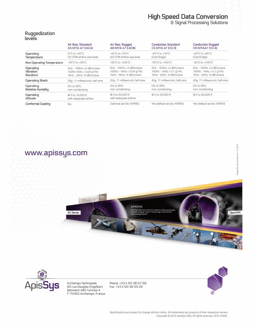
Ruggedization
The AV119 is delivered in air cooled and
conduction cooled standard or rugged ver-
sions for use in severe environmental condi-
tions. Standard VITA 47 supported ruggediza-
tion levels are EAC4, EAC6, ECC3 and ECC4.
I2C
VPX power rails
10/100 Eth
USB
DP01
DP02
Fat Pipe x1
2x Ultra-thin Pipes
2x Ultra-thin Pipes
LVDS pairs
Ultra lownoise reference
I
Q
I
Q
TRG
Ref In
In0
In1
Out0
Out1
Trg
1 Gb BPI Flash
256M64 667MHz DDR3 SDRAM
VIRTEX 7FPGA
VX415TVX690T-2FFG1158I
Power SuppyDC/DC
µControllerMonitoring
P1
P2
P0
Reference Distribution
IQModulator
IQModulator
Clock Synthesizer
Optional
DDCADC
Clock Synthesizer
Optional
DDCADC
Optional
DUCDAC
Optional
DUCDAC
Optional
DUCDAC
Clock Synthesizer
Optional
DUCDAC
AV Series
APISSYS OpenVPX
Specifications
Analog Inputs-Outputs Input - Output coupling: AC
Input Full power bandwidth: > 5.5 GHz Full scale : 10 dBm Output bandwidth: > 4.5 GHz
Impedance: 50 Ohm, SMPM
Analog-Digital Conversion
Resolution: 12 bit Sampling Performances @1 GHz
SNR: 58.5 dBFS SFDR: 69 dBc ENOB: 9.3 bits
Digital-Analog Conversion
RF IQ modulator instantaneous BW: > 1 GHz
SFDR: 55 dBc on 1 GHz bandwidth
Clock Internal :
Four independent synthesizers, 1 GHz to 2.5 GHz low jitter clock ADC
and DAC 400 MHz to 4.1 GHz LO
External Input/Output Clocks: frequency: 1 GHz to 2.5 GHz for ADC
and DAC 400 MHz to 4.1 GHz LO input
External reference: frequency: 10 MHz to 100 MHz Connector: SMPM, 50 Ohm and VPX P2
Digital Up and Down Converter Independent DDC on ADC:
Tuning frequency step: 10-bit NCO
Independent DUC on DAC: Tuning frequency step: 48-bit NCO DUC with x1 to x16 interpolation.
Trigger External: LVDS or LVPECL
VPX P2
FPGA FPGA: Xilinx Virtex 7
XC7VX415T-2FFG1158 or XC7VX690T-2FFG1158
Memory 1 bank 256M64 DDR3 SDRAM,
667 MHz clock One 1 Gbit NOR FLASH memory
VPX interface P1:
Data plane: two fat pipes Expansion plane: one fat pipe Control plane: 2 ultra-thin pipes
P2: USB2.0 and 10/100 Ethernet
Software support Software Drivers:
Windows 7 Linux
Application example: Windows and Linux
Firmware support VHDL cores for all hardware resources Base design Supported by Xilinx VIVADO 2014.4
and later
Ruggedization As per VITA 47:
Air cooled : EAC4 and EAC6 Conduction cooled : ECC3 and ECC4
Power dissipation (690T) +12V: 6.2 A max (75W) TBC +5V: 8.0 A max (40W) TBC +3.3V: 0.5 A max (1.6W) TBC +3.3VAUX: 0.3 A max (1.1W) TBC