32072AS–AVR32–03/09 Features • High Performance, Low Power AVR ® 32 UC 32-Bit Microcontroller – Compact Single-Cycle RISC Instruction Set Including DSP Instruction Set – Read-Modify-Write Instructions and Atomic Bit Manipulation – Performing 1.49DMIPS/MHz • Up to 91DMIPS Running at 66MHz from Flash (1 Wait-State) • Up to 54 DMIPS Running at 36MHz from Flash (0 Wait-State) – Memory Protection Unit • Multi-Layer Bus System – High-Performance Data Transfers on Separate Buses for Increased Performance – 8 Peripheral DMA Channels (PDCA) Improves Speed for Peripheral Communication – 4 generic DMA Channels for High Bandwidth Data Paths • Internal High-Speed Flash – 256KBytes, 128KBytes, 64KBytes versions – Single-Cycle Flash Access up to 36MHz – Prefetch Buffer Optimizing Instruction Execution at Maximum Speed – 4 ms Page Programming Time and 8ms Full-Chip Erase Time – 100,000 Write Cycles, 15-year Data Retention Capability – Flash Security Locks and User Defined Configuration Area • Internal High-Speed SRAM – 64KBytes Single-Cycle Access at Full Speed, Connected to CPU Local Bus – 64KBytes on the Multi-Layer Bus System • Interrupt Controller – Autovectored Low Latency Interrupt Service with Programmable Priority • System Functions – Power and Clock Manager Including Internal RC Clock and One 32KHz Oscillator – Two Multipurpose Oscillators and Two Phase-Lock-Loop (PLL), – Watchdog Timer, Real-Time Clock Timer • External Memories – Support SDRAM, SRAM, NandFlash (1-bit and 4-bit ECC), Compact Flash – Up to 66 MHz • External Storage device support – MultiMediaCard (MMC), Secure-Digital (SD), SDIO V1.1 – CE-ATA, FastSD, SmartMedia, Compact Flash – Memory Stick: Standard Format V1.40, PRO Format V1.00, Micro – IDE Interface • One Advanced Encryption System (AES) for AT32UC3A3256S, AT32UC3A3128S and AT32UC3A364S – 256-, 192-, 128-bit Key Algorithm, Compliant with FIPS PUB 197 Specifications – Buffer Encryption/Decryption Capabilities • Universal Serial Bus (USB) – High-Speed USB (480Mbit/s) Device/MiniHost with On-The-Go (OTG) – Flexible End-Point Configuration and Management with Dedicated DMA Channels – On-Chip Transceivers Including Pull-Ups • One 8-channel 10-bit Analog-To-Digital Converter, multiplexed with Digital IOs. • Two Three-Channel 16-bit Timer/Counter (TC) • Four Universal Synchronous/Asynchronous Receiver/Transmitters (USART) – Independent Baudrate Generator, Support for SPI, IrDA and ISO7816 interfaces AVR ® 32 32-Bit Microcontroller AT32UC3A3256S AT32UC3A3256 AT32UC3A3128S AT32UC3A3128 AT32UC3A364S AT32UC3A364 Summary Preliminary
Transcript
32072AS–AVR32–03/09
Features• High Performance, Low Power AVR®32 UC 32-Bit Microcontroller
– Compact Single-Cycle RISC Instruction Set Including DSP Instruction Set– Read-Modify-Write Instructions and Atomic Bit Manipulation– Performing 1.49DMIPS/MHz
• Up to 91DMIPS Running at 66MHz from Flash (1 Wait-State)• Up to 54 DMIPS Running at 36MHz from Flash (0 Wait-State)
– Memory Protection Unit• Multi-Layer Bus System
– High-Performance Data Transfers on Separate Buses for Increased Performance– 8 Peripheral DMA Channels (PDCA) Improves Speed for Peripheral
Communication– 4 generic DMA Channels for High Bandwidth Data Paths
• Internal High-Speed Flash– 256KBytes, 128KBytes, 64KBytes versions– Single-Cycle Flash Access up to 36MHz – Prefetch Buffer Optimizing Instruction Execution at Maximum Speed– 4 ms Page Programming Time and 8ms Full-Chip Erase Time– 100,000 Write Cycles, 15-year Data Retention Capability– Flash Security Locks and User Defined Configuration Area
• Internal High-Speed SRAM– 64KBytes Single-Cycle Access at Full Speed, Connected to CPU Local Bus– 64KBytes on the Multi-Layer Bus System
• Interrupt Controller– Autovectored Low Latency Interrupt Service with Programmable Priority
• System Functions– Power and Clock Manager Including Internal RC Clock and One 32KHz Oscillator– Two Multipurpose Oscillators and Two Phase-Lock-Loop (PLL), – Watchdog Timer, Real-Time Clock Timer
• External Memories– Support SDRAM, SRAM, NandFlash (1-bit and 4-bit ECC), Compact Flash– Up to 66 MHz
• External Storage device support– MultiMediaCard (MMC), Secure-Digital (SD), SDIO V1.1– CE-ATA, FastSD, SmartMedia, Compact Flash– Memory Stick: Standard Format V1.40, PRO Format V1.00, Micro– IDE Interface
• One Advanced Encryption System (AES) for AT32UC3A3256S, AT32UC3A3128Sand AT32UC3A364S
– 256-, 192-, 128-bit Key Algorithm, Compliant with FIPS PUB 197 Specifications– Buffer Encryption/Decryption Capabilities
• Universal Serial Bus (USB)– High-Speed USB (480Mbit/s) Device/MiniHost with On-The-Go (OTG)– Flexible End-Point Configuration and Management with Dedicated DMA Channels– On-Chip Transceivers Including Pull-Ups
• One 8-channel 10-bit Analog-To-Digital Converter, multiplexed with Digital IOs.• Two Three-Channel 16-bit Timer/Counter (TC)• Four Universal Synchronous/Asynchronous Receiver/Transmitters (USART)
– Independent Baudrate Generator, Support for SPI, IrDA and ISO7816 interfaces
– Support for Hardware Handshaking, RS485 Interfaces and Modem Line• Two Master/Slave Serial Peripheral Interfaces (SPI) with Chip Select Signals• One Synchronous Serial Protocol Controller
– Supports I2S and Generic Frame-Based Protocols• Two Master/Slave Two-Wire Interface (TWI), 400kbit/s I2C-compatible• On-Chip Debug System (JTAG interface)
– Nexus Class 2+, Runtime Control, Non-Intrusive Data and Program Trace• 110 General Purpose Input/Output (GPIOs)
– Standard or High Speed mode– Toggle capability: up to 66MHz
• 144-pin TBGA and LQFP• Single 3.3V Power Supply
332072AS–AVR32–03/09
AT32UC3A3
1. DescriptionThe AT32UC3A3 is a complete System-On-Chip microcontroller based on the AVR32 UC RISCprocessor running at frequencies up to 66MHz. AVR32 UC is a high-performance 32-bit RISCmicroprocessor core, designed for cost-sensitive embedded applications, with particular empha-sis on low power consumption, high code density and high performance.
The processor implements a Memory Protection Unit (MPU) and a fast and flexible interrupt con-troller for supporting modern operating systems and real-time operating systems. Highercomputation capabilities are achievable using a rich set of DSP instructions.
The AT32UC3A3 incorporates on-chip Flash and SRAM memories for secure and fast access.
The Peripheral Direct Memory Access Controller (PDCA) enables data transfers betweenperipherals and memories without processor involvement. The PDCA drastically reduces pro-cessing overhead when transferring continuous and large data streams.
The Direct Memory Access controller (DMACA) allows high bandwidth data flows between highspeed peripherals (USB, External Memories, MMC, SDIO, ...) and through high speed internalfeatures (AES, internal memories).
The Power Manager improves design flexibility and security: the on-chip Brown-Out Detectormonitors the power supply, the CPU runs from the on-chip RC oscillator or from one of externaloscillator sources, a Real-Time Clock and its associated timer keeps track of the time.
The Device includes two sets of three identical 16-bit Timer/Counter (TC) channels. Each chan-nel can be independently programmed to perform frequency measurement, event counting,interval measurement, pulse generation, delay timing and pulse width modulation. 16-bit chan-nels are combined to operate as 32-bit channels.
The AT32UC3A3 also features many communication interfaces for communication intensiveapplications like UART, SPI or TWI. Additionally, a flexible Synchronous Serial Controller (SSC)and an USB are available.
The SSC provides easy access to serial communication protocols and audio standards like I2S.
The High-Speed (480MBit/s) USB 2.0 Device interface supports several USB Classes at thesame time thanks to the rich Endpoint configuration. The On-The-Go (OTG) Host interfaceallows device like a USB Flash disk or a USB printer to be directly connected to the processor.
AT32UC3A3 integrates a class 2+ Nexus 2.0 On-Chip Debug (OCD) System, with non-intrusivereal-time trace, full-speed read/write memory access in addition to basic runtime control.
– 15 general-purpose 32-bit registers– 32-bit Stack Pointer, Program Counter and Link Register reside in register file– Fully orthogonal instruction set– Privileged and unprivileged modes enabling efficient and secure Operating Systems– Innovative instruction set together with variable instruction length ensuring industry leading
code density– DSP extension with saturating arithmetic, and a wide variety of multiply instructions
• Three stage pipeline allows one instruction per clock cycle for most instructions– Byte, halfword, word and double word memory access– Multiple interrupt priority levels
• MPU allows for operating systems with memory protection
2.1.2 Debug and Test System• IEEE1149.1 compliant JTAG and boundary scan• Direct memory access and programming capabilities through JTAG interface• Extensive On-Chip Debug features in compliance with IEEE-ISTO 5001-2003 (Nexus 2.0) Class 2+
– Low-cost NanoTrace supported• Auxiliary port for high-speed trace information• Hardware support for six Program and two data breakpoints• Unlimited number of software breakpoints supported• Advanced Program, Data, Ownership and Watchpoint trace supported
2.1.3 Peripheral DMA Controller• Transfers from/to peripheral to/from any memory space without intervention of the processor• Next Pointer Support, forbids strong real-time constraints on buffer management• Eight channels and 24 Handshake interfaces
– Two for each USART– Two for each Serial Synchronous Controller (SSC)– Two for each Serial Peripheral Interface (SPI)– One for ADC– Four for each TWI Interface– Two for each Audio Bit Stream DAC
2.1.4 Bus System• High Speed Bus (HSB) matrix with 7 Masters and 10 Slaves handled
– Handles Requests from• Masters: the CPU (Instruction and Data Fetch), PDCA, CPU SAB, USBB, DMACA• Slaves: the internal Flash, internal SRAM, Peripheral Bus A, Peripheral Bus B, External
Bus Interface (EBI), Advanced Encrytion Standard (AES)– Round-Robin Arbitration (three modes supported: no default master, last accessed default
master, fixed default master)– Burst breaking with Slot Cycle Limit– One address decoder provided per master
• Peripheral Bus A able to run on at divided bus speeds compared to the High Speed Bus
632072AS–AVR32–03/09
AT32UC3A3
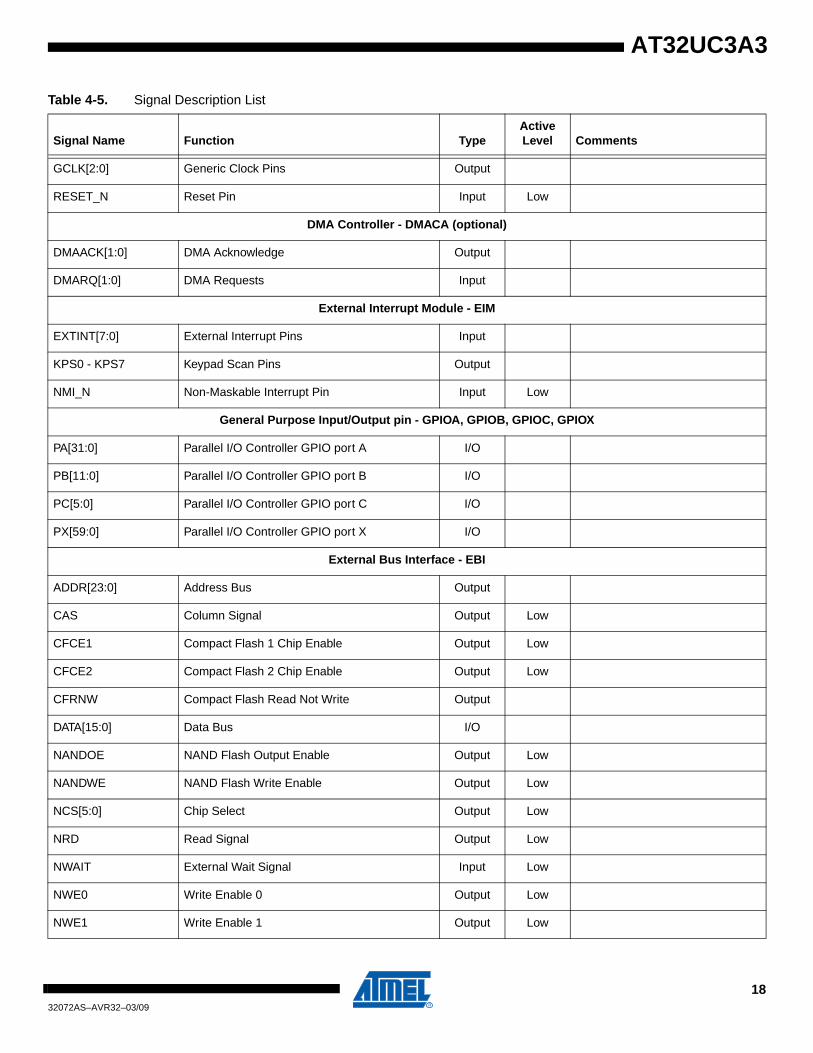
3. Signals DescriptionThe following table gives details on the signal name classified by peripheral
Table 3-1. Signal Description List
Signal Name Function TypeActive Level Comments
Power
VDDIO I/O Power Supply Power 3.0 to 3.6 V
VDDANA Analog Power Supply Power 3.0 to 3.6 V
VDDIN Voltage Regulator Input Supply Power 2.7 to 3.6 V
ONREG Voltage Regulator ON/OFFPower Control
1 2.7 to 3.6 V
VDDCORE Voltage Regulator Output for Digital SupplyPower Output
1.65 to 1.95V
GNDANA Analog Ground Ground
GNDIO I/O Ground Ground
GNDCORE DIgital Ground Ground
GNDPLL PLL Ground Ground
Clocks, Oscillators, and PLL’s
XIN0, XIN1, XIN32 Crystal 0, 1, 32 Input Analog
XOUT0, XOUT1, XOUT32
Crystal 0, 1, 32 Output Analog
JTAG
TCK Test Clock Input
TDI Test Data In Input
TDO Test Data Out Output
TMS Test Mode Select Input
Auxiliary Port - AUX
MCKO Trace Data Output Clock Output
MDO[5:0] Trace Data Output Output
MSEO[1:0] Trace Frame Control Output
EVTI_N Event In Output Low
EVTO_N Event Out Output Low
Power Manager - PM
732072AS–AVR32–03/09
AT32UC3A3
GCLK[2:0] Generic Clock Pins Output
RESET_N Reset Pin Input Low
DMA Controller - DMACA (optional)
DMAACK[1:0] DMA Acknowledge Output
DMARQ[1:0] DMA Requests Input
External Interrupt Module - EIM
EXTINT[7:0] External Interrupt Pins Input
KPS0 - KPS7 Keypad Scan Pins Output
NMI_N Non-Maskable Interrupt Pin Input Low
General Purpose Input/Output pin - GPIOA, GPIOB, GPIOC, GPIOX
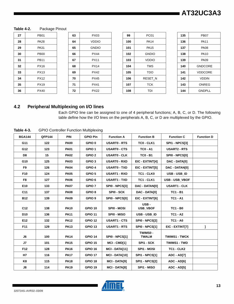
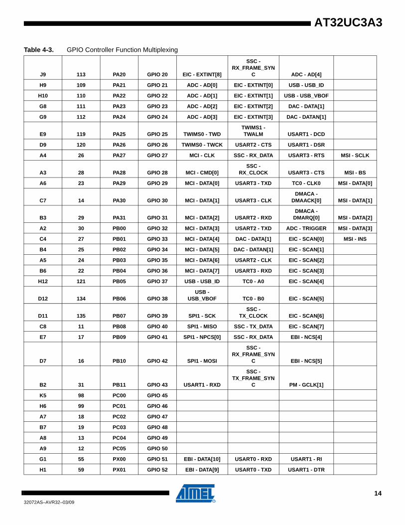
4.2 Peripheral Multiplexing on I/O linesEach GPIO line can be assigned to one of 4 peripheral functions; A, B, C, or D. The followingtable define how the I/O lines on the peripherals A, B, C, or D are multiplexed by the GPIO.
27 PB01 63 PX03 99 PC01 135 PB07
28 PA28 64 VDDIO 100 PA14 136 PA11
29 PA31 65 GNDIO 101 PA15 137 PA08
30 PB00 66 PX44 102 GNDIO 138 PA10
31 PB11 67 PX11 103 VDDIO 139 PA09
32 PX16 68 PX14 104 TMS 140 GNDCORE
33 PX13 69 PX42 105 TDO 141 VDDCORE
34 PX12 70 PX45 106 RESET_N 142 VDDIN
35 PX19 71 PX41 107 TCK 143 ONREG
36 PX40 72 PX22 108 TDI 144 GNDPLL
Table 4-2. Package Pinout
Table 4-3. GPIO Controller Function Multiplexing
BGA144 QFP144 PIN GPIO Pin Function A Function B Function C Function D
4.3.1 JTAG PinsTMS and TDI pins have pull-up resistors. TDO pin is an output, driven at up to VDDIO, and hasno pull-up resistor.
4.3.2 RESET_N PinThe RESET_N pin is a schmitt input and integrates a permanent pull-up resistor to VDDIO. Asthe product integrates a power-on reset cell, the RESET_N pin can be left unconnected in caseno reset from the system needs to be applied to the product.
4.3.3 TWI PinsWhen these pins are used for TWI, the pins are open-drain outputs with slew-rate limitation andinputs with inputs with spike filtering. When used as GPIO pins or used for other peripherals, thepins have the same characteristics as other GPIO pins.
4.3.4 GPIO PinsAll the I/O lines integrate a programmable pull-up resistor. Programming of this pull-up resistor isperformed independently for each I/O line through the I/O Controller. After reset, I/O lines defaultas inputs with pull-up resistors disabled, except when indicated otherwise in the column “ResetState” of the I/O Controller multiplexing tables.
HSDP USB High Speed Data + Analog
USB_VBIAS USB VBIAS reference AnalogConnect to the ground through a 6810 ohms (+/- 0.5%) resistor
USB_VBUS USB VBUS for OTG feature Output
Table 4-5. Signal Description List
Signal Name Function TypeActive Level Comments
2232072AS–AVR32–03/09
AT32UC3A3
4.4 Power Considerations
4.4.1 Power SuppliesThe AT32UC3A3 has several types of power supply pins:
• VDDIO: Powers I/O lines. Voltage is 3.3V nominal• VDDANA: Powers the ADC Voltage and provides the ADVREF voltage is 3.3V nominal• VDDIN: Input voltage for the voltage regulator. Voltage is 3.3V nominal• VDDCORE: Output voltage from regulator for filtering purpose and provides the supply to the
core, memories, and peripherals. Voltage is 1.8V nominal
The ground pins GNDCORE are common to VDDCORE and VDDIN. The ground pin forVDDANA is GNDANA. The ground pin for VDDIO is GNDIO.
Refer to Electrical Characteristics chapter for power consumption on the various supply pins.
4.4.2 Voltage RegulatorThe AT32UC3A3 embeds a voltage regulator that converts from 3.3V to 1.8V with a load of upto 100 mA. The regulator takes its input voltage from VDDIN, and supplies the output voltage onVDDCORE and powers the core, memories and peripherals.
Adequate output supply decoupling is mandatory for VDDCORE to reduce ripple and avoidoscillations.
The best way to achieve this is to use two capacitors in parallel between VDDCORE andGNDCORE:
• One external 470pF (or 1nF) NPO capacitor (COUT1) should be connected as close to the chip as possible.
• One external 2.2µF (or 3.3µF) X7R capacitor (COUT2).
Adequate input supply decoupling is mandatory for VDDIN in order to improve startup stabilityand reduce source voltage drop.
The input decoupling capacitor should be placed close to the chip, e.g., two capacitors can beused in parallel (100nF NPO and 4.7µF X7R).
ONREG input must be tied to VDDIN.
3.3V
1.8V
VDDIN
VDDCORE
1.8VRegulator
CIN1
COUT1COUT2
CIN2 ONREG
2332072AS–AVR32–03/09
AT32UC3A3
5. Power Considerations
5.1 Power SuppliesThe AT32UC3A3 has several types of power supply pins:
• VDDIO: Powers I/O lines. Voltage is 3.3V nominal• VDDANA: Powers the ADC Voltage and provides the ADVREF voltage is 3.3V nominal• VDDIN: Input voltage for the voltage regulator. Voltage is 3.3V nominal• VDDCORE: Output voltage from regulator for filtering purpose and provides the supply to the
core, memories, and peripherals. Voltage is 1.8V nominal
The ground pins GNDCORE are common to VDDCORE and VDDIN. The ground pin forVDDANA is GNDANA. The ground pin for VDDIO is GNDIO
Refer to Electrical Characteristics chapter for power consumption on the various supply pins.
5.2 Voltage RegulatorThe AT32UC3A3 embeds a voltage regulator that converts from 3.3V to 1.8V with a load of upto 100 mA. The regulator takes its input voltage from VDDIN, and supplies the output voltage onVDDCORE and powers the core, memories and peripherals.
Adequate output supply decoupling is mandatory for VDDCORE to reduce ripple and avoidoscillations.
The best way to achieve this is to use two capacitors in parallel between VDDCORE andGNDCORE:
• One external 470pF (or 1nF) NPO capacitor (COUT1) should be connected as close to the chip as possible.
• One external 2.2µF (or 3.3µF) X7R capacitor (COUT2).
Adequate input supply decoupling is mandatory for VDDIN in order to improve startup stabilityand reduce source voltage drop.
The input decoupling capacitor should be placed close to the chip, e.g., two capacitors can beused in parallel (100nF NPO and 4.7µF X7R).
ONREG input must be tied to VDDIN.
3.3V
1.8V
VDDIN
VDDCORE
1.8VRegulator
CIN1
COUT1COUT2
CIN2 ONREG
2432072AS–AVR32–03/09
AT32UC3A3
6. I/O Line Considerations
6.1 JTAG PinsTMS and TDI pins have pull-up resistors. TDO pin is an output, driven at up to VDDIO, and hasno pull-up resistor.
6.2 RESET_N PinThe RESET_N pin is a schmitt input and integrates a permanent pull-up resistor to VDDIO. Asthe product integrates a power-on reset cell, the RESET_N pin can be left unconnected in caseno reset from the system needs to be applied to the product.
6.3 TWI PinsWhen these pins are used for TWI, the pins are open-drain outputs with slew-rate limitation andinputs with inputs with spike filtering. When used as GPIO pins or used for other peripherals, thepins have the same characteristics as other GPIO pins.
6.4 GPIO PinsAll the I/O lines integrate a programmable pull-up resistor. Programming of this pull-up resistor isperformed independently for each I/O line through the I/O Controller. After reset, I/O lines defaultas inputs with pull-up resistors disabled, except when indicated otherwise in the column “ResetState” of the I/O Controller multiplexing tables.
• 0 wait state access at up to 36MHz in worst case conditions• 1 wait state access at up to 66MHz in <orst case conditions• Pipelined Flash architecture, allowing burst reads from sequential Flash locations, hiding
penalty of 1 wait state access• Pipelined Flash architecture typically reduces the cycle penalty of 1 wait state operation
to only 15% compared to 0 wait state operation• 100 000 write cycles, 15-year data retention capability• Sector lock capabilities, Bootloader protection, Security Bit• 32 fuses, preserved during Chip Erase• User page for data to be preserved during Chip Erase
• Internal High-Speed SRAM– 64KBytes, Single-cycle access at full speed on CPU Local Bus and accessible through the
High Speed Bud (HSB) matrix– 2x32KBytes, accessible independently through the High Speed Bud (HSB) matrix
7.2 Physical Memory MapThe System Bus is implemented as a bus matrix. All system bus addresses are fixed, and theyare never remapped in any way, not even in boot.
Note that AVR32UC CPU uses unsegmented translation, as described in the AVR32 Architec-ture Manual.
The 32-bit physical address space is mapped as follows:
Table 7-1. AT32UC3A3 Physical Memory Map
DeviceStart Address
Size Size Size
AT32UC3A3256
AT32UC3A3128
AT32UC3A364
Embedded CPU SRAM 0x00000000 64KByte 64KByte 64KByte
Some of the registers in the GPIO module are mapped onto the CPU local bus, in addition tobeing mapped on the Peripheral Bus. These registers can therefore be reached both byaccesses on the Peripheral Bus, and by accesses on the local bus.
Mapping these registers on the local bus allows cycle-deterministic toggling of GPIO pins sincethe CPU and GPIO are the only modules connected to this bus. Also, since the local bus runs atCPU speed, one write or read operation can be performed per clock cycle to the local bus-mapped GPIO registers.
The following GPIO registers are mapped on the local bus:
0xFFFF4c00RESERVED
0xFFFF5000TWIS0 Two-wire Slave Interface - TWIS0
0xFFFF5400TWIS1 Two-wire Slave Interface - TWIS1
Table 7-2. Peripheral Address Mapping
Table 7-3. Local Bus Mapped GPIO Registers
Port Register ModeLocal Bus Address Access
A Output Driver Enable Register (ODER) WRITE 0x40000040 Write-only
SET 0x40000044 Write-only
CLEAR 0x40000048 Write-only
TOGGLE 0x4000004C Write-only
Output Value Register (OVR) WRITE 0x40000050 Write-only
SET 0x40000054 Write-only
CLEAR 0x40000058 Write-only
TOGGLE 0x4000005C Write-only
Pin Value Register (PVR) - 0x40000060 Read-only
B Output Driver Enable Register (ODER) WRITE 0x40000240 Write-only
SET 0x40000244 Write-only
CLEAR 0x40000248 Write-only
TOGGLE 0x4000024C Write-only
Output Value Register (OVR) WRITE 0x40000250 Write-only
SET 0x40000254 Write-only
CLEAR 0x40000258 Write-only
TOGGLE 0x4000025C Write-only
Pin Value Register (PVR) - 0x40000260 Read-only
2932072AS–AVR32–03/09
AT32UC3A3
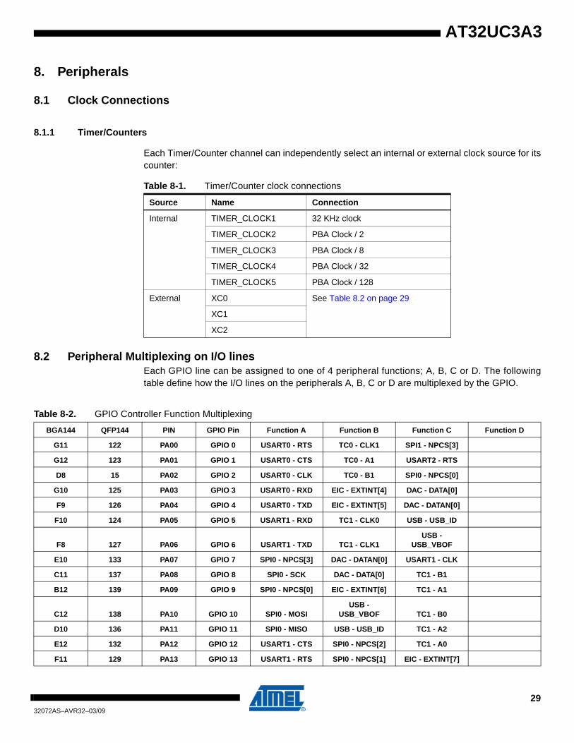
8. Peripherals
8.1 Clock Connections
8.1.1 Timer/Counters
Each Timer/Counter channel can independently select an internal or external clock source for itscounter:
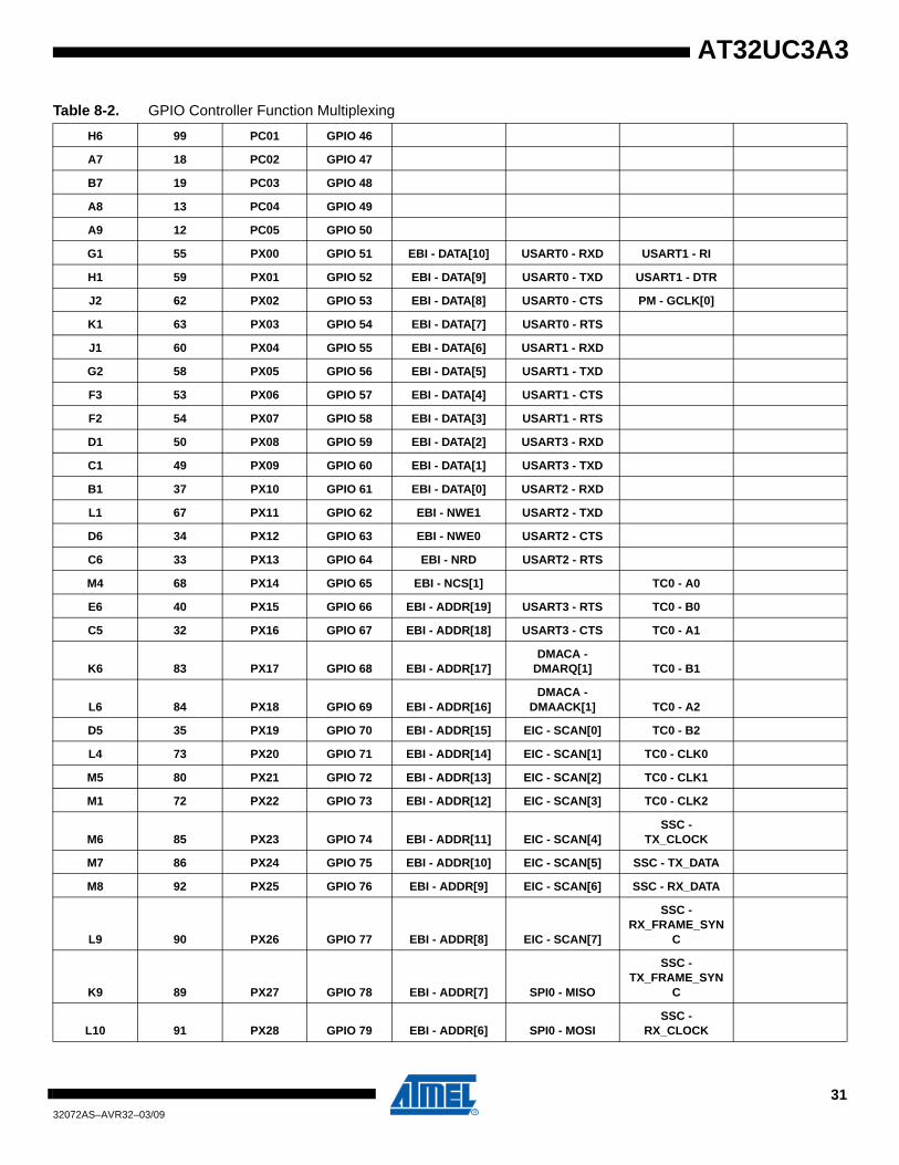
8.2 Peripheral Multiplexing on I/O linesEach GPIO line can be assigned to one of 4 peripheral functions; A, B, C or D. The followingtable define how the I/O lines on the peripherals A, B, C or D are multiplexed by the GPIO.
Table 8-1. Timer/Counter clock connections
Source Name Connection
Internal TIMER_CLOCK1 32 KHz clock
TIMER_CLOCK2 PBA Clock / 2
TIMER_CLOCK3 PBA Clock / 8
TIMER_CLOCK4 PBA Clock / 32
TIMER_CLOCK5 PBA Clock / 128
External XC0 See Table 8.2 on page 29
XC1
XC2
Table 8-2. GPIO Controller Function Multiplexing
BGA144 QFP144 PIN GPIO Pin Function A Function B Function C Function D
8.4.1 Power Manager• Controls integrated oscillators and PLLs• Generates clocks and resets for digital logic• Supports 2 crystal oscillators 4MHZ-16MHz• Supports 2 PLLs 48-150MHz• Supports 32KHz ultra-low power oscillator• Integrated low-power RC oscillator• On-the fly frequency change of CPU, HSB, PBA, and PBB clocks• Sleep modes allow simple disabling of logic clocks, PLLs, and oscillators• Module-level clock gating through maskable peripheral clocks• Wake-up from internal or external interrupts• Generic clocks with wide frequency range provided• Automatic identification of reset sources• Controls brownout detector (BOD), RC oscillator, and bandgap voltage reference through control
and calibration registers
8.4.2 Real Time Counter• 32-bit real-time counter with 16-bit prescaler• Clocked from RC oscillator or 32KHz oscillator• Long delays
– Max timeout 272years• High resolution: Max count frequency 16KHz• Extremely low power consumption• Available in all sleep modes except Static• Interrupt on wrap
8.4.3 Watchdog Timer• Watchdog timer counter with 32-bit prescaler• Clocked from the system RC oscillator (RCSYS)
8.4.4 Interrupt Controller• Autovectored low latency interrupt service with programmable priority
– 4 priority levels for regular, maskable interrupts– One Non-Maskable Interrupt
3532072AS–AVR32–03/09
AT32UC3A3
• Up to 64 groups of interrupts with up to 32 interrupt requests in each
8.4.5 External Interrupts Controller• Dedicated interrupt request for each interrupt• Individually maskable interrupts• Interrupt on rising or falling edge• Interrupt on high or low level• Asynchronous interrupts for sleep modes without clock• Filtering of interrupt lines• Maskable NMI interrupt• Keypad scan support•
8.4.6 Flash Controller• Controls flash block with dual read ports allowing staggered reads.• Supports 0 and 1 wait state bus access.• Allows interleaved burst reads for systems with one wait state, outputting one 32-bit word per
clock cycle.• 32-bit HSB interface for reads from flash array and writes to page buffer.• 32-bit PB interface for issuing commands to and configuration of the controller.• 16 lock bits, each protecting a region consisting of (total number of pages in the flash block / 16)
pages.• Regions can be individually protected or unprotected.• Additional protection of the Boot Loader pages.• Supports reads and writes of general-purpose NVM bits.• Supports reads and writes of additional NVM pages.• Supports device protection through a security bit.• Dedicated command for chip-erase, first erasing all on-chip volatile memories before erasing
flash and clearing security bit.• Interface to Power Manager for power-down of flash-blocks in sleep mode.
8.4.7 HSB Bus Matrix• User Interface on peripheral bus• Configurable Number of Masters (Up to sixteen)• Configurable Number of Slaves (Up to sixteen)• One Decoder for Each Master• Three Different Memory Mappings for Each Master (Internal and External boot, Remap)• One Remap Function for Each Master• Programmable Arbitration for Each Slave
– Round-Robin– Fixed Priority
• Programmable Default Master for Each Slave– No Default Master– Last Accessed Default Master– Fixed Default Master
3632072AS–AVR32–03/09
AT32UC3A3
• One Cycle Latency for the First Access of a Burst• Zero Cycle Latency for Default Master• One Special Function Register for Each Slave (Not dedicated)
8.4.8 External Bus Interface• Optimized for application memory space support• Integrates three external memory controllers:
• Additional logic for NAND Flash/SmartMediaTM and CompactFlashTM support– NAND Flash support: 8-bit as well as 16-bit devices are supported– CompactFlash support: all modes (Attribute Memory, Common Memory, I/O, True IDE) are
supported but the signals _IOIS16 (I/O and True IDE modes) and _ATA SEL (True IDE mode) are not handled.
• Optimized external bus:16-bit data bus– Up to 24-bit Address Bus, Up to 8-Mbytes Addressable– Optimized pin multiplexing to reduce latencies on external memories
• Up to 6 Chip Selects, Configurable Assignment:– Static Memory Controller on Chip Select 0– SDRAM Controller or Static Memory Controller on Chip Select 1– Static Memory Controller on Chip Select 2, Optional NAND Flash support– Static Memory Controller on Chip Select 3, Optional NAND Flash support– Static Memory Controller on Chip Select 4, Optional CompactFlashTM support– Static Memory Controller on Chip Select 5, Optional CompactFlashTM support
8.4.9 Static Memory Controller• 6 chip selects available• 64-Mbytes address space per chip select• 8- or 16-bit data bus• Word, halfword, byte transfers• Byte write or byte select lines• Programmable setup, pulse and hold time for read signals per chip select• Programmable setup, pulse and hold time for write signals per chip select• Programmable data float time per chip select• Compliant with LCD module• External wait request• Automatic switch to slow clock mode• Asynchronous read in page mode supported: page size ranges from 4 to 32 bytes
– 2K, 4K, 8K row address memory parts – SDRAM with two or four internal banks– SDRAM with 16-bit data path
• Programming facilities– Word, halfword, byte access– Automatic page break when memory boundary has been reached– Multibank ping-pong access
3732072AS–AVR32–03/09
AT32UC3A3
– Timing parameters specified by software– Automatic refresh operation, refresh rate is programmable– Automatic update of DS, TCR and PASR parameters (mobile SDRAM devices)
• Energy-saving capabilities– Self-refresh, power-down, and deep power-down modes supported– Supports mobile SDRAM devices
• Error detection– Refresh error interrupt
• SDRAM power-up initialization by software• CAS latency of one, two, and three supported• Auto Precharge command not used
8.4.11 Peripheral DMA Controller• 8 channels• Generates transfers to/from peripherals such as USART, SSC and SPI• Two address pointers/counters per channel allowing double buffering• Performance monitors to measure average and maximum transfer latency
– 9 Hardware Handshaking Interfaces• Memory/Non-Memory Peripherals to Memory/Non-Memory Peripherals Transfer• Single-block DMA Transfer• Multi-block DMA Transfer
– Linked Lists– Auto-Reloading– Contiguous Blocks
• DMA Controller is Always the Flow Controller• Additional Features
– Scatter and Gather Operations– Channel Locking
– Bus Locking– FIFO Mode– Pseudo Fly-by Operation
8.4.13 General-Purpose Input/Output ControllerEach I/O line of the GPIO features:
• Configurable pin-change, rising-edge or falling-edge interrupt on any I/O line• A glitch filter providing rejection of pulses shorter than one clock cycle• Input visibility and output control• Multiplexing of up to four peripheral functions per I/O line• Programmable internal pull-up resistor
Serial Peripheral Interface
• Compatible with an embedded 32-bit microcontroller • Supports communication with serial external devices
– Four chip selects with external decoder support allow communication with up to 15 peripherals
3832072AS–AVR32–03/09
AT32UC3A3
– Serial memories, such as DataFlash and 3-wire EEPROMs– Serial peripherals, such as ADCs, DACs, LCD controllers, CAN controllers and Sensors– External co-processors
• Master or Slave Serial Peripheral Bus Interface– 4 - to 16-bit programmable data length per chip select– Programmable phase and polarity per chip select– Programmable transfer delays between consecutive transfers and between clock and data
per chip select– Programmable delay between consecutive transfers– Selectable mode fault detection
• Connection to Peripheral DMA Controller channel capabilities optimizes data transfers– One channel for the receiver, one channel for the transmitter– Next buffer support– Four character FIFO in reception
8.4.14 Two-Wire Slave Interface• Compatible with I²C standard
– 100 and 400 kbit/s transfer speeds– 7 and 10-bit and General Call addressing
• Compatible with SMBus standard– Hardware Packet Error Checking (CRC) generation and verification with ACK response– SMBALERT interface– 25 ms clock low timeout delay– 25 ms slave cumulative clock low extend time
• Compatible with PMBus• DMA interface for reducing CPU load• Arbitrary transfer lengths, including 0 data bytes• Optional clock stretching if transmit or receive buffers not ready for data transfer• 32-bit Peripheral Bus interface for configuration of the interface
8.4.15 Two-Wire Master Interface• Compatible with I²C standard
– Multi-master support– 100 and 400 kbit/s transfer speeds– 7- and 10-bit and General Call addressing
• Compatible with SMBus standard– Hardware Packet Error Checking (CRC) generation and verification with ACK control– SMBus ALERT interface– 25 ms clock low timeout delay– 10 ms master cumulative clock low extend time– 25 ms slave cumulative clock low extend time
3932072AS–AVR32–03/09
AT32UC3A3
• Compatible with PMBus• Compatible with Atmel Two-Wire Interface Serial Memories• DMA interface for reducing CPU load• Arbitrary transfer lengths, including 0 data bytes• Optional clock stretching if transmit or receive buffers not ready for data transfer
8.4.16 Synchronous Serial Controller• Provides serial synchronous communication links used in audio and telecom applications• Independent receiver and transmitter, common clock divider• Interfaced with two Peripheral DMA Controller channels to reduce processor overhead• Configurable frame sync and data length• Receiver and transmitter can be configured to start automatically or on detection of different
events on the frame sync signal• Receiver and transmitter include a data signal, a clock signa,l and a frame synchronization signal
8.4.17 Universal Synchronous Asynchronous Receiver Transmitter• Programmable Baud Rate Generator• 5- to 9-bit Full-duplex Synchronous or Asynchronous Serial Communications
– 1, 1.5 or 2 Stop Bits in Asynchronous Mode or 1 or 2 Stop Bits in Synchronous Mode– Parity Generation and Error Detection– Framing Error Detection, Overrun Error Detection– MSB- or LSB-first– Optional Break Generation and Detection– By 8 or by 16 Over-sampling Receiver Frequency– Optional Hardware Handshaking RTS-CTS– Optional Modem Signal Management DTR-DSR-DCD-RI– Receiver Time-out and Transmitter Timeguard– Optional Multidrop Mode with Address Generation and Detection
• RS485 with Driver Control Signal• ISO7816, T = 0 or T = 1 Protocols for Interfacing with Smart Cards
– NACK Handling, Error Counter with Repetition and Iteration Limit• IrDA Modulation and Demodulation
– Communication at up to 115.2 Kbps• SPI Mode
– Master or Slave– Serial Clock Programmable Phase and Polarity– SPI Serial Clock (CLK) Frequency up to Internal Clock Frequency CLK_USART/4
• LIN Mode– Compliant with LIN 1.3 and LIN 2.0 specifications– Master or Slave– Processing of frames with up to 256 data bytes– Response Data length can be configurable or defined automatically by the Identifier– Self synchronization in Slave node configuration– Automatic processing and verification of the “Synch Break” and the “Synch Field”– The “Synch Break” is detected even if it is partially superimposed with a data byte– Automatic Identifier parity calculation/sending and verification– Parity sending and verification can be disabled– Automatic Checksum calculation/sending and verification– Checksum sending and verification can be disabled– Support both “Classic” and “Enhanced” checksum types
4032072AS–AVR32–03/09
AT32UC3A3
– Full LIN error checking and reporting– Frame Slot Mode: the Master allocates slots to the scheduled frames automatically.– Generation of the Wakeup signal
• Test Modes– Remote Loopback, Local Loopback, Automatic Echo
• Supports Connection of Two Peripheral DMA Controller Channels (PDCA)– Offers Buffer Transfer without Processor Intervention
8.4.18 USB On-The-Go Interface• Compatible with the USB 2.0 specification• Supports High (480Mbps), Full (12Mbps) and Low (1.5Mbps) speed communication and On-The-
Go• nine pipes/endpoints• 2368 of Embedded Dual-Port RAM (DPRAM) for Pipes/Endpoints• Up to 2 memory banks per Pipe/Endpoint (Not for Control Pipe/Endpoint)• Flexible Pipe/Endpoint configuration and management with dedicated DMA channels• On-Chip UTMI transceiver including Pull-Ups/Pull-downs• On-Chip OTG pad including VBUS analog comparator
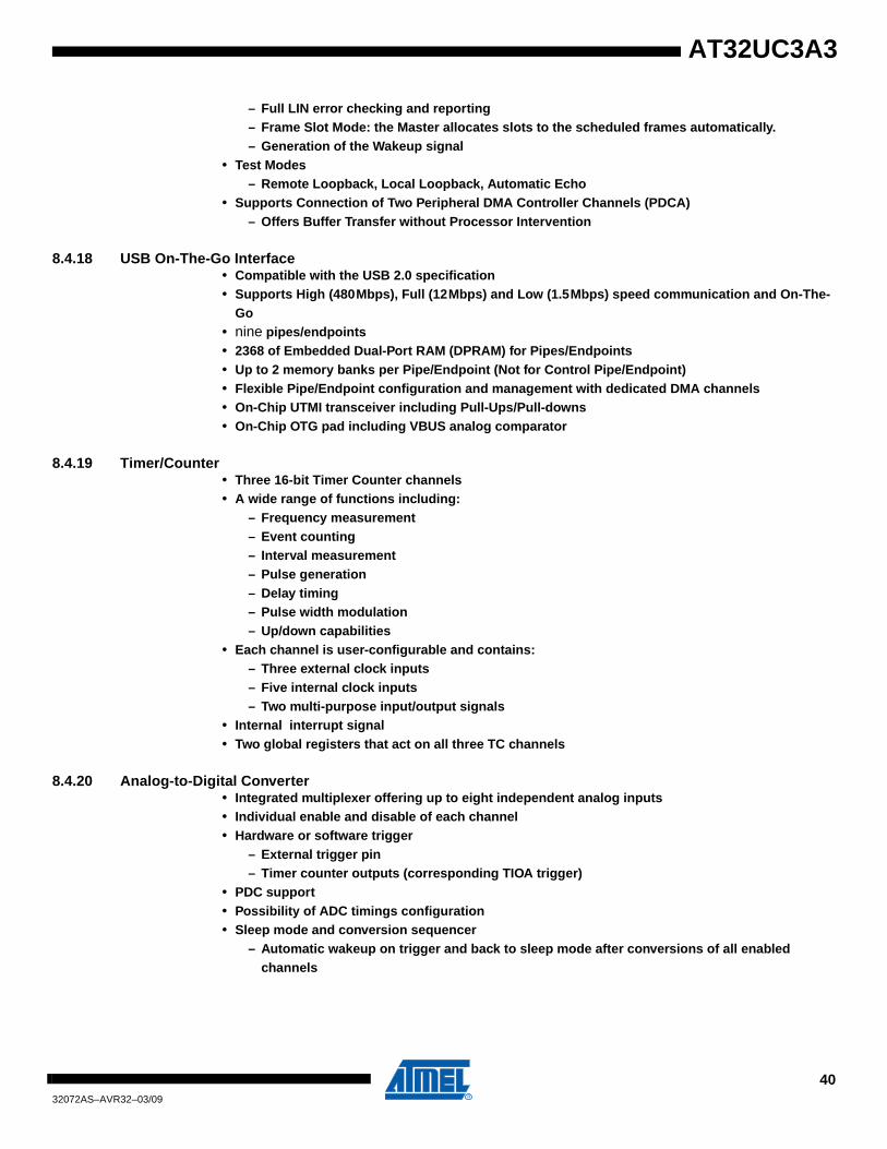
8.4.19 Timer/Counter• Three 16-bit Timer Counter channels• A wide range of functions including:
• Each channel is user-configurable and contains:– Three external clock inputs– Five internal clock inputs– Two multi-purpose input/output signals
• Internal interrupt signal• Two global registers that act on all three TC channels
8.4.20 Analog-to-Digital Converter• Integrated multiplexer offering up to eight independent analog inputs• Individual enable and disable of each channel• Hardware or software trigger
• PDC support• Possibility of ADC timings configuration• Sleep mode and conversion sequencer
– Automatic wakeup on trigger and back to sleep mode after conversions of all enabled channels
4132072AS–AVR32–03/09
AT32UC3A3
8.4.21 HSB Bus Performance Monitor• Allows performance monitoring of High Speed Bus master interfaces
– Up to 4 masters can be monitored– Peripheral Bus access to monitor registers
• The following is monitored– Data transfer cycles– Bus stall cycles– Maximum access latency for a single transfer
• Automatic handling of event overflow
8.4.22 Multimedia Card Interface• Compatible with Multimedia Card specification version 4.2• Compatible with SD Memory Card specification version 2.0• Compatible with SDIO specification version 1.1• Compatible with CE-ATA specification 1.1• Cards clock rate up to master clock divided by two• High Speed mode support• Embedded power management to slow down clock rate when not used• Supports 2 Slots
– Each slot for either a MultiMediaCard bus (up to 30 cards) or an SD Memory Card• Support for stream, block and multi-block data read and write• Supports connection to DMA Controller
– Minimizes processor intervention for large buffer transfers• Built in FIFO (from 16 to 256 bytes) with large memory aperture supporting incremental access• Support for CE-ATA completion cignal disable command• Protection against unexpected modification on-the-Fly of the configuration registers
8.4.23 Error Corrected Code Controller• Hardware Error Corrected Code Generation with two methods :
– Hamming code detection and correction by software (ECC-H)– Reed-Solomon code detection by hardware, correction by hardware or software (ECC-RS)
• Supports NAND Flash and SmartMedia™ devices with 8- or 16-bit data path for ECC-H, and with 8-bit data path for ECC-RS
• Supports NAND Flash and SmartMedia™ with page sizes of 528, 1056, 2112, and 4224 bytes (specified by software)
• ECC_H supports :– One bit correction per page of 512,1024,2048, or 4096 bytes– One bit correction per sector of 512 bytes of data for a page size of 512, 1024, 2048, or 4096
bytes– One bit correction per sector of 256 bytes of data for a page size of 512, 1024, 2048, or 4096
bytes• ECC_RS supports :
– 4 errors correction per sector of 512 bytes of data for a page size of 512, 1024, 2048, and 4096 bytes with 8-bit data path
4232072AS–AVR32–03/09
AT32UC3A3
8.4.24 Advanced Encryption Standart• Compliant with FIPS Publication 197, Advanced Encryption Standard (AES)• 128-bit/192-bit/256-bit cryptographic key• 12/14/16 clock cycles encryption/decryption processing time with a 128-bit/192-bit/256-bit
cryptographic key• Support of the five standard modes of operation specified in the NIST Special Publication 800-
38A, Recommendation for Block Cipher Modes of Operation - Methods and Techniques:– Electronic Code Book (ECB)– Cipher Block Chaining (CBC)– Cipher Feedback (CFB)– Output Feedback (OFB)– Counter (CTR)
• 8-, 16-, 32-, 64- and 128-bit data size possible in CFB mode• Last output data mode allows optimized Message Authentication Code (MAC) generation• Hardware counter measures against differential power analysis attacks• Connection to DMA Controller capabilities optimizes data transfers for all operating modes
– Oversampling ratio fixed 128x– FIR equalization filter– Digital interpolation filter: Comb4– 3rd Order Sigma-Delta D/A converters
• Digital bitstream outputs• Parallel interface• Connected to DMA Controller for background transfer without CPU intervention
8.4.26 On-Chip Debug• Debug interface in compliance with IEEE-ISTO 5001-2003 (Nexus 2.0) Class 2+• JTAG access to all on-chip debug functions• Advanced program, data, ownership, and watchpoint trace supported• NanoTrace JTAG-based trace access• Auxiliary port for high-speed trace information• Hardware support for 6 program and 2 data breakpoints• Unlimited number of software breakpoints supported• Automatic CRC check of memory regions
8.4.27 JTAG and Boundary Scan• IEEE1149.1 compliant JTAG Interface• Boundary-Scan Chain for board-level testing• Direct memory access and programming capabilities through JTAG interface• On-Chip Debug access in compliance with IEEE-ISTO 5001-2003 (Nexus 2.0)•
4332072AS–AVR32–03/09
AT32UC3A3
9. Boot SequenceThis chapter summarizes the boot sequence of the AT32UC3A3. The behavior after power-up iscontrolled by the Power Manager. For specific details, refer to Section 8. ”Power Manager (PM)”on page 36.
9.1 Starting of ClocksAfter power-up, the device will be held in a reset state by the Power-On Reset circuitry, until thepower has stabilized throughout the device. Once the power has stabilized, the device will usethe internal RC Oscillator as clock source.
On system start-up, the PLLs are disabled. All clocks to all modules are running. No clocks havea divided frequency, all parts of the system receives a clock with the same frequency as theinternal RC Oscillator.
9.2 Fetching of Initial InstructionsAfter reset has been released, the AVR32 UC CPU starts fetching instructions from the resetaddress, which is 0x8000_0000. This address points to the first address in the internal Flash.
The code read from the internal Flash is free to configure the system to use for example thePLLs, to divide the frequency of the clock routed to some of the peripherals, and to gate theclocks to unused peripherals.
4432072AS–AVR32–03/09
AT32UC3A3
10. Electrical Characteristics
10.1 Absolute Maximum Ratings*
10.2 DC Characteristics
Operating Temperature.................................... -40°C to +85°C *NOTICE: Stresses beyond those listed under “Absolute Maximum Ratings” may cause permanent dam-age to the device. This is a stress rating only and functional operation of the device at these or other conditions beyond those indicated in the operational sections of this specification is not implied. Exposure to absolute maximum rating conditions for extended periods may affect device reliability.
Storage Temperature .......................................................... ....-60°C to +150°C
Voltage on Input Pin with respect to Ground ........................................-0.3V to 3.6V
Maximum Operating Voltage (VDDCORE) ..................... 1.95V
Maximum Operating Voltage (VDDIO).............................. 3.6V
Total DC Output Current on all I/O Pinfor TQFP144 packag ................................................... 370 mAfor TBGA144 package ................................................. 370 mA
The following characteristics are applicable to the operating temperature range: TA = -40°C to 85°C, unless otherwise spec-ified and are certified for a junction temperature up to TJ = 100°C.
Symbol Parameter Condition Min. Typ. Max. Units
VVDDIO DC Supply Peripheral I/Os 3.0 3.6 V
VIL Input Low-level Voltage -0.3 +0.8 V
VIH Input High-level Voltage 2.0VVDDIO+0
.3V
VOL Output Low-level VoltageIOL=-2mA for Pin drive x1IOL=-4mA for Pin drive x2
IOL=-8mA for Pin drive x3
0.4V
VOH Output High-level Voltage
IOL=2mA for Pin drive x1
IOL=4mA for Pin drive x2
IOL=8mA for Pin drive x3
VVDDIO-0.4V
ILEAK Input Leakage Current Pullup resistors disabled µA
CIN Input Capacitance 7 pF
RPULLUP Pull-up Resistance 9 15 25 Ohm
IO
Output Current
Pin drive x1Pin drive x2
Pin drive x3
See Table 10-1
2.04.0
8.0
mA
ISC Static Current
On VVDDIN = 3.3V,
CPU in static modeTA =25°C TBD µA
TA =85°C TBD µA
4532072AS–AVR32–03/09
AT32UC3A3
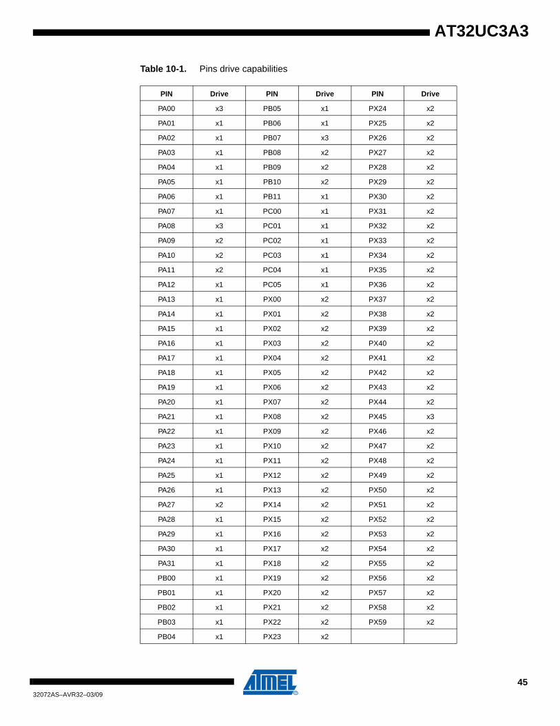
Table 10-1. Pins drive capabilities
PIN Drive PIN Drive PIN Drive
PA00 x3 PB05 x1 PX24 x2
PA01 x1 PB06 x1 PX25 x2
PA02 x1 PB07 x3 PX26 x2
PA03 x1 PB08 x2 PX27 x2
PA04 x1 PB09 x2 PX28 x2
PA05 x1 PB10 x2 PX29 x2
PA06 x1 PB11 x1 PX30 x2
PA07 x1 PC00 x1 PX31 x2
PA08 x3 PC01 x1 PX32 x2
PA09 x2 PC02 x1 PX33 x2
PA10 x2 PC03 x1 PX34 x2
PA11 x2 PC04 x1 PX35 x2
PA12 x1 PC05 x1 PX36 x2
PA13 x1 PX00 x2 PX37 x2
PA14 x1 PX01 x2 PX38 x2
PA15 x1 PX02 x2 PX39 x2
PA16 x1 PX03 x2 PX40 x2
PA17 x1 PX04 x2 PX41 x2
PA18 x1 PX05 x2 PX42 x2
PA19 x1 PX06 x2 PX43 x2
PA20 x1 PX07 x2 PX44 x2
PA21 x1 PX08 x2 PX45 x3
PA22 x1 PX09 x2 PX46 x2
PA23 x1 PX10 x2 PX47 x2
PA24 x1 PX11 x2 PX48 x2
PA25 x1 PX12 x2 PX49 x2
PA26 x1 PX13 x2 PX50 x2
PA27 x2 PX14 x2 PX51 x2
PA28 x1 PX15 x2 PX52 x2
PA29 x1 PX16 x2 PX53 x2
PA30 x1 PX17 x2 PX54 x2
PA31 x1 PX18 x2 PX55 x2
PB00 x1 PX19 x2 PX56 x2
PB01 x1 PX20 x2 PX57 x2
PB02 x1 PX21 x2 PX58 x2
PB03 x1 PX22 x2 PX59 x2
PB04 x1 PX23 x2
4632072AS–AVR32–03/09
AT32UC3A3
10.3 Regulator characteristics
10.3.1 Electrical characteristics
10.3.2 Decoupling requirements
10.3.3 BOD
Table 10-2. BODLEVEL Values
The values in Table 10-2 describes the values of the BODLEVEL in the flash FGPFRL register.
10.4 Power Consumption The values in Table 10-3 and Table 10-4 on page 48 are measured values of power consump-tion with operating conditions as follows:
•VDDIO = 3.3V
•TA = 25°C, TA = 85°C
•I/Os are configured in input, pull-up enabled.
Symbol Parameter Condition Min. Typ. Max. Units
VVDDIN Supply voltage (input) 2.7 3.3 3.6 V
VVDDCORE Supply voltage (output) 1.81 1.85 1.89 V
IOUT
Maximum DC output current with VVDDIN = 3.3V 100 mA
Maximum DC output current with VVDDIN = 2.7V 90 mA
Symbol Parameter Condition Typ. Techno. Units
CIN1 Input Regulator Capacitor 1 1 NPO nF
CIN2 Input Regulator Capacitor 2 4.7 X7R uF
COUT1 Output Regulator Capacitor 1 470 NPO pF
COUT2 Output Regulator Capacitor 2 2.2 X7R uF
BODLEVEL Value Typ. Units.
111111b 1.58 V
101000b 1.62 V
100000b 1.67 V
011000b 1.77 V
000000b 1.92 V
4732072AS–AVR32–03/09
AT32UC3A3
Figure 10-1. Measurement setup
InternalVoltage
Regulator
Amp0
VDDANA
VDDIO
VDDIN
VDDCORE
GNDPLL
Amp1
GNDCORE
4832072AS–AVR32–03/09
AT32UC3A3
These figures represent the power consumption measured on the power supplies.
10.5 Clock CharacteristicsThese parameters are given in the following conditions:
• VDDCORE = 1.8V
Table 10-3. Power Consumption for Different Modes(1)
Mode ConditionsConsumption
Typ. Unit
Active
CPU running from flash.CPU clocked from PLL0 at f MHz
Voltage regulator is on.
XIN0 : external clock. (1)
XIN1 stopped. XIN32 stopped
PLL0 running
All peripheral clocks activated.GPIOs on internal pull-up.
JTAG unconnected with ext pull-up.
f = 12 MHz 10 mA
f = 24 MHz 18 mA
f = 36MHz 27 mA
f = 50 MHz 34 mA
f = 60 MHz 42 mA
Static
Typ : Ta = 25 °C
CPU is in static mode
GPIOs on internal pull-up.All peripheral clocks de-activated.
DM and DP pins connected to ground.
XIN0,Xin1 and XIN2 are stopped
on Amp0 0 uA
on Amp1 <100 uA
1. Core frequency is generated from XIN0 using the PLL so that 140 MHz < fpll0 < 160 MHz and 10 MHz < fxin0 < 12MHz
Table 10-4. Power Consumption by Peripheral in Active Mode
Peripheral Consumption Unit
GPIO 37
µA/MHz
SMC 10
SDRAMC 4
ADC 18
EBI 31
INTC 25
TWI 14
PDCA 30
RTC 7
SPI 13
SSC 13
TC 10
USART 35
4932072AS–AVR32–03/09
AT32UC3A3
• Ambient Temperature = 25°C
10.5.1 CPU/HSB Clock Characteristics
10.5.2 PBA Clock Characteristics
10.5.3 PBB Clock Characteristics
10.5.4 XIN Clock Characteristics
Note: 1. These characteristics apply only when the Main Oscillator is in bypass mode (i.e., when MOSCEN = 0 and OSCBYPASS = 1 in the CKGR_MOR register.)
10.6 Crystal Oscillator CharacteristisThe following characteristics are applicable to the operating temperature range: TA = -40°C to 85°C and worst case ofpower supply, unless otherwise specified.
Table 10-5. Core Clock Waveform Parameters
Symbol Parameter Conditions Min Max Units
1/(tCPCPU) CPU Clock Frequency 66 MHz
tCPCPU CPU Clock Period 15.5 ns
Table 10-6. PBA Clock Waveform Parameters
Symbol Parameter Conditions Min Max Units
1/(tCPPBA) PBA Clock Frequency 66 MHz
tCPPBA PBA Clock Period 15.5 ns
Table 10-7. PBB Clock Waveform Parameters
Symbol Parameter Conditions Min Max Units
1/(tCPPBB) PBB Clock Frequency 66 MHz
tCPPBB PBB Clock Period 15.5 ns
Table 10-8. XIN Clock Electrical Characteristics
Symbol Parameter Conditions Min Max Units
1/(tCPXIN) XIN Clock Frequency 3 24 MHz
tCPXIN XIN Clock Period 20.0 ns
tCHXIN XIN Clock High Half-period 0.4 x tCPXIN 0.6 x tCPXIN
tCLXIN XIN Clock Low Half-period 0.4 x tCPXIN 0.6 x tCPXIN
CIN XIN Input Capacitance (1) TBD pF
RIN XIN Pulldown Resistor (1) TBD kΩ
5032072AS–AVR32–03/09
AT32UC3A3
10.6.1 32 KHz Oscillator Characteristics
Note: 1. RS is the equivalent series resistance, CL is the equivalent load capacitance.
10.6.2 Main Oscillators Characteristics
Notes: 1. CS is the shunt capacitance
10.6.3 PLL Characteristics
Note: 1. Startup time depends on PLL RC filter. A calculation tool is provided by Atmel.
Table 10-9. 32 KHz Oscillator Characteristics
Symbol Parameter Conditions Min Typ Max Unit
1/(tCP32KHz) Crystal Oscillator Frequency 32 768 Hz
CL Equivalent Load Capacitance 6 12.5 pF
Duty Cycle TBD TBD %
tST Startup Time RS = TBD kΩ, CL = TBD pF(1) TBD ms
Table 10-10. Main Oscillator Characteristics
Symbol Parameter Conditions Min Typ Max Unit
1/(tCPMAIN) Crystal Oscillator Frequency 3 16 MHz
CL1, CL2Internal Load Capacitance
(CL1 = CL2)12 pF
CL Equivalent Load Capacitance TBD pF
Duty Cycle 40 50 60 %
tST Startup Time TBD ms
IOSC Current ConsumptionActive mode @TBD MHz TBD µA
Standby mode @TBD V TBD µA
Table 10-11. Phase Lock Loop Characteristics
Symbol Parameter Conditions Min Typ Max Unit
FOUT Output Frequency 80 240 MHz
FIN Input Frequency TBD TBD MHz
IPLL Current Consumptionactive mode TBD mA
standby mode TBD µA
5132072AS–AVR32–03/09
AT32UC3A3
10.7 ADC Characteristics
Notes: 1. Corresponds to 13 clock cycles at 5 MHz: 3 clock cycles for track and hold acquisition time and 10 clock cycles for conversion.
2. Corresponds to 15 clock cycles at 8 MHz: 5 clock cycles for track and hold acquisition time and 10 clock cycles for conversion.
Table 10-12. Channel Conversion Time and ADC Clock
Parameter Conditions Min Typ Max Units
ADC Clock Frequency 10-bit resolution mode 5 MHz
ADC Clock Frequency 8-bit resolution mode 8 MHz
Startup Time Return from Idle Mode 20 µs
Track and Hold Acquisition Time 600 ns
Conversion Time ADC Clock = 5 MHz 2 µs
Conversion Time ADC Clock = 8 MHz 1.25 µs
Throughput Rate ADC Clock = 5 MHz 384(1) kSPS
Throughput Rate ADC Clock = 8 MHz 533(2) kSPS
Table 10-13. Analog Inputs
Parameter Min Typ Max Units
Input Voltage Range 0 VDDANA
Input Leakage Current TBD µA
Input Capacitance 17 pF
Table 10-14. Transfer Characteristics
Parameter Conditions Min Typ Max Units
Resolution 10 Bit
Absolute Accuracy f=5MHz 0.8 LSB
Integral Non-linearity f=5MHz 0.35 0.5 LSB
Differential Non-linearity f=5MHz 0.3 0.5 LSB
Offset Error f=5MHz -0.5 0.5 LSB
Gain Error f=5MHz -0.5 0.5 LSB
5232072AS–AVR32–03/09
AT32UC3A3
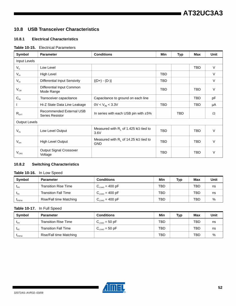
10.8 USB Transceiver Characteristics
10.8.1 Electrical Characteristics
10.8.2 Switching Characteristics
Table 10-15. Electrical Parameters
Symbol Parameter Conditions Min Typ Max Unit
Input Levels
VIL Low Level TBD V
VIH High Level TBD V
VDI Differential Input Sensivity |(D+) - (D-)| TBD V
VCM
Differential Input Common Mode Range
TBD TBD V
CIN Transceiver capacitance Capacitance to ground on each line TBD pF
I Hi-Z State Data Line Leakage 0V < VIN < 3.3V TBD TBD µA
REXT
Recommended External USB Series Resistor
In series with each USB pin with ±5% TBD Ω
Output Levels
VOL Low Level OutputMeasured with RL of 1.425 kΩ tied to 3.6V
TBD TBD V
VOH High Level OutputMeasured with RL of 14.25 kΩ tied to GND
SPI10 MOSI Setup time before SPCK falls (slave) 3.3V domain (1) 0 ns
SPI11 MOSI Hold time after SPCK falls (slave) 3.3V domain (1) 1 ns
Table 10-27. Ethernet MAC Signals
Symbol Parameter Conditions Min (ns) Max (ns)
EMAC1 Setup for EMDIO from EMDC rising Load: 20pF(2)
EMAC2 Hold for EMDIO from EMDC rising Load: 20pF(2)
EMAC3 EMDIO toggling from EMDC falling Load: 20pF(2)
Table 10-28. Ethernet MAC MII Specific Signals
Symbol Parameter Conditions Min (ns) Max (ns)
EMAC4 Setup for ECOL from ETXCK rising Load: 20pF (1) 3
EMAC5 Hold for ECOL from ETXCK rising Load: 20pF (1) 0
EMAC6 Setup for ECRS from ETXCK rising Load: 20pF (1) 3
EMAC7 Hold for ECRS from ETXCK rising Load: 20pF (1) 0
EMAC8 ETXER toggling from ETXCK rising Load: 20pF (1) 15
EMAC9 ETXEN toggling from ETXCK rising Load: 20pF (1) 15
EMAC10 ETX toggling from ETXCK rising Load: 20pF (1) 15
EMAC11 Setup for ERX from ERXCK Load: 20pF (1) 1
6332072AS–AVR32–03/09
AT32UC3A3
Note: 1. VVDDIO from 3.0V to 3.6V, maximum external capacitor = 20 pF
Figure 10-10. Ethernet MAC MII Mode
EMAC12 Hold for ERX from ERXCK Load: 20pF (1) 1.5
EMAC13 Setup for ERXER from ERXCK Load: 20pF (1) 1
EMAC14 Hold for ERXER from ERXCK Load: 20pF (1) 0.5
EMAC15 Setup for ERXDV from ERXCK Load: 20pF (1) 1.5
EMAC16 Hold for ERXDV from ERXCK Load: 20pF (1) 1
Table 10-28. Ethernet MAC MII Specific Signals
Symbol Parameter Conditions Min (ns) Max (ns)
EMDC
EMDIO
ECOL
ECRS
ETXCK
ETXER
ETXEN
ETX[3:0]
ERXCK
ERX[3:0]
ERXER
ERXDV
EMAC3EMAC1 EMAC2
EMAC4 EMAC5
EMAC6 EMAC7
EMAC8
EMAC9
EMAC10
EMAC11 EMAC12
EMAC13 EMAC14
EMAC15 EMAC16
6432072AS–AVR32–03/09
AT32UC3A3
Figure 10-11. Ethernet MAC RMII Mode
10.13 Flash Characteristics
The following table gives the device maximum operating frequency depending on the field FWSof the Flash FSR register. This field defines the number of wait states required to access theFlash Memory.
Table 10-29. Ethernet MAC RMII Specific Signals
Symbol Parameter Min (ns) Max (ns)
EMAC21 ETXEN toggling from EREFCK rising 7 14.5
EMAC22 ETX toggling from EREFCK rising 7 14.7
EMAC23 Setup for ERX from EREFCK 1.5
EMAC24 Hold for ERX from EREFCK 0
EMAC25 Setup for ERXER from EREFCK 1.5
EMAC26 Hold for ERXER from EREFCK 0
EMAC27 Setup for ECRSDV from EREFCK 1.5
EMAC28 Hold for ECRSDV from EREFCK 0
EREFCK
ETXEN
ETX[1:0]
ERX[1:0]
ERXER
ECRSDV
EMAC21
EMAC22
EMAC23 EMAC24
EMAC25 EMAC26
EMAC27 EMAC28
Table 10-30. Flash Wait States
FWS Read Operations Maximum Operating Frequency (MHz)
0 1 cycle 36
1 2 cycles 66
6532072AS–AVR32–03/09
AT32UC3A3
11. Mechanical Characteristics
11.1 Thermal Considerations
11.1.1 Thermal DataTable 11-1 summarizes the thermal resistance data depending on the package.
11.1.2 Junction TemperatureThe average chip-junction temperature, TJ, in °C can be obtained from the following:
1.
2.
where:
• θJA = package thermal resistance, Junction-to-ambient (°C/W), provided in Table 11-1 on page 65.
• θJC = package thermal resistance, Junction-to-case thermal resistance (°C/W), provided in Table 11-1 on page 65.
• θHEAT SINK = cooling device thermal resistance (°C/W), provided in the device datasheet.
• PD = device power consumption (W) estimated from data provided in the section ”Regulator characteristics” on page 46.
• TA = ambient temperature (°C).
From the first equation, the user can derive the estimated lifetime of the chip and decide if acooling device is necessary or not. If a cooling device is to be fitted on the chip, the secondequation should be used to compute the resulting average chip-junction temperature TJ in °C.
Table 11-1. Thermal Resistance Data
Symbol Parameter Condition Package Typ Unit
θJA Junction-to-ambient thermal resistance Still Air TQFP144 TBD°C/W
AT32UC3A3256S AT32UC3A3256S-ALUT 144 lead LQFP Tray Industrial (-40⋅C to 85⋅C)
AT32UC3A3256S-ALUR 144 lead LQFP Reels Industrial (-40⋅C to 85⋅C)
AT32UC3A3256S-CTUT 144 balls TBGA Tray Industrial (-40⋅C to 85⋅C)
AT32UC3A3256S-CTUR 144 balls TBGA Reels Industrial (-40⋅C to 85⋅C)
AT32UC3A3256 AT32UC3A3256-ALUT 144 lead LQFP Tray Industrial (-40⋅C to 85⋅C)
AT32UC3A3256-ALUR 144 lead LQFP Reels Industrial (-40⋅C to 85⋅C)
AT32UC3A3256-CTUT 144 balls TBGA Tray Industrial (-40⋅C to 85⋅C)
AT32UC3A3256-CTUR 144 balls TBGA Reels Industrial (-40⋅C to 85⋅C)
AT32UC3A3128S AT32UC3A3128S-ALUT 144 lead LQFP Tray Industrial (-40⋅C to 85⋅C)
AT32UC3A3128S-ALUR 144 lead LQFP Reels Industrial (-40⋅C to 85⋅C)
AT32UC3A3128S-CTUT 144 balls TBGA Tray Industrial (-40⋅C to 85⋅C)
AT32UC3A3128S-CTUR 144 balls TBGA Reels Industrial (-40⋅C to 85⋅C)
AT32UC3A3128 AT32UC3A3128-ALUT 144 lead LQFP Tray Industrial (-40⋅C to 85⋅C)
AT32UC3A3128-ALUR 144 lead LQFP Reels Industrial (-40⋅C to 85⋅C)
AT32UC3A3128-CTUT 144 balls TBGA Tray Industrial (-40⋅C to 85⋅C)
AT32UC3A3128-CTUR 144 balls TBGA Reels Industrial (-40⋅C to 85⋅C)
AT32UC3A364S AT32UC3A364S-ALUT 144 lead LQFP Tray Industrial (-40⋅C to 85⋅C)
AT32UC3A364S-ALUR 144 lead LQFP Reels Industrial (-40⋅C to 85⋅C)
AT32UC3A364S-CTUT 144 balls TBGA Tray Industrial (-40⋅C to 85⋅C)
AT32UC3A364S-CTUR 144 balls TBGA Reels Industrial (-40⋅C to 85⋅C)
AT32UC3A364 AT32UC3A364-ALUT 144 lead LQFP Tray Industrial (-40⋅C to 85⋅C)
AT32UC3A364-ALUR 144 lead LQFP Reels Industrial (-40⋅C to 85⋅C)
AT32UC3A364-CTUT 144 balls TBGA Tray Industrial (-40⋅C to 85⋅C)
AT32UC3A364-CTUR 144 balls TBGA Reels Industrial (-40⋅C to 85⋅C)
7032072AS–AVR32–03/09
AT32UC3A3
13. Errata
13.1 Rev. E
13.1.1 Processor and Architecture
1. LDM instruction with PC in the register list and without ++ increments RpFor LDM with PC in the register list: the instruction behaves as if the ++ field is always set, iethe pointer is always updated. This happens even if the ++ field is cleared. Specifically, theincrement of the pointer is done in parallel with the testing of R12.Fix/WorkaroundNone.
13.1.2 ADC
1. Sleep Mode activation needs additional A to D conversionIf the ADC sleep mode is activated when the ADC is idle the ADC will not enter sleep modebefore after the next AD conversion.
Fix/WorkaroundActivate the sleep mode in the mode register and then perform an AD conversion.
13.1.3 SPI
1. SPI Bad Serial Clock Generation on 2nd chip_select when SCBR = 1, CPOL=1 andNCPHA=0When multiple CS are in use, if one of the baudrate equals to 1 and one of the others doesn'tequal to 1, and CPOL=1 and CPHA=0, then an additional pulse will be generated on SCK.Fix/workaroundWhen multiple CS are in use, if one of the baudrate equals 1, the other mustalso equal 1 if CPOL=1 and CPHA=0.
2. SPI Disable does not work in Slave modeFix/workaroundRead the last received data then perform a Software reset.
13.2 Rev. D
13.2.1 Processor and Architecture
1. LDM instruction with PC in the register list and without ++ increments RpFor LDM with PC in the register list: the instruction behaves as if the ++ field is always set, iethe pointer is always updated. This happens even if the ++ field is cleared. Specifically, theincrement of the pointer is done in parallel with the testing of R12.Fix/WorkaroundNone.
2. RETE instruction does not clear SREG[L] from interrupts.The RETE instruction clears SREG[L] as expected from exceptions.Fix/Workaround
7132072AS–AVR32–03/09
AT32UC3A3
When using the STCOND instruction, clear SREG[L] in the stacked value of SR beforereturning from interrupts with RETE.
3. Exceptions when system stack is protected by MPURETS behaves incorrectly when MPU is enabled and MPU is configured so thatsystem stack is not readable in unprivileged mode.Fix/WorkaroundWorkaround 1: Make system stack readable in unprivileged mode, or Workaround 2: Return from supervisor mode using rete instead of rets. This requires :1. Changing the mode bits from 001b to 110b before issuing the instruction.Updating the mode bits to the desired value must be done using a single mtsr instruction soit is done atomically. Even if this step is described in general as not safe in the UC technicalreference guide, it is safe in this very specific case.2. Execute the RETE instruction.
4. Multiply instructions do not work on RevD.All the multiply instructions do not work.Fix/WorkaroundDo not use the multiply instructions.
13.2.2 ADC
1. Sleep Mode activation needs additional A to D conversionIf the ADC sleep mode is activated when the ADC is idle the ADC will not enter sleep modebefore after the next AD conversion.
Fix/WorkaroundActivate the sleep mode in the mode register and then perform an AD conversion.
13.2.3 SPI
1. SPI Bad Serial Clock Generation on 2nd chip_select when SCBR = 1, CPOL=1 andNCPHA=0When multiple CS are in use, if one of the baudrate equals to 1 and one of the others doesn'tequal to 1, and CPOL=1 and CPHA=0, then an additional pulse will be generated on SCK.Fix/workaroundWhen multiple CS are in use, if one of the baudrate equals 1, the other mustalso equal 1 if CPOL=1 and CPHA=0.
2. SPI Disable does not work in Slave modeFix/workaroundRead the last received data then perform a Software reset.
13.2.4 TWI
1. TWIM Version Register is zeroTWIM Version Register (VR) is zero instead of 0x100.Fix/WorkaroundNone.
7232072AS–AVR32–03/09
AT32UC3A3
14. Datasheet Revision HistoryPlease note that the referring page numbers in this section are referred to this document. Thereferring revision in this section are referring to the document revision.
14.1 Rev. A – 03/09
1. Initial revision.
i32072AS–AVR32–03/09
AT32UC3A3
Table of Contents
Features ..................................................................................................... 1
Disclaimer: The information in this document is provided in connection with Atmel products. No license, express or implied, by estoppel or otherwise, to anyintellectual property right is granted by this document or in connection with the sale of Atmel products. EXCEPT AS SET FORTH IN ATMEL’S TERMS AND CONDI-TIONS OF SALE LOCATED ON ATMEL’S WEB SITE, ATMEL ASSUMES NO LIABILITY WHATSOEVER AND DISCLAIMS ANY EXPRESS, IMPLIED OR STATUTORYWARRANTY RELATING TO ITS PRODUCTS INCLUDING, BUT NOT LIMITED TO, THE IMPLIED WARRANTY OF MERCHANTABILITY, FITNESS FOR A PARTICULARPURPOSE, OR NON-INFRINGEMENT. IN NO EVENT SHALL ATMEL BE LIABLE FOR ANY DIRECT, INDIRECT, CONSEQUENTIAL, PUNITIVE, SPECIAL OR INCIDEN-TAL DAMAGES (INCLUDING, WITHOUT LIMITATION, DAMAGES FOR LOSS OF PROFITS, BUSINESS INTERRUPTION, OR LOSS OF INFORMATION) ARISING OUTOF THE USE OR INABILITY TO USE THIS DOCUMENT, EVEN IF ATMEL HAS BEEN ADVISED OF THE POSSIBILITY OF SUCH DAMAGES. Atmel makes norepresentations or warranties with respect to the accuracy or completeness of the contents of this document and reserves the right to make changes to specificationsand product descriptions at any time without notice. Atmel does not make any commitment to update the information contained herein. Unless specifically providedotherwise, Atmel products are not suitable for, and shall not be used in, automotive applications. Atmel’s products are not intended, authorized, or warranted for useas components in applications intended to support or sustain life.