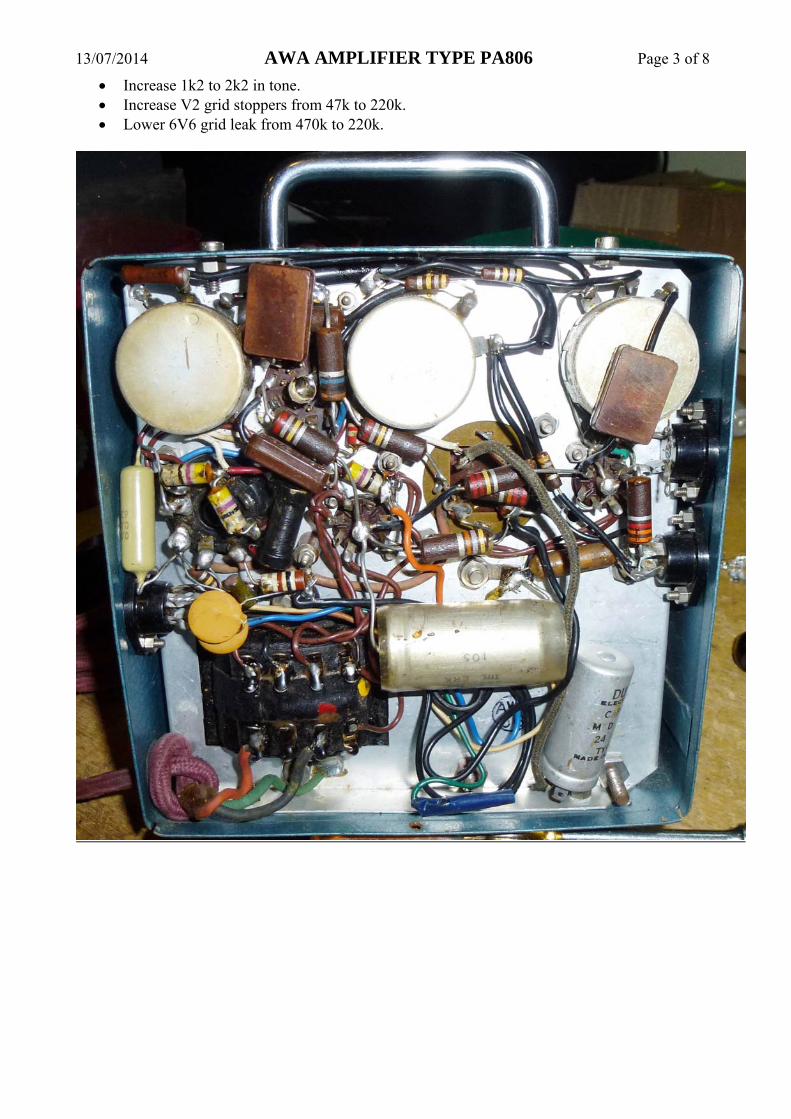
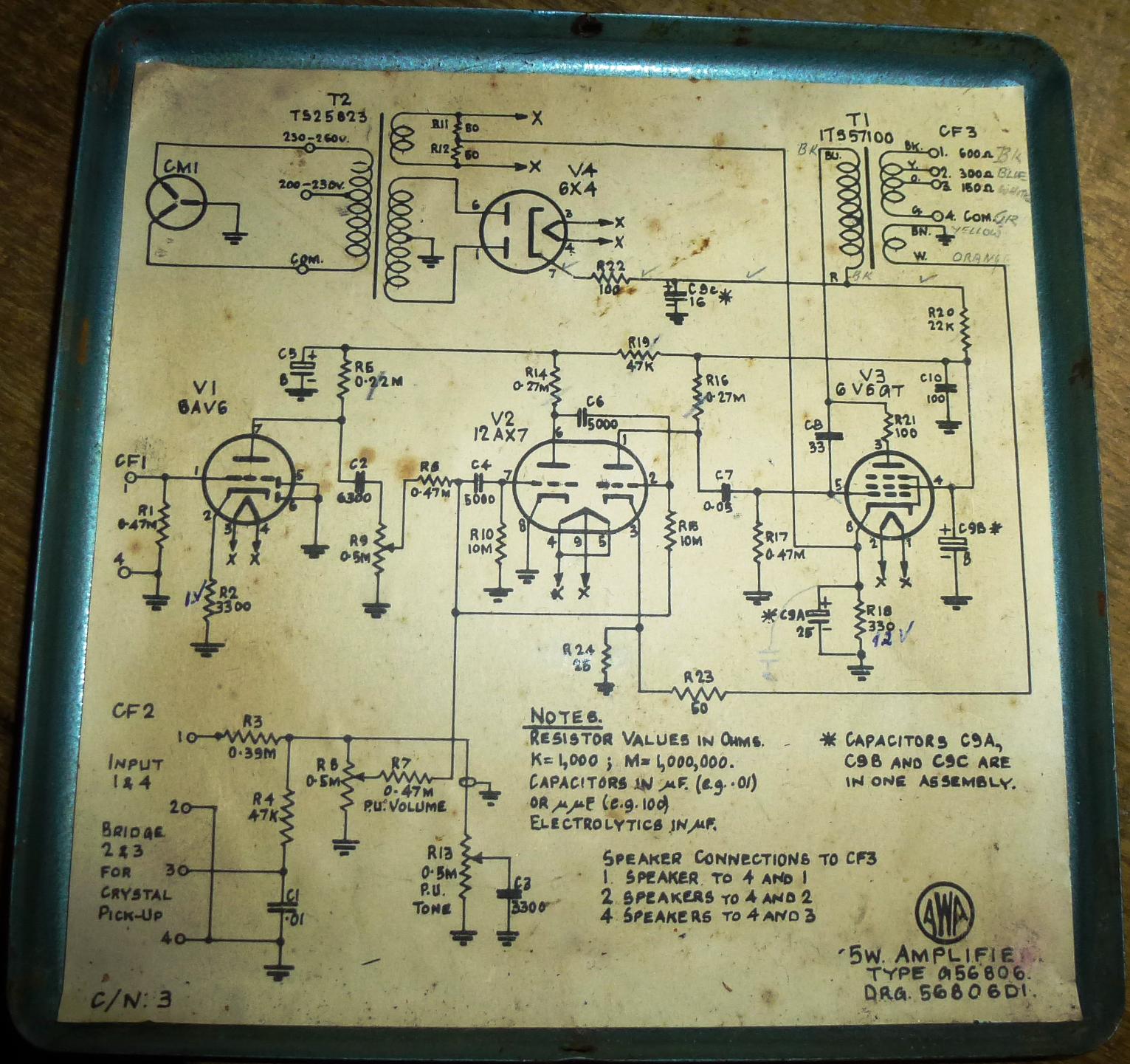
13/07/2014 AWA AMPLIFIER TYPE PA806 Page 1 of 8 1. Summary AWA 5 Watt Amplifier Model PA806, S.N. 359. eBay Jun 2013 Type G56806. DRG 56806D1 C/N.3 1.1 Original design One microphone and one P.U. input channel PA amplifier. 6AV6 unbypassed cathode triode stage for MIC channel with MIV Vol pot loading. PU input into PU Tone and PU Vol pots then both inputs summed to 12AX7 grid-leak biased stage, and then to another grid-leak biased 12AX7 with separate OT winding feedback to cathode, and then to 6V6GT SE output stage with bypassed cathode bias and RC filtered screen. 6X4 full wave rectifier with added series resistance to capacitor input B+. RC filtering to screen and driver, and RC filter to preamps. Heater humdinger to 6V6 cathode elevation. Power transformer TS25823; 0,220-230,230-260V; 350-0-350V; 6.3V 2A. Output Transformer 1TS57100; 5W, 8.8k ; 0-50Ω-150Ω-600Ω; 0-0.1Ω. Valves 6AV6 Radiotron F? 24 12AX7 Radiotron 3A6/573 6V6GT Radiotron 21 NH T3 6X4 Radiotron GH 6 Capacitors UCC type ERK 105. UCC wax Ducon can EC3C 18. Ducon ECT106 47 Pots IRC B7 59774T63 Condition: Very good case. PT mounting bolt loose (lug with cathode connection loose). One knob rear holder partly broken & two felts missing. OT wires possibly changed (colours and pencilled markings and tape) and added cathode bypass cap for 6V6 and changed C7 and C8. 6V6 with asbestos (?) mat top and depressed front panel to fit tube in. Connector pin inserts splayed. One triode in 12AX7 poor with grid leak. Chassis marked AWA 56. Part types and possible part dates indicate late 1950’s build.
Transcript
13/07/2014 AWA AMPLIFIER TYPE PA806 Page 1 of 8
1. Summary AWA 5 Watt Amplifier Model PA806, S.N. 359. eBay Jun 2013 Type G56806. DRG 56806D1 C/N.3
1.1 Original design One microphone and one P.U. input channel PA amplifier. 6AV6 unbypassed cathode triode stage for MIC channel with MIV Vol pot loading. PU input into PU Tone and PU Vol pots then both inputs summed to 12AX7 grid-leak biased stage, and then to another grid-leak biased 12AX7 with separate OT winding feedback to cathode, and then to 6V6GT SE output stage with bypassed cathode bias and RC filtered screen. 6X4 full wave rectifier with added series resistance to capacitor input B+. RC filtering to screen and driver, and RC filter to preamps. Heater humdinger to 6V6 cathode elevation. Power transformer TS25823; 0,220-230,230-260V; 350-0-350V; 6.3V 2A. Output Transformer 1TS57100; 5W, 8.8k ; 0-50Ω-150Ω-600Ω; 0-0.1Ω. Valves 6AV6 Radiotron F? 24
Ducon can EC3C 18. Ducon ECT106 47 Pots IRC B7 59774T63 Condition: Very good case. PT mounting bolt loose (lug with cathode connection loose). One knob rear holder partly broken & two felts missing. OT wires possibly changed (colours and pencilled markings and tape) and added cathode bypass cap for 6V6 and changed C7 and C8. 6V6 with asbestos (?) mat top and depressed front panel to fit tube in. Connector pin inserts splayed. One triode in 12AX7 poor with grid leak. Chassis marked AWA 56. Part types and possible part dates indicate late 1950’s build.
13/07/2014 AWA AMPLIFIER TYPE PA806 Page 2 of 8
Design Issues:
Mains earthed using PT mounting bolt (which was loose). No mains fuse or switch. Messy chassis grounding. Volume pots before gain stages (except MIC input) Grid leak biasing. OT impedances (measured secondaries different from schematic).
1.2 Modifications
MIC input socket (pins 1, 4) remain as input 6AV6 with added 22k grid stopper and 4.7uF cathode bypass. Reduced V2B grid stopper from V1 to 47k, and take V2B to V2A with 47k grid stopper.
Removed feedback. Shunt impedance tone control across V2B output – LC series notch at 1kHz on one end of
pot – LC parallel bandpass on other end of pot (using same L) – shunt 27kΩ to even out attenuation for mid-tone position. 780Ω now 1k2; 4n7 now 10nF.
PU pot across V2A. 6V6 with added 10k grid stopper and 680Ω screen stopper. Mains fuse and switch. MOV across primary. Replaced electrolytics and wax paper caps. PT secondary half-HT winding damaged during restoration. B+ now derived from full-
bridge off half-HT winding using 1N4007s plus 6X4 diodes in positive half of bridge (series ss diodes with 6X4).
Added 2.3H and 15uF LC filter to VS1. 660V MOV across OT primary. Speaker output (16Ω) on pins 1,4.
To do:
13/07/2014 AWA AMPLIFIER TYPE PA806 Page 3 of 8
Increase 1k2 to 2k2 in tone. Increase V2 grid stoppers from 47k to 220k. Lower 6V6 grid leak from 470k to 220k.
13/07/2014 AWA AMPLIFIER TYPE PA806 Page 4 of 8
13/07/2014 AWA AMPLIFIER TYPE PA806 Page 5 of 8
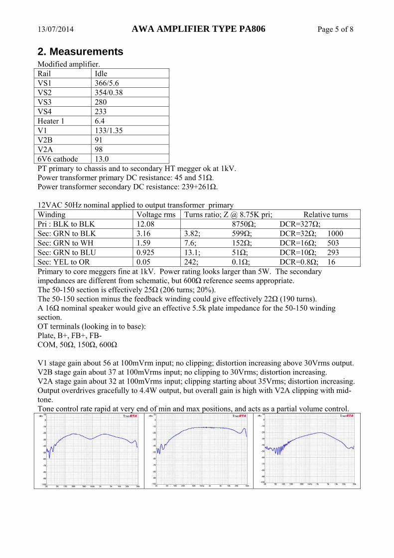
2. Measurements Modified amplifier. Rail Idle VS1 366/5.6 VS2 354/0.38 VS3 280 VS4 233 Heater 1 6.4 V1 133/1.35 V2B 91 V2A 98 6V6 cathode 13.0 PT primary to chassis and to secondary HT megger ok at 1kV. Power transformer primary DC resistance: 45 and 51Ω. Power transformer secondary DC resistance: 239+261Ω. 12VAC 50Hz nominal applied to output transformer primary Winding Voltage rms Turns ratio; Z @ 8.75K pri; Relative turns Pri : BLK to BLK 12.08 8750Ω; DCR=327Ω; Sec: GRN to BLK 3.16 3.82; 599Ω; DCR=32Ω; 1000 Sec: GRN to WH 1.59 7.6; 152Ω; DCR=16Ω; 503 Sec: GRN to BLU 0.925 13.1; 51Ω; DCR=10Ω; 293 Sec: YEL to OR 0.05 242; 0.1Ω; DCR=0.8Ω; 16 Primary to core meggers fine at 1kV. Power rating looks larger than 5W. The secondary impedances are different from schematic, but 600Ω reference seems appropriate. The 50-150 section is effectively 25Ω (206 turns; 20%). The 50-150 section minus the feedback winding could give effectively 22Ω (190 turns). A 16Ω nominal speaker would give an effective 5.5k plate impedance for the 50-150 winding section. OT terminals (looking in to base): Plate, B+, FB+, FB- COM, 50Ω, 150Ω, 600Ω V1 stage gain about 56 at 100mVrm input; no clipping; distortion increasing above 30Vrms output. V2B stage gain about 37 at 100mVrms input; no clipping to 30Vrms; distortion increasing. V2A stage gain about 32 at 100mVrms input; clipping starting about 35Vrms; distortion increasing. Output overdrives gracefully to 4.4W output, but overall gain is high with V2A clipping with mid-tone. Tone control rate rapid at very end of min and max positions, and acts as a partial volume control.
3.2 Driver stages – 12AX7 For the 1st half 12AX7, V2B: VS3 = 233V; Va=91V; Ia=0.52mA; RLdc=270k; 10M grid leak. For the 2nd half 12AX7, V2A: VS2 = 280V; Va=98V; Ia=0.67mA; RLdc=270k; 10M grid leak.
3.3 Output Stage Class A single-ended 6V6GT output stage with 330R cathode bias and 25uF bypass and an 8.8KΩ plate impedance OT, but effective plate impedance is lower at 5.5k for a nominal 16Ω speaker. The output valve bias current target is nominally 70% of the maximum recommended plate dissipation of 14W for the 6V6GT: Ibias(max) = 0.7 * Pd / Vb = 0.7 * 14 / (350-10V) = 29mA, which gives 9.5V bias (0.3W) for 330Ω. But with 344V VS2, the cathode voltage is 13.3V, and hence cathode current is 40mA, of which anode current is about 35mA. The output valve plate-cathode sits below VS2 by about 13V across cathode, and (330+100)x0.035 = 15V for OT primary DCR and anode stopper. With VS2=344V, then Vak = 316V. Anode dissipation is about (344-13-15)*0.035 = 11W (80% of design max). Screen voltage supply VS3 is about 4mA*15k= 60V lower than VS2. Screen voltage sits at about 344-58-13= 273V. VS3 sags at high signal levels to about 244V, with average screen current increasing from about 4mA to about 6mA, and screen dropper could drop up to an additional 14V, so screen voltage could dip to about 244-14-13 = 217V when anode current peaks. Low OT reflected impedance will limit available voltage swing at cut-off. Idle cathode current was raised by increasing VS3 screen voltage (22k dropper lowered to 15k).
12AX7
13/07/2014 AWA AMPLIFIER TYPE PA806 Page 8 of 8
3.4 Power Supplies The full bridge rectifier circuit uses a 350V secondary HT winding to give 500VDC peak, which exceeds the 450V rating of the filter caps. A 220k 2W loading resistor is added to B+ to alleviate the peak voltage at turn on and if tubes pulled, and to discharge caps if tubes pulled. Only one 6.3VAC secondary is available for heaters. Heater loading is 0.6 + 0.45 + 0.3 + 0.3 = 1.65A. The effective source resistance is comprised of the reflected power transformer primary resistance = 45Ω x (350/240)2 = 95Ω; plus the secondary resistance = 240Ω; which sums to 335Ω. Datasheet effective source resistance should be 150Ω for a secondary supply of 325Vrms, based on 8uF capacitor-input filter and up to 70mA load. 6V6 cathode loading is about 40mA. C9B and C5 are increased from 8uF to 15uF/450V. Inductor (Wurlitzer 500407, 2.3H @ 50mA) and 15uF added after VS1 to lower hum from 5V to 0.2Vrms on VS2, and lower 6V6 idle voltage a bit.