ASIX ELECTRONICS CORPORATION Released Date: 12/13/2011 4F, NO.8, Hsin Ann Rd., Hsinchu Science Park, Hsin-Chu City, Taiwan, R.O.C. 300 TEL: 886-3-579-9500 FAX: 886-3-579-9558 http://www.asix.com.tw/ AX88772A/AX88172A Low-pin-count USB 2.0 to 10/100M Fast Ethernet Controller Features Single chip USB 2.0 to 10/100M Fast Ethernet controller – AX88772A Single chip USB 2.0 to MII, single chip MII to Ethernet and USB Bridging controller in Dual-PHY mode (US Patent Pending) – AX88172A USB Device Interface Integrates on-chip USB 2.0 transceiver and SIE compliant to USB Spec 1.1 and 2.0 Supports USB Full and High Speed modes with Bus-Power or Self-Power capability Supports 4 or 6 programmable endpoints on USB interface High performance packet transfer rate over USB bus using proprietary burst transfer mechanism (US Patent Approval) Supports USB to Ethernet bridging or vice versa in hardware Fast Ethernet Controller Integrates 10/100Mbps Fast Ethernet MAC/PHY IEEE 802.3 10BASE-T/100BASE-TX compatible Supports twisted pair crossover detection and auto-correction (HP Auto-MDIX) Embedded 16KB SRAM for RX packet buffering and 8KB SRAM for TX packet buffering Supports both Full-duplex with flow control and Half-duplex with backpressure operation Supports 2 VLAN ID filtering, received VLAN Tag (4 bytes) can be stripped off or preserved MAC/PHY loop-back diagnostic capability Support Wake-on-LAN Function Supports Suspend Mode and Remote Wakeup via Link-up, Magic packet, MS wakeup frame and external pin Optional PHY power down during Suspend Mode Versatile External Media Interface Optional MII interface in MAC mode allows AX88172A to work with external 100BASE-FX Ethernet PHY or HomePNA PHY Optional Reverse-MII or Reverse-RMII interface in PHY mode allows AX88172A to work with external HomePlug PHY or glueless MAC-to-MAC connections Optional Reverse-MII interface in Dual-PHY mode allows AX88172A to act as an Ethernet PHY or USB 2.0 PHY for external MAC device that needs Ethernet and USB in system application Supports 256/512 bytes (93c56/93c66) of serial EEPROM (for storing USB Descriptors) Supports automatic loading of Ethernet ID, USB Descriptors and Adapter Configuration from EEPROM after power-on initialization Provides optional serial interface, I2C, SPI and UART Integrates on-chip voltage regulator and only requires a single 3.3V power supply 12MHz and 25Mhz clock input from either crystal or oscillator source Integrates on-chip power-on reset circuit Small form factor with 64-pin LQFP (AX88772A) or 80-pin TQFP (AX88172A) RoHS compliant package Operating temperature range: 0°C to 70°C. *IEEE is a registered trademark of the Institute of Electrical and Electronic Engineers, Inc. *All other trademarks and registered trademark are the property of their respective holders. Product Description The AX88772A/AX88172A Low-pin-count USB 2.0 to 10/100M Fast Ethernet controller is a high performance and highly integrated ASIC which enables low cost, small form factor, and simple plug-and-play Fast Ethernet network connection capability for desktops, notebook PC’s, Ultra-Mobile PC’s, docking stations, game consoles, digital-home appliances, and any embedded system using a standard USB port. The AX88772A/AX88172A features a USB interface to communicate with a USB Host Controller and is compliant with USB specification V1.1 and V2.0. The AX88772A/AX88172A implements 10/100Mbps Ethernet LAN function based on IEEE802.3, and IEEE802.3u standards with 24KB of embedded SRAM for packet buffering. The AX88772A/AX88172A integrates an on-chip 10/100Mbps Ethernet PHY to simplify system design. The AX88172A provides an optional External Media Interface (EMI) for external PHY or external MAC for different application purposes. The EMI can be a media-independent interface (MII) for implementing 100BASE-FX Ethernet or HomePNA functions. The EMI can also be a Reverse-MII or Reverse Reduced-MII (Reverse-RMII) for glueless MAC-to-MAC connections to any MCU with Ethernet MAC MII or RMII interface. In addition, the EMI can be configured to Dual-PHY mode allowing AX88172A to act as an Ethernet PHY or USB 2.0 PHY for external MAC device that needs Ethernet and USB interfaces in their system applications. The optional serial interface such as I2C, SPI, and UART are provided as a control channel from the USB Host Controller to communicate with the external MCU chip. Document No: AX88x72A/V1.08/12/13/11
Transcript
ASIX ELECTRONICS CORPORATION Released Date: 12/13/2011 4F, NO.8, Hsin Ann Rd., Hsinchu Science Park, Hsin-Chu City, Taiwan, R.O.C. 300 TEL: 886-3-579-9500 FAX: 886-3-579-9558 http://www.asix.com.tw/
AX88772A/AX88172A Low-pin-count
USB 2.0 to 10/100M Fast Ethernet Controller Features
Single chip USB 2.0 to 10/100M Fast Ethernet controller – AX88772A
Single chip USB 2.0 to MII, single chip MII to Ethernet and USB Bridging controller in Dual-PHY mode (US Patent Pending) – AX88172A
USB Device Interface Integrates on-chip USB 2.0 transceiver and SIE
compliant to USB Spec 1.1 and 2.0 Supports USB Full and High Speed modes with
Bus-Power or Self-Power capability Supports 4 or 6 programmable endpoints on USB
interface High performance packet transfer rate over USB bus
using proprietary burst transfer mechanism (US Patent Approval)
Supports USB to Ethernet bridging or vice versa in hardware
Fast Ethernet Controller Integrates 10/100Mbps Fast Ethernet MAC/PHY IEEE 802.3 10BASE-T/100BASE-TX compatible Supports twisted pair crossover detection and
auto-correction (HP Auto-MDIX) Embedded 16KB SRAM for RX packet buffering and
8KB SRAM for TX packet buffering Supports both Full-duplex with flow control and
Half-duplex with backpressure operation Supports 2 VLAN ID filtering, received VLAN Tag (4
bytes) can be stripped off or preserved MAC/PHY loop-back diagnostic capability
Support Wake-on-LAN Function Supports Suspend Mode and Remote Wakeup via
Link-up, Magic packet, MS wakeup frame and external pin
Optional PHY power down during Suspend Mode
Versatile External Media Interface Optional MII interface in MAC mode allows AX88172A
to work with external 100BASE-FX Ethernet PHY or HomePNA PHY
Optional Reverse-MII or Reverse-RMII interface in PHY mode allows AX88172A to work with external HomePlug PHY or glueless MAC-to-MAC connections
Optional Reverse-MII interface in Dual-PHY mode allows AX88172A to act as an Ethernet PHY or USB 2.0 PHY for external MAC device that needs Ethernet and USB in system application
Supports 256/512 bytes (93c56/93c66) of serial EEPROM (for storing USB Descriptors)
Supports automatic loading of Ethernet ID, USB Descriptors and Adapter Configuration from EEPROM after power-on initialization
Provides optional serial interface, I2C, SPI and UART Integrates on-chip voltage regulator and only requires a single 3.3V power supply 12MHz and 25Mhz clock input from either crystal or oscillator source
Integrates on-chip power-on reset circuit Small form factor with 64-pin LQFP (AX88772A) or 80-pin TQFP (AX88172A) RoHS compliant package
Operating temperature range: 0°C to 70°C. *IEEE is a registered trademark of the Institute of Electrical and
Electronic Engineers, Inc. *All other trademarks and registered trademark are the property of their
respective holders.
Product Description The AX88772A/AX88172A Low-pin-count USB 2.0 to 10/100M Fast Ethernet controller is a high performance and highly integrated ASIC which enables low cost, small form factor, and simple plug-and-play Fast Ethernet network connection capability for desktops, notebook PC’s, Ultra-Mobile PC’s, docking stations, game consoles, digital-home appliances, and any embedded system using a standard USB port. The AX88772A/AX88172A features a USB interface to communicate with a USB Host Controller and is compliant with USB specification V1.1 and V2.0. The AX88772A/AX88172A implements 10/100Mbps Ethernet LAN function based on IEEE802.3, and IEEE802.3u standards with 24KB of embedded SRAM for packet buffering. The AX88772A/AX88172A integrates an on-chip 10/100Mbps Ethernet PHY to simplify system design. The AX88172A provides an optional External Media Interface (EMI) for external PHY or external MAC for different application purposes. The EMI can be a media-independent interface (MII) for implementing 100BASE-FX Ethernet or HomePNA functions. The EMI can also be a Reverse-MII or Reverse Reduced-MII (Reverse-RMII) for glueless MAC-to-MAC connections to any MCU with Ethernet MAC MII or RMII interface. In addition, the EMI can be configured to Dual-PHY mode allowing AX88172A to act as an Ethernet PHY or USB 2.0 PHY for external MAC device that needs Ethernet and USB interfaces in their system applications. The optional serial interface such as I2C, SPI, and UART are provided as a control channel from the USB Host Controller to communicate with the external MCU chip.
2.0 SIGNAL DESCRIPTION ................................................................................................................................... 17
3.0 FUNCTION DESCRIPTION ............................................................................................................................. 24
3.1 USB CORE AND INTERFACE............................................................................................................................... 24 3.2 10/100M ETHERNET PHY ................................................................................................................................. 24 3.3 MAC CORE ....................................................................................................................................................... 24 3.4 OPERATION MODE ............................................................................................................................................. 25 3.5 STATION MANAGEMENT (STA) ......................................................................................................................... 29 3.6 MEMORY ARBITER ............................................................................................................................................ 31 3.7 USB TO ETHERNET BRIDGE ............................................................................................................................... 31 3.8 SERIAL EEPROM LOADER ................................................................................................................................ 31 3.9 GENERAL PURPOSE I/O...................................................................................................................................... 31 3.10 SERIAL INTERFACE CONTROLLER ...................................................................................................................... 31 3.11 CLOCK GENERATION ......................................................................................................................................... 32 3.12 RESET GENERATION .......................................................................................................................................... 34 3.13 VOLTAGE REGULATOR ...................................................................................................................................... 34
4.0 SERIAL EEPROM MEMORY MAP ............................................................................................................... 35
5.0 USB CONFIGURATION STRUCTURE .......................................................................................................... 39
5.1 USB CONFIGURATION ....................................................................................................................................... 39 5.2 USB INTERFACE ................................................................................................................................................ 39 5.3 USB ENDPOINTS ................................................................................................................................................ 39
6.0 USB COMMANDS ............................................................................................................................................. 40
6.1 USB STANDARD COMMANDS ............................................................................................................................ 40 6.2 USB VENDOR COMMANDS ................................................................................................................................ 41
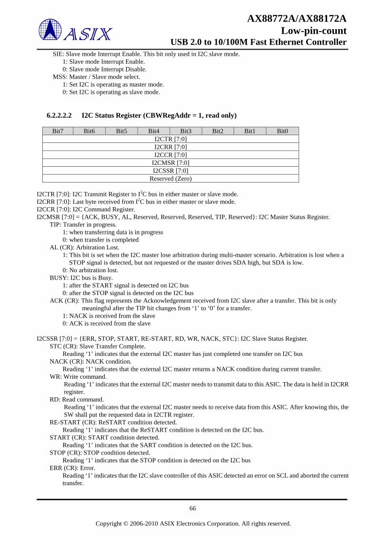
6.2.1 Detailed Register Description ................................................................................................................... 42 6.2.1.1 Rx/Tx SRAM Read Register (02h, read only) .................................................................................. 42 6.2.1.2 Rx/Tx SRAM Write Register (03h, write only) ................................................................................ 42 6.2.1.3 Software Station Management Control Register (06h, write only) ................................................ 43 6.2.1.4 PHY Read Register (07h, read only) ................................................................................................. 43 6.2.1.5 PHY Write Register (08h, write only) ............................................................................................... 43 6.2.1.6 Station Management Status Register (09h, read only) .................................................................... 43 6.2.1.7 Hardware Station Management Control Register (0Ah, write only) ............................................. 44 6.2.1.8 SROM Read Register (0Bh, read only) ............................................................................................. 44 6.2.1.9 SROM Write Register (0Ch, write only) .......................................................................................... 44 6.2.1.10 Write SROM Enable (0Dh, write only) ......................................................................................... 44 6.2.1.11 Write SROM Disable (0Eh, write only) ........................................................................................ 44 6.2.1.12 Rx Control Register (0Fh, read only and 10h, write only) .......................................................... 45 6.2.1.13 IPG/IPG1/IPG2 Control Register (11h, read only and 12h, write only) .................................... 46 6.2.1.14 Node ID Register (13h, read only and 14h, write only) ............................................................... 46 6.2.1.15 Multicast Filter Array (15h, read only and 16h, write only) ....................................................... 47 6.2.1.16 Test Register (17h, write only) ...................................................................................................... 48 6.2.1.17 Ethernet / HomePNA PHY Address Register (19h, read only) ................................................... 48 6.2.1.18 Medium Status Register (1Ah, read only) and Medium Mode Register (1Bh, write only) ...... 49
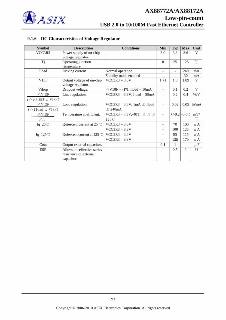
9.1 DC CHARACTERISTICS ....................................................................................................................................... 90 9.1.1 Absolute Maximum Ratings ...................................................................................................................... 90 9.1.2 Recommended Operating Condition ......................................................................................................... 90 9.1.3 Leakage Current and Capacitance ........................................................................................................... 91 9.1.4 DC Characteristics of 3.3V I/O Pins ........................................................................................................ 91 9.1.5 DC Characteristics of 3.3V with 5V Tolerance I/O Pins .......................................................................... 92 9.1.6 DC Characteristics of Voltage Regulator ................................................................................................. 93
9.2 POWER CONSUMPTION ...................................................................................................................................... 94 9.3 POWER-UP SEQUENCE ....................................................................................................................................... 95 9.4 AC TIMING CHARACTERISTICS .......................................................................................................................... 96
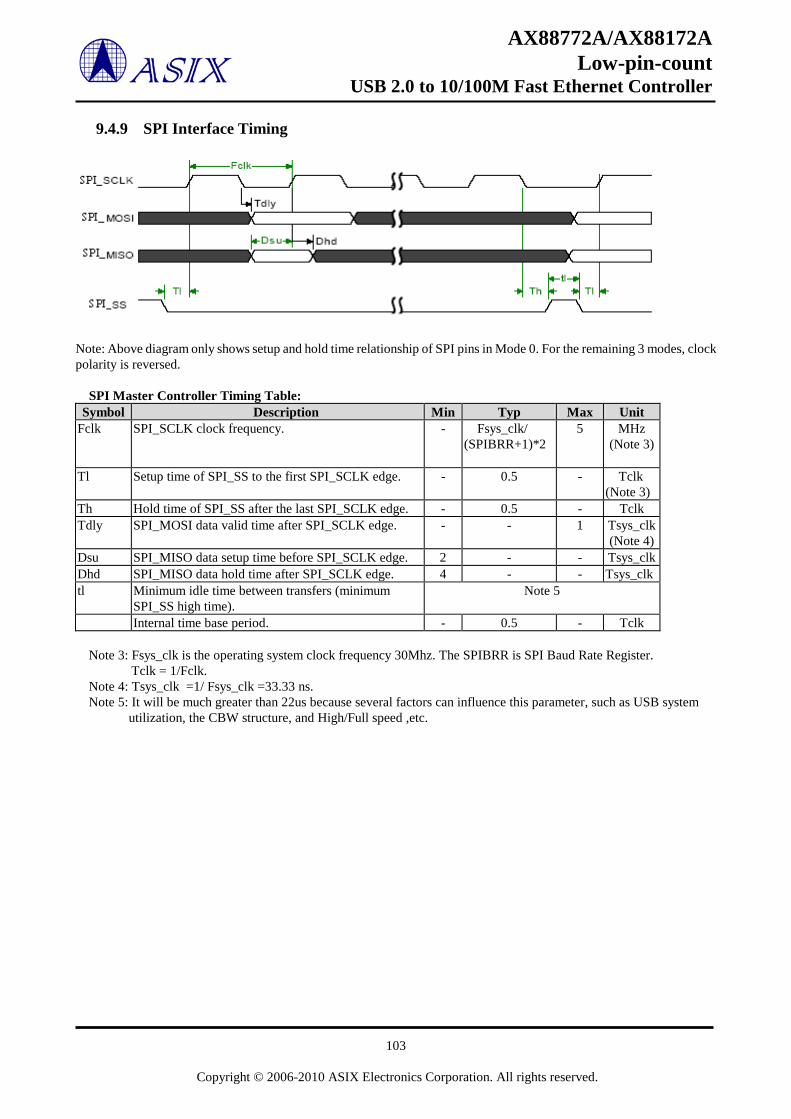
9.4.11 USB Transceiver Interface Timing ......................................................................................................... 106
10.0 PACKAGE INFORMATION .......................................................................................................................... 108
11.0 ORDERING INFORMATION ........................................................................................................................ 110
12.0 REVISION HISTORY ..................................................................................................................................... 111
APPENDIX A. DEFAULT WAKE-ON-LAN (WOL) READY MODE ................................................................... 113
APPENDIX B. ETHERNET PHY POWER AND RESET CONTROL .................................................................. 116
1.0 Introduction 1.1 General Description The AX88772A/AX88172A Low-pin-count USB 2.0 to 10/100M Fast Ethernet controller is a high performance and highly integrated ASIC which enables low cost, small form factor, and simple plug-and-play Fast Ethernet network connection capability for desktops, notebook PC’s, Ultra-Mobile PC’s, docking stations, game consoles, digital-home appliances, and any embedded system using a standard USB port. The AX88772A/AX88172A features a USB interface to communicate with a USB Host Controller and is compliant with USB specification V1.1 and V2.0. The AX88772A/AX88172A implements a 10/100Mbps Ethernet LAN function based on IEEE802.3, and IEEE802.3u standards with 24KB of embedded SRAM for packet buffering. The AX88772A/AX88172A integrates an on-chip 10/100Mbps Ethernet PHY to simplify system design. The AX88172A provides an optional External Media Interface (EMI) for external PHY or external MAC for different application purposes. The EMI can be a media-independent interface (MII) for implementing 100BASE-FX Ethernet or HomePNA functions. The EMI can also be a Reverse-MII or Reverse Reduced-MII (Reverse-RMII) for glueless MAC-to-MAC connections to any MCU with Ethernet MAC MII or RMII interface. In addition, the EMI can be configured to Dual-PHY mode allowing AX88172A to act as an Ethernet PHY or USB 2.0 PHY for external MAC device that needs Ethernet and USB interfaces in their system applications. The optional serial interface such as I2C, SPI, and UART are provided as a control channel from the USB Host Controller to communicate with the external MCU chip. The AX88772A/AX88172A needs 12MHz clock for USB operation and 25Mhz clock for Fast Ethernet operation. The AX88772A is housed in the 64-pin LQFP and the AX88172A is housed in the 80-pin TQFP RoHS compliant package.
1.2 Block Diagram
Figure 7 : AX88772A/AX88172A Block Diagram
DP/DM
RXIP/RXIN TXOP/TXON
GPIO_2~0
MAC Core
Memory Arbiter
USB to Ethernet Bridge
USB Core and Interfaces
STA
SEEPROM Loader I/F
EECS EECK EEDIO
24KB SRAM
General Purpose I/O
10/100M Ethernet
PHY
Serial I/F Controller:
UART/I2C/SPI SI_3~0
AX88172A only External Media Interface MII / Reverse-MII / Reverse-RMII MDC / MDIO
2.0 Signal Description The following abbreviations apply to the following pin description table.
I18 Input, 1.8V AO Analog Output I3 Input, 3.3V AB Analog Bi-directional I/O I5 Input, 3.3V with 5V tolerant PU Internal Pull Up (75K) O3 Output, 3.3V PD Internal Pull Down (75K) O5 Output, 3.3V with 5V tolerant P Power Pin B5 Bi-directional I/O, 3.3V with 5V
tolerant S
T Schmitt Trigger Tri-stateable
AI Analog Input Note: Every output or bi-directional I/O pin is 8mA driving strength.
2.1 AX88772A 64-pin Pinout Description
Table 1 : AX88772A 64-pin Pinout Description Pin Name Type Pin No Pin Description
USB Interface DP AB 57 USB 2.0 data positive pin. DM AB 56 USB 2.0 data negative pin. VBUS I5/PD/S 48 VBUS pin input. Please connect to USB bus power. XTL12P I3 51 12Mhz ±0.005%crystal or oscillator clock input. This clock is needed for
USB PHY transceiver to operate. XTL12N O3 52 12Mhz crystal or oscillator clock output. RREF AI 55 For USB PHY’s internal biasing. Please connect to analog GND through a
resistor (12.1Kohm ±1%). Serial EEPROM Interface
EECK B5/PD/T
35 EEPROM Clock. EECK is an output clock to EEPROM to provide timing reference for the transfer of EECS, and EEDIO signals. EECK only drive high / low when access EEPROM otherwise keep at tri-state and internal pull-down.
EECS B5/PD/T
36 EEPROM Chip Select. EECS is asserted high synchronously with respect to rising edge of EECK as chip select signal. EECS only drive high / low when access EEPROM otherwise keep at tri-state and internal pull-down.
EEDIO B5/PU/T
37 EEPROM Data In. EEDIO is the serial output data to EEPROM’s data input pin and is synchronous with respect to the rising edge of EECK. EEDIO only drive high / low when access EEPROM otherwise keep at tri-state and internal pull-up.
Ethernet PHY Interface XTL25P I18 62 25Mhz ± 0.005% crystal or oscillator clock input. This clock is needed for
the embedded 10/100M Ethernet PHY to operate. XTL25N O18 63 25Mhz crystal or oscillator clock output. RXIP AB 4 Receive data input positive pin for both 10BASE-T and 100BASE-TX. RXIN AB 5 Receive data input negative pin for both 10BASE-T and 100BASE-TX. TXOP AB 7 Transmit data output positive pin for both 10BASE-T and 100 BASE-TX TXON AB 8 Transmit data output negative pin for both 10BASE-T and 100 BASE-TX RSET_BG AO 1 For Ethernet PHY’s internal biasing. Please connect to GND through a
12.1Kohm ±1% resistor. LINK_LED O5 20 Link status LED indicator. This pin drives low continuously when the
Ethernet link is up and drives low and high in turn (blinking) when Ethernet PHY is in receiving or transmitting state.
FDX_LED O5 18 Full Duplex and collision detected LED indicator. This pin drives low when the Ethernet PHY is in full-duplex mode and drives high when in half duplex mode. When in half duplex mode and the Ethernet PHY detects collision, it will be driven low (or blinking).
SPEED_LED O5 19 Ethernet speed LED indicator. This pin drives low when the Ethernet PHY is in 100BASE-TX mode and drives high when in 10BASE-T mode.
Misc. Pins RESET_N I5/PU/S 42 Chip reset input. Active low. This is the external reset source used to reset
this chip. This input feeds to the internal power-on reset circuitry, which provides the main reset source of this chip. After completing reset, EEPROM data will be loaded automatically.
EXTWAKEUP_N I5/PU/S 24 Remote-wakeup trigger from external pin. EXTWAKEUP_N should be asserted low for more than 2 cycles of 12MHz clock to be effective.
GPIO_2 B5/PD 26 General Purpose Input/ Output Pin 2. GPIO_1 B5/PD 27 General Purpose Input/ Output Pin 1. This pin is default as input pin after
power-on reset. This pin is also for Default WOL Ready Mode setting; please refer to section 2.3 Settings.
GPIO_0/PME B5/PD 28 General Purpose Input/ Output Pin 0 or PME (Power Management Event). This pin is default as input pin after power-on reset. GPIO_0 also can be defined as PME output to indicate wake up event detected. Please refer to section 2.3 Settings.
SI_3 B5/PU 29 UART_RX or SPI_MISO. This is a multi-function pin determined by EEPROM Flag [1] setting. Please refer to section 2.3 Settings.
SI_2 B5/PU 30 UART_TX or SPI_MOSI. This is a multi-function pin determined by EEPROM Flag [1] setting. Please refer to section 2.3 Settings.
SI_1 B5/PU 31 I2C_SDA or SPI_SS. This is a multi-function pin determined by EEPROM Flag [1] setting. Please refer to section 2.3 Settings.
SI_0 B5/PU 32 I2C_SCLK or SPI_SCLK. This is a multi-function pin determined by EEPROM Flag [1] setting. Please refer to section 2.3 Settings.
USB_LED O5 22 USB Speed indicator: When USB bus is in Full speed, this pin drives high continuously. When USB bus is in High speed, this pin drives low continuously. This pin drives high and low in turn (blinking) to indicate TX data transfer going on whenever the host controller sends bulk out data transfer.
TEST0 I5/S 44 Test pin. For normal operation, user should connect to ground. TEST1 I5/S 43 Test pin. For normal operation, user should connect to ground. TCLK_EN I5/PD/S 40 Test pin. For normal operation, user should keep this pin NC. TCLK_0 I5/PD 39 Test pin. For normal operation, user should keep this pin NC. TCLK_1 I5/PD 38 Test pin. For normal operation, user should keep this pin NC.
On-chip Regulator Pins VCC3R3 P 11 3.3V Power supply to on-chip 3.3V to 1.8V voltage regulator. GND3R3 P 12 Ground pin of on-chip 3.3V to 1.8V voltage regulator. V18F P 10 1.8V voltage output of on-chip 3.3V to 1.8V voltage regulator.
Power and Ground Pins VCCK P 13, 14, 21, 25,
33, 47, 50 Digital Core Power. 1.8V.
VCC3IO P 17, 41, 49 Digital I/O Power. 3.3V. GND P 15, 16, 23, 34,
45, 46, 60 Digital Ground.
VCC33A_H P 53 Analog Power for USB transceiver. 3.3V. GND33A_H P 54 Analog Ground for USB transceiver. VCC33A_PLL P 58 Analog Power for USB PLL. 3.3V. GND33A_PLL P 59 Analog Ground for USB PLL. VCC3A3 P 2 Analog Power for Ethernet PHY bandgap. 3.3V. GND3A3 P 3 Analog Ground for Ethernet PHY. VCC18A P 6, 61 Analog Power for Ethernet PHY and 25Mhz crystal oscillator. 1.8V. GND18A P 9, 64 Analog Ground for Ethernet PHY and 25Mhz crystal oscillator.
Table 2 : AX88172A 80-pin Pinout Description Pin Name Type Pin No Pin Description
USB Interface DP AB 73 USB 2.0 data positive pin. DM AB 72 USB 2.0 data negative pin. VBUS I5/PD/S 58 VBUS pin input. Please connect to USB bus power. XTL12P I3 67 12Mhz ±0.003%crystal or oscillator clock input. This clock is needed for
USB PHY transceiver to operate. XTL12N O3 68 12Mhz crystal or oscillator clock output. RREF AI 71 For USB PHY’s internal biasing. Please connect to analog GND through a
resistor (12.1Kohm ±1%). Serial EEPROM Interface
EECK B5/PD/T
45 EEPROM Clock. EECK is an output clock to EEPROM to provide timing reference for the transfer of EECS, and EEDIO signals. EECK only drive high / low when access EEPROM otherwise keep at tri-state and internal pull-down.
EECS B5/PD/T
46 EEPROM Chip Select. EECS is asserted high synchronously with respect to rising edge of EECK as chip select signal. EECS only drive high / low when access EEPROM otherwise keep at tri-state and internal pull-down.
EEDIO B5/PU/T
47 EEPROM Data In. EEDIO is the serial output data to EEPROM’s data input pin and is synchronous with respect to the rising edge of EECK. EEDIO only drive high / low when access EEPROM otherwise keep at tri-state and internal pull-up.
Ethernet PHY Interface XTL25P I18 78 25Mhz ± 0.005% crystal or oscillator clock input. This clock is needed for
the embedded 10/100M Ethernet PHY to operate. XTL25N O18 79 25Mhz crystal or oscillator clock output. RXIP AB 4 Receive data input positive pin for both 10BASE-T and 100BASE-TX. RXIN AB 5 Receive data input negative pin for both 10BASE-T and 100BASE-TX. TXOP AB 7 Transmit data output positive pin for both 10BASE-T and 100 BASE-TX TXON AB 8 Transmit data output negative pin for both 10BASE-T and 100 BASE-TX RSET_BG AO 1 For Ethernet PHY’s internal biasing. Please connect to GND through a
12.1Kohm ±1% resistor. LINK_LED O5 26 Link status LED indicator. This pin drives low continuously when the
Ethernet link is up and drives low and high in turn (blinking) when Ethernet PHY is in receiving or transmitting state.
FDX_LED O5 24 Full Duplex and collision detected LED indicator. This pin drives low when the Ethernet PHY is in full-duplex mode and drives high when in half duplex mode. When in half duplex mode and the Ethernet PHY detects collision, it will be driven low (or blinking).
SPEED_LED O5 25 Ethernet speed LED indicator. This pin drives low when the Ethernet PHY is in 100BASE-TX mode and drives high when in 10BASE-T mode.
Misc. Pins RESET_N I5/PU/S 52 Chip Reset Input. RESET_N pin is active low. When asserted, it puts the
entire chip into reset state immediately. After completing reset, EEPROM data will be loaded automatically.
EXTWAKEUP_N I5/PU/S 30 Remote-wakeup trigger from external pin. EXTWAKEUP_N should be asserted low for more than 2 cycles of 12MHz clock to be effective.
GPIO_2 / RXER B5/PD 34 General Purpose Input/ Output Pin 2. This pin is GPIO_2 in MAC mode, but it will be redefined as RXER (receive error) or GPIO_2 depending on EEPROM Flag [3] (4.1.2) in PHY/Dual-PHY mode.
GPIO_1 B5/PD 35 General Purpose Input/ Output Pin 1. This pin is default as input pin after power-on reset. This pin is also for Default WOL Ready Mode setting; please refer to section 2.3 Settings.
GPIO_0 / PME B5/PD 36 General Purpose Input/ Output Pin 0 or PME (Power Management Event). This pin is default as input pin after power-on reset. GPIO_0 also can be defined as PME output to indicate wake up event detected. Please refer to section 2.3 Settings.
SI_3 B5/PU 37 UART_RX or SPI_MISO. This is a multi-function pin determined by EEPROM Flag [1] setting. Please refer to section 2.3 Settings.
SI_2 B5/PU 38 UART_TX or SPI_MOSI. This is a multi-function pin determined by EEPROM Flag [1] setting. Please refer to section 2.3 Settings.
SI_1 B5/PU 39 I2C_SDA or SPI_SS. This is a multi-function pin determined by EEPROM Flag [1] setting. Please refer to section 2.3 Settings.
SI_0 B5/PU 40 I2C_SCLK or SPI_SCLK. This is a multi-function pin determined by EEPROM Flag [1] setting. Please refer to section 2.3 Settings.
USB_LED O5 28 USB Speed indicator: When USB bus is in Full speed, this pin drives high continuously. When USB bus is in High speed, this pin drives low continuously. This pin drives high and low in turn (blinking) to indicate TX data transfer going on whenever the host controller sends bulk out data transfer.
TEST0 I5/S 54 Test pin. For normal operation, user should connect to ground. TEST1 I5/S 53 Test pin. For normal operation, user should connect to ground. TCLK_EN I5/PD/S 50 Test pin. For normal operation, user should keep this pin NC. TCLK_0 I5/PD 49 Test pin. For normal operation, user should keep this pin NC. TCLK_1 I5/PD 48 Test pin. For normal operation, user should keep this pin NC.
On-chip Regulator Pins VCC3R3 P 11 3.3V Power supply to on-chip 3.3V-to-1.8V voltage regulator. GND3R3 P 12 Ground pin of on-chip 3.3V-to-1.8V voltage regulator. V18F P 10 1.8V voltage output of on-chip 3.3V-to-1.8V voltage regulator.
Power and Ground Pins VCCK P 13, 14, 27, 33,
41, 57, 66, Digital Core Power. 1.8V.
VCC3IO P 21, 51, 65 Digital I/O Power. 3.3V. GND P 15, 16, 29, 42,
55, 56, 76 Digital Ground.
VCC33A_H P 69 Analog Power for USB transceiver. 3.3V. GND33A_H P 70 Analog Ground for USB transceiver. VCC33A_PLL P 74 Analog Power for USB PLL. 3.3V. GND33A_PLL P 75 Analog Ground for USB PLL. VCC3A3 P 2 Analog Power for Ethernet PHY bandgap. 3.3V. GND3A3 P 3 Analog Ground for Ethernet PHY. VCC18A P 6, 77 Analog Power for Ethernet PHY and 25Mhz crystal oscillator. 1.8V. GND18A P 9, 80 Analog Ground for Ethernet PHY and 25Mhz crystal oscillator.
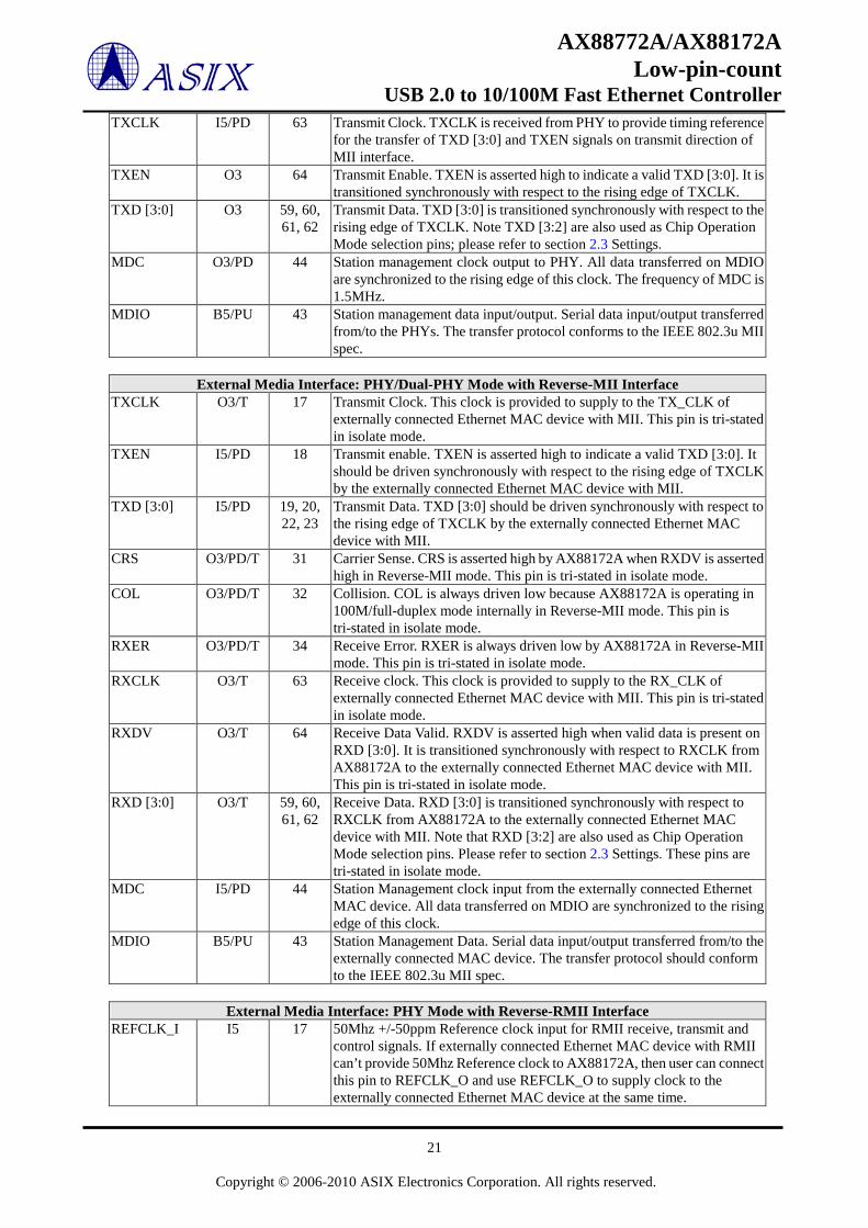
External Media Interface: MAC Mode with MII Interface RXCLK I5/PD 17 Receive Clock. RXCLK is received from PHY to provide timing reference
for the transfer of RXD [3:0] and RXDV signals on receive direction of MII interface.
RXDV I5/PD 18 Receive Data Valid. RXDV is asserted high when valid data is present on RXD [3:0]. It is driven synchronously with respect to RXCLK by PHY.
RXD [3:0] I5/PD 19, 20, 22, 23
Receive Data. RXD [3:0] is driven synchronously with respect to RXCLK by PHY.
CRS I5/PD 31 Carrier Sense. CRS is asserted high asynchronously by the PHY when either transmit or receive medium is non-idle.
COL I5/PD 32 Collision. COL is driven high by PHY when the collision is detected.
TXCLK I5/PD 63 Transmit Clock. TXCLK is received from PHY to provide timing reference for the transfer of TXD [3:0] and TXEN signals on transmit direction of MII interface.
TXEN O3 64 Transmit Enable. TXEN is asserted high to indicate a valid TXD [3:0]. It is transitioned synchronously with respect to the rising edge of TXCLK.
TXD [3:0] O3 59, 60, 61, 62
Transmit Data. TXD [3:0] is transitioned synchronously with respect to the rising edge of TXCLK. Note TXD [3:2] are also used as Chip Operation Mode selection pins; please refer to section 2.3 Settings.
MDC O3/PD 44 Station management clock output to PHY. All data transferred on MDIO are synchronized to the rising edge of this clock. The frequency of MDC is 1.5MHz.
MDIO B5/PU 43 Station management data input/output. Serial data input/output transferred from/to the PHYs. The transfer protocol conforms to the IEEE 802.3u MII spec.
External Media Interface: PHY/Dual-PHY Mode with Reverse-MII Interface
TXCLK O3/T 17 Transmit Clock. This clock is provided to supply to the TX_CLK of externally connected Ethernet MAC device with MII. This pin is tri-stated in isolate mode.
TXEN I5/PD 18 Transmit enable. TXEN is asserted high to indicate a valid TXD [3:0]. It should be driven synchronously with respect to the rising edge of TXCLK by the externally connected Ethernet MAC device with MII.
TXD [3:0] I5/PD 19, 20, 22, 23
Transmit Data. TXD [3:0] should be driven synchronously with respect to the rising edge of TXCLK by the externally connected Ethernet MAC device with MII.
CRS O3/PD/T 31 Carrier Sense. CRS is asserted high by AX88172A when RXDV is asserted high in Reverse-MII mode. This pin is tri-stated in isolate mode.
COL O3/PD/T 32 Collision. COL is always driven low because AX88172A is operating in 100M/full-duplex mode internally in Reverse-MII mode. This pin is tri-stated in isolate mode.
RXER O3/PD/T 34 Receive Error. RXER is always driven low by AX88172A in Reverse-MII mode. This pin is tri-stated in isolate mode.
RXCLK O3/T 63 Receive clock. This clock is provided to supply to the RX_CLK of externally connected Ethernet MAC device with MII. This pin is tri-stated in isolate mode.
RXDV O3/T 64 Receive Data Valid. RXDV is asserted high when valid data is present on RXD [3:0]. It is transitioned synchronously with respect to RXCLK from AX88172A to the externally connected Ethernet MAC device with MII. This pin is tri-stated in isolate mode.
RXD [3:0] O3/T 59, 60, 61, 62
Receive Data. RXD [3:0] is transitioned synchronously with respect to RXCLK from AX88172A to the externally connected Ethernet MAC device with MII. Note that RXD [3:2] are also used as Chip Operation Mode selection pins. Please refer to section 2.3 Settings. These pins are tri-stated in isolate mode.
MDC I5/PD 44 Station Management clock input from the externally connected Ethernet MAC device. All data transferred on MDIO are synchronized to the rising edge of this clock.
MDIO B5/PU 43 Station Management Data. Serial data input/output transferred from/to the externally connected MAC device. The transfer protocol should conform to the IEEE 802.3u MII spec.
External Media Interface: PHY Mode with Reverse-RMII Interface
REFCLK_I I5 17 50Mhz +/-50ppm Reference clock input for RMII receive, transmit and control signals. If externally connected Ethernet MAC device with RMII can’t provide 50Mhz Reference clock to AX88172A, then user can connect this pin to REFCLK_O and use REFCLK_O to supply clock to the externally connected Ethernet MAC device at the same time.
TXEN I5/PD 18 Transmit Enable from the externally connected Ethernet MAC device with RMII.
TXD [1:0] I5/PD 22, 23 Transmit Data from the externally connected Ethernet MAC device with RMII.
NC I5/PD 19, 20 NC NC O3/PD 31, 32 NC RXER O3/PD/T 34 Receive Error. RXER is always driven low by AX88172A in
Reverse-RMII mode. This pin is tri-stated in isolate mode. MIS_1 I5/PD 59 External Media Interface Select 1. This is used as Chip Operation Mode
selection pin; please refer to section 2.3 Settings. MIS_0 I5/PD 60 External Media Interface Select 0. This is used as Chip Operation Mode
selection pin; please refer to section 2.3 Settings. REFCLK_O O3 63 50Mhz Reference clock output. If the externally connected Ethernet MAC
device can’t supply 50Mhz reference clock, this clock can be used to supply to the REF_CLK of externally connected Ethernet MAC device with RMII and the REFCLK_I of this chip.
CRSDV O3/T 64 Carrier Sense and Receive Data Valid to the externally connected Ethernet MAC device with RMII. This pin is tri-stated in isolate mode.
RXD [1:0] O3/T 61, 62 Receive Data to the externally connected Ethernet MAC device with RMII. These pins are tri-stated in isolate mode.
MDC I5/PD 44 Station Management clock input from the externally connected Ethernet MAC device. All data transferred on MDIO are synchronized to the rising edge of this clock.
MDIO B5/PU 43 Station Management Data. Serial data input/output transferred from/to the externally connected MAC device. The transfer protocol should conform to the IEEE 802.3u MII spec.
2.3 Hardware Setting For Operation Mode And Multi-Function Pins The following hardware settings define the desired function or interface modes of operation for some multi-function pins. The logic level shown on setting pin below is loaded from the chip I/O pins during power on reset based on the setting the pin’s pulled-up (as logic ‘1’) or pulled-down (as logic ‘0’) resister on the schematic. Chip Operation Mode setting (applicable to AX88172A only):
Pin# 59, Pin #60 Operation Modes Remarks 00 (default, Note 1) MAC mode Internal PHY When SSEN = 0 in Software Interface Selection register
(6.2.1.24), the Chip Operation Mode is determined by Pin# 59 and Pin #60 value of AX88172A package pinout, which is called hardware setting (see Note 2).
01 External MII 10 Dual-PHY mode Reverse-MII 11 Reserved
Note 1: The Pin# 59 and Pin# 60 settings are only applicable to the AX88172A. The AX88772A always defaults to MAC mode with internal PHY.
Note 2: The SSEN bit defaults to 0 after power on reset, meaning that the hardware setting is used to determine Chip Operation Mode during power on reset. Alternatively, after the AX88172A software driver writes SSEN to 1 during initialization, the Chip Operation Mode can be configured by the Software Interface Selection register vendor command (6.2.1.24).
EECK pin: Force USB to Full Speed mode:
EECK Description 0 Normal operation (default). 1 Force USB to Full Speed mode. External pull-up resistor must be 4.7Kohm.
GPIO_1 pin: Determines whether this chip will go to Default WOL Ready Mode after power on reset. The WOL stands
for Wake-On-LAN.
GPIO_1 Description 1 Enable Default WOL Ready Mode. Notice that the external pulled-up resistor must be 4.7Kohm.
For more details, please refer to APPENDIX A. Default Wake-On-LAN (WOL) Ready Mode. 0 Normal operation mode (default, see Note 3).
Note 3: This is the default with internal pulled-down resistor and doesn’t need an external one. EEPROM Flag [12]: Defines the multi-function pin GPIO_0 / PME GPIO_0 is a general purpose I/O normally controlled by vendor commands. Users can change this pin to operate as a PME (Power Management Event) for remote wake up purpose. Please refer to 4.1.2 Flag of bit 12 (PME_PIN). EEPROM Flag [1]: Defines the function of SI_[3:0] pins to be either SPI or I2C/UART
EEPROM Flag [1] Description
1 SI_[3:0] pins are used as SPI function pin
Pin Name Function Pin Type in Master/Slave Mode SI_0 SPI_SCLK Output / Input SI_1 SPI_SS Output / Input SI_2 SPI_MOSI Output / Input SI_3 SPI_MISO Input / Output
0 SI_[3:0] pins are used as I2C/UART function pin (default)
3.1 USB Core and Interface The USB core and interface contains a USB 2.0 transceiver, serial interface engine (SIE), USB bus protocol handshaking block, USB standard command, vendor command registers, logic for supporting bulk transfer, and an interrupt transfer, etc. The USB interface is used to communicate with a USB host controller and is compliant with USB specification V1.1 and V2.0.
3.2 10/100M Ethernet PHY The 10/100M Fast Ethernet PHY is compliant with IEEE 802.3 and IEEE 802.3u standards. It contains an on-chip crystal oscillator, PLL-based clock multiplier, and a digital phase-locked loop for data/timing recovery. It provides over-sampling mixed-signal transmit drivers compliant with 10/100BASE-TX transmit wave shaping / slew rate control requirements. It has a robust mixed-signal loop adaptive equalizer for receiving signal recovery. It contains a baseline wander corrective block to compensate data dependent offset due to AC coupling transformers. It supports auto-negotiation and auto-MDIX functions.
3.3 MAC Core The MAC core supports 802.3 and 802.3u MAC sub-layer functions, such as basic MAC frame receive and transmit, CRC checking and generation, filtering, forwarding, flow-control in full-duplex mode, and collision-detection and handling in half-duplex mode, etc. It provides a media-independent interface (MII) for implementing Fast Ethernet and HomePNA functions. The MAC core interfaces to external MII, Reverse-MII, Reverse-RMII interface I/O pins and MII interface of the embedded 10/100M Ethernet PHY. The selection among the interfaces is done via setting Pin# 59 and Pin #60 of AX88172A package pinout during power on reset (see 2.3) or using the USB vendor command, Software Interface Selection register (see 6.2.1.24). Figure 10 shows the data path diagram of 10/100M Ethernet PHY and MII, Reverse-MII, Reverse-RMII interface to MAC core.
Figure 12 : Internal Data path Diagram of 10/100M Ethernet PHY and MII Interface
3.4 Operation Mode For simple USB 2.0 to Ethernet applications, user can use the AX88772A, which operates with internal Ethernet PHY. For more complex applications that require the use of the External Media Interface (MII, Reverse-MII or Reverse-RMII), users should choose the AX88172A. In this case, AX88172A supports following three operation modes: (Ref. 2.3 Hardware Setting For Operation Mode And Multi-Function Pins)
1. MAC mode 2. PHY mode 3. Dual-PHY mode
Below provides a detailed description for the three operation modes: In MAC mode, the AX88172A Ethernet block is configured as an Ethernet MAC. From a system application
standpoint, AX88172A can be used as a USB 2.0 to LAN Adaptor (see Figure 2) or a USB 2.0 to Fast Ethernet and 100BASE-FX Fiber/HomePNA Combo (see Figure 3).
In MAC mode, the AX88172A internal datapath can work with internal Ethernet PHY or MII interface by selecting between the two via the USB vendor command, Software Interface Selection Register (SSEN). Please refer to Table 10 for the external MII interface selection table. Note that the PHY_ID for the internal Ethernet PHY and external one are defined in Table 3.
In PHY mode, the AX88172A Ethernet block is configured as an Ethernet PHY interface. In this case, an external
microcontroller with Ethernet MAC can interface with AX88172A as if it were to interface with an Ethernet PHY chip, and AX88172A can act as a USB to Reverse-MII/RMII bridge chip for the microcontroller to provide USB 2.0 device interface for some system applications (see Figure 4).
In PHY mode, the AX88172A internal datapath can work with the internal Ethernet PHY or the external Reverse-MII or Reverse-RMII interface by selecting between the two via the USB vendor command, Software Interface Selection Register (SSEN). Please refer to Table 10 for external Reverse-MII or Reverse-RMII interface selection table. Note that the PHY_ID for the internal Ethernet PHY and external one are defined in Table 3.
In Dual-PHY mode, the AX88172A Ethernet block is configured as a dual Ethernet PHY-like interface. In this
case, an external micro controller with Ethernet MAC can interface with the AX88172A as if it were interfacing with two Ethernet PHY chips. The “Dual-PHY Mode” name comes from allowing the external Ethernet MAC to use AX88172A’s internal Ethernet PHY as a regular Ethernet PHY chip for one mode or use AX88172A’s internal USB to MII bridging engine as an Reverse-MII to USB 2.0 bridge chip for another mode.
This Dual-PHY mode provides the external Ethernet MAC device with a cost effective Ethernet PHY and USB 2.0 (PHY) device interface in a single chip for the system applications that need both an Ethernet port and a USB 2.0 port (see Figure 6) through the same Reverse-MII interface and two sets of Station Management registers (as described in section 7 and section 8).
In Dual-PHY mode, the external Ethernet MAC device can work with internal Ethernet PHY or internal USB to MII bridging engine by selecting between the two via PHY Mode Control Register (PM_Control). Please refer to Table 10 for the external Reverse-MII interface selection table. Note that the PHY_ID for the internal Ethernet PHY and internal USB to MII bridging engine are defined in Table 3.
3.5 Station Management (STA) The Station Management interface provides a simple, two-wire, serial interface to connect to a managed PHY device for the purpose of controlling the PHY and gathering status from the PHY. The Station Management interface allows communicating with multiple PHY devices at the same time by identifying the managed PHY with 5-bit, unique PHY_ID. The PHY ID of the embedded 10/100M Ethernet PHY is being pre-assigned to “1_0000”. The Figure 17 shows the internal control MUX of the Station Management interface when doing read in MAC operation mode, the “mdin” signal will be driven from the embedded 10/100M Ethernet PHY only if PHY ID matches with “1_0000”, otherwise, it will always be driven from the external MDIO pin of the ASIC. The Station Management unit also reports the basic PHY status when operating in PHY mode acting as a PHY role (see Figure 18) or in Dual-PHY mode (see Figure 19). For detailed register description, please refer to the Station Management Registers in PHY/Dual-PHYmode (8.0).
Figure 17 : Internal Control MUX of Station Management Interface in MAC mode
MDC
MDIO
Station Management accessed from USB Vendor Command
Figure 18 : Internal Control MUX of Station Management Interface in PHY mode
Note: In Dual-PHY mode, the external Ethernet MAC device will see two sets of Station Management Registers available for access. The USB vendor command will be prohibited from accessing the embedded Ethernet PHY register.
Figure 19 : Internal Control MUX of Station Management Interface in Dual-PHY mode
Station Management accessed from USB Vendor Command
Embedded 10/100M Ethernet PHY
PHY_ID = 1_0000 (Registers refer to Table 16)
mdin
mdout
MDIO
MDC
mdc
Fixed to ‘1’
Station Management to be accessed through EMI in PHY
mode PHY ID = {Secondary
PHY_ID [4:1], 0} (Registers refer to Table 17)
PM_mdc
PM_mdout
PM_mdin
Station Management accessed from USB Vendor Command
3.6 Memory Arbiter The memory arbiter block is responsible for storing received MAC frames into on-chip SRAM (packet buffer) and then forwarding it to the USB bus upon request from the USB host via Bulk In transfer. It also monitors the packet buffer usage in full-duplex mode for triggering PAUSE frame (or in half-duplex mode to activate Backpressure jam signal) transmission out on TX direction. The memory arbiter block is also responsible for storing MAC frames received from the USB host via Bulk Out transfer and scheduling transmission out towards Ethernet network.
3.7 USB to Ethernet Bridge The USB to Ethernet bridge block is responsible for converting Ethernet MAC frame into USB packets or vice-versa. This block supports proprietary burst transfer mechanism (US Patent Approval) to offload software burden and to offer very high packet transfer throughput over USB bus.
3.8 Serial EEPROM Loader The serial EEPROM loader is responsible for reading configuration data automatically from the external serial EEPROM after power-on reset. If the content of EEPROM offset 0x00 (first word) is 0x0000 or 0xFFFF, the Serial EEPROM Loader will not auto-load the EEPROM. In that case, the chip internal default value will be used to configure the chip operation setting and to respond to USB commands, etc.
3.9 General Purpose I/O There are 3 general-purpose I/O pins named GPIO_0/1/2 provided by this ASIC.
3.10 Serial Interface Controller There are 3 serial interfaces provided by the AX88772A/172A: UART, I2C, and SPI. The UART/I2C and SPI share the same pins. Please refer to section 2.3 EEPROM Flag [1] setting. The UART function uses 2 wires, UART_TX and UART_RX, for interfacing with an external RS-232 transceiver. To simplify the serial interface (just 2 wires), there is no hardware flow control signal (like CTS, RTS, DSR, DTR, etc) supported. The main features of UART are listed below:
The UART can support up to 19200 bps full duplex in USB High Speed mode. Note: 38400/57600 bps only for TXD.
The UART has a 24-byte deep transmit FIFO and a 16-byte deep receive FIFO. Fully programmable serial interface
Even, odd, no parity bit generation and detection 5, 6, 7, 8 data bit 1, 1.5, 2 stop bit generation
The I2C controller supports Standard-mode (100K bps) and Fast-mode (400K bps), but not High-speed mode (3.4M bps) of standard I2C bus specs. With 2 wires: I2C_SCL, I2C_SDA, the I2C controller consists of an I2C master controller to support communication to external I2C devices (as Slaves), and an I2C slave controller to support communication to external micro-controller with I2C master. The Serial Peripheral Interface (SPI) controller provides a full-duplex, synchronous serial communication interface (4 wires: SPI_SCLK, SPI_SS, SPI_MOSI, SPI_MISO) to flexibly work with numerous peripheral devices or microcontroller with SPI. The SPI controller consists of a SPI master controller with a slave select pin, SPI_SS to connect to a SPI device, and a SPI slave controller to support communication with external microcontroller with SPI master.
By using the command structure defined in the Command Block Wrapper for Serial Interface (6.2.2), which is based on Endpoint 4 (Bulk In type) and Endpoint 5 (Bulk Out type), the serial data can be transmitted from USB Host Controller to Serial Interface block to generate UART-TX, I2C/SPI Master mode write access, and I2C/SPI Slave mode read access on I2C/SPI bus timing. When receiving data from UART_RX, I2C/SPI Master mode read access and I2C/SPI Slave mode write access from Serial Interface block, the received data can be returned to the USB Host Controller via the Command Block Wrapper structure as well.
3.11 Clock Generation
The AX88772A/AX88172A integrates two internal oscillator circuits for 25Mhz and 12Mhz, respectively, which allow the chip to operate cost effectively with just external 25Mhz and 12Mhz crystals. There are also three PLL circuits integrated in the chip to generate precise clocks. The external 12Mhz crystal or oscillator, via pins XTL12P/XTL12N, provides the reference clock to one of the internal PLL circuit to generate clocks for the embedded USB PHY operation and also a 60Mhz clock source for the internal USB SIE interface. The other 25Mhz crystal or oscillator, via pins XTL25P/XTL25N, provides the reference clock to the other two internal PLL circuit to generate a free-run 100Mhz clock source for the PHY/Dual-PHY mode of AX88172A and a 125Mhz clock source for the embedded Ethernet PHY use. The AX88172A can provide RXCLK and TXCLK (25Mhz output) in Reverse-MII mode or REFCLK_O (50Mhz output) in Reverse-RMII mode. These output clocks are derived from the internal 100Mhz PLL circuit. The external 25Mhz and 12Mhz Crystal Units spec are listed in below table. For more details on crystal timing, please refer to 9.4.1 Clock Timing and AX88x72A Demo board schematic reference.
Parameter Symbol Typical Value Nominal Frequency Fo
12.000000MHz
25.000000MHz
Oscillation Mode Fundamental
Frequency Tolerance(@25℃) ±30ppm
Operation Temperature Range 0℃ ~ +70℃
Aging ±3ppm/year
Table 4 : The external 25Mhz and 12Mhz Crystal Units specifications
To implement the external circuits of 12/25MHz crystal please refer to below. One external 1Mohm resistor on 25MHz crystal oscillator is required.
Figure 20 : One external 1M ohm resistor on 25MHz crystal oscillator is necessary
Conversely, for the 25MHz oscillator, its feedback resistor Rf isn’t integrated into the 25MHz oscillator, so it is necessary to add feedback resistor on external circuit.
XTL25P XTL25N
25MHz
12MHz
XTL12P XTL12N
The left side figure shows one possible implementation of the oscillator on AX88772A/AX88172A device. The feedback resistor Rf has been integrated into the 12MHz oscillator pad internal to AX88772A/AX88172A. This resistor is used to provide DC bias to a CMOS inverter for inversion amplifier operation. 1M Ohms is selected for its optimal bias. Notice that: it is not necessary to add feedback resistor on external circuit.
The AX88772A/AX88172A integrates an internal power-on-reset circuit, which can simplify the external reset circuitry on PCB design. The power-on-reset circuit generates a reset pulse to reset system logic after 1.8V core power ramping up to 1.2V (typical threshold). The external hardware reset input pin, RESET_N, is fed directly to the input of the power-on-reset circuit and can also be used as additional hardware reset source to reset the system logic. For more details on RESET_N timing, please refer to 9.4.2 Reset Timing.
3.13 Voltage Regulator
The AX88772A/AX88172A contains an internal 3.3V to 1.8V low-dropout-voltage and low-standby-current voltage regulator. The internal regulator provides up to 240mA of driving current for the 1.8V core/analog power of the chip to satisfy the worst-case power consumption scenario. Also, for the purpose of lowering power consumption before USB configuration, the internal regulator can operate in standby mode to consume less current when the required driving current is less than 30mA. For more details on voltage regulator DC characteristic, please refer to 9.1.6 DC Characteristics of Voltage Regulator.
4.1 Detailed Description The following sections provide detailed descriptions for some of the fields in serial EEPROM memory map. For other fields not covered here, please refer to the AX88x72A EEPROM User Guide for more details.
4.1.1 Word Count for Preload (00h) The number of words to be preloaded by the EEPROM loader = 15h.
4.1.2 Flag (01h)
Bit 15 Bit 14 Bit 13 Bit 12 Bit 11 Bit 10 Bit 9 Bit 8 PME_IND PME_TYP PME_POL PME_PIN PHY_ISO Reserved TDPE CEM
Bit 7 Bit 6 Bit 5 Bit 4 Bit 3 Bit 2 Bit 1 Bit 0 TACE RDCE SCPR CBW_EN GPIO2_PM RWU SPI_en SP
SP: Self-Power (for USB standard command Get Status) 1: Self power. (Note: The Dual-PHY mode is only allowed to operate under this self power condition.) 0: Bus power (default). SPI_en: SPI enable 1: SPI enable. Enable SI_0 ~ SI_3 pins as SPI function. 0: UART & I2C enable. Enable SI_0 ~ SI_3 pins as UART and I2C function (default). RWU: Remote Wakeup support.
1: Indicate that this device supports Remote Wakeup (default). 0: Not support.
GPIO2_PM: GPIO_2 function in PHY/Dual-PHY mode 1: RXER (default). 0: GPIO_2.
CBW_EN: Enable the two bulk-type endpoints for CBW 1: Enable (default). 0: Disable.
SCPR: Software Control PHY Reset. 1: IPRL bit in Vendor command Software Reset Register (20h) resets the embedded Ethernet PHY (default). 0: The USB_Reset on USB bus resets the embedded Ethernet PHY. RDCE: RX Drop CRC Enable. 1: CRC byte is dropped on received MAC frame forwarding to host (default). 0: CRC byte is not dropped. TACE: TX Append CRC Enable. 1: CRC byte is generated and appended by the ASIC for every transmitted MAC frame (default). 0: CRC byte is not appended. CEM: Capture Effective Mode. 1: Capture effective mode enable (default). 0: Disabled. TDPE: Test Debug Port Enable. 1: Enable test debug port for chip debug purpose. 0: Disable test debug port and the chip operate in normal function mode (default). PHY_ISO: Set MII bus to isolate mode when operating in PHY mode. 1: Set MII bus to isolate mode (default). AX88172A can be in isolate mode when operating in PHY mode with
Reverse-MII/RMII. Following output pins are tri-stated in isolate mode. In Reverse-MII mode: RXD [3:0], CRS, RXDV, RXCLK, RXER, COL and TXCLK.
In Reverse-RMII mode: RXD [1:0] and CRSDV, RXER, except for REFCLK_O. 0: Set MII bus to non-isolate mode.
1: Set GPIO_0 pin as PME (default). 0: GPIO_0 pin is controlled by vendor command.
PME_POL: PME pin active Polarity. 1: PME active high.
0: PME active low (default). PME_TYP: PME I/O Type.
1: PME output is a Push-Pull driver. 0: PME output to function as an open-drain buffer (default).
PME_IND: PME indication. 1: An 1.363ms pulse active when detecting wake-up event.
0: A static signal active when detecting wake-up event (default).
4.1.3 Node ID (04~06h) The Node ID 0 to 5 bytes represent the MAC address of the device, for example, if MAC address = 01-23-45-67-89-ABh, then Node ID 0 = 01, Node ID 1 = 23, Node ID 2 = 45, Node ID 3 = 67, Node ID 4 = 89, and Node ID 5 = AB. Default values: Node ID {0,1,2,3,4,5} = 0x000E_C687_7201.
4.1.4 PHY Register Offset for Interrupt Endpoint (0Fh)
Bit 15 Bit 14 Bit 13 Bit 12 Bit 11 Bit 10 Bit 9 Bit 8 EtherPhyMode PHY Register Offset 1
Bit 7 Bit 6 Bit 5 Bit 4 Bit 3 Bit 2 Bit 1 Bit 0 100 PHY Register Offset 2
PHY Register Offset 1: Fill in PHY’s Register Offset of Primary PHY here. Upon each Interrupt Endpoint issued, its
register value will be reported in byte# 5 and 6 of Interrupt Endpoint packet (default = 00101) PHY Register Offset 2: Fill in PHY’s Register Offset of Primary PHY here. Upon each Interrupt Endpoint issued, its
register value will be reported in byte# 7 and 8 of Interrupt Endpoint packet (default = 11100)
EtherPhyMode: as below table (default = 000),
EtherPhyMode [2:0] Function 000 Auto-negotiation enable with all capabilities 001 Auto-negotiation with 100BASE-TX FDX / HDX ability 010 Auto-negotiation with 10BASE-TX FDX / HDX ability 011 Reserved 100 Manual selection of 100BASE-TX FDX
101 Manual selection of 100BASE-TX HDX 110 Manual selection of 10BASE-T FDX 111 Manual selection of 10BASE-T HDX
Note: 1. EtherPhyMode is used to set the operation mode of embedded Ethernet PHY directly. For normal operation
mode, set them to 000. 2. This value is latched into embedded Ethernet PHY right after it leaves reset. After that, software driver can
still make change Ethernet PHY link ability through vendor command PHY Write Register to access embedded Ethernet PHY register.
Fill the maximum RX/TX MAC frame size supported by this ASIC. The number must be even number in terms of bytes and should be less than or equal to 2500 bytes (default = 0600h).
4.1.6 Primary/Secondary PHY_Type and PHY_ID (11h) The 3 bits PHY_Type field for both Primary and Secondary PHY is defined as follows,
000: 10/100M Ethernet PHY or 1M HomePNA PHY. 111: non-supported PHY. For example, the High Byte value of “E0h” means that secondary PHY is not supported.
Default values: Primary {PHY_Type, PHY_ID} = 10h. Secondary {PHY_Type, PHY_ID} = E0h. Note that the PHY_ID of the embedded 10/100M Ethernet PHY is being assigned to “10h”. Secondary PHY_ID always defines The PHY_ID of External Media Interface (EMI) and Secondary PHY_TYPE is not used in that case. Please refer to Table 3 for more information.
4.1.7 Pause Frame Free Buffers High Water and Low Water Mark (12H) When operating in full-duplex mode, correct setting of this field is very important and can affect the overall packet receive throughput performance a great deal. The High Water Mark is the threshold to trigger sending Pause frame and the Low Water Mark is the threshold to stop sending Pause frame. Note that each free buffer count here represents 128 bytes of packet storage space in SRAM. These setting values are also used in half-duplex mode to activate Backpressure to send /stop jam signal.
Figure 21 : Water level setting for flow control
4.1.8 Power-Up Steps After power-on reset, AX88772A/AX88172A will automatically perform the following steps to the Ethernet PHYs via MDC/MDIO lines (only take effect when Chip Operation Mode is in MAC mode with external PHY on MII interface).
1. Write to PHY_ID of 00h with PHY register offset 00h to power down all PHYs attached to station management interface.
2. Write to Primary PHY_ID with PHY register offset 00h to power down Primary PHY. 3. Write to Secondary PHY_ID with PHY register offset 00h to power down Secondary PHY.
Notice that enabling Default WOL Ready Mode (see 2.3 GPIO_1 Settings) will disable above power-up step (to prevent external Ethernet PHY on MII interface from entering power-down mode, if external PHY is used).
Total free buffer count = 128
Start sending Pause frame when free buffer < High Water Mark (default = 24h)
Total free buffer count = 0
Stop sending Pause frame when free buffer > Low Water Mark (default = 42h)
5.1 USB Configuration The AX88772A/AX88172A supports 1 Configuration only.
5.2 USB Interface The AX88772A/AX88172A supports 1 interface.
5.3 USB Endpoints The AX88772A/AX88172A supports following 4 or 6 endpoints: Endpoint 0: Control endpoint. It is used for configuring the device. Please refer to USB Standard Commands (6.1) and
USB Vendor Commands (6.2), etc. Endpoint 1: Interrupt endpoint. It is used for reporting status. Please refer to Interrupt Endpoint (6.3). Endpoint 2: Bulk In endpoint. It is used for receiving Ethernet Packet. Endpoint 3: Bulk Out endpoint. It is used for transmitting Ethernet Packet. Endpoint 4: Optional Bulk In endpoint. It is used for receiving CBW frame. Please refer to Command Block Wrapper
for Serial Interface (6.2.2). Endpoint 5: Optional Bulk Out endpoint. It is used for transmitting CBW frame. Please refer to Command Block
Wrapper for Serial Interface (6.2.2). Note that CBW_EN bit in EEPROM Flag [4] (4.1.2) is used to enable Endpoint 4 and Endpoint 5.
6.0 USB Commands There are three command groups for Endpoint 0 (Control Endpoint) in AX88772A/AX88172A: The USB standard commands The USB vendor commands The USB Communication Class commands
6.1 USB Standard Commands The Language ID is 0x0904 for English PPLL means buffer length CC means configuration number I I means Interface number AA means Device Address
Setup Command Data Bytes Access Type Description
8006_00 01 00 00 LLPP PPLL bytes in Data stage Read Get Device Descriptor
8006_0002 0000_LLPP PPLL bytes in Data stage Read Get Configuration Descriptor
8006_0003_0000_LLPP PPLL bytes in Data stage Read Get Supported Language ID
8006_0103_0904_LLPP PPLL bytes in Data stage Read Get Manufacture String
8006_0203_0904_LLPP PPLL bytes in Data stage Read Get Product String
8006_0303_0904_LLPP PPLL bytes in Data stage Read Get Serial Number String
8006_0403_0904_LLPP PPLL bytes in Data stage Read Get Configuration String
8006_0503_0904_LLPP PPLL bytes in Data stage Read Get Interface 0 String
8006_0603_0904_LLPP PPLL bytes in Data stage Read Get Interface 1/0 String
8006_0703_0904_LLPP PPLL bytes in Data stage Read Get Interface 1/1 String
8008_0000_0000_0100 1 bytes in Data stage Read Get Configuration
0009_CC00_0000_0000 No data in Data stage Write Set Configuration
810A_0000 _I I00_0100 1 bytes in Data stage Read Get Interface
010B_AS00_0000_0000 No data in Data stage Write Set Interface
0005_AA00_0000_0000 No data in Data stage Write Set Address
6.2 USB Vendor Commands AA, CC: The index of register or the content of register. BB, DD: The content of register
No Setup Command Data Bytes Access Type Description 1 C002_AA0B_0C00_0800 8 bytes in Data stage Read Rx/Tx SRAM Read Register 2 4003_AA0B_0C00_0800 8 bytes in Data stage Write Rx/Tx SRAM Write Register 3 4006_0000_0000_0000 No data in Data stage Write Software Station Management Control
Register 4 C007_ AA00_CC00_0200 2 bytes in Data stage Read PHY Read Register 5 4008 _AA00_CC00_0200 2 bytes in Data stage Write PHY Write Register 6 C009_0000_0000_0100 1 bytes in Data stage Read Station Management Status Register 7 400A_0000_0000_0000 No data in Data stage Write Hardware Station Management Control
Register 8 C00B_AA00_0000_0200 2 bytes in Data stage Read SROM Read Register 9 400C_AA00_CCDD_0000 No data in Data stage Write SROM Write Register 10 400D_0000_0000_0000 No data in Data stage Write SROM Write Enable Register 11 400E_0000_0000_0000 No data in Data stage Write SROM Write Disable Register 12 C00F_0000_0000_0200 2 bytes in Data stage Read Rx Control Register 13 4010_AABB_0000_0000 No data in Data stage Write Rx Control Register 14 C011_0000_0000_0300 3 bytes in Data stage Read IPG/IPG1/IPG2 Register 15 4012_AABB_CC00_0000 No data in Data stage Write IPG/IPG1/IPG2 Register 16 C013_0000_0000_0600 6 bytes in Data stage Read Node ID Register 17 4014_0000_0000_0600 6 bytes in Data stage Write Node ID Register 18 C015_0000_0000_0800 8 bytes, MA0~MA7, in
Data stage Read Multicast Filter Array Register
19 4016_0000_0000_0800 8 bytes, MA0~MA7, in Data stage
Write Multicast Filter Array Register
20 4017_AA00_0000_0000 No data in Data stage Write Test Register 21 C019_0000_0000_0200 2 bytes in Data stage Read Ethernet/HomePNA PHY Address
Register 22 C01A_0000_0000_0200 2 bytes in Data stage Read Medium Status Register 23 401B_AABB_0000 _0000 No data in Data stage Write Medium Mode Register 24 C01C_0000_0000_0100 1 bytes in Data stage Read Monitor Mode Status Register 25 401D_AA00_0000_0000 No data in Data stage Write Monitor Mode Register 26 C01E_0000_0000_0100 1 bytes in Data stage Read GPIOs Status Register 27 401F_AA00_0000_0000 No data in Data stage Write GPIOs Register 28 4020_AA00_0000_0000 No data in Data stage Write Software Reset Register 29 C021_0000_0000_0100 1 bytes in Data stage Read Software Interface Selection Status
Register 30 4022_AA00_0000_0000 No data in Data stage Write Software Interface Selection Register 31 C023_AA00_0000_0400 4 bytes, Wake Up
Register in Data stage Read Wake-up Frame Array Register
32 4024_AA00_0000_0400 4 bytes, Wake Up Register in Data stage
Write Wake-up Frame Array Register
33 C025_0000_0000_0100 1 bytes in Data stage Read Jam Limit Count Register 34 4026_AA00_0000_0000 No data in Data stage Write Jam Limit Count Register 35 C027_0000_0000_0400 4 bytes in Data stage Read VLAN Control Register 36 4028_AABB_CCDD_0000 No data in Data stage Write VLAN Control Register
0h C [3:0] DD [7:0] in Data stage EE [7:0] in Data stage FF [7:0] in Data stage GG [7:0] in Data stage HH [7:0] in Data stage II [7:0] in Data stage JJ [7:0] in Data stage
KK [7:0] in Data stage
{B [3:0], AA [7:0]}: The read address of RX or TX SRAM. C [0]: RAM selection. 0: indicates to read from RX SRAM. 1: indicates to read from TX SRAM. C [3:1]: Reserved.
{DD [7:0], EE [7:0], FF [7:0], GG [7:0], HH [7:0], II [7:0], JJ [7:0], KK [7:0]}: The 64-bits of data presented in Data stage are the data to be written to RX or TX SRAM.
DD [7:0] in Data stage EE [7:0] in Data stage FF [7:0] in Data stage GG [7:0] in Data stage HH [7:0] in Data stage II [7:0] in Data stage JJ [7:0] in Data stage
KK [7:0] in Data stage
{B [3:0], AA [7:0]}: The write address of RX or TX SRAM. C [0]: RAM selection. 0: indicates to write to RX SRAM. 1: indicates to write to TX SRAM. C [3:1]: Reserved. {DD [7:0], EE [7:0], FF [7:0], GG [7:0], HH [7:0], II [7:0], JJ [7:0], KK [7:0]}: The 64-bits of data presented in Data
stage are the data to be written to RX or TX SRAM.
6.2.1.3 Software Station Management Control Register (06h, write only)
When software needs to access to Ethernet PHY’s internal registers, it needs to first issue this command to request the ownership of Station Management Interface. Reading Station Management Status Register can check the ownership status of the interface.
6.2.1.4 PHY Read Register (07h, read only)
Bit7 Bit6 Bit5 Bit4 Bit3 Bit2 Bit1 Bit0 AA [7:0]
00h CC [7:0]
AA [4:0]: The PHY ID value. CC [4:0]: The register address of Ethernet PHY’s internal register. AA [7:5]: Reserved CC [7:5]: Reserved
6.2.1.5 PHY Write Register (08h, write only)
Bit7 Bit6 Bit5 Bit4 Bit3 Bit2 Bit1 Bit0 AA [7:0]
00h CC [7:0]
AA [4:0]: The PHY ID value. CC [4:0]: The register address of Ethernet PHY’s internal register. AA [7:5]: Reserved CC [7:5]: Reserved
6.2.1.6 Station Management Status Register (09h, read only)
6.2.1.7 Hardware Station Management Control Register (0Ah, write only)
When software is done accessing Station Management Interface, it needs to issue this command to release the ownership of the Interface back to ASIC’s hardware. After issuing this command, subsequent PHY Read Register or PHY Write Register from software will be ignored. Notice that Software should issue this command every time after it finishes accessing the Station Management Interface to release the ownership back to hardware to allow periodic Interrupt Endpoint to be able to access the Ethernet PHY’s registers via the Station Management Interface.
6.2.1.8 SROM Read Register (0Bh, read only)
Bit7 Bit6 Bit5 Bit4 Bit3 Bit2 Bit1 Bit0 AA [7:0]
AA [7:0]: The read address of Serial EEROM.
6.2.1.9 SROM Write Register (0Ch, write only)
Bit7 Bit6 Bit5 Bit4 Bit3 Bit2 Bit1 Bit0 AA [7:0]
00h CC [7:0] DD [7:0]
AA [7:0]: The write address of Serial EEROM. {DD [7:0], CC [7:0]}: The write data value of Serial EEROM
6.2.1.10 Write SROM Enable (0Dh, write only) User issues this command to enable write permission to Serial EEPROM from SROM Write Register.
6.2.1.11 Write SROM Disable (0Eh, write only) User issues this command to disable write permission to Serial EEPROM from SROM Write Register.
PRO: PACKET_TYPE_PROMISCUOUS. 1: All frames received by the ASIC are forwarded up toward the host. 0: Disabled (default).
AMALL: PACKET_TYPE_ALL_MULTICAST. 1: All multicast frames received by the ASIC are forwarded up toward the host, not just the frames whose
scrambling result of DA matching with multicast address list provided in Multicast Filter Array Register. 0: Disabled. This only allows multicast frames whose scrambling result of DA field matching with multicast
address list provided in Multicast Filter Array Register to be forwarded up toward the host (default). Bit 2: Please always write 0 to this bit.
AB: PACKET_TYPE_BROADCAST. 1: All broadcast frames received by the ASIC are forwarded up toward the host (default). 0: Disabled.
AM: PACKET_TYPE_MULTICAST. 1: All multicast frames whose scrambling result of DA matching with multicast address list are forwarded up to the
host (default). 0: Disabled.
AP: Accept Physical Address from Multicast Filter Array. 1: Allow unicast packets to be forwarded up toward host if the lookup of scrambling result of DA is found within
multicast address list. 0: Disabled, that is, unicast packets filtering are done without regarding multicast address list (default).
SO: Start Operation. 1: Ethernet MAC start operating. 0: Ethernet MAC stop operating (default).
MFB [1:0]: Maximum Frame Burst transfer on USB bus. 00: 2048 Bytes 01: 4096 Bytes 10: 8192 Bytes 11: 16384 Bytes (default). LPBK: MAC loop back for diagnostic.
1: Enable MAC loopback. 0: Disable MAC loopback (default).
Bit [15:13]: Please always write 0 to these bits.
Following is the truth table about unicast packet filtering condition.
DA Matching Node ID Register?
PRO bit Broadcast or Multicast Packet?
Unicast Packet Filtered by Ethernet MAC?
No 0 No Yes No 1 No No
Yes (see Note below) 0 No No Note: DA Matching Node ID Register including following two cases: 1. Destination Address field of incoming packets matches with Node ID Register. 2. When AP (bit 5) is set to 1and the scrambling result of DA is found within multicast address list.
Following is a truth table about broadcast packet filtering condition.
PRO bit AB bit Broadcast Packet? Broadcast Packet Filtered by Ethernet MAC? 0 1 Yes No 0 0 Yes Yes 1 0/1 Yes No
6.2.1.13 IPG/IPG1/IPG2 Control Register (11h, read only and 12h, write only)
Bit7 Bit6 Bit5 Bit4 Bit3 Bit2 Bit1 Bit0 IPG [7:0]
IPG1 [7:0] IPG2 [7:0]
AA [6:0] = IPG [6:0]. BB [6:0] = IPG1 [6:0]. CC [6:0] = IPG2 [6:0]. IPG [6:0]: Inter Packet Gap for back-to-back transfer on TX direction in MII mode (default = 15h). IPG1 [6:0]: IPG part1 value (default = 0Ch). IPG2 [6:0]: IPG part1 value + part2 value (default = 12h). AA [7]: Reserved. BB [7]: Reserved. CC [7]: Reserved.
6.2.1.14 Node ID Register (13h, read only and 14h, write only)
Bit7 Bit6 Bit5 Bit4 Bit3 Bit2 Bit1 Bit0 AA [7:0] BB [7:0] CC [7:0] DD [7:0] EE [7:0] FF [7:0]
AA [7:0] = Node ID 0. BB [7:0] = Node ID 1. CC [7:0] = Node ID 2. DD [7:0] = Node ID 3. EE [7:0] = Node ID 4. FF [7:0] = Node ID 5.
{FF [7:0], EE [7:0], DD [7:0], CC [7:0], BB [7:0], AA [7:0]} = Ethernet MAC address [47:0] of AX88772A/AX88172A.
address bit map for multicast frame filtering block. For example, see below Figure 22.
Figure 22 : Multicast Filter Example As shown in below figure, the Multicast Filter Array (MFA) provides filtering of multicast addresses hashed through the CRC logic. All Destination Address field are fed through the 32 bits CRC generation logic. As the last bit of the Destination Address field enters the CRC, the 6 most significant bits of the CRC generator are latched. These 6 bits are then decoded by a 1 to 64 decoder to index a unique filter bit (FB0-63) in the Multicast Filter Array. If the filter bit selected is set, the multicast packet is accepted. The system designer should use a program to determine which filter bits to set in the multicast registers. All multicast filter bits that correspond to Multicast Filter Array Registers accepted by the node are then set to one. To accept all multicast packets all of the registers are set to all ones. Note that received Pause Frames are always filtered by Ethernet MAC regardless of MFA setting.
Example: If the accepted multicast packet’s destination address Y is found to hash to the value 32 (0x20), then FB32 in MA4 should be initialized to “1”. This will allow the Ethernet MAC to accept any multicast packet with the destination address Y. Although the hashing algorithm does not guarantee perfect filtering of multicast address, it will perfectly filter up to 64 logical address filters if these addresses are chosen to map into unique locations in the multicast filter. Note: The LSB bit of received packet’s first byte being “1” signifies a Multicast Address.
Following is the truth table about multicast packet filtering condition.
PRO bit AMALL bit AM bit Pass Hashing Algorithm? Multicast Packet Filtered by Ethernet MAC? 0 0 0 0 Yes 0 0 0 1 Yes 0 0 1 0 Yes 0 0 1 1 No 0 1 0/1 0/1 No 1 0/1 0/1 0/1 No
Note: Passing Hashing Algorithm means that the selected bit in MFA of CRC-32 result is set to “1”.
LDRND: To load Random number into MAC’s exponential back-off timer, the user writes a “1” to enable the ASIC to
load a small random number into MAC’s back-off timer to shorten the back-off duration in each retry after collision. This register is used for test purpose. Default value = 0.
SecPhyType, SecPhyID: The Secondary PHY address loaded from serial EEPROM’s offset address 10h. PriPhyType, PriPhyID: The Primarily PHY address loaded from serial EEPROM’s offset address E0h.
Reserved SM SBP Reserved PS RE AA [7:0] = {PF, 0 , TFC, RFC, 0,1, FD, 0}. BB [7:0] = {Reserved, SM, SBP, Reserved, PS, RE}. Bit 0: Please always write 0 to this bit. FD: Full Duplex mode 1: Full Duplex mode (default). 0: Half Duplex mode. Bit 2: Please always write 1 to this bit. Bit 3: Please always write 0 to this bit. RFC: RX Flow Control enable. 1: Enable receiving of pause frame on RX direction during full duplex mode (default).
0: Disabled. TFC: TX Flow Control enable. 1: Enable transmitting pause frame on TX direction during full duplex mode (default).
0: Disabled. Bit 6: Please always write 0 to this bit. PF: Check only “length/type” field for Pause Frame. 1: Enable. Pause frames are identified only based on L/T filed. 0: Disabled. Pause frames are identified based on both DA and L/T fields (default). RE: Receive Enable. 1: Enable RX path of the ASIC. 0: Disabled (default).
PS: Port Speed in MII mode 1: 100 Mbps (default). 0: 10 Mbps.
SBP: Stop Backpressure. 1: When TFC bit = 1, setting this bit enables backpressure on TX direction “continuously” during RX buffer full
condition in half duplex mode. 0: When TFC bit = 1, setting this bit enable backpressure on TX direction “intermittently” during RX buffer full
condition in half duplex mode (default). SM: Super Mac support. 1: Enable Super Mac to shorten exponential back-off time during transmission retrying.
6.2.1.19 Monitor Mode Status Register (1Ch, read only)
Bit7 Bit6 Bit5 Bit4 Bit3 Bit2 Bit1 Bit0
PME_IND PME_TYPE PME_POL US RWWF RWMP RWLU MOM MOM: Monitor Mode 1: Enabled. All received packets will be checked on DA and CRC but not buffered into memory. 0: Disabled (default).
RWLU: Remote Wakeup trigger by Ethernet Link-up. 1: Enabled (default).
0: Disabled. RWMP: Remote Wakeup trigger by Magic Packet.
1: Enabled (default). 0: Disabled.
RWWF: Remote Wakeup trigger by Wake Up Frame. 1: Enabled. 0: Disabled (default).
US: USB Speed. 1: High speed mode.
0: Full speed mode. PME_POL: PME Polarity.
1: PME active high. 0: PME active Low (default).
PME_TYP: PME I/O Type. 1: PME output is a Push-Pull driver. 0: PME output to function as an open-drain buffer.
PME_IND: PME indication. 1: A 1.363ms pulse active when detect wake-up event. 0: A static signal active when detect wake-up event (default).
Reserved RWWF RWMP RWLU MOM MOM: Monitor Mode. 1: Enable. All received packets will be checked on DA and CRC but not buffered into memory. 0: Disable (default).
RWLU: Remote Wakeup trigger by Ethernet Link-up. 1: Enable (default).
0: Disable. RWMP: Remote Wakeup trigger by Magic Packet.
1: Enable (default). 0: Disable.
RWWF: Remote Wakeup trigger by Wake Up Frame. 1: Enable 0: Disable (default). Below describes some Remote Wakeup settings, wakeup events, and expected behavior of AX88772A/AX88172A. After AX88772A/AX88172A enters into suspend mode, either the USB host or AX88772A/AX88172A itself can awake it up and resume back to the original operation mode before it entered suspend. Following truth table shows the chip setting, wakeup event, and device response supported by this ASIC. Note that “X” stands for don’t-care.
Waken
Up by Setting Wakeup Event Device
wakes up RWU bit
of Flag
byte in
EEPROM
Set_Feature
standard
command
RWWF RWMP RWLU GPIO_1
(*) Host
sends
resume
signal
Receiving
a Wakeup
Frame
Receiving
a Magic
Packet
Linkup
detected
On
Primary
PHY
Linkup
detected
On
Secondary
PHY
EXTWAKEU
P_N pin
USB
Host
X X X X X 0 J K Yes
Device 0 0 X X X 0 X X X X X No
Device 1 1 1 0 0 0 Yes Yes
Device 1 1 0 1 0 0 Yes Yes
Device 1 1 0 0 1 0 Yes ** Yes **
Device 1 1 0 0 1 0 Yes ** Yes **
Device 1 1 X X X 0 Low-pulse Yes
Device X 0 0 0 0 1 Yes Yes *** Low-pulse Yes
*: About Default WOL Ready Mode, please refer to section 2.3 GPIO_1 Settings. **: Please refer to below Table 9. ***: It only works in PHY mode and Dual-PHY mode for AX88172A. Please refer to below Table 9.
00b GPI_2 GPO_2_EN GPI_1 GPO_1_EN GPI_0 GPO_0_EN GPO_0_EN: Current level of pin GPIO_0’s output enable.
GPI_0: Input level on GPIO_0 pin when GPIO_0 is as an input pin. GPO_1_EN: Current level of pin GPIO_1’s output enable.
GPI_1: Input level on GPIO_1 pin when GPIO_1 is as an input pin. GPO_2_EN: Current level of pin GPIO_2’s output enable. GPI_2: Input level on GPIO_2 pin when GPIO_2 is as an input pin.
Reserved IPPD IPRL BZ Reserved BZ_TYP RT RR RR: Clear frame length error for Bulk In. 1: set high to clear state. 0: set low to exit clear state (default). RT: Clear frame length error for Bulk Out. 1: set high to enter clear state. 0: set low to exit clear state (default). BZ_TYP: The type of BZ bit. Define BZ bit whether it can auto-clear itself.
1: Disable that BZ auto-clears itself when it force hardware return a Zero-length packet (default). 0: Auto-clears BZ when it force hardware return a Zero-length packet.
BZ: Force Bulk In to return a Zero-length packet. 1: Software can force Bulk In to return a zero-length USB packet. 0: Normal operation mode (default).
IPRL: Internal PHY Reset control. When SCPR bit = 1(EEPROM flag, bit5), this bit acts as reset signal of internal Ethernet PHY. AX88772A/AX88172A software driver can write it to control the internal Ethernet PHY except in Dual-PHY mode. Please refer to below Figure 25.
1: Internal Ethernet PHY is in operating state. 0: Internal Ethernet PHY in reset state (default).
IPPD: Internal Ethernet PHY Power Down control. AX88772A/AX88172A software driver can write it to control the internal Ethernet PHY except in Dual-PHY mode. Please refer to below Figure 25.
1: Internal Ethernet PHY is in power down mode (default). 0: Internal Ethernet PHY is in operating mode. Note: Please refer to APPENDIX B. Ethernet PHY Power and Reset Control for more information about
AX88772A/AX88172A Ethernet PHY Power and Reset control operations.
Figure 25 : Reset and Power-down control Internal Ethernet PHY
PSEL: PHY Select, when ASEL = 0 (manually select the PHY to operate) 1: Select embedded 10/100M Ethernet PHY (default). 0: Select external one from SS [1:0].
ASEL: Auto Select or Manual Select 1: Automatic selection is based on link status of embedded 10/100M Ethernet PHY. If the embedded PHY is in
link-off state and SSEN = 1, the operation mode is determined by SS [1:0]. 0: Manual selection between the internal 10/100M Ethernet PHY and the external one (default).
SS [1:0]: Software Setting. Write to define the operation mode of External Media Interface
00: (invalid) 01: MII interface (default) 10: Reverse-MII 11: Reverse-RMII
Read the current data path selection of Ethernet block or operation mode of External Media Interface. 00: Selected embedded Ethernet PHY 01: Selected MII interface 10: Selected Reverse-MII 11: Selected Reverse-RMII
SSEN: Software Setting Enable. 1: Software setting is active and the Chip Operation mode is determined by below Table 10. 0: Software setting is inactive and the Chip Operation mode is determined by Pin# 59 and Pin #60 of AX88172A
package pinout (default).
SSEN
(Pin # 59, Pin#60) setting
ASEL
PSEL
Internal PHY
link status
SS [1:0]
Ethernet Interface selection result
0 00 X X X XX Internal PHY 0 01 X X X XX MII 0 10 X X X XX Reverse-MII (Dual-PHY mode) 0 11 X X X XX Reserved 1 X 0 0 X 00 Invalid 1 X 0 0 X 01 MII 1 X 0 0 X 10 Reverse-MII (PHY mode) 1 X 0 0 X 11 Reverse-RMII (PHY mode) 1 X 0 1 X XX Internal PHY 1 X 1 X Link OFF 00 Invalid 1 X 1 X Link OFF 01 MII 1 X 1 X Link OFF 10 Reverse-MII (PHY mode) 1 X 1 X Link OFF 11 Reverse-RMII (PHY mode) 1 X 1 X Link ON XX Internal PHY
6.2.1.25 Wake-up Frame Array Register (23h, read only and 24h, write only)
Bit7 Bit6 Bit5 Bit4 Bit3 Bit2 Bit1 Bit0
WUD0 [7:0] WUD1 [7:0] WUD2 [7:0] WUD3 [7:0]
AA: The index (from 0 to 8) of Wake-Up Frame Array Register as shown in left-hand side of below table. {WUD3 [7:0], WUD2 [7:0], WUD1 [7:0], WUD0 [7:0]} = 32-bits wide register as defined in below table.
Table 11 : Wake-up Frame Array Register (WUD3~0) Structure Definition There are four independent sets of wakeup frame filter supported through the above Byte Mask 0~3. Each wakeup frame filter set consists of Byte Mask, Wakeup Frame CRC, Offset, Last Byte and Command registers. Also, if a more complex pattern of Wakeup Frame is needed, user can choose to cascade two filter sets into one (or up to four filter sets into one) through Cascade Command register and define a longer pattern for Wakeup Frame matching. Below is detailed register definition. Byte Mask 0~3: Each set has 32 bits.
The byte mask defines which bytes in the incoming frame will be examined to determine whether or not this is a wake-up frame.
Wakeup Frame 0~3 CRC: Each has 16 bits.
Based on desired wakeup frame patterns, software should calculate CRC-16 and set it here. The value is used to compare with the CRC-16 calculated on the incoming frame on the bytes defined by Byte Mask 0~3. When matched and the Last Byte 0~3 is also matched, then the frame is considered as a valid wakeup frame. CRC-16 Polynomials = X^16 + X^15 + X^2 + 1.
If wakeup frame filters are cascaded, the Wakeup Frame CRC must be cumulatively calculated. The last CRC value is used for verification.
Offset 0~3: Each has 8 bits.
This defines the offset of the first byte in the incoming frame from which the CRC-16 is calculated for the wakeup frame recognition. Each offset value represents two bytes in the frame. For example: The offset value of 0 is the first byte of the incoming frame’s destination address. The offset value of 1 is the 3rd byte of the incoming frame, etc.
Last Byte 0~3: Each has 8 bits.
This 1-byte pattern is used to compare the last masked byte in the incoming frame. The last masked byte is the byte of the last bit mask being 1 in Byte Mask 0~3. A valid wakeup frame shall have match condition on both Wakeup Frame 0~3 CRC and Last Byte 0~3. If wake-up frame filters are cascaded, the Last Byte for the last cascaded wake-up frame filter is used to verify correctness.
Bit 0: Individual Byte Mask enable for Byte Mask 0~3. 1: Enable. 0: Disable.
Bit 1: Destination address (DA) match enable. 1: The DA field of received packet will be compared with the MAC address of AX88772A/AX88172A. When
receiving frame with DA matching Node ID register and the wakeup frame filter is also matched, then the packet is considered as valid wakeup frame.
0: When receiving frame with any DA value and the wakeup frame filter is matched, then the packet is considered as valid wakeup frame.
Bit 2: Multicast address match enable. 1: The DA field of received packet will be examined if it is a multicast frame and compared with the Multicast Filter
Array (see 6.2.1.15). When receiving frame is a multicast frame, meets Multicast Filter Array, and also matches the wakeup frame filter, the packet is considered as valid wakeup frame.
0: When receiving frame with any DA value matches the wakeup frame filter, the packet is considered as valid wakeup frame.
Bit 3: Reserved. Cascade Command: the Bit 16~18 of Wake-up Frame Array Register 8.
Bit16: 1: Byte Mask 1 and Byte Mask 0 are cascaded to become one wake-up frame filter that allows defining up to 64
masked bytes. 0: Byte Mask 1 and Byte Mask 0 are two independent wake-up frame filters for up to 32 masked bytes each.
Bit17: 1: Byte Mask 2 and Byte Mask 1 are cascaded to become one wake-up frame filter that allows defining up to 64
masked bytes. 0: Byte Mask 2 and Byte Mask 1 are two independent wake-up frame filters for up to 32 masked bytes each.
Bit18: 1: Byte Mask 3 and Byte Mask 2 are cascaded to become one wake-up frame filter that allows defining up to 64
masked bytes. 0: Byte Mask 3 and Byte Mask 2 are two independent wake-up frame filters for up to 32 masked bytes each.
Note: (1) If both Bit16 and Bit 17 set ‘1’, Byte Mask 2 and Byte Mask 1 and Byte Mask 0 are cascaded to become one
wake-up frame filter that allows defining up to 96 masked bytes. (2) If both Bit17 and Bit 18 set ‘1’, Byte Mask 3 and Byte Mask 2 and Byte Mask 1 are cascaded to become one
wake-up frame filter that allows defining up to 96 masked bytes. (3) If Bit18 ~ Bit 16 set ‘1’, Byte Mask 3 ~Byte Mask 0 are cascaded to become one wake-up frame filter that
allows defining up to 128 masked bytes maximum.
6.2.1.26 Jam Limit Count Register (25h, read only and 26h write only)
Jam_Limit[5:0]: This is used for flow-control in half-duplex mode, which is based on force collision mechanisms to backpressure transmitting network node. During the force collision backpressure process, the Ethernet MAC will continue counting total collision count. When it has reached the Jam_Limit setting, the Ethernet MAC will stop backpressure to avoid Ethernet HUB from being partitioned (default = 3Fh) due to excessive collision on network link.
6.2.1.27 VLAN Control Register (27h, read only) and (28h, write only)
Bit7 Bit6 Bit5 Bit4 Bit3 Bit2 Bit1 Bit0
VID1 [7:0] Reserved VSO VFE VID1 [11:8]
VID2 [7:0] Reserved VID2 [11:8]
AA [7:0] = {VID1 [7:0]}. BB [7:0] = {Reserved, VSO, VFE, VID1 [11:8]}. CC [7:0] = {VID2 [7:0]}. DD [7:0] = {Reserved, VID2 [11:8]}. VID1 [11:0]: First VLAN ID for filter.
VFE: VLAN filter enable 1: Enable VLAN filter. The VLAN ID field (12 bits) received 802.1q tagged packets, as in the Figure 26 below, which
will be used to compare with VID1 and VID2 setting. If it matches either VID1 or VID2, or its value is equal to all zeros, the received 802.1q tagged packets will be forwarded to the USB Host. Meanwhile, the VSO bit determines whether the VLAN Tag bytes (4 bytes) are stripped off or not during forwarding to the USB Host. Also, if the incoming packets contain no VLAN Tag bytes, they will be forwarded to the USB Host by default. If there is no match between the received 802.1q tagged packets and VID1 and VID2, the packets will be discarded. Please see below Table 12.
Received packet
VID1, VID2
Untagged Tagged
VID=Zero VID= Not zero Zero Forwarded Forwarded Discarded
Not zero Forwarded Forwarded Match: Forwarded No Match: Discarded
Table 12 : VID1, VID2 setting to filter received packet
0: Disable VLAN filter. The received packets with or without 802.1q Tag bytes will always be forwarded to the USB Host (default).
VSO: VLAN Strip off 1: Strip off VLAN Tag (4 bytes) from the incoming packet. 0: Preserve VLAN Tag in the incoming packet (default). VID2 [11:0]: Second VLAN ID for filter. Note that VID1 and VID2 function as two independent VLAN ID filters. Note that to send the packet with VLANID Tag bytes, the software should append VLAN Tag bytes in the transmitted packets.
The CBW (Command Block Wrapper) structure based on endpoint 4 (Bulk In type) and endpoint 5 (Bulk Out type) is used to access to the three interfaces -UART/I2C/SPI. Its construction is described as below: Serial I/O Command Block Wrapper (CBW): A frame containing a command block and associated information. Serial I/O Command Status Wrapper (CSW): A frame containing the status of a command block. Data-Out: Transmitted data from Host to Device whose data length is up to 16 bytes as maximum CBW data limit. Data-In: Received data from Device to Host whose data length is up to 16 bytes as maximum CBW data limit.
CBWSignature [15:0] = {Byte1, Byte0} = 0x5547. This Signature helps to identify this data packet as a CBW. CBWDeviceCode [1:0]: Serial interface device select.
00: Select to access I2C module 01: Select to access UART module 10: Select to access SPI module Others: Reserved
CBWRegAddr [3:0]: Select which register of the serial interface device to be accessed (CBWDeviceCode).
For UART register map, please refer to UART controller (6.2.2.1). For I2C register map: I2C controller (6.2.2.2).
For SPI register s: SPI controller (6.2.2.3). CBWTag [3:0]: A Command Block Tag sent by the host. The device shall echo the contents of this field back to the host in
the CSWTag field of the associated CSW. The CSWTag positively associates a CSW with the corresponding CBW. CBWDir: CBW Direction
1: Data-In from the device to the host. 0: Data-Out from host to the device,
CBWZero: CBW Zero data. It is indicates this transfer without data phase (Data-In, Data_Out). CBWRst: CBW Reset CBWDeviceCode device. Command Status Wrapper
CSWSignature [15:0] = {Byte1, Byte0} = 0x4755. This Signature helps to identify this data packet as a CSW. CBWDeviceCode [1:0]: Echo Serial interface device selected. CSWTag [3:0]: Echo CBWTag. CSWRegAddr [3:0]: Echo CBWRegAddr. CSWStatus [1:0]: Report the success or failure of the command.
The AX88772A/AX88172A provides a simple UART function with 2 wires, UART_TX and UART_RX, for interfacing with an external RS-232 transceiver. To simplify the serial interface (just 2 wires), there is no hardware flow control signal (like CTS, RTS, DSR, DTR, etc) supported. The main features of UART are listed below:
The UART can support up to 19200 bps full duplex in USB High Speed mode. Note: 38400/57600 bps only for TXD.
The UART has a 24-byte deep transmit FIFO and a 16-byte deep receive FIFO. Fully programmable serial interface
Even, odd, no parity bit generation and detection 5, 6, 7, 8 data bit 1, 1.5, 2 stop bit generation
Line Control Register LCR [7:0] = {0, BCB, SPB, EPS, PE, NSB, NBPC}
NBPC: The number of bits per character in each transmitted or received serial character. 11: 8 bits. 10: 7 bits 01: 6 bits 00: 5 bits
NSB: Specify the number of generated stop bits. Note that the receiver always checks the first stop bit only. 1: 1.5 stop bits when 5-bit character length selected and 2 bits otherwise 0: 1 stop bit
PE: Parity Enable 1: Parity bit is generated on each outgoing character and is checked on each incoming one. 0: No parity
EPS: Even Parity select 1: Even number of ‘1’ is transmitted in each word. 0: Odd number of ‘1’ is transmitted and checked in each word (data and parity combined). In other words, if the
data has an even number of ‘1’ in it, then the parity bit is ‘1’. SPB: Stick Parity bit
1: If bits 3 and 4 are logic ‘1’, the parity bit is transmitted and checked as logic ‘0’. If bit 3 is ‘1’ and bit 4 is ‘0’ then the parity bit is transmitted and checked as ‘1’.
0: Stick Parity disabled BCB: Break Control bit
1: the serial out is forced into logic ‘0’ (break state). 0: break is disabled
IER [4:0] = {WER, MSI, RLSI, THRI, RDI}
RDI: Received Data available interrupt 1: Enable 0: Disable
FIFOE: This UART only supports FIFO mode, so always write 1 to this bit. RFR: Writing ‘1’ to this bit clears the Receiver FIFO and resets its logic. But it doesn’t clear the shift register, i.e.
receiving of the current character continues. TFR: Writing ‘1’ to this bit clears the Transmitter FIFO and resets its logic. The shift register is not cleared, i.e.
transmitting of the current character continues FITL: FIFO Trigger level: Define the Receiver FIFO interrupt level
Timeout Indication There’s at least 1 character in the FIFO but no character has been input to the FIFO or read from it for the last 4 Char times
Reading from the FIFO (Receiver Buffer Register)
0 0 1 0 3rd Transmitter Holding Register empty
Transmitter Holding Register Empty
Writing to the Transmitter Holding Register or reading IIR
0 0 0 0 4th Modem Status CTS, DSR, RI or DCD Reading the Modem status register
Line Status Register LSR [7:0]: {FERR, TEMT, THRE, BI, FE, PE, OE, DR}
DR: Data Ready (DR) indicator. 1: At least one character has been received and is in the FIFO. 0: No characters in the FIFO
OE: Overrun Error (OE) indicator 1: If the FIFO is full and another character has been received in the receiver shift register. If another character is
starting to arrive, it will overwrite the data in the shift register but the FIFO will remain intact. The bit is cleared upon reading from the register. Generates Receiver Line Status interrupt.
0: No overrun state PE: Parity Error (PE) indicator
1: The character that is currently at the top of the FIFO has been received with parity error. The bit is cleared upon reading from the register. Generates Receiver Line Status interrupt.
0: No parity error in the current character FE: Framing Error (FE) indicator
1: The received character at the top of the FIFO did not have a valid stop bit. Of course, generally, it might be that all the following data is corrupt. The bit is cleared upon reading from the register. Generates Receiver Line Status interrupt.
0: No framing error in the current character BI: Break Interrupt (BI) indicator
1: A break condition has been reached in the current character. The break occurs when the line is held in logic 0 for a time of one character (start bit + data + parity + stop bit). In that case, one zero character enters the FIFO and the UART waits for a valid start bit to receive next character. The bit is cleared upon reading from the register. Generates Receiver Line Status interrupt.
1: The transmitter FIFO is empty. Generates Transmitter Holding Register Empty interrupt. The bit is cleared when data is being been written to the transmitter FIFO.
0: Otherwise TEMT: Transmitter Empty indicator.
1: Both the transmitter FIFO and transmitter shift register are empty. The bit is cleared when data is being been written to the transmitter FIFO.
0: Otherwise FERR:
1: At least one parity error, framing error or break indications have been received and are inside the FIFO. The bit is cleared upon reading from the register
0: Otherwise
6.2.2.1.3 UART Receiver Buffer (FIFO) Register (CBWRegAddr = 2, read only) It can be read continuously up to 16 bytes of maximum CBW data length. Note: There are 16 bytes of receive buffer FIFO.
6.2.2.1.4 UART Transmitter Holder (FIFO) Register (CBWRegAddr = 3, write only) It can be written continuously up to 16 bytes of maximum CBW data length. Note: There are 24 bytes of transmit buffer FIFO.
The I2C controller of AX88172A/AX88772A supports Standard-mode (100K bps) and Fast-mode (400K bps), but not High-speed mode (3.4M bps) of the standard I2C bus specs. With 2 wires, I2C_SCL and I2C_SDA, the I2C controller consists of an I2C master controller supporting communication to external I2C devices as slaves, and an I2C slave controller supporting communication to external micro-controller with I2C master. The I2C master controller is compatible with the I2C bus protocol. It provides three registers to fully control and monitor I2C bus transactions, and it has separate receive and transmit registers to hold data for transactions between the chip and the external I2C devices. The I2C master controller also provides arbitration for multi-master operation scenarios and reports the arbitration status. The I2C clock frequency is software programmable. The I2C slave controller allows an external micro-controller with I2C master to communicate with this chip. It provides an I2C device ID register to allow flexible assignment with any I2C device address for either 7-bit or 10-bit address mode, and can automatically filter I2C bus transactions not belonging to this chip in hardware.
CBWRegAddr Register description 0 6.2.2.2.1 I2C Control Register (read and write) 1 6.2.2.2.2 I2C Status Register (read only) 2 6.2.2.2.3 I2C Configure Register (write only)
Table 14 : I2C Controller Register Map
6.2.2.2.1 I2C Control Register (CBWRegAddr = 0, read and write)
Bit7 Bit6 Bit5 Bit4 Bit3 Bit2 Bit1 Bit0 MSS SIE 0 0 TE SD I2CEN MIE
PRER0 [7:0] PRER1 [7:0] SDA0 [7:0]
0 SDA1 [1:0] Reserved (Zero)
PRER0 [7:0] = Pre-scale the SCL clock line. Only used in I2C master mode.
PRER1 [7:0] = Pre-scale the SCL clock line. Only used in I2C master mode. The max value of {PRER1, PRER0} is 0x000F when in I2C Fast mode. (Around 400KHz) The max value of {PRER1, PRER0} is 0x003C when in I2C Standard mode. (Around 100KHz)
This {SDA1, SDA0} is the I2C device address of this ASIC operating in slave mode. If the device is configured as 7-bits address mode then only bit [6:0] are valid. The 6th bit is MSB. If the device is configured as 10-bits address mode then bit [9:0] are valid. The 9th bit is MSB.
I2CCTR [7:0] = {MSS, SIE, 2’b0, TE, SD, EN, MIE}. MIE: Master mode Interrupt Enable. This bit is only used in I2C master mode.
Reserved (Zero) I2CTR [7:0]: I2C Transmit Register to I2C bus in either master or slave mode. I2CRR [7:0]: Last byte received from I2C bus in either master or slave mode. I2CCR [7:0]: I2C Command Register. I2CMSR [7:0] = {ACK, BUSY, AL, Reserved, Reserved, Reserved, TIP, Reserved}: I2C Master Status Register.
TIP: Transfer in progress. 1: when transferring data is in progress 0: when transfer is completed
AL (CR): Arbitration Lost. 1: This bit is set when the I2C master lose arbitration during multi-master scenario. Arbitration is lost when a
STOP signal is detected, but not requested or the master drives SDA high, but SDA is low. 0: No arbitration lost.
BUSY: I2C bus is Busy. 1: after the START signal is detected on I2C bus 0: after the STOP signal is detected on the I2C bus
ACK (CR): This flag represents the Acknowledgement received from I2C slave after a transfer. This bit is only meaningful after the TIP bit changes from ‘1’ to ‘0’ for a transfer.
1: NACK is received from the slave 0: ACK is received from the slave
STC (CR): Slave Transfer Complete. Reading ‘1’ indicates that the external I2C master has just completed one transfer on I2C bus
NACK (CR): NACK condition. Reading ‘1’ indicates that the external I2C master returns a NACK condition during current transfer.
WR: Write command. Reading ‘1’ indicates that the external I2C master needs to transmit data to this ASIC. The data is held in I2CRR register.
RD: Read command. Reading ‘1’ indicates that the external I2C master needs to receive data from this ASIC. After knowing this, the SW shall put the requested data in I2CTR register.
RE-START (CR): ReSTART condition detected. Reading ‘1’ indicates that the ReSTART condition is detected on the I2C bus.
START (CR): START condition detected. Reading ‘1’ indicates that the SART condition is detected on the I2C bus.
STOP (CR): STOP condition detected. Reading ‘1’ indicates that the STOP condition is detected on the I2C bus
ERR (CR): Error. Reading ‘1’ indicates that the I2C slave controller of this ASIC detected an error on SCL and aborted the current transfer.
I2CTR [7:0]: I2C Transmit Register to I2C bus in either master or slave mode.
I2CTR [0]: In the case of a data transfer, this bit represents the data’s LSB. In the case of a slave address transfer, this bit represents the R/W bit.
1: reading from slave 0: writing to slave
I2CTR [7:1]: Next byte to transmit on I2C bus in either master or slave mode. I2CCR [7:0] = {STA, STO, RD, WR, MG, 1’b0, SG, RLS}: I2C Command Register.
RLS: Release. Writing 1 to release SCLK, when controller reading data in last bit of last byte, setting this bit to 1 can release SCLK. This bit is only valid in I2C master mode.
SG: Slave Go. Writing 1 to this bit starts the transfer in slave mode. This bit remains set during the transfer and is automatically cleared after the transfer finished. This bit is only available in slave mode.
MG: Master Go. Writing 1 to this bit starts the transfer in master mode. This bit remains set during the transfer and is automatically cleared after the transfer finished. This bit is only available in master mode.
WR: When in I2C master mode, setting ‘1’ to request to send the data in I2CTR to the slave.
RD: When in I2C master mode, setting ‘1’ to request to receive data from slave. The received data is stored in I2CRR. Setting RD bit and STO bit at the same time will cause the transfer to end with a NACK condition to the addressed slave. Setting RD bit without setting STO bit will cause the transfer to end with an ACK condition to the addressed slave.
STO: When in I2C master mode, setting ‘1’ to request to generate the STOP condition on I2C bus.
STA: When in I2C master mode, setting ‘1’ to request to generate the START or ReSTART condition on I2C bus.
Example Programming Procedure in I2C Master Mode Example 1: Write 1 byte of data = 0xAC to an external slave device with slave address = 0x51 (101_0001).
1. Write 0xA2 (slave address) to I2CTR. Set STA, WR, and MG bits to I2CCR. 2. Read TIP and ACK bits from I2CMSR until both read as ‘0’ (polling mode or wait for interrupt in interrupt mode). 3. Write 0xAC to I2CTR. Set STO, WR, and MG bits to I2CCR. 4. Read TIP and ACK bits from I2CMSR until both read as ‘0’.
S Wr ack ack P
Second command sequenceFirst command sequence
I2CCRSTA = 1STO = 0WR = 1RD = 0MG = 1
I2CCRSTA = 0STO = 1WR = 1RD = 0MG = 1
I2C_SCL
I2C_SDA
Figure 28 : Transmitting Data to an I2C Slave Device
Example 2: Read a byte of data from location 0x20 of an I2C memory device with slave address = 0x4E (100_1110)
1. Write 0x9C (slave address) to I2CTR. Set STA, WR, and MG bits to I2CCR. Read TIP and ACK bits from I2CMSR until both read as ‘0’.
2. Write 0x20 to I2CTR. Set WR and MG bits to I2CCR. Read TIP and ACK bits from I2CMSR until both read as ‘0’. 3. Write 0x9D (slave address) to I2CTR. Set STA, WR, and MG bits to I2CCR. Read TIP and ACK bits from
I2CMSR until both read as ‘0’. 4. Set RD, STO and MG bits to I2CCR. Read TIP and IF bits from I2CMSR until both read as ‘0’.
The Serial Peripheral Interface (SPI) controller of AX88172A/AX88772A provides a full-duplex, synchronous serial communication interface (4 wires, SPI_SCLK, SPI_SS, SPI_MOSI and SPI_MISO) to flexibly work with numerous peripheral devices or microcontrollers with SPI. The SPI controller consists of a SPI master controller with a slave select pin, SPI_SS to connect to a SPI device, and a SPI slave controller to support communication with an external microcontroller with SPI master. To work with most SPI devices, the SPI master controller supports 4 types of interface timing modes: Mode 0, Mode 1, Mode 2,and Mode 3. Please see Figure 30 for the timing diagram of these timing modes. It supports variable length of transfer word up to 32 bits per software command or even extended length of transfer word for a long burst transfer by keeping slave select pins active. It supports either MSB or LSB first data transfer, and the operating SPI clock, called SPI_SCLK, is programmable by software and can be run up to about 5 MHz. The SPI slave controller allows an external microcontroller with a SPI master to communicate with this chip. It supports 2 types of interface timing modes: Mode 0 and Mode 3. In slave mode, only MSB first data transfer is supported. The SPI slave controller supports 3 flexible command instructions (6.2.2.3.6 Instruction Set in SPI Slave Mode) for the external microcontroller to access the resource of the ASIC. It contains a 16-bytes FIFO to hold receive/transmit data on SPI interface and the SPI clock can be run up to 2 MHz.
6.2.2.3.1 SPI Control Registers (CBWRegAddr = 0, read / write)
Bit 7 Bit 6 Bit 5 Bit 4 Bit 3 Bit 2 Bit 1 Bit 0 Byte 0 SSOE MSS ASS SPIEN LSB CPOL CPHA SSP Byte 1 Divider Byte 2 Reserved SS Byte 3 Reserved SRCFIE Reserved STCFIE Byte 4 Reserved RDY
Byte 0: SPICR
Bit 7 Bit 6 Bit 5 Bit 4 Bit 3 Bit 2 Bit 1 Bit 0 Name SSOE MSS ASS SPIEN LSB CPOL CPHA SSP Reset Value 0 0 0 0 0 0 0 0
Bit Name Access Description
0 SSP R/W
Slave Select pin (SPI_SS) active Polarity. This bit is only valid in SPI master mode. 1: The slave select signal is active-high. 0: The slave select signal is active-low.
Note that in SPI slave mode, the Slave Select pin is always active-low.
1 CPHA R/W
SPI Clock Phase Bit. This bit is used to control the SPI_SCLK pin of serial clock phase vs. serial data. This bit is valid in both slave and master mode.
1: The first SPI_SCLK edge is issued at the beginning of the 8-cycle transfer operation. 0: The first SPI_SCLK edge is issued one-half cycle into the 8-cycle transfer operation.
When in SPI master mode, this bit indicates that the LSB bit is transmitted/received first. 1: The LSB of SPITBR is sent first on the line, and the first bit received from the line will
be put in the LSB position in the SPIRBR register. 0: The MSB of SPITBR is transmitted first and the first bit received is put in MSB
position of SPIRBR. Note that in slave mode, the MSB bit of each 8-bit data is always transmitted/received first.
4 SPIEN R/W SPI Enable
1: SPI controller is enabled. 0: SPI controller is disabled.
5 ASS R/W
When in SPI master mode, automatically generates Slave Select signal. 1: The slave select signal is generated automatically. This means that setting GO_BSY
bit of SPIMCR starts the transfer, and the slave select signal indicated in SPISSR is asserted by the SPI controller automatically and is deasserted after the transfer is finished.
0: The slave select signal is asserted and de-asserted by writing and clearing the SS bit in SPISSR register. This field is only available in master mode. When this bit is set to 0, the SSP will not effect, and the slave select signal is directly controlled by SPISSR register.
6 MSS R/W Master/Slave mode Select
1: The SPI controller is configured as a SPI mater. 0: The SPI controller is configured as a SPI slave.
Bit 7 Bit 6 Bit 5 Bit 4 Bit 3 Bit 2 Bit 1 Bit 0 Name Divider Reset Value 0xFF
Bit Name Access Description
7:0 Divider R/W
The value in this field is the frequency divider of the system clock to generate the serial clock on the output SPI_SCLK. The desired frequency is obtained according to the following equation: System Clock = 30Mhz SPI_SCLK =
Byte 2:SPISSR
Bit 7 Bit 6 Bit 5 Bit 4 Bit 3 Bit 2 Bit 1 Bit 0 Name Reserved SS
Reset Value 0x00
Bit Name Access Description
0 SS R/W When in SPI master mode, this is used to select the desired slave device to communicate to. For example, SS = ‘1’ to activate the SPI_SS. When in SPI slave mode, this is only used to select SPI_SS with active low.
Byte 3:SPIIER
Bit 7 Bit 6 Bit 5 Bit 4 Bit 3 Bit 2 Bit 1 Bit 0 Name Reserved SRCFIE Reserved STCFIE Reset Value 000 0 000 0
Bit Name Access Description
0 STCFIE R/W SPI Transmit Complete Flag Interrupt Enable. 1: Enable interrupt whenever STCF flag (SPI Interrupt Status Register) is asserted. 0: Disable interrupt.
3:1 Reserved -
4 SRCFIE R/W SPI Receive Complete Flag Interrupt Enable. 1: Enable interrupt whenever SRCF flag (SPI Interrupt Status Register) is asserted. 0: Disable interrupt.
Bit 7 Bit 6 Bit 5 Bit 4 Bit 3 Bit 2 Bit 1 Bit 0 Name Reserved RDY Reset Value 000_0000 1
Bit Name Access Description
0 RDY W1/R
During initialization, software shall set this bit to ‘1’ to indicate to the external SPI master that this ASIC is ready to receive any commands. When external SPI master needs to read data from this ASIC, software sets ‘1’ to indicate to the external SPI master that this ASIC has put the requested read data in SPISB and it is ready to be retrieved by the external SPI master. When external SPI master needs to write data to this ASIC, software shall retrieve the data from SPISB register and then sets ‘1’ to indicate that the requested write operation has been completed by this ASIC.
7:1 Reserved -
6.2.2.3.2 SPI Interrupt Status Register (CBWRegAddr = 1, read only)
Byte 0: SPIMCR (read / write) Bit 7 Bit 6 Bit 5 Bit 4 Bit 3 Bit 2 Bit 1 Bit 0
Name GO_BSY LL LCSR CHAR_LEN Reset Value 0 0 0 0_0111
Bit Name Access Description
4:0 CHAR_LEN R/W When in SPI master mode, this field specifies how many bits in SPIRBR and SPITBR are transmitted on each transfer. Up to 32 bits can be transmitted. For example, the value of “0_0111” indicates 8 bits to be transferred.
5 LCSR R/W When in SPI master mode, setting ‘1’ to suppress the last SCLK in the current transfer (used in some SPI EEPROM case).
6 LL R/W
Long Length 1: The desired transfer data length in one transfer is more than the value of
CHAR_LEN. Setting ‘1’ to keep the SPI_SS pin asserted after the transfer. This is used in the case where more than 32 bits of data need to be transferred in one transfer
0: The desired transfer data length is equal to CHAR_LEN. Setting ‘0’ makes SPI_ SS pin de-asserted automatically after the transfer.
7 GO_BSY W1/R Writing 1 to this bit starts the transfer. This bit remains set during the transfer and is automatically cleared after the transfer finished. Writing 0 to this bit has no effect and only available in master.
When in SPI master mode, the SPITBR registers hold the data to be transmitted in the next transfer. Valid bits depend on the CHAR_LEN bits of SPIMCR. For example, if CHAR_LEN is less or equal to 0_0111, the values of Tx Buffer3 ~ Tx Buffer1are undefined. If CHAR_LEN is less than 0_1111, the values of Tx Buffer3/Tx Buffer2 are undefined, and so on.
When in SPI master mode, the SPIRBR registers hold the value of received data of the last executed transfer. Valid bits depend on the CHAR_LEN bits of SPIMCR. For example, if CHAR_LEN is less or equal to 0_0111, the values of Rx Buffer3 ~ Rx Buffer1 are undefined. If CHAR_LEN is less than 0_1111, the values of Rx Buffer3/Rx Buffer2 are undefined, and so on.
When in SPI slave mode, this holds the data received from the external SPI master. The SBuffer0 holds the first 8-bits received, and SBuffer1 holds the second 8-bits received, and so on. Note that the transfer of each 8-bit serial data is always MSB first. When external SPI Master issues the read command, software can put requested read data in SPISB here. Again SBuffer0 holds the first 8-bits transmitted data, and SBuffer1 holds the second 8-bit transmitted data, and so on.
Example Programming Procedure in SPI Master Mode Example 1: Configure to SPI Mode 0, SPI frequency is 1.67MHz, and enable interrupt mode. Write 2 bytes of data = 0x0500 to slave device.
1. Write 0x01 to SPISSR register. 2. Write 0x08 to SPIBRR register. 3. Write 0x01 to SPIIER register. 4. Write 0xF0 to SPICR register. 5. Write 0x00, 0x05, 0x00, and 0x00 to SPITBR. 6. Write 0x8F to SPIMCR register. 7. Wait interrupt. (From Interrupt Endpoint (6.3) with SPII=’1’) 8. Read SPIISR register to clear STCF. 9. Read SPIRBR register if needed.
Example 2: Read 1 byte of data from slave device.
1. Write 0x01 to SPISSR register. 2. Write 0x08 to SPIBRR register. 3. Write 0x01 to SPIIER register. 4. Write 0xF0 to SPICR register. 5. Write 0x87 to SPIMCR register. 6. Wait interrupt. (From Interrupt Endpoint (6.3) with SPII=’1’) 7. Read SPIISR register to clear STCF. 8. Read SPIRBR register.
When AX88772A/AX88172A plays as a SPI slave, the external SPI master must obey the following rules to execute SPI read/write transfer from/to AX88772A/AX88172A. SPI write:
1. Before sending next “SPI master write instructions”, external SPI master must send “RSR instruction of SPI master read instructions” repeatedly until it sees the Slave_Status value = 0x01.
2. External SPI master then sends “SPI master write instructions”. AX88772A/AX88172A SPI slave module will decode the OP-code and buffer the subsequent Master_DATA bytes until AX88772A/AX88172A software driver read them.
Note: If needed, users can always define additional OP-code in the software (as software-defined instruction) by using the first Master_DATA byte according to the format of SPI master write instruction.
SPI read:
1. External SPI master first sends “SPI master write instructions” including a software-defined instruction in the first Master_DATA byte to inform AX88772A/AX88172A software driver to prepare data for read.
2. When enabled, the AX88772A/172A software driver should receive an SPI interrupt indicating SPISB has data from external SPI master. AX88772A/172A software driver then reads and decodes data in SPISB.
3. After the AX88772A/AX88172A software writes the requested data to SPI slave data buffer (SPISB), and updates RSR register, the external SPI master will know that the slave data is ready by sending (polling) “RSR instruction”.
4. After Slave_Status value changes from 0x00 into 0x01, the SPI master can send the RDR instruction to fetch out the data stored in the AX88772A/AX88172A’s SPI slave buffer.
6.3 Interrupt Endpoint The Interrupt Endpoint contains 8 bytes of data and its frame format is defined as: A100_BBCC_DDEE_FFGG. Where BB byte in byte 3:
PPLS: Primary PHY Link State. The link status of internal PHY in MAC/PHY mode
1: Link is up. 0: Link is down.
SPLS: Secondary PHY Link State. It is the link status of EMI. In MII of MAC mode, it is the link status of external PHY. In PHY/Dual-PHY mode, the link status equals the inverse value of MDINF [8] in PM_Control register.
1: Link is up. 0: Link is down.
FLE: Bulk Out Ethernet Frame Length Error. 1: Proprietary Length field has parity error during Bulk Out transaction. 0: Proprietary Length field has no parity error during Bulk Out transaction.
MDINF [8]: Media Information bit [8] (default value = 1). This bit is the same as the PHY mode register, PM_Control (10h), bit [8] value written by external Ethernet MAC device when AX88172A operates in PHY/Dual-PHY mode. User can use PM_Control register bit [8] to send some message to AX88172A software driver through Interrupt Endpoint. The typical usage is to indicate to the AX88172A software driver that the external Ethernet MAC has finished initialization and is ready to send and receive packets with AX88172A, by writing ’0’ to PM_Control bit [8].
I2CI: I2C module with interrupt indication. 1: I2C has pending interrupt. 0: I2C has no pending interrupt.
UARTI: I2C module with interrupt indication. 1: UART has pending interrupt. 0: UART has no pending interrupt.
SPII: SPI module with interrupt indication. 1: SPI has pending interrupt. 0: SPI has no pending interrupt.
Where CC byte in byte 4: Bit7 Bit6 Bit5 Bit4 Bit3 Bit2 Bit1 Bit0
MDINF [7:0]
MDINF [7:0]: Media Information bit [7:0] (default = 00h). This byte is the same as the PHY mode register, PM_Control (10h), bit [7:0] value written by external Ethernet MAC device when AX88172A operates in PHY/Dual-PHY mode. User can use PM_Control register bit [7:0] to send some messages to AX88172A software driver through Interrupt Endpoint.
DDEE byte in byte 5 and 6: Primary PHY’s register value, whose offset is given in High byte of EEPROMoffset 0Fh. FFGG byte in byte 7 and 8: Primary PHY’s register value, whose offset is given in Low byte of EEPROMoffset 0Fh.
7.0 Embedded Ethernet PHY Register Description In MAC mode (operating with or without internal Ethernet PHY), the embedded Ethernet PHY registers can always be accessed indirectly through the USB vendor commands, PHY Read Register and PHY Write Register. In PHY mode, the embedded Ethernet PHY registers can still be accessed indirectly through the USB vendor commands. In Dual-PHY mode, the external Ethernet MAC device can access the embedded Ethernet PHY registers through MDC/MDIO pins. However, the USB vendor command indirect access to the embedded Ethernet PHY register is prohibited.
Address Register Name Description
00h BMCR Basic mode control register, basic register. 01h BMSR Basic mode status register, basic register. 02h PHYIDR1 PHY identifier register 1, extended register. 03h PHYIDR2 PHY identifier register 2, extended register. 04h ANAR Auto negotiation advertisement register, extended register. 05h ANLPAR Auto negotiation link partner ability register, extended register. 06h ANER Auto negotiation expansion register, extended register. 07h Reserved Reserved and currently not supported.
08h-0Fh IEEE reserved IEEE 802.3u reserved.
Table 16 : Embedded Ethernet PHY Register Map
7.1 PHY Register Detailed Description The following abbreviations apply to following sections for detailed register description. Reset value:
1: Bit set to logic one 0: Bit set to logic zero X: No set value Pin#: Value latched from pin # at reset time
Access type:
RO: Read only RW: Read or write
Attribute:
SC: Self-clearing PS: Value is permanently set LL: Latch low LH: Latch high
Bit Bit Name Default Description 15:0 OUI_MSB 0x003B, RO / PS OUI most significant bits:
Bits 3 to 18 of the OUI are mapped to bits 15 to 0 of this register respectively. The most significant two bits of the OUI are ignored.
7.1.4 PHY Identifier Register 2 Address 03h
Bit Bit Name Default Description 15:10 OUI_LSB 00_0110, RO / PS OUI least significant bits:
Bits 19 to 24 of the OUI are mapped to bits 15 to 10 of this register respectively.
9:4 VNDR_MDL 00_0110, RO / PS Vendor model number. 3:0 MDL_REV 0001, RO / PS Model revision number.
7.1.5 Auto Negotiation Advertisement Register (ANAR) Address 04h
Bit Bit Name Default Description 15 NP 0, RO / PS Next page indication:
0: No next page available. The PHY does not support the next page function. 14 ACK 0, RO Acknowledgement:
1: Link partner ability data reception acknowledged 0: Not acknowledged
13 RF 0, RW Remote fault: 1: Fault condition detected and advertised 0: No fault detected
12:11 Reserved X, RW Reserved. Write as 0, read as “don’t care”. 10 Pause 0, RW Pause:
1: Pause operation enabled for full-duplex links 0: Pause operation not enabled
9 T4 0, RO/PS 100BASE-T4 support: 0: 100BASE-T4 not supported
8 TX_FD 1, RW 100BASE-TX full-duplex support: 1: 100BASE-TX full-duplex supported by this device 0: 100BASE-TX full-duplex not supported by this device
7 TX_HD 1, RW 100BASE-TX half-duplex support: 1: 100BASE-TX half-duplex supported by this device 0: 100BASE-TX half-duplex not supported by this device
6 10_FD 1, RW 10BASE-T full-duplex support: 1: 10BASE-T full-duplex supported by this PHY 0: 10BASE-T full-duplex not supported by this PHY
5 10_HD 1, RW 10BASE-T half-duplex support: 1: 10BASE-T half-duplex supported by this PHY 0: 10BASE-T half-duplex not supported by this PHY
4:0 Selector 0_0001, RW Protocol selection bits: These bits contain the binary encoded protocol selector supported by this PHY. [0 0001] indicates that this PHY supports IEEE 802.3u CSMA/CD.
7.1.6 Auto Negotiation Link Partner Ability Register (ANLPAR)
Address 05h
Bit Bit Name Default Description 15 NP 0, RO Next page indication:
1: Link partner next page enabled 0: Link partner not next page enabled
14 ACK 0, RO Acknowledgement: 1: Link partner ability for reception of data word acknowledged 0: Not acknowledged
13 RF 0, RO Remote fault: 1: Remote fault indicated by link partner 0: No remote fault indicated by link partner
12:11 Reserved X, RO Reserved. Write as 0, read as “don’t care”. 10 Pause 0, RO Pause:
1: Pause operation supported by link partner 0: Pause operation not supported by link partner
9 T4 0, RO 100BASE-T4 support: 1: 100BASE-T4 supported by link partner 0: 100BASE-T4 not supported by link partner
8 TX_FD 0, RO 100BASE-TX full-duplex support: 1: 100BASE-TX full-duplex supported by link partner 0: 100BASE-TX full-duplex not supported by link partner
7 TX_HD 0, RO 100BASE-TX half-duplex support: 1: 100BASE-TX half-duplex supported by link partner 0: 100BASE-TX half-duplex not supported by link partner
6 10_FD 0, RO 10BASE-T full-duplex support: 1: 10BASE-T full-duplex supported by link partner 0: 10BASE-T full-duplex not supported by link partner
5 10_HD 0, RO 10BASE-T half-duplex support: 1: 10BASE-T half-duplex supported by link partner 0: 10BASE-T half-duplex not supported by link partner
8.0 Station Management Registers in PHY/Dual-PHY Mode There are 8 registers in the station management interface of the AX88172A for the external Ethernet MAC device to access when AX88172A operates in PHY mode or Dual-PHY mode. The access protocol and timing format is the same as the standard management frame structure defined in the IEEE 802.3u MII spec. Therefore, the station management interface of AX88172A also needs a unique PHY ID to be able to receive management frame. In this case, the 5-bit PHY_ID of AX88172A station management interface is defined in the EEPROM offset 11h (4.0 Secondary PHY_ID [4:0]) and (Table 3 PHY_ID define table).
Management frame fields PRE ST OP PHY_ID REGAD TA DATA IDLE
READ 1…….1 01 10 AAAAA RRRRR Z0 DDDDDDDDDDDDDDDD Z WRITE 1…….1 01 01 AAAAA RRRRR 10 DDDDDDDDDDDDDDDD Z
Figure 31 : Station Management Frame for PHY/Dual-PHY Mode with Reverse-MII/RMII
Address Register Name Description 00h PM_BMCR (8.1.1) Basic mode control register, basic register. 01h PM_BMSR (8.1.2) Basic mode status register, basic register. 02h PM_PHYIDR1 (8.1.3) PHY identifier register 1, extended register. 03h PM_PHYIDR2 (8.1.4) PHY identifier register 2, extended register. 04h PM_ANAR (8.1.5) Auto negotiation advertisement register, extended register. 05h PM_ANLPAR (8.1.6) Auto negotiation link partner ability register, extended register. 06h PM_ANER (8.1.7) Auto negotiation expansion register, extended register. 10h PM_Control (8.1.8) A customized STA register.
Table 17 : Station Management Register Map in PHY/Dual-PHY Mode with Reverse-MII/RMII
8.1.1 PHY Mode Basic Mode Control Register (PM_BMCR) Address 00h Bit Bit Name Default Description 15 Reset 0, RO Reset:
1: Software reset 0: Normal operation, this bit is fixed to 0.
14 Loopback 0, RW Loopback: 1: Loopback enabled. The AX88172A will loopback data from TXD [3:0] input back
to RXD [3:0] output in Reverse-MII mode, or loopback data from TXD [1:0] input back to RXD [1:0] in Reverse-RMII mode.
0: Normal operation 13 Speed selection 1, RO Speed selection:
1: 100 Mb/s, this bit is fixed to 1. 0: 10 Mb/s
12 Auto-negotiation enable
1, RO Auto-negotiation enable: 1: Auto-negotiation enabled, this bit is fixed to 1. 0: Auto-negotiation disabled.
11 Power down 0, RW Power down: 1: Power down. If in Reverse-MII mode, the RXDV (pin# 64), CRS, RXD [3:0] (pin#
59~62, COL, RXER, RXCLK, TXCLK outputs will be kept low and no toggling. If in Reverse-RMII mode, the CRSDV, RXD 1:0] (pin# 61~62), RXER outputs will be kept low and no toggling. The REFCLK_O keeps 50MHz clock output.
0: Normal operation 10 Isolate PHY_ISO
, RW Isolate: (default value is loaded from EEPROM Flag [11])
1: Isolate. The below AX88172A outputs pin will become tri-state. If in Reverse-MII: RXD [3:0], RXDV, CRS, RXCLK, TXCLK, RXER, and COL. If in Reverse-RMII: RXD [1:0], CRSDV, and RXER, except for REFCLK_O.
0: Normal operation 9 Restart
auto-negotiation 0, RO Restart auto-negotiation:
1: Restart auto-negotiation 0: Normal operation, this bit is fixed to 0.
8 Duplex mode 1, RO Duplex mode: 1: Full duplex operation, this bit is fixed to 1. 0: Normal operation.
7 Collision test 0, RO Collision test: 1: Collision test enabled 0: Normal operation, this bit is fixed to 0.
6:0 Reserved 0, RO Reserved. Write as 0, read as “don’t care”.
Bit Bit Name Default Description 15:10 OUI_LSB 00_0110, RO OUI least significant bits:
Bits 19 to 24 of the OUI are mapped to bits 15 to 10 of this register respectively. 9:4 VNDR_MDL 00_0110, RO Vendor model number. 3:0 MDL_REV 0001, RO Model revision number.
8.1.5 PHY Mode Auto Negotiation Advertisement Register (PM_ANAR) Address 04h
Bit Bit Name Default Description 15 NP 0, RO Next page indication:
0: No next page available. The PHY does not support the next page function. 14 ACK 0, RO Acknowledgement:
1: Link partner ability data reception acknowledged 0: Not acknowledged
13 RF 0, RO Remote fault: 1: Fault condition detected and advertised 0: No fault detected
12:11 Reserved 0, RO Reserved. Write as 0, read as “don’t care”. 10 Pause 1, RO Pause:
1: Pause operation enabled for full-duplex links 0: Pause operation not enabled
9 T4 0, RO 100BASE-T4 support: 0: 100BASE-T4 not supported
8 TX_FD 1, RO 100BASE-TX full-duplex support: 1: 100BASE-TX full-duplex supported by this device 0: 100BASE-TX full-duplex not supported by this device
7 TX_HD 0, RO 100BASE-TX half-duplex support: 1: 100BASE-TX half-duplex supported by this device 0: 100BASE-TX half-duplex not supported by this device
6 10_FD 0, RO 10BASE-T full-duplex support: 1: 10BASE-T full-duplex supported by this PHY 0: 10BASE-T full-duplex not supported by this PHY
5 10_HD 0, RO 10BASE-T half-duplex support: 1: 10BASE-T half-duplex supported by this PHY 0: 10BASE-T half-duplex not supported by this PHY
4:0 Selector 0_0001, RO
Protocol selection bits: These bits contain the binary encoded protocol selector supported by this PHY. [0 0001] indicates that this PHY supports IEEE 802.3u CSMA/CD.
8.1.6 PHY Mode Auto Negotiation Link Partner Ability Register (PM_ANLPAR)
Address 05h
Bit Bit Name Default Description 15 NP 0, RO Next page indication:
1: Link partner next page enabled 0: Link partner not next page enabled
14 ACK 1, RO Acknowledgement: 1: Link partner ability for reception of data word acknowledged 0: Not acknowledged
13 RF 0, RO Remote fault: 1: Remote fault indicated by link partner 0: No remote fault indicated by link partner
12:11 Reserved 0, RO Reserved. Write as 0, read as “don’t care”. 10 Pause 1, RO Pause:
1: Pause operation supported by link partner 0: Pause operation not supported by link partner
9 T4 0, RO 100BASE-T4 support: 1: 100BASE-T4 supported by link partner 0: 100BASE-T4 not supported by link partner
8 TX_FD 1, RO 100BASE-TX full-duplex support: 1: 100BASE-TX full-duplex supported by link partner 0: 100BASE-TX full-duplex not supported by link partner
7 TX_HD 0, RO 100BASE-TX half-duplex support: 1: 100BASE-TX half-duplex supported by link partner 0: 100BASE-TX half-duplex not supported by link partner
6 10_FD 0, RO 10BASE-T full-duplex support: 1: 10BASE-T full-duplex supported by link partner 0: 10BASE-T full-duplex not supported by link partner
5 10_HD 0, RO 10BASE-T half-duplex support: 1: 10BASE-T half-duplex supported by link partner 0: 10BASE-T half-duplex not supported by link partner
4:0 Selector 0_0001, RO
Protocol selection bits: Link partner’s binary encoded protocol selector.
8.1.7 PHY Mode Auto Negotiation Expansion Register (PM_ANER) Address 06h
Bit Bit Name Default Description 15:5 Reserved 0, RO Reserved. Write as 0, read as “don’t care”.
4 PDF 0, RO Parallel detection fault: 1: Fault detected via the parallel detection function 0: No fault detected
3 LP_NP_AB 0, RO Link partner next page enable: 1: Link partner next page enabled 0: Link partner not next page enabled
2 NP_AB 0, RO PHY next page enable: 0: PHY not next page enabled
1 Page_RX 1, RO New page reception: 1: New page received 0: New page not received
0 LP_AN_AB 1, RO Link partner auto-negotiation enable: 1: Auto-negotiation supported by link partner
Bit Bit Name Default Description 15 Path Select 0, RW Path selection. This bit is only valid in Dual-PHY mode.
1: Select Embedded Ethernet PHY as active data path. 0: Select USB2.0 to Rev-MII bridging engine as active data path.
14 Reset embedded PHY
0, RW Reset embedded Ethernet PHY. This bit is only valid in Dual-PHY mode. Please refer to Figure 25.
1: Embedded Ethernet PHY is in operating state. 0: Embedded Ethernet PHY is in reset state. After writing ‘0’, external Ethernet MAC
software should write ‘1’ to exit the reset state. 13 Power down
embedded PHY 0, RW Power down embedded Ethernet PHY. This bit is only valid in Dual-PHY mode. Please
refer to Figure 25. 1: Embedded Ethernet PHY is in operating state. 0: Embedded Ethernet PHY is in power-down state. After writing ‘0’, external
Ethernet MAC software should write ‘1’ to exit the power-down state. 12 SSEN 0, RO SSEN: Software Setting Enable.
This bit is the same as SSEN bit in Software Interface Selection register (6.2.1.24). 11:9 Reserved 0, RW Reserved.
8 Media Information
1, RW Media Information bit 8, MDINF [8]. This bit is reported to AX88172A software driver in MDINF [8] bit of Interrupt
Endpoint as described in section 6.3. When AX88172A operates in PHY mode, the typical usage is to indicate to
AX88172A software driver that the external Ethernet MAC has finished initialization and is ready to send and receive packets with AX88172A, by writing ’0’ to this bit. Also, any time when external Ethernet MAC can’t be set online for any reasons, it can write ‘1’ to this bit to inform AX88172A software driver.
When AX88172A operates in Dual-PHY mode, the typical usage is to indicate to AX88172A software driver that the external Ethernet MAC has selected USB2.0 to Rev-MII bridging engine as active data path and has finished initialization and is ready to send and receive packets with AX88172A, by writing ’0’ to this bit. If external Ethernet MAC switches the active data path to embedded Ethernet PHY, it should write ‘1’ to this bit to inform AX88172A software driver also.
This bit can also function as a link-up remote wake event in PHY/Dual-PHY mode (Table 9). In other words, after AX88172A enters into suspend mode instructed by USB Host, the external Ethernet MAC can write this bit to have a ‘1’ to ‘0’ transition which will be used as link-up remote wakeup trigger event to awake AX88172A and the USB Host.
7:0 Media Information
0x00, RW
Media Information bit [7:0], MDINF [7:0]. This 8 bits data is reported to AX88172A software driver in MDINF [7:0] bits of
Interrupt Endpoint as described in section 6.3. When AX88172A operates in PHY/Dual-PHY mode, the external Ethernet MAC can
define some command codes to send some messages to AX88172A software driver using this byte.
Symbol Parameter Rating Unit VCCK Digital core power supply - 0.3 to 2.16 V
VCC18A Analog Power. 1.8V - 0.3 to 2.16 V VCC3IO Power supply of 3.3V I/O - 0.3 to 4 V VCC3R3 Power supply of on-chip voltage regulator - 0.3 to 4 V VCC3A3 Analog Power 3.3V for Ethernet PHY bandgap - 0.3 to 3.8 V
VCC33A_PLL Analog Power 3.3V for USB PLL. - 0.3 to 4 V VCC33A_H Analog Power 3.3V for USB TX and RX - 0.3 to 4 V
VIN18 Input voltage of 1.8V I/O - 0.3 to 2.16 V VIN3 Input voltage of 3.3V I/O - 0.3 to 4.0 V
Input voltage of 3.3V I/O with 5V tolerant - 0.3 to 5.8 V TSTG Storage temperature - 40 to 150 ℃ IIN DC input current 20 mA
IOUT Output short circuit current 20 mA Note: Permanent device damage may occur if absolute maximum ratings are exceeded. Functional operation should be restricted to the optional sections of this datasheet. Exposure to absolute maximum rating condition for extended periods may affect device reliability.
9.1.2 Recommended Operating Condition
Symbol Parameter Min Typ Max Unit VCCK Digital core power supply 1.62 1.8 1.98 V
VCC18A Analog core power supply 1.62 1.8 1.98 V VCC3R3 Power supply of on-chip voltage regulator 2.97 3.3 3.63 V VCC3IO Power supply of 3.3V I/O 2.97 3.3 3.63 V
VCC33A_H Analog Power 3.3V for USB TX and RX 2.97 3.3 3.63 V VCC33A_PLL Analog Power 3.3V for USB PLL. 2.97 3.3 3.63 V
VCC3A3 Analog power supply for bandgap 2.97 3.3 3.63 V VIN18 Input voltage of 1.8 V I/O 0 1.8 1.98 V VIN3 Input voltage of 3.3 V I/O 0 3.3 3.63 V
Input voltage of 3.3 V I/O with 5V tolerance 0 3.3 5.25 V Tj Commercial junction operating temperature 0 25 125 ℃ Ta Commercial operating temperature 0 - 70 ℃
Thermal Characteristics
Symbol Parameter Rating Unit ΘJC Thermal resistance of junction to
case LQFP 64(AX88772A) 13.1 °C/W TQFP 80(AX88172A) 27.5 °C/W
ΘJA Thermal resistance of junction to ambient
Still air,LQFP 64(AX88772A) 45.1 °C/W Still air,TQFP 80(AX88172A) 55.2 °C/W
IIN Input current No pull-up or pull-down -10 ±1 10 μA IOZ Tri-state leakage current -10 ±1 10 μA CIN Input capacitance - 2.2 - pF
COUT Output capacitance - 2.2 - pF
CBID Bi-directional buffer capacitance - 2.2 - pF Note: The capacitance listed above does not include pad capacitance and package capacitance. One can estimate pin capacitance by adding a pad capacitance of about 0.5pF to the package capacitance.
9.1.4 DC Characteristics of 3.3V I/O Pins
Symbol Parameter Conditions Min Typ Max Unit VCC3IO Power supply of 3.3V I/O 3.3V I/O 2.97 3.3 3.63 V
Tj Junction temperature 0 25 125 ℃ Vil Input low voltage LVTTL - - 0.8 V Vih Input high voltage 2.0 - - V Vt Switching threshold 1.5 V Vt- Schmitt trigger negative going
threshold voltage LVTTL 0.8 1.1 - V
Vt+ Schmitt trigger positive going threshold voltage
- 1.6 2.0 V
Vol Output low voltage Iol = 8mA - - 0.4 V Voh Output high voltage Ioh = -8mA 2.4 - - V Rpu Input pull-up resistance Vin = 0 40 75 190 KΩ Rpd Input pull-down resistance Vin = VCC3IO 40 75 190 KΩ Iin Input leakage current Vin = VCC3IO or 0 -10 ±1 10 μA
9.1.5 DC Characteristics of 3.3V with 5V Tolerance I/O Pins
Symbol Parameter Conditions Min Typ Max Unit VCC3IO Power supply of 3.3V I/O 3.3V I/O 2.97 3.3 3.63 V
Tj Junction temperature 0 25 125 ℃ Vil Input low voltage LVTTL - - 0.8 V Vih Input high voltage 2.0 - - V Vt Switching threshold 1.5 V Vt- Schmitt trigger negative going
threshold voltage LVTTL 0.8 1.1 - V
Vt+ Schmitt trigger positive going threshold voltage
- 1.6 2.0 V
Vol Output low voltage Iol = 8mA - - 0.4 V Voh Output high voltage Ioh = -8mA 2.4 - - V Rpu Input pull-up resistance Vin = 0 40 75 190 KΩ Rpd Input pull-down resistance Vin = VCC3IO 40 75 190 KΩ Iin Input leakage current Vin = 5.5V or 0 ±5 μA
Input leakage current with pull-up resistance
Vin = 0 -15 -45 -85 μA
Input leakage current with pull-down resistance
Vin = VCC3IO 15 45 85 μA
IOZ Tri-state output leakage current Vin = 5.5V or 0 ±10 μA
Symbol Description Conditions Min Typ Max Unit IVCCK Current Consumption of VCCK Operating at Ethernet
100Mbps full duplex mode and USB High speed mode
- 47.5 - mA IVCC18A Current Consumption of VCC18A - 39.3 - mA IVCC3IO Current Consumption of VCC3IO - 16.6 - mA IVCC33A Current Consumption of VCC33A_H +
VCC33A_PLL + VCC3A3 - 35.4 - mA
IVCCK Current Consumption of VCCK Operating at Ethernet 100Mbps full duplex mode and USB Full speed mode
- 44.3 - mA IVCC18A Current Consumption of VCC18A - 39.3 - mA IVCC3IO Current Consumption of VCC3IO - 12.9 - mA IVCC33A Current Consumption of VCC33A_H +
VCC33A_PLL + VCC3A3 - 28.7 - mA
IVCCK Current Consumption of VCCK Operating at Ethernet 10Mbps full duplex mode and USB High speed mode
- 19.3 - mA IVCC18A Current Consumption of VCC18A - 6.3 - mA IVCC3IO Current Consumption of VCC3IO - 8.3 - mA IVCC33A Current Consumption of VCC33A_H +
VCC33A_PLL + VCC3A3 - 38.8 - mA
IVCCK Current Consumption of VCCK Operating at Ethernet 10Mbps full duplex mode and USB Full speed mode
- 14.9 - mA IVCC18A Current Consumption of VCC18A - 6.2 - mA IVCC3IO Current Consumption of VCC3IO - 4.9 - mA IVCC33A Current Consumption of VCC33A_H +
VCC33A_PLL + VCC3A3 - 32.3 - mA
IVCCK Current Consumption of VCCK Suspend (the embedded Ethernet PHY is powered down)
- 2.0 - μA IVCC18A Current Consumption of VCC18A - 49.3 - μA IVCC3IO Current Consumption of VCC3IO - 0.7 - mA IVCC33A Current Consumption of VCC33A_H +
VCC33A_PLL + VCC3A3 - 0.2 - mA
IVCCK Current Consumption of VCCK AX88172A in USB Full speed, Rev-MII operation and internal PHY power save (BMCR[11] bit = 1)
- 19 - mA
IVCC18A Current Consumption of VCC18A - 3.4 - mA IVCC3IO Current Consumption of VCC3IO - 8.5 - mA IVCC33A Current Consumption of VCC33A_H +
VCC33A_PLL + VCC3A3 - 30.9 - mA
IVCCK Current Consumption of VCCK AX88172A in USB High speed, Rev-MII operation and internal PHY power save (BMCR[11] bit = 1)
- 22 - mA IVCC18A Current Consumption of VCC18A - 3.4 - mA IVCC3IO Current Consumption of VCC3IO - 11.5 - mA IVCC33A Current Consumption of VCC33A_H +
VCC33A_PLL + VCC3A3 - 36.9 - mA
IDEVICE Power consumption of AX88772A/AX88172A chip only
9.3 Power-up Sequence At power-up, the AX88772A/AX88172A requires the VCC3R3/VCC3IO/VCC3A3/VCC33A_H/ VCC33A_PLL power supply to rise to nominal operating voltage within Trise3 and the V18F/VCCK/VCC18A power supply to rise to nominal operating voltage within Trise2.
Symbol Parameter Condition Min Typ Max Unit Trise3 3.3V power supply rise time From 0V to 3.3V 1 - 10 ms Trise2 1.8V power supply rise time From 0V to 1.8V - - 10 ms
Tdelay32 3.3V rise to 1.8V rise time delay -5 - 5 ms
Notice that the following AC timing specifications for output pins are based on CL (Output load)=50pF.
9.4.1 Clock Timing
XTL12P
TP_XTL12P TH_XTL12P TL_XTL12P
Symbol Parameter Condition Min Typ Max Unit TP XTL12P XTL12P clock cycle time - 83.33 - ns TH XTL12P XTL12P clock high time - 41.6 - ns TL XTL12P XTL12P clock low time - 41.6 - ns
XTL25P TP_XTL25P TH_XTL25P TL_XTL25P
Symbol Parameter Condition Min Typ Max Unit TP XTL25P XTL25P clock cycle time - 40.0 - ns TH XTL25P XTL25P clock high time - 20.0 - ns TL XTL25P XTL25P clock low time - 20.0 - ns
Symbol Description Min Typ Max Unit Ttclk TXCLK clock cycle time *1 - 40.0 - ns Ttch TXCLK clock high time *2 - 20.0 - ns Ttcl TXCLK clock low time *2 - 20.0 - ns Tts TXD [3:0], TXEN setup to rising TXCLK 15.0 - - ns Tth TXD [3:0], TXEN hold (delay time) from rising TXCLK 5.0 - - ns
TrhTrs
TrclkTrcl TrclkTrclTrchTrchRXCLK
RXDV / RXD[3:0]
Symbol Description Min Typ Max Unit Trclk RXCLK clock cycle time *1 - 40.0 - ns Trch RXCLK clock high time *2 - 20.0 - ns Trcl RXCLK clock low time *2 - 20.0 - ns Trs RXD [3:0], RXDV setup to rising RXCLK 5.0 - - ns Trh RXD [3:0], RXDV hold from rising TXCLK 3.5 - - ns
*1: For 10Mbps, the typical value of Ttclk and Trclk shall scale to 400ns. *2: For 10Mbps, the typical value of Ttch, Ttcl, Trch, and Trcl shall scale to 200ns.
Symbol Description Min Typ Max Unit Tclk Clock cycle time - 40.0 - ns Tch Clock high time - 20.0 - ns Tcl Clock low time - 20.0 - ns Trs RXD [3:0], RXDV setup to rising RXCLK 15.0 - - ns Trh RXD [3:0], RXDV hold (delay time) from rising RXCLK 20.0 - - ns
TthTts
TclkTcl TclkTclTchTchTXCLK
TXD[3:0]
TXEN
Symbol Description Min Typ Max Unit Tts TXD [3:0], TXEN setup to rising TXCLK 10.0 - - ns Tth TXD [3:0], TXEN hold from rising TXCLK 2.0 - - ns
Symbol Description Min Typ Max Unit Tref_clk Clock cycle time - 20.0 - ns Tref_ch Clock high time - 10.0 - ns Tref_cl Clock low time - 10.0 - ns Tref_rs RXD [1:0], CRSDV setup to rising REFCLK_I 4.0 - - ns Tref_rh RXD [1:0], CRSDV hold (delay time) from rising
REFCLK_I 2.0 - - ns
Tref_thTref_ts
Tref_clkTref_cl
Tref_clkTref_cl
Tref_chTref_chREFCLK_I
TXD[1:0]
TXEN
Symbol Description Min Typ Max Unit Tref_ts TXD [1:0], TXEN setup to rising REFCLK_I 4.0 - - ns Tref_th TXD [1:0], TXEN hold from rising REFCLK_I 2.0 - - ns
Fclk I2C_SCL clock frequency. 100 400 KHz Thigh High period of the I2C_SCL clock. 4.0 1.0 µs Tlow Low period of the I2C_SCL clock. 6.0 1.5 µs
Tsu_sta Setup time for a repeated START (Sr) condition. 4.0 1.0 µs Thd_sta Hold time of (repeated) START (S) condition. After
this period, the first clock pulse is generated 4.0 1.0 µs
Tsu_dat Data Setup time. 2.0 0.5 µs Thd_dat Data Hold time. 4.0 1.0 µs Tsu_sto Data Setup time for STOP (P) condition. 4.0 1.0 µs
Tbuf Bus free time between a STOP and START condition. Note 1 Note 1: It will be much greater than 22us because several factors can influence this parameter such as USB system
utilization, the CBW structure, and High/Full speed, etc. I2C Slave Controller Timing Table:
Symbol Parameter Min Typ Max Unit Fclk I2C_SCL clock frequency. - - 390 KHz Thigh High period of the I2C_SCL clock in Fast mode. 0.6 - - µs
High period of the I2C_SCL clock in Standard mode. 4.0 - - µs Tlow Low period of the I2C_SCL clock. 0.4 - - µs Tsu_sta Setup time for a repeated START (Sr) condition. 1 - - Tsys_clk
(Note 2) Thd_sta Hold time of (repeated) START (S) condition. After
this period, the first clock pulse is generated 3 - - Tsys_clk
Tsu_dat Data Setup time. 3 - - Tsys_clk Thd_dat Data Hold time. 0.4 - - µs Tsu_sto Data Setup time for STOP (P) condition. 1 - - Tsys_clk Tbuf Bus free time between a STOP and START condition. - - - Note 2: Tsys_clk =33.33ns for 30MHz operating system clock.
Note: Above diagram only shows setup and hold time relationship of SPI pins in Mode 0. For the remaining 3 modes, clock polarity is reversed. SPI Master Controller Timing Table:
Symbol Description Min Typ Max Unit Fclk SPI_SCLK clock frequency. - Fsys_clk/
(SPIBRR+1)*2
5 MHz (Note 3)
Tl Setup time of SPI_SS to the first SPI_SCLK edge. - 0.5 - Tclk (Note 3)
Th Hold time of SPI_SS after the last SPI_SCLK edge. - 0.5 - Tclk Tdly SPI_MOSI data valid time after SPI_SCLK edge. - - 1 Tsys_clk
(Note 4) Dsu SPI_MISO data setup time before SPI_SCLK edge. 2 - - Tsys_clk Dhd SPI_MISO data hold time after SPI_SCLK edge. 4 - - Tsys_clk tl Minimum idle time between transfers (minimum
SPI_SS high time). Note 5
Internal time base period. - 0.5 - Tclk
Note 3: Fsys_clk is the operating system clock frequency 30Mhz. The SPIBRR is SPI Baud Rate Register. Tclk = 1/Fclk.
Note 4: Tsys_clk =1/ Fsys_clk =33.33 ns. Note 5: It will be much greater than 22us because several factors can influence this parameter, such as USB system
utilization, the CBW structure, and High/Full speed ,etc.
Symbol Description Min Typ Max Unit Fclk SPI_SCLK clock frequency. - - 2 MHz Tdly SPI_MISO data valid time after SPI_SCLK edge. - - 3 Tsys_clk Dsu SPI_MOSI data setup time before SPI_SCLK edge. 1 - - Tsys_clk Dhd SPI_MOSI data hold time after SPI_SCLK edge. 3 - - Tsys_clk SSsu SPI_SS setup time before SPI_SCLK edge. 2 - - Tsys_clk SShd SPI_SS hold time after SPI_SCLK edge. 4 - - Tsys_clk SSidle SPI_SS negation to next SPI_SS active time 2 - - Tsys_clk
Revision Date Comment V0.1 2006/01/05 Initial Release. V0.2 2007/01/04 Added serial interface description and Package outline. V0.3 2007/01/11 Preliminary Release. V0.4 2007/02/01 Added some detailed description in section 3. V0.5 2007/04/09 1. Added Dual-PHY mode support and related description in feature
and section 3 & 8. 2. Added new Target Applications and Typical System Block Diagrams 2. Swapped XTL25P and XTL25N pin definition in section 2. 3. In section 2, following 5 pin definitions were changed from AX88172A UT1 silicon to UT2 silicon revision: AX88172A Pin #
V0.6 2007/07/24 1. Changed pin type of GPIO pins to PD (See section 2.1, 2.2). 2. Simplified the operation of Default WOL Ready Mode (See
section 2.3 GPIO_1 pin). 3. Added Figure 20 for 12Mhz and 25Mhz external crystal circuit. 4. Modified the value of resistors to GND of RREF& RSET_BG (See
section 2.1, 2.2) V0.7 2007/08/14 Added APPENDIX A. Default WOL Ready Mode V1.0 2007/11/21 1. Update the power consumption information and add IDEVICE and
ISYSTEM in Section 9.2. 2. Move the Thermal Characteristics information from Section 9.2 to
Section 9.1.2 and update the Thermal Characteristics information. 3. Update the Tj junction operating temperature information in
Section 9.1.2, 9.1.4, 9.1.5 and 9.1.6. 4. Update the Reset Timing information in Section 9.4.2.
V1.1 2007/12/24 1. Update some information in Section 3.11. 2. Update some information in Section 9.1.6.
V1.2 2008/03/25 1. Added APPENDIX B “Ethernet PHY Power and Reset Control”. 2. Modify some descriptions in Section 6.2.1.
V1.3 2008/04/01 1. Changed some descriptions from “PHY mode” to “PHY/Dual-PHY mode” in Figure 10, Section 2.2, 6.2.1.6 and 9.4.5.
V1.04 2008/06/09 1. Modify the “US Patent Approval” strings. 2. Correct some typo errors in Section 9.2. 3. Modify the XTL12P pin description in Section 2.1.
V1.05 2008/10/21 1. Modified some descriptions in Section 9.4.4, 9.4.6 and 9.4.7. 2. Updated the Trise3 timing information in Section 9.3. 3. Updated the T2 time of Figure 33 in Appendix B.
V1.06 2008/12/08 1. Modified more detailed reset timing specification in Section 9.4.2. 2. Modified some descriptions in Section 6.2.1.19 and 9.4.11.
V1.07 2010/07/05 1. Modified some descriptions in Section 6.2.1.25, 6.2.2, 8.1.8.
APPENDIX A. Default Wake-On-LAN (WOL) Ready Mode This Default WOL Ready Mode application is different from normal operation where AX88772A/AX88172A
Suspend/Resume state usually has to be configured by software driver during normal system operation (see Table 8). This application applies to a system that needs to use a predefined remote wakeup event to turn on the power supply of the system processor and its peripheral circuits without having any system software running in the beginning. This is quite useful when a system has been powered down already and a user needs to power on the system from a remote location.
The AX88772A/AX88172A can be configured to support Default WOL Ready Mode, where no system driver is required to configure its WOL related settings after power on reset. A system design usually partitions its power supply into two or more groups and the AX88772A/AX88172A is supplied with an independent power separated from the system processor. The power supply of AX88772A/AX88172A is usually available as soon as power plug is connected. The power supply of system processor remains off initially when power plug is connected and is controlled by AX88772A/AX88172A’s PME pin, which can be activated whenever AX88772A/AX88172A detects a predefined wakeup event such as valid Magic Packet reception, Secondary PHY link-up, or the EXTWAKEUP_N pin trigger (see Table 8). To conserve power consumption, initially the USB host controller communicating with AX88772A/AX88172A can also be unpowered as the system processor.
The PME pin of AX88772A/AX88172A can control the power management IC to power up the system processor
along with the USB host controller, which will perform USB transactions with AX88772A/AX88172A after both have been initialized. The pin polarity of PME is configured as high active when enabling Default WOL Ready Mode (see following A.1 Note 2). Note that the AX88772A/AX88172A must be in self-power (via setting EEPROM Flag [0]) mode for this function.
A.1 Procedure to Enable Default WOL Ready Mode
To enable Default WOL Ready Mode, a user needs to configure GPIO_0 pin definition as PME (via setting EEPROM Flag [12]) and have GPIO_1 pulled-up with a 4.7Kohm resistor. After power on reset, AX88772A/AX88172A will disable most functions including USB transceiver (see Note 3) but enable Magic Packet detector logic and internal Ethernet PHY and its auto-negotiation function to be ready to receive Magic Packet. In PHY/Dual-PHY mode for AX88172A, Secondary PHY link-up can be a wakeup event (see Note 1).
When a valid Magic Packet is received, AX88772A/ AX88172A will assert the PME pin to indicate to system processor the wakeup event. The PME pin, when being configured as static level output signal (via setting EEPROM Flag [15], see Note 2), can be used to control the power management IC to enable system power supply. After asserting the PME pin, AX88772A/ AX88172A will also exit from the Default WOL Ready Mode and revert back to normal operation mode to start normal USB device detection, handshaking, and enumeration. The PME pin, when being configured as static level output signal, maintains its signal level until RESET_N is asserted again. If asserting RESET_N to AX88772A/172A with GPIO_1 pulled-up, the Default WOL Ready Mode will be re-entered. Otherwise (GPIO_1 being pulled-down), the normal operation mode (non-Default WOL Ready Mode) will be entered and the normal USB device detection, handshaking and enumeration process should take place right after RESET_N negation.
Note that this mode is supported in all Operation Modes defined by pin# 59 and pin#60 of the AX88172A package pinout for AX88172A but only is supported in MAC mode with internal PHY for AX88772A (2.3 Note 1). Note 1: For complete truth table of wakeup events supported, please refer to Table 8 on the “GPIO_1 = 1” setting. Note 2: Please refer to 4.1.2 Flag. The bit [15:12] of Flag (PME_IND, PME_TYP, PME_POL, PME_PIN) = 0111. Note 3: When the Default WOL Ready Mode is enabled, the DP/DM pins ofAX88772A/AX88172A will be in tri-state. Note 4: It is recommended that VBUS pin be connected to system power group directly. This way the VBUS will become
logic high when power management IC enables the system power supply.
Step 1: (1) Operation Mode setting by Pin#59, #60 (see Section 2.3 and Note 1). (2) Set GPIO_0 as PME definition (see Note 2). (3) Have GPIO_1 pulled-up to enable Default WOL Ready mode. (4) Power on reset, either by on-chip power-on reset circuit or RESET_N pin.
The Default WOL Ready Mode is enabled.
Wakeup event? (See Note 1)
Step 3: (1) PME asserts with static level that is used as
power control to system processor.
(2) Default WOL Ready Mode is disabled.
Step 4: System processor powers on and supplies
VBUS to AX88x72A.
Step 5: AX88x72A is in normal operation mode.
Assert RESET_N AND
GPIO_1 = 1?
(1) PME de-asserts. (2) The Default WOL Ready Mode is enabled.
The following power-up and reset signal timing issued to the Ethernet PHY of AX88772A/AX88172A must be met in order
to initialize the Ethernet PHY properly and reliably every time after it has been put into power-down mode previously.
Symbol Description Min Typ Max
T1 Ethernet PHY in power-down mode where the internal 25Mhz OSC, 125Mhz PLL and analog bandgap of AX88772 A/AX88172A are completely turned off for max. power saving. This is the lowest power consumption mode of the Ethernet PHY. Note: Alternatively, user can use the Ethernet PHY’s BMCR register bit 11, “power down”, to set the Ethernet PHY into power-down mode. When the BMCR bit 11 power-down is used, the 25Mhz OSC and 125Mhz PLL will remain toggled but the analog bandgap will be turned off. The power consumption of BMCR bit 11 power-down mode is about 15mA more than the Software Reset Register (0x20) IPPD bit power-down mode.
500ns - -
T2 From Ethernet PHY power-up to 25Mhz OSC and 125Mhz PLL stable time. Note: If the IPRL is low during T2, it should be kept at low for more than T2 time so that the Ethernet PHY can be reset properly right after the power-up. In other words, the successful and reliable reset to the Ethernet PHY can only be accomplished with a stable running 25Mhz OSC and 125Mhz PLL clocks.
160ms - -
T3 Mandatory Ethernet PHY reset time after it has just been powered up from the previous power-down mode (after >T2 time). Also, software can issue reset to the Ethernet PHY during its non-power-down mode, but the minimum reset duration defined here must be met.