Page 1
AXEL-X MB8AA3020 PCS Register Specification
AXEL-X MB8AA3020 PCS Register Specification
Revision 2.0
December 31, 2006
Fujitsu Laboratories of America, Inc.Advanced Interconnect Technology Department
Page 2
Revision 2.0 – December 31, 2006 Page 2 Fujitsu Laboratories of America, Inc.
AXEL-X MB8AA3020 PCS Register Specification
Revision History
Revision Date Description0.1 5/10/2006 Initial draft.
1.0 5/24/2006 First revision
1.1 5/25/2006 Fixed some errors
1.2 5/31/2006 Fixed some errors
1.3 6/23/2006 Changed Step-6.1 for XAUI and XFI. Mainly Tx and Rx parameter changes.
1.4 7/3/2006 Changed adaptive gain control flow.
1.5 7/20/2006 Added gear box reset steps into fixed-again and adaptive-control flow.
1.6 8/31/2006 Changed the fixed and adaptive gain sequencesChanged the document title.
1.7 9/28/2006 Added “Tx Parameters” and “Rx Parameters” chapters
1.8 9/30/2006 Fixed typos.
2.0 12/31/2006 Changes for Revision B chip.
Copyright © 2006 Fujitsu Laboratories of America, Inc. All rights reserved.
This document contains confidential information and trade secrets of Fujitsu Laboratories of America, Inc. which shall not be reproduced or transferred to other documents or disclosed to others or used for manufacturing or any other purpose without prior written permission of Fujitsu Laboratories of America, Inc. Use of copyright notice is precautionary and does not imply publi-cation or intent thereof.
All information contained in this document is subject to change without notice. While the informa-tion contained herein is believed to be accurate, such information is preliminary, and should not be relied upon for accuracy or completeness.
Page 3
Revision 2.0 – December 31, 2006 Page 3 Fujitsu Laboratories of America, Inc
Table of Contents AXEL-X MB8AA3020 PCS Register Specification
TABLE OF CONTENTS
CHAPTER 1: OVERVIEW 51.1 Introduction 51.2 AXEL-X Initialization Flow 5
CHAPTER 2: 10G PORT CONFIGURATION FLOWS 72.1 Configuration Flows 72.2 Disable 10G Port Flow 72.3 Enable 10G Port with Fixed Gain Mode Flow 72.4 Enable 10G Port with Adaptive Mode Flow 11
CHAPTER 3: TX PARAMETERS 153.1 Equalizer Control 153.2 Tx Synchronizer Initialization 18
CHAPTER 4: RX PARAMETERS 194.1 Bypass Rx equalizer 194.2 Fixed Rx equalizer gain 194.3 Adaptive Rx equalizer gain 20
CHAPTER 5: REGISTER SPECIFICATIONS 215.1 Overview 215.2 Detailed Register Definitions 25
APPENDIX A: PARAMETERS FOR AXEL-X EVALUATION BOARD 69A.1 Disable 10G Port 69A.2 Enable 10G Port with Fixed Gain for XAUI 69A.3 Enable 10G Port with Fixed Gain for XFI 70A.4 Enable 10G Port with Adaptive Mode for XAUI 71A.5 Enable 10G Port with Adaptive Mode for XFI 72
Page 4
Revision 2.0 – December 31, 2006 Page 4 Fujitsu Laboratories of America, Inc
Table of Contents AXEL-X MB8AA3020 PCS Register Specification
Page 5
Overview AXEL-X MB8AA3020 PCS Register Specification
Revision 2.0 – December 31, 2006 Page 5 Fujitsu Laboratories of America, Inc.
CHAPTER 1: OVERVIEW
1.1 Introduction
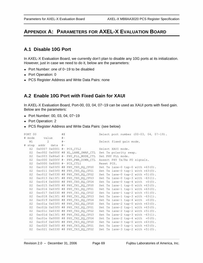
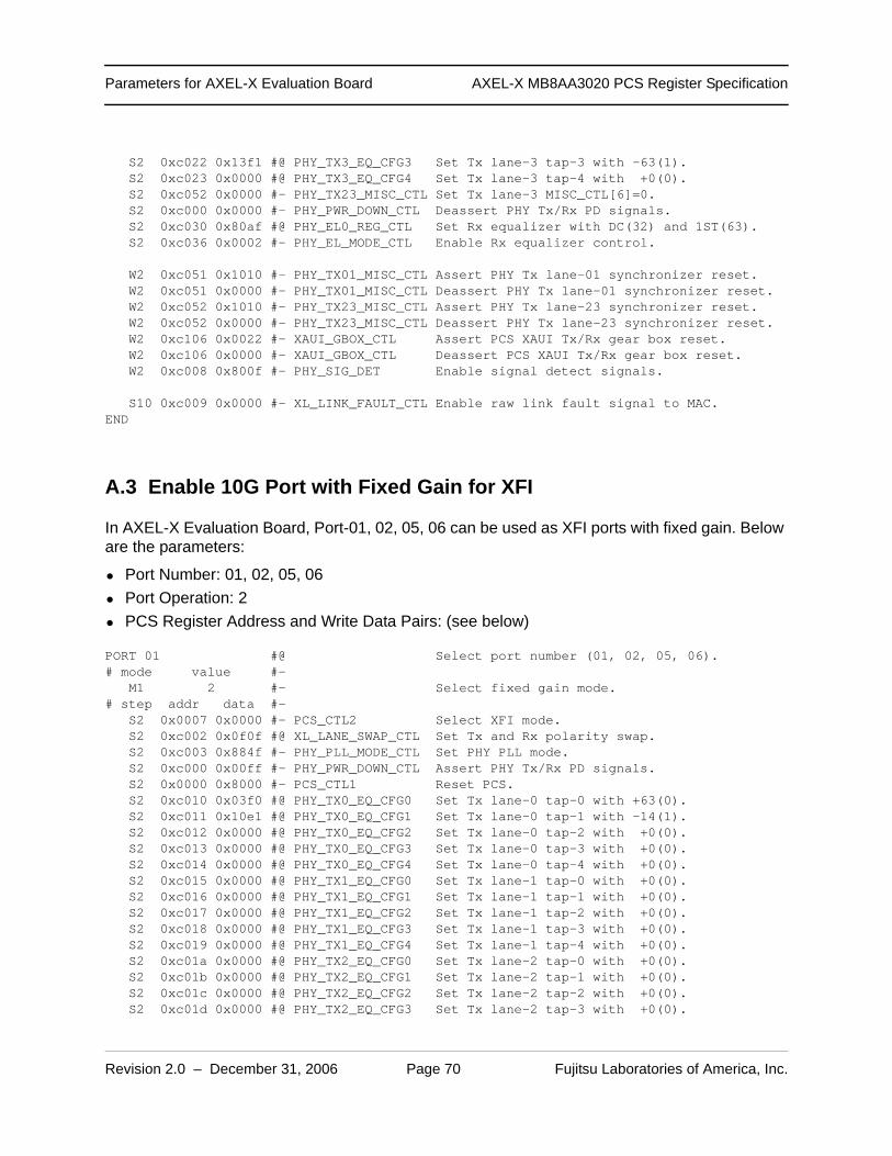
AXEL-X has twenty 10G ports (Port-0 ~ 19), and each can be configured as 10GBASE-X (XAUI, CX4) mode or 10GBASE-R (XFI) mode individually.
This document describes how to configure AXEL-X 10G ports and provides the following specifi-cation and/or information for an actual application of AXEL-X chip:
• AXEL-X initialization flow overview• 10G port PCS-PHY configuration flows• How to choose PCS-PHY Tx parameters• How to choose PCS-PHY Rx parameters• PCS register specification
1.2 AXEL-X Initialization Flow
After powering on AXEL-X or applying the hardware reset, AXEL-X chip loads the on-chip code from EEPROM and the micro-engine starts executing the on-chip code by itself. The on-chip code configures all twenty 10G PCS-PHY ports as a part of the AXEL-X initialization.
Figure 1 shows the AXEL-X initialization flow.
The following is the brief explanation of each step in the AXEL-X initialization flow:
• Step-1: Power up AXEL-X and XI_POWER_GOOD signal of AXEL-X input pin goes high when the AXEL-X power voltage reaches a certain level. Refer to “AXEL-X MB8AA3020 Chip Specification” document for details.
• Step-2: Apply hardware reset. XI_RESET_PLL_N and XI_RESET_N signals of AXEL-X input pins go high at the specific sequence and timing. Refer to “AXEL-X Chip Specification” docu-ment for details.
• Step-3: The on-chip code is loaded from EEPROM through I2C bus and the micro engine starts executing the code by itself. Refer to “AXEL-X MB8AA3020 Chip Specification” docu-ment for details.
• Step-4: Initialize switch core and GbE ports (port-21 and 23) by the on-chip code. Refer to “AXEL-X MB8AA3020 On-Chip Code Specification” document for details.
• Step-5: Disable 10G port. This is one of three possible configurations of a 10G port. The selection is made port by port. This step is done as a part of the AXEL-X initialization by the on-chip code originally stored in EEPROM. This step is described in details later in this docu-ment.
Page 6
Revision 2.0 – December 31, 2006 Page 6 Fujitsu Laboratories of America, Inc.
Overview AXEL-X MB8AA3020 PCS Register Specification
• Step-6: Enable 10G port with Fixed Gain Mode. This is one of three possible configurations of a 10G port. The selection is made port by port. This step is done as a part of the AXEL-X ini-tialization by the on-chip code originally stored in EEPROM. This step is described in details later in this document.
• Step-7: Enable 10G port with Adaptive Mode. This is one of three possible configurations of a 10G port. The selection is made port by port. This step is done as a part of the AXEL-X initial-ization by the on-chip code originally stored in EEPROM. This step is described in details later in this document.
Figure 1. AXEL-X Initialization Flow
S1
S2
S3
S4 Initialize Switch Core
Disable 10G Port S6 S7
Hardware Reset
Software Reset
S5 Enable 10G Port Enable 10G Portwith Adaptive Mode
Power up AXEL-X
Apply HW Reset
Load On-Chip Code from
Each 10G Port (Port by Port Control)
and GbE Ports
EEPROM and Start ME
with Fixed Gain Mode
Page 7
10G Port Configuration Flows AXEL-X MB8AA3020 PCS Register Specification
Revision 2.0 – December 31, 2006 Page 7 Fujitsu Laboratories of America, Inc.
CHAPTER 2: 10G PORT CONFIGURATION FLOWS
2.1 Configuration Flows
The following three sub chapters describe the step-5, 6,and 7 flows in Figure 1 in Chapter 1.
Each step consists of sub steps which are described in a table. Each table shows the register access sequence. In the register access sequences, the register write values are written in actual values in hex or parameters whose name starts with “$” sign.
In the case of hex values, the write values are fixed. In the case of parameters, the write values differ depending on each application case and are stored in EEPROM as a set of data for the AXEL-X initialization.
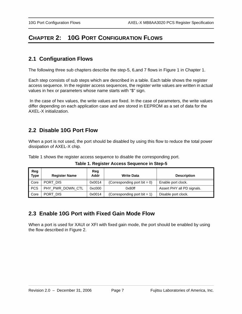
2.2 Disable 10G Port Flow
When a port is not used, the port should be disabled by using this flow to reduce the total power dissipation of AXEL-X chip.
Table 1 shows the register access sequence to disable the corresponding port.
2.3 Enable 10G Port with Fixed Gain Mode Flow
When a port is used for XAUI or XFI with fixed gain mode, the port should be enabled by using the flow described in Figure 2.
Table 1. Register Access Sequence in Step-5Reg Type Register Name
Reg Addr Write Data Description
Core PORT_DIS 0x0014 (Corresponding port bit = 0) Enable port clock.
PCS PHY_PWR_DOWN_CTL 0xc000 0x80ff Assert PHY all PD signals.
Core PORT_DIS 0x0014 (Corresponding port bit = 1) Disable port clock.
Page 8
Revision 2.0 – December 31, 2006 Page 8 Fujitsu Laboratories of America, Inc.
10G Port Configuration Flows AXEL-X MB8AA3020 PCS Register Specification
Table 2 shows the register access sequence in Step-6.1.Table 2. Register Access Sequence in Step-6.1
Reg Type Register Name
Reg Addr Write Data Description
Core PORT_DIS 0x0014 (Corresponding port bit = 0) Enable port clock.
PCS PCS_CTL2 0x0007 0x0001 (for XAUI)0x0000 (for XFI)
Select XAUI or XFI mode.
Figure 2. Enable 10G Port with Fixed Gain Mode
S6.6
S6
S6.1
S6.5 Enable Raw Link FaultStatus Signal to MAC
S6
S6.4 Wait for 50mS
Start
Set PCS-PHY
End
Enable MAC Tx and Rx
with Fixed Gain Mode
S6.2 Wait for 1mS
S6.3 Reset PHY-PCS Gear Boxes
(S2)
(W1)
(W2)
(S6)
(S10)
(S11)
Page 9
Revision 2.0 – December 31, 2006 Page 9 Fujitsu Laboratories of America, Inc.
10G Port Configuration Flows AXEL-X MB8AA3020 PCS Register Specification
PCS XL_LANE_SWAP_CTL 0xc002 $XL_LANE_SWAP_CTL Set Tx/Rx lane and polarity swap.
PCS PHY_PLL_MODE_CTL 0xc003 $PHY_PLL_MODE_CTL Set PHY PLL mode.
PCS PHY_PWR_DOWN_CTL 0xc000 0x00ff Assert PHY Tx/Rx PD signals.Deassert PHY USR PD signal if it has been asserted.
PCS PCS_CTL1 0x0000 0x8000 Reset PCS.
PCS PHY_TX0_EQ_CFG0 0xc010 $PHY_TX0_EQ_CFG0 Set Tx lane-0 equalizer tap-0.
PCS PHY_TX0_EQ_CFG1 0xc011 $PHY_TX0_EQ_CFG1 Set Tx lane-0 equalizer tap-1.
PCS PHY_TX0_EQ_CFG2 0xc012 $PHY_TX0_EQ_CFG2 Set Tx lane-0 equalizer tap-2.
PCS PHY_TX0_EQ_CFG3 0xc013 $PHY_TX0_EQ_CFG3 Set Tx lane-0 equalizer tap-3.
PCS PHY_TX0_EQ_CFG4 0xc014 $PHY_TX0_EQ_CFG4 Set Tx lane-0 equalizer tap-4.
PCS PHY_TX1_EQ_CFG0 0xc015 $PHY_TX1_EQ_CFG0 Set Tx lane-1 equalizer tap-0.
PCS PHY_TX1_EQ_CFG1 0xc016 $PHY_TX1_EQ_CFG1 Set Tx lane-1 equalizer tap-1.
PCS PHY_TX1_EQ_CFG2 0xc017 $PHY_TX1_EQ_CFG2 Set Tx lane-1 equalizer tap-2.
PCS PHY_TX1_EQ_CFG3 0xc018 $PHY_TX1_EQ_CFG3 Set Tx lane-1 equalizer tap-3.
PCS PHY_TX1_EQ_CFG4 0xc019 $PHY_TX1_EQ_CFG4 Set Tx lane-1 equalizer tap-4.
PCS PHY_TX2_EQ_CFG0 0xc01a $PHY_TX2_EQ_CFG0 Set Tx lane-2 equalizer tap-0.
PCS PHY_TX2_EQ_CFG1 0xc01b $PHY_TX2_EQ_CFG1 Set Tx lane-2 equalizer tap-1.
PCS PHY_TX2_EQ_CFG2 0xc01c $PHY_TX2_EQ_CFG2 Set Tx lane-2 equalizer tap-2.
PCS PHY_TX2_EQ_CFG3 0xc01d $PHY_TX2_EQ_CFG3 Set Tx lane-2 equalizer tap-3.
PCS PHY_TX2_EQ_CFG4 0xc01e $PHY_TX2_EQ_CFG4 Set Tx lane-2 equalizer tap-4.
PCS PHY_TX3_EQ_CFG0 0xc01f $PHY_TX3_EQ_CFG0 Set Tx lane-3 equalizer tap-0.
PCS PHY_TX3_EQ_CFG1 0xc020 $PHY_TX3_EQ_CFG1 Set Tx lane-3 equalizer tap-1.
PCS PHY_TX3_EQ_CFG2 0xc021 $PHY_TX3_EQ_CFG2 Set Tx lane-3 equalizer tap-2.
PCS PHY_TX3_EQ_CFG3 0xc022 $PHY_TX3_EQ_CFG3 Set Tx lane-3 equalizer tap-3.
PCS PHY_TX3_EQ_CFG4 0xc023 $PHY_TX3_EQ_CFG4 Set Tx lane-3 equalizer tap-4.
PCS PHY_TX23_MISC_CTL 0xc052 0x0000 (XAUI)0x4000 (XFI)
Set Tx lane-3 misc control bit-6.
PCS PHY_PWR_DOWN_CTL 0xc000 0x0000 (XAUI)0x00e6 (XFI)
Deassert PHY Tx/Rx PD signals.
PCS PHY_EL0_REG_CTL 0xc030 $PHY_EL0_REG_CTL Set Rx equalizer parameters.
PCS PHY_EL_MODE_CTL 0xc036 0x0002 Enable Rx equalizer controls.
Table 2. Register Access Sequence in Step-6.1Reg Type Register Name
Reg Addr Write Data Description
Page 10
Revision 2.0 – December 31, 2006 Page 10 Fujitsu Laboratories of America, Inc.
10G Port Configuration Flows AXEL-X MB8AA3020 PCS Register Specification
Table 3 shows the register access sequence in Step-6.3.
Table 4 shows the register access sequence in Step-6.5.
Table 3. Register Access Sequence in Step-6.3Reg Type Register Name
Reg Addr Write Data Description
PCS PHY_TX01_MISC_CTL 0xc051 0x1010 Assert PHY Tx lane-01 synchro-nizer reset.
PCS PHY_TX01_MISC_CTL 0xc051 0x0000 Deassert PHY Tx lane-01 syn-chronizer reset.
PCS PHY_TX23_MISC_CTL 0xc052 0x1010 (XAUI)0x5010 (XFI)
Assert PHY Tx lane-23 synchro-nizer reset.
PCS PHY_TX23_MISC_CTL 0xc052 0x0000 (XAUI)0x4000 (XFI)
Deassert PHY Tx lane-23 syn-chronizer reset.
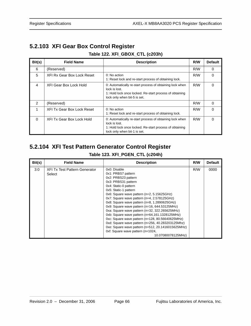
PCS XAUI_GBOX_CTL (XAUI)XFI_GBOX_CTL (XFI)
0xc106 (XAUI)0xc203 (XFI)
0x0022 Assert PCS XAUI Tx and Rx gear box reset. (XAUI)Assert PCS XFI Tx and Rx gear box reset. (XFI)
PCS XAUI_GBOX_CTL (XAUI)XFI_GBOX_CTL (XFI)
0xc106 (XAUI)0xc203 (XFI)
0x0000 Deassert PCS XAUI Tx and Rx gear box reset. (XAUI)Deassert PCS XFI Tx and Rx gear box reset. (XFI)
PCS PHY_SIG_DET 0xc008 0x800f Enable signal detect signals.
Table 4. Register Access Sequence in Step-6.5Reg Type Register Name
Reg Addr Write Data Description
PCS XL_LINK_FAULT_CTL 0xc009 0x0000 Enable raw link fault status signal to MAC.
Page 11
Revision 2.0 – December 31, 2006 Page 11 Fujitsu Laboratories of America, Inc.
10G Port Configuration Flows AXEL-X MB8AA3020 PCS Register Specification
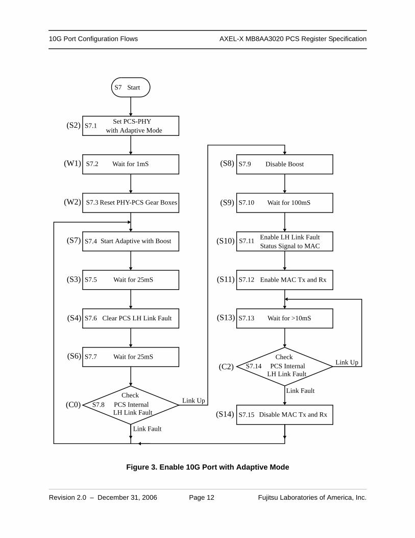
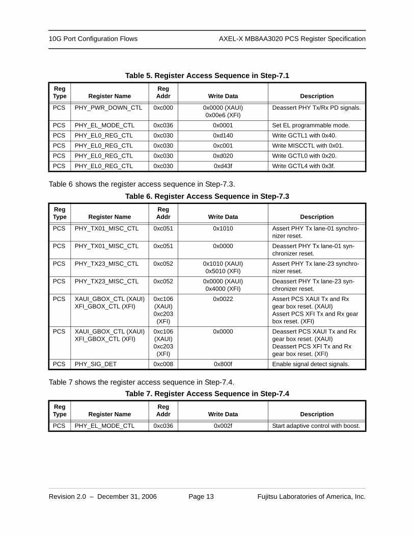
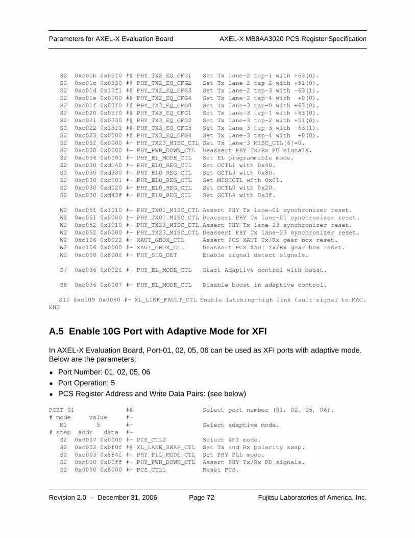
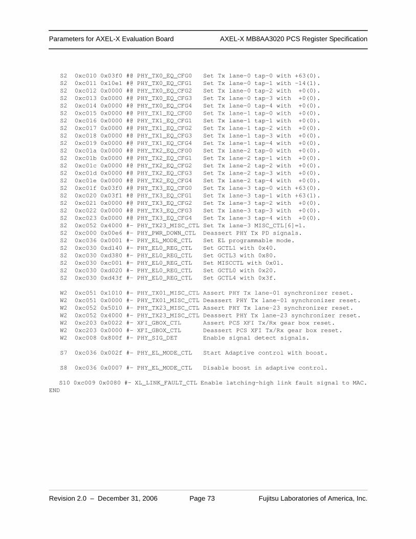
2.4 Enable 10G Port with Adaptive Mode Flow
When a port is used for XAUI or XFI with adaptive mode, the port should be enabled by using the flow described in Figure 3.
Table 5 shows the register access sequence in Step-7.1.Table 5. Register Access Sequence in Step-7.1
Reg Type Register Name
Reg Addr Write Data Description
Core PORT_DIS 0x0014 (Corresponding port bit = 0) Enable port clock.
PCS PCS_CTL2 0x0007 0x0001 (for XAUI)0x0000 (for XFI)
Select XAUI or XFI mode.
PCS XL_LANE_SWAP_CTL 0xc002 $XL_LANE_SWAP_CTL Set Tx/Rx lane and polarity swap.
PCS PHY_PLL_MODE_CTL 0xc003 $PHY_PLL_MODE_CTL Set PHY PLL mode.
PCS PHY_PWR_DOWN_CTL 0xc000 0x00ff Assert PHY Tx/Rx PD signals.Deassert PHY USR PD signal if it has been asserted.
PCS PCS_CTRL1 0x0000 0x8000 Reset PCS.
PCS PHY_TX0_EQ_CFG0 0xc010 $PHY_TX0_EQ_CFG0 Set Tx lane-0 equalizer tap-0.
PCS PHY_TX0_EQ_CFG1 0xc011 $PHY_TX0_EQ_CFG1 Set Tx lane-0 equalizer tap-1.
PCS PHY_TX0_EQ_CFG2 0xc012 $PHY_TX0_EQ_CFG2 Set Tx lane-0 equalizer tap-2.
PCS PHY_TX0_EQ_CFG3 0xc013 $PHY_TX0_EQ_CFG3 Set Tx lane-0 equalizer tap-3.
PCS PHY_TX0_EQ_CFG4 0xc014 $PHY_TX0_EQ_CFG4 Set Tx lane-0 equalizer tap-4.
PCS PHY_TX1_EQ_CFG0 0xc015 $PHY_TX1_EQ_CFG0 Set Tx lane-1 equalizer tap-0.
PCS PHY_TX1_EQ_CFG1 0xc016 $PHY_TX1_EQ_CFG1 Set Tx lane-1 equalizer tap-1.
PCS PHY_TX1_EQ_CFG2 0xc017 $PHY_TX1_EQ_CFG2 Set Tx lane-1 equalizer tap-2.
PCS PHY_TX1_EQ_CFG3 0xc018 $PHY_TX1_EQ_CFG3 Set Tx lane-1 equalizer tap-3.
PCS PHY_TX1_EQ_CFG4 0xc019 $PHY_TX1_EQ_CFG4 Set Tx lane-1 equalizer tap-4.
PCS PHY_TX2_EQ_CFG0 0xc01a $PHY_TX2_EQ_CFG0 Set Tx lane-2 equalizer tap-0.
PCS PHY_TX2_EQ_CFG1 0xc01b $PHY_TX2_EQ_CFG1 Set Tx lane-2 equalizer tap-1.
PCS PHY_TX2_EQ_CFG2 0xc01c $PHY_TX2_EQ_CFG2 Set Tx lane-2 equalizer tap-2.
PCS PHY_TX2_EQ_CFG3 0xc01d $PHY_TX2_EQ_CFG3 Set Tx lane-2 equalizer tap-3.
PCS PHY_TX2_EQ_CFG4 0xc01e $PHY_TX2_EQ_CFG4 Set Tx lane-2 equalizer tap-4.
PCS PHY_TX3_EQ_CFG0 0xc01f $PHY_TX3_EQ_CFG0 Set Tx lane-3 equalizer tap-0.
PCS PHY_TX3_EQ_CFG1 0xc020 $PHY_TX3_EQ_CFG1 Set Tx lane-3 equalizer tap-1.
PCS PHY_TX3_EQ_CFG2 0xc021 $PHY_TX3_EQ_CFG2 Set Tx lane-3 equalizer tap-2.
PCS PHY_TX3_EQ_CFG3 0xc022 $PHY_TX3_EQ_CFG3 Set Tx lane-3 equalizer tap-3.
PCS PHY_TX3_EQ_CFG4 0xc023 $PHY_TX3_EQ_CFG4 Set Tx lane-3 equalizer tap-4.
PCS PHY_TX23_MISC_CTL 0xc052 0x0000 (XAUI)0x4000 (XFI)
Set Tx lane-3 misc control bit-6.
Page 12
Revision 2.0 – December 31, 2006 Page 12 Fujitsu Laboratories of America, Inc.
10G Port Configuration Flows AXEL-X MB8AA3020 PCS Register Specification
Figure 3. Enable 10G Port with Adaptive Mode
S7.12
S7
S7.4
CheckPCS InternalLH Link Fault
S7.8
Link Fault
Link Up
S7.11 Enable LH Link FaultStatus Signal to MAC
CheckPCS Internal
LH Link FaultS7.14
S7.15
Link Up
Link Fault
Start
Start Adaptive with Boost
Enable MAC Tx and Rx
Disable MAC Tx and Rx
S7.5 Wait for 25mS
S7.13 Wait for >10mS
S7.1 Set PCS-PHYwith Adaptive Mode
S7.6 Clear PCS LH Link Fault
S7.7 Wait for 25mS
S7.9 Disable Boost
S7.10 Wait for 100mS
S7.2 Wait for 1mS
S7.3 Reset PHY-PCS Gear Boxes
(S2)
(W1)
(W2)
(S7)
(S3)
(S4)
(S6)
(C0)
(S8)
(S9)
(S10)
(S11)
(S13)
(C2)
(S14)
Page 13
Revision 2.0 – December 31, 2006 Page 13 Fujitsu Laboratories of America, Inc.
10G Port Configuration Flows AXEL-X MB8AA3020 PCS Register Specification
Table 6 shows the register access sequence in Step-7.3.
Table 7 shows the register access sequence in Step-7.4.
PCS PHY_PWR_DOWN_CTL 0xc000 0x0000 (XAUI)0x00e6 (XFI)
Deassert PHY Tx/Rx PD signals.
PCS PHY_EL_MODE_CTL 0xc036 0x0001 Set EL programmable mode.
PCS PHY_EL0_REG_CTL 0xc030 0xd140 Write GCTL1 with 0x40.
PCS PHY_EL0_REG_CTL 0xc030 0xc001 Write MISCCTL with 0x01.
PCS PHY_EL0_REG_CTL 0xc030 0xd020 Write GCTL0 with 0x20.
PCS PHY_EL0_REG_CTL 0xc030 0xd43f Write GCTL4 with 0x3f.
Table 6. Register Access Sequence in Step-7.3Reg Type Register Name
Reg Addr Write Data Description
PCS PHY_TX01_MISC_CTL 0xc051 0x1010 Assert PHY Tx lane-01 synchro-nizer reset.
PCS PHY_TX01_MISC_CTL 0xc051 0x0000 Deassert PHY Tx lane-01 syn-chronizer reset.
PCS PHY_TX23_MISC_CTL 0xc052 0x1010 (XAUI)0x5010 (XFI)
Assert PHY Tx lane-23 synchro-nizer reset.
PCS PHY_TX23_MISC_CTL 0xc052 0x0000 (XAUI)0x4000 (XFI)
Deassert PHY Tx lane-23 syn-chronizer reset.
PCS XAUI_GBOX_CTL (XAUI)XFI_GBOX_CTL (XFI)
0xc106 (XAUI)0xc203 (XFI)
0x0022 Assert PCS XAUI Tx and Rx gear box reset. (XAUI)Assert PCS XFI Tx and Rx gear box reset. (XFI)
PCS XAUI_GBOX_CTL (XAUI)XFI_GBOX_CTL (XFI)
0xc106 (XAUI)0xc203 (XFI)
0x0000 Deassert PCS XAUI Tx and Rx gear box reset. (XAUI)Deassert PCS XFI Tx and Rx gear box reset. (XFI)
PCS PHY_SIG_DET 0xc008 0x800f Enable signal detect signals.
Table 7. Register Access Sequence in Step-7.4Reg Type Register Name
Reg Addr Write Data Description
PCS PHY_EL_MODE_CTL 0xc036 0x002f Start adaptive control with boost.
Table 5. Register Access Sequence in Step-7.1Reg Type Register Name
Reg Addr Write Data Description
Page 14
Revision 2.0 – December 31, 2006 Page 14 Fujitsu Laboratories of America, Inc.
10G Port Configuration Flows AXEL-X MB8AA3020 PCS Register Specification
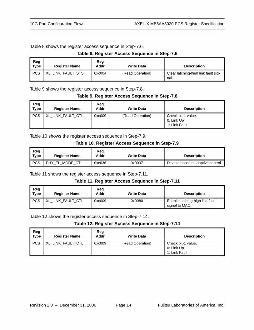
Table 8 shows the register access sequence in Step-7.6.
Table 9 shows the register access sequence in Step-7.8.
Table 10 shows the register access sequence in Step-7.9.
Table 11 shows the register access sequence in Step-7.11.
Table 12 shows the register access sequence in Step-7.14.
Table 8. Register Access Sequence in Step-7.6Reg Type Register Name
Reg Addr Write Data Description
PCS XL_LINK_FAULT_STS 0xc00a (Read Operation) Clear latching-high link fault sig-nal.
Table 9. Register Access Sequence in Step-7.8Reg Type Register Name
Reg Addr Write Data Description
PCS XL_LINK_FAULT_CTL 0xc009 (Read Operation) Check bit-1 value.0: Link Up1: Link Fault
Table 10. Register Access Sequence in Step-7.9Reg Type Register Name
Reg Addr Write Data Description
PCS PHY_EL_MODE_CTL 0xc036 0x0007 Disable boost in adaptive control.
Table 11. Register Access Sequence in Step-7.11Reg Type Register Name
Reg Addr Write Data Description
PCS XL_LINK_FAULT_CTL 0xc009 0x0080 Enable latching-high link fault signal to MAC.
Table 12. Register Access Sequence in Step-7.14Reg Type Register Name
Reg Addr Write Data Description
PCS XL_LINK_FAULT_CTL 0xc009 (Read Operation) Check bit-1 value.0: Link Up1: Link Fault
Page 15
Tx Parameters AXEL-X MB8AA3020 PCS Register Specification
Revision 2.0 – December 31, 2006 Page 15 Fujitsu Laboratories of America, Inc.
CHAPTER 3: TX PARAMETERS
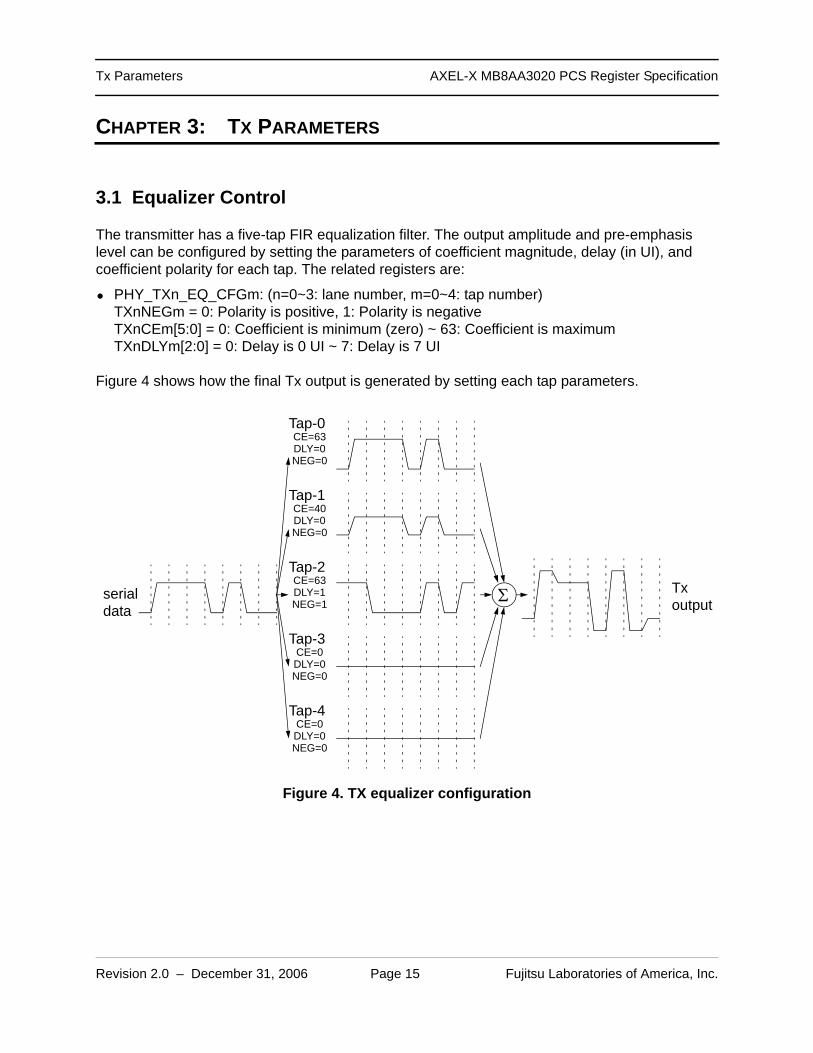
3.1 Equalizer Control
The transmitter has a five-tap FIR equalization filter. The output amplitude and pre-emphasis level can be configured by setting the parameters of coefficient magnitude, delay (in UI), and coefficient polarity for each tap. The related registers are:
• PHY_TXn_EQ_CFGm: (n=0~3: lane number, m=0~4: tap number)TXnNEGm = 0: Polarity is positive, 1: Polarity is negativeTXnCEm[5:0] = 0: Coefficient is minimum (zero) ~ 63: Coefficient is maximumTXnDLYm[2:0] = 0: Delay is 0 UI ~ 7: Delay is 7 UI
Figure 4 shows how the final Tx output is generated by setting each tap parameters.
Figure 4. TX equalizer configuration
serialdata
Tap-0
Tap-1
Tap-2
Tap-3
Tap-4
CE=63DLY=0NEG=0
CE=40DLY=0NEG=0
CE=63DLY=1NEG=1
CE=0DLY=0NEG=0
CE=0DLY=0NEG=0
Tx outputΣ
Page 16
Revision 2.0 – December 31, 2006 Page 16 Fujitsu Laboratories of America, Inc.
Tx Parameters AXEL-X MB8AA3020 PCS Register Specification
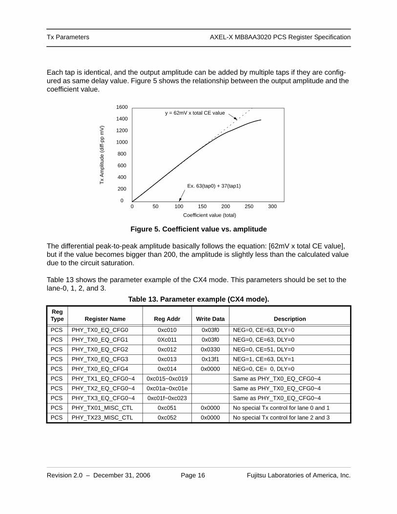
Each tap is identical, and the output amplitude can be added by multiple taps if they are config-ured as same delay value. Figure 5 shows the relationship between the output amplitude and the coefficient value.
The differential peak-to-peak amplitude basically follows the equation: [62mV x total CE value], but if the value becomes bigger than 200, the amplitude is slightly less than the calculated value due to the circuit saturation.
Table 13 shows the parameter example of the CX4 mode. This parameters should be set to the lane-0, 1, 2, and 3.
Figure 5. Coefficient value vs. amplitude
Table 13. Parameter example (CX4 mode).Reg Type Register Name Reg Addr Write Data Description
PCS PHY_TX0_EQ_CFG0 0xc010 0x03f0 NEG=0, CE=63, DLY=0
PCS PHY_TX0_EQ_CFG1 0Xc011 0x03f0 NEG=0, CE=63, DLY=0
PCS PHY_TX0_EQ_CFG2 0xc012 0x0330 NEG=0, CE=51, DLY=0
PCS PHY_TX0_EQ_CFG3 0xc013 0x13f1 NEG=1, CE=63, DLY=1
PCS PHY_TX0_EQ_CFG4 0xc014 0x0000 NEG=0, CE= 0, DLY=0
PCS PHY_TX1_EQ_CFG0~4 0xc015~0xc019 Same as PHY_TX0_EQ_CFG0~4
PCS PHY_TX2_EQ_CFG0~4 0xc01a~0xc01e Same as PHY_TX0_EQ_CFG0~4
PCS PHY_TX3_EQ_CFG0~4 0xc01f~0xc023 Same as PHY_TX0_EQ_CFG0~4
PCS PHY_TX01_MISC_CTL 0xc051 0x0000 No special Tx control for lane 0 and 1
PCS PHY_TX23_MISC_CTL 0xc052 0x0000 No special Tx control for lane 2 and 3
Tx A
mpl
itude
(diff
-pp
mV
)
Coefficient value (total)
1600
1400
1200
1000
800
600
400
200
00 50 100 150 200 250 300
y = 62mV x total CE value
Ex. 63(tap0) + 37(tap1)
Page 17
Revision 2.0 – December 31, 2006 Page 17 Fujitsu Laboratories of America, Inc.
Tx Parameters AXEL-X MB8AA3020 PCS Register Specification
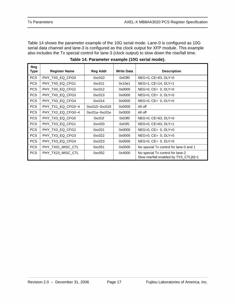
Table 14 shows the parameter example of the 10G serial mode. Lane-0 is configured as 10G serial data channel and lane-3 is configured as the clock output for XFP module. This example also includes the Tx special control for lane-3 (clock output) to slow down the rise/fall time.
Table 14. Parameter example (10G serial mode).Reg Type Register Name Reg Addr Write Data Description
PCS PHY_TX0_EQ_CFG0 0xc010 0x03f0 NEG=0, CE=63, DLY=0
PCS PHY_TX0_EQ_CFG1 0xc011 0x10e1 NEG=1, CE=14, DLY=1
PCS PHY_TX0_EQ_CFG2 0xc012 0x0000 NEG=0, CE= 0, DLY=0
PCS PHY_TX0_EQ_CFG3 0xc013 0x0000 NEG=0, CE= 0, DLY=0
PCS PHY_TX0_EQ_CFG4 0xc014 0x0000 NEG=0, CE= 0, DLY=0
PCS PHY_TX1_EQ_CFG0~4 0xc015~0xc019 0x0000 All off
PCS PHY_TX2_EQ_CFG0~4 0xc01a~0xc01e 0x0000 All off
PCS PHY_TX3_EQ_CFG0 0xc01f 0x03f0 NEG=0, CE=63, DLY=0
PCS PHY_TX3_EQ_CFG1 0xc020 0x03f1 NEG=0, CE=63, DLY=1
PCS PHY_TX3_EQ_CFG2 0xc021 0x0000 NEG=0, CE= 0, DLY=0
PCS PHY_TX3_EQ_CFG3 0xc022 0x0000 NEG=0, CE= 0, DLY=0
PCS PHY_TX3_EQ_CFG4 0xc023 0x0000 NEG=0, CE= 0, DLY=0
PCS PHY_TX01_MISC_CTL 0xc051 0x0000 No special Tx control for lane-0 and 1
PCS PHY_TX23_MISC_CTL 0xc052 0x4000 No special Tx control for lane-2.Slow rise/fall enabled by TX3_CTL[6]=1
Page 18
Revision 2.0 – December 31, 2006 Page 18 Fujitsu Laboratories of America, Inc.
Tx Parameters AXEL-X MB8AA3020 PCS Register Specification
3.2 Tx Synchronizer Initialization
There is an data synchronizer inside the Tx macro and it has to be initialized whenever the Tx channel comes out of the power-down state. Figure 6 shows how to initialize the Tx macro syn-chronizer.
Figure 6. TX synchronizer initialization
User PD
Tx channel PD
Macro PLL start
Tx start
>= 0 us
>= 10 usTx synchronizer reset.Write the registers in the following order:PHY_TX01_MISC_CTL(0xc051) <= 0x0101PHY_TX01_MISC_CTL(0xc051) <= 0x0000PHY_TX23_MISC_CTL(0xc052) <= 0x0101PHY_TX23_MISC_CTL(0xc052) <= 0x0000
Page 19
Rx Parameters AXEL-X MB8AA3020 PCS Register Specification
Revision 2.0 – December 31, 2006 Page 19 Fujitsu Laboratories of America, Inc.
CHAPTER 4: RX PARAMETERS
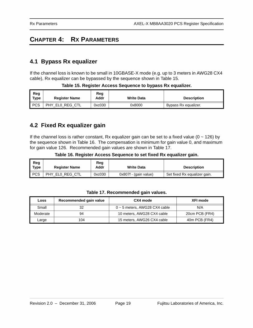
4.1 Bypass Rx equalizer
If the channel loss is known to be small in 10GBASE-X mode (e.g. up to 3 meters in AWG28 CX4 cable), Rx equalizer can be bypassed by the sequence shown in Table 15.
4.2 Fixed Rx equalizer gain
If the channel loss is rather constant, Rx equalizer gain can be set to a fixed value (0 ~ 126) by the sequence shown in Table 16. The compensation is minimum for gain value 0, and maximum for gain value 126. Recommended gain values are shown in Table 17.
Table 15. Register Access Sequence to bypass Rx equalizer.Reg Type Register Name
Reg Addr Write Data Description
PCS PHY_EL0_REG_CTL 0xc030 0x8000 Bypass Rx equalizer.
Table 16. Register Access Sequence to set fixed Rx equalizer gain.Reg Type Register Name
Reg Addr Write Data Description
PCS PHY_EL0_REG_CTL 0xc030 0x807f - (gain value) Set fixed Rx equalizer gain.
Table 17. Recommended gain values.Loss Recommended gain value CX4 mode XFI mode
Small 32 0 ~ 5 meters, AWG28 CX4 cable N/A
Moderate 94 10 meters, AWG28 CX4 cable 20cm PCB (FR4)
Large 104 15 meters, AWG26 CX4 cable 40m PCB (FR4)
Page 20
Revision 2.0 – December 31, 2006 Page 20 Fujitsu Laboratories of America, Inc.
Rx Parameters AXEL-X MB8AA3020 PCS Register Specification
4.3 Adaptive Rx equalizer gain
If the channel loss is unknown, Rx equalizer gain can be adapted to the channel loss by the sequence shown in Table 18. This sequence needs to be restarted after receiving the incoming signal, which can be checked by the link fault status.
Table 18. Register Access Sequence to set adaptive Rx equalizer gain.Reg Type Register Name
Reg Addr Write Data Description
PCS PHY_EL_MODE_CTL 0xc036 0x0001 Set EL programmable mode.
PCS PHY_EL0_REG_CTL 0xc030 0xd140 Write GCTL1 with 0x40.
PCS PHY_EL0_REG_CTL 0xc030 0xd380 Write GCTL3 with 0x80.
PCS PHY_EL0_REG_CTL 0xc030 0xc001 Write MISCCTL with 0x01.
PCS PHY_EL0_REG_CTL 0xc030 0xd020 Write GCTL0 with 0x20.
PCS PHY_EL0_REG_CTL 0xc030 0xd43f Write GCTL4 with 0x3f.
PCS PHY_EL_MODE_CTL 0xc036 0x002f Restart adaptive cont. w/ boost.
Wait for more than 25ms Do coarse adjustment.
PCS PHY_EL_MODE_CTL 0xc036 0x0007 Set adaptive control w/o boost.
Wait for more than 100ms Do fine adjustment.
Page 21
Register Specifications AXEL-X MB8AA3020 PCS Register Specification
Revision 2.0 – December 31, 2006 Page 21 Fujitsu Laboratories of America, Inc.
CHAPTER 5: REGISTER SPECIFICATIONS
5.1 Overview
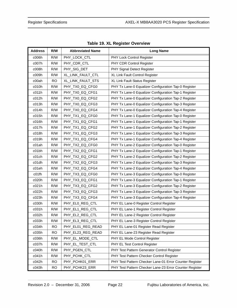
Table 19 shows the XL register overview.Table 19. XL Register Overview
Address R/W Abbreviated Name Long Name
0000h R/W PCS_CTL1 PCS Control 1 Register
0001h RO PCS_STS1 PCS Status 1 Register
0002h RO PCS_DEV_ID0 PCS Device Identifier 0 Register
0003h RO PCS_DEV_ID1 PCS Device Identifier 1 Register
0004h RO PCS_SPEED PCS Speed Ability Register
0005h RO PCS_DEV_IN_PKG0 PCS Device In Package 0 Register
0006h RO PCS_DEV_IN_PKG1 PCS Device In Package 1 Register
0007h RW PCS_CTL2 PCS Control 2 Register
0008h RO PCS_STS2 PCS Status 2 Register
000eh RO PCS_PKG_ID0 PCS Package Identifier 0 Register
000fh RO PCS_PKG_ID1 PCS Package Identifier 1 Register
0018h RO PCS_XAUI_STS PCS XAUI Status Register
0019h R/W PCS_XAUI_TEST_CTL PCS XAUI Test Control Register
0020h RO PCS_XFI_STS1 PCS XFI Status 1 Register
0021h RO PCS_XFI_STS2 PCS XFI Status 2 Register
0022h R/W PCS_XFI_TEST_SEEDA0 PCS XFI Test Pattern Seed A0 Register
0023h R/W PCS_XFI_TEST_SEEDA1 PCS XFI Test Pattern Seed A1 Register
0024h R/W PCS_XFI_TEST_SEEDA2 PCS XFI Test Pattern Seed A2 Register
0025h R/W PCS_XFI_TEST_SEEDA3 PCS XFI Test Pattern Seed A3 Register
0026h R/W PCS_XFI_TEST_SEEDB0 PCS XFI Test Pattern Seed B0 Register
0027h R/W PCS_XFI_TEST_SEEDB1 PCS XFI Test Pattern Seed B1 Register
0028h R/W PCS_XFI_TEST_SEEDB2 PCS XFI Test Pattern Seed B2 Register
0029h R/W PCS_XFI_TEST_SEEDB3 PCS XFI Test Pattern Seed B3 Register
002ah R/W PCS_XFI_TEST_CTL PCS XFI Test Pattern Control Register
002bh RO PCS_XFI_TEST_ERR PCS XFI Test Pattern Error Counter Register
c000h R/W PHY_PWR_DOWN_CTL PHY Power Down Control Register
c001h R/W PHY_CURR_BIAS_CTL PHY Current Bias Control Register
c002h R/W XL_LANE_SWAP_CTL XL Lane Polarity Swap Control Register
c003h R/W PHY_PLL_MODE_CTL PHY PLL Mode Control Register
c004h R/W PHY_TX_MODE_CTL PHY Tx Mode Control Register
c005h R/W PHY_RX_MODE_CTL PHY Rx Mode Control Register
Page 22
Revision 2.0 – December 31, 2006 Page 22 Fujitsu Laboratories of America, Inc.
Register Specifications AXEL-X MB8AA3020 PCS Register Specification
c006h R/W PHY_LOCK_CTL PHY Lock Control Register
c007h R/W PHY_CDR_CTL PHY CDR Control Register
c008h R/W PHY_SIG_DET PHY Signal Detect Register
c009h R/W XL_LINK_FAULT_CTL XL Link Fault Control Register
c00ah RO XL_LINK_FAULT_STS XL Link Fault Status Register
c010h R/W PHY_TX0_EQ_CFG0 PHY Tx Lane-0 Equalizer Configuration Tap-0 Register
c011h R/W PHY_TX0_EQ_CFG1 PHY Tx Lane-0 Equalizer Configuration Tap-1 Register
c012h R/W PHY_TX0_EQ_CFG2 PHY Tx Lane-0 Equalizer Configuration Tap-2 Register
c013h R/W PHY_TX0_EQ_CFG3 PHY Tx Lane-0 Equalizer Configuration Tap-3 Register
c014h R/W PHY_TX0_EQ_CFG4 PHY Tx Lane-0 Equalizer Configuration Tap-4 Register
c015h R/W PHY_TX1_EQ_CFG0 PHY Tx Lane-1 Equalizer Configuration Tap-0 Register
c016h R/W PHY_TX1_EQ_CFG1 PHY Tx Lane-1 Equalizer Configuration Tap-1 Register
c017h R/W PHY_TX1_EQ_CFG2 PHY Tx Lane-1 Equalizer Configuration Tap-2 Register
c018h R/W PHY_TX1_EQ_CFG3 PHY Tx Lane-1 Equalizer Configuration Tap-3 Register
c019h R/W PHY_TX1_EQ_CFG4 PHY Tx Lane-1 Equalizer Configuration Tap-4 Register
c01ah R/W PHY_TX2_EQ_CFG0 PHY Tx Lane-2 Equalizer Configuration Tap-0 Register
c01bh R/W PHY_TX2_EQ_CFG1 PHY Tx Lane-2 Equalizer Configuration Tap-1 Register
c01ch R/W PHY_TX2_EQ_CFG2 PHY Tx Lane-2 Equalizer Configuration Tap-2 Register
c01dh R/W PHY_TX2_EQ_CFG3 PHY Tx Lane-2 Equalizer Configuration Tap-3 Register
c01eh R/W PHY_TX2_EQ_CFG4 PHY Tx Lane-2 Equalizer Configuration Tap-4 Register
c01fh R/W PHY_TX3_EQ_CFG0 PHY Tx Lane-3 Equalizer Configuration Tap-0 Register
c020h R/W PHY_TX3_EQ_CFG1 PHY Tx Lane-3 Equalizer Configuration Tap-1 Register
c021h R/W PHY_TX3_EQ_CFG2 PHY Tx Lane-3 Equalizer Configuration Tap-2 Register
c022h R/W PHY_TX3_EQ_CFG3 PHY Tx Lane-3 Equalizer Configuration Tap-3 Register
c023h R/W PHY_TX3_EQ_CFG4 PHY Tx Lane-3 Equalizer Configuration Tap-4 Register
c030h R/W PHY_EL0_REG_CTL PHY EL Lane-0 Register Control Register
c031h R/W PHY_EL1_REG_CTL PHY EL Lane-1 Register Control Register
c032h R/W PHY_EL2_REG_CTL PHY EL Lane-2 Register Control Register
c033h R/W PHY_EL3_REG_CTL PHY EL Lane-3 Register Control Register
c034h RO PHY_EL01_REG_READ PHY EL Lane-01 Register Read Register
c035h RO PHY_EL23_REG_READ PHY EL Lane-23 Register Read Register
c036h R/W PHY_EL_MODE_CTL PHY EL Mode Control Register
c037h R/W PHY_EL_TEST_CTL PHY EL Test Control Register
c040h R/W PHY_PGEN_CTL PHY Test Pattern Generator Control Register
c041h R/W PHY_PCHK_CTL PHY Test Pattern Checker Control Register
c042h RO PHY_PCHK01_ERR PHY Test Pattern Checker Lane-01 Error Counter Register
c043h RO PHY_PCHK23_ERR PHY Test Pattern Checker Lane-23 Error Counter Register
Table 19. XL Register OverviewAddress R/W Abbreviated Name Long Name
Page 23
Revision 2.0 – December 31, 2006 Page 23 Fujitsu Laboratories of America, Inc.
Register Specifications AXEL-X MB8AA3020 PCS Register Specification
c050h R/W XL_MON_CTL XL Monitor Control Register
c051h R/W PHY_TX01_MISC_CTL PHY Tx Lane-01 Misc Control Register
c052h R/W PHY_TX23_MISC_CTL PHY Tx Lane-23 Misc Control Register
c053h RO PHY_TX01_MON_DATA PHY Tx Lane-01 Monitor Data Register
c054h RO PHY_TX23_MON_DATA PHY Tx Lane-23 Monitor Data Register
c060h R/W XL_SCRATCH XL Scratch Register
c100h RO XAUI_STS1 XAUI Status 1 Register
c101h RO XAUI_STS2 XAUI Status 2 Register
c102h RO XAUI_STS3 XAUI Status 3 Register
c103h RO XAUI_STS4 XAUI Status 4 Register
c104h RO XAUI_STS5 XAUI Status 5 Register
c105h RO XAUI_STS6 XAUI Status 6 Register
c106h R/W XAUI_GBOX_CTL XAUI Gear Box Control Register
c107h R/W XAUI_PGEN_CTL XAUI Test Pattern Generator Control Register
c108h R/W XAUI_PCHK_CTL XAUI Test Pattern Checker Control Register
c110h RO XAUI_PCHK0_CYC0 XAUI Test Pattern Checker Lane-0 Cycle Counter 0 Register
c111h RO XAUI_PCHK0_CYC1 XAUI Test Pattern Checker Lane-0 Cycle Counter 1 Register
c112h RO XAUI_PCHK0_ERR0 XAUI Test Pattern Checker Lane-0 Error Counter 0 Register
c113h RO XAUI_PCHK0_ERR1 XAUI Test Pattern Checker Lane-0 Error Counter 1 Register
c114h RO XAUI_PCHK1_CYC0 XAUI Test Pattern Checker Lane-1 Cycle Counter 0 Register
c115h RO XAUI_PCHK1_CYC1 XAUI Test Pattern Checker Lane-1 Cycle Counter 1 Register
c116h RO XAUI_PCHK1_ERR0 XAUI Test Pattern Checker Lane-1 Error Counter 0 Register
c117h RO XAUI_PCHK1_ERR1 XAUI Test Pattern Checker Lane-1 Error Counter 1 Register
c118h RO XAUI_PCHK2_CYC0 XAUI Test Pattern Checker Lane-2 Cycle Counter 0 Register
c119h RO XAUI_PCHK2_CYC1 XAUI Test Pattern Checker Lane-2 Cycle Counter 1 Register
c11ah RO XAUI_PCHK2_ERR0 XAUI Test Pattern Checker Lane-2 Error Counter 0 Register
c11bh RO XAUI_PCHK2_ERR1 XAUI Test Pattern Checker Lane-2 Error Counter 1 Register
c11ch RO XAUI_PCHK3_CYC0 XAUI Test Pattern Checker Lane-3 Cycle Counter 0 Register
c11dh RO XAUI_PCHK3_CYC1 XAUI Test Pattern Checker Lane-3 Cycle Counter 1 Register
c11eh RO XAUI_PCHK3_ERR0 XAUI Test Pattern Checker Lane-3 Error Counter 0 Register
c11fh RO XAUI_PCHK3_ERR1 XAUI Test Pattern Checker Lane-3 Error Counter 1 Register
c200h RO XFI_STS1 XFI Status 1 Register
c201h RO XFI_STS2 XFI Status 2 Register
c202h RO XFI_STS3 XFI Status 3 Register
c203h R/W XFI_GBOX_CTL XFI Gear Box Control Register
c204h R/W XFI_PGEN_CTL XFI Test Pattern Generator Control Register
c205h R/W XFI_PCHK_CTL XFI Test Pattern Checker Control Register
Table 19. XL Register OverviewAddress R/W Abbreviated Name Long Name
Page 24
Revision 2.0 – December 31, 2006 Page 24 Fujitsu Laboratories of America, Inc.
Register Specifications AXEL-X MB8AA3020 PCS Register Specification
c206h RO XFI_PCHK_CYC0 XFI Test Pattern Checker Cycle Counter 0 Register
c207h RO XFI_PCHK_CYC1 XFI Test Pattern Checker Cycle Counter 1 Register
c208h RO XFI_PCHK_ERR0 XFI Test Pattern Checker Error Counter 0 Register
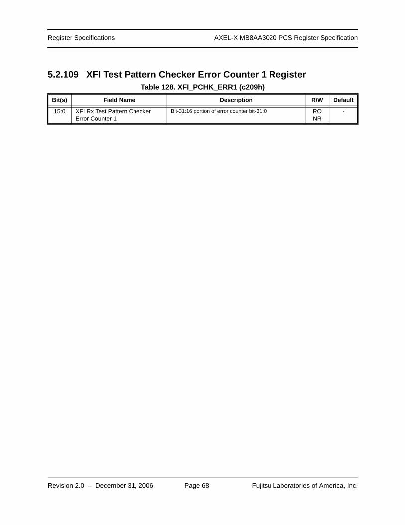
c209h RO XFI_PCHK_ERR1 XFI Test Pattern Checker Error Counter 1 Register
Table 19. XL Register OverviewAddress R/W Abbreviated Name Long Name
Page 25
Revision 2.0 – December 31, 2006 Page 25 Fujitsu Laboratories of America, Inc.
Register Specifications AXEL-X MB8AA3020 PCS Register Specification
5.2 Detailed Register Definitions
The registers are categorized into the following three groups.
• PCS: PCS registers which conform to IEEE 802.3ae subclause “45.2.3 PCS registers”. The address range is 0000h ~ 7fffh.
• PHY/XL: Vendor specific registers which are specific to PHY macro and XL logic which are used for 10GBASE-X(XAUI) and 10GBASE-R(XFI) in common. The address range is c000h ~ c0ffh.
• XAUI: Vendor specific registers which are specific to 10GBASE-X(XAUI). The address range is c100h ~ c1ffh.
• XFI: Vendor specific registers which are specific to 10GBASE-R(XFI). The address range is c200h ~ c2ffh.
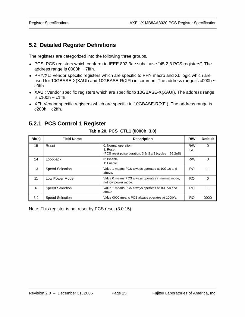
5.2.1 PCS Control 1 Register
Note: This register is not reset by PCS reset (3.0.15).
Table 20. PCS_CTL1 (0000h, 3.0)Bit(s) Field Name Description R/W Default
15 Reset 0: Normal operation1: Reset(PCS reset pulse duration: 3.2nS x 31cycles = 99.2nS)
R/WSC
0
14 Loopback 0: Disable1: Enable
R/W 0
13 Speed Selection Value 1 means PCS always operates at 10Gb/s and above.
RO 1
11 Low Power Mode Value 0 means PCS always operates in normal mode, not low power mode.
RO 0
6 Speed Selection Value 1 means PCS always operates at 10Gb/s and above.
RO 1
5:2 Speed Selection Value 0000 means PCS always operates at 10Gb/s. RO 0000
Page 26
Revision 2.0 – December 31, 2006 Page 26 Fujitsu Laboratories of America, Inc.
Register Specifications AXEL-X MB8AA3020 PCS Register Specification
5.2.2 PCS Status 1 Register
5.2.3 PCS Device Identifier 0 Register
5.2.4 PCS Device Identifier 1 Register
5.2.5 PCS Speed Ability Register
Table 21. PCS_STS1 (0001h, 3.1)Bit(s) Field Name Description R/W Default
7 Link Fault (before override) 0: Link up1: Link fault(This bit is logical-OR of 3.8.10 and 3.8.11.)
RO -
2 Receive Link Status 0: Receive link fault1: Receive link up(In 10GBASE-X mode, this bit is a latching low version of 3.24.12.)(In 10GBASE-R mode, this bit is a latching low version of 3.32.12.)
ROLL
-
1 Low Power Ability Value 0 means PCS doesn’t support low-power mode. RO 0
Table 22. PCS_DEV_ID0 (0002h, 3.2)Bit(s) Field Name Description R/W Default
15:0 PCS Device Identifier 0 Bit 15:0 portion of PCS device identifier bit-31:0The value comes from Core.
RO -
Table 23. PCS_DEV_ID1 (0003h, 3.3)Bit(s) Field Name Description R/W Default
15:0 PCS Device Identifier 1 Bit 31:16 portion of PCS device identifier bit-31:0The value comes from Core.
RO -
Table 24. PCS_SPEED (0004h, 3.4)Bit(s) Field Name Description R/W Default
0 10G Capable Value 1 means PCS is capable of operating at 10 Gb/s. RO 1
Page 27
Revision 2.0 – December 31, 2006 Page 27 Fujitsu Laboratories of America, Inc.
Register Specifications AXEL-X MB8AA3020 PCS Register Specification
5.2.6 PCS Device In Package 0 Register
5.2.7 PCS Device In Package 1 Register
5.2.8 PCS Control 2 Register
Note: This register is not reset by PCS reset (3.0.15).
Table 25. PCS_DEV_IN_PKG0 (0005h, 3.5)Bit(s) Field Name Description R/W Default
5 DTE XS Present Value 0 means DTE XS is not present. RO 0
4 PHY XS Present Value 0 means PHY XS is not present. RO 0
3 PCS Present Value 1 means PCS is present. RO 1
2 WIS Present Value 0 means WIS is not present. RO 0
1 PMA/PMD Present Value 0 means PMA/PMD are not present. RO 0
0 Clause 22 Registers Present Value 0 means Clause 22 registers are not present. RO 0
Table 26. PCS_DEV_IN_PKG1 (0006h, 3.6)Bit(s) Field Name Description R/W Default
15 Vendor Specific Device 2 Present Value 0 means Vendor Specific Device 2 is not present. RO 0
14 Vendor Specific Device 1 Present Value 0 means Vendor Specific Device 1 is not present. RO 0
Table 27. PCS_CTL2 (0007h, 3.7)Bit(s) Field Name Description R/W Default
1:0 Type Selection 00: Select 10GBASE-R PCS type (XFI)01: Select 10GBASE-X PCS type (XAUI)10: (Reserved)11: (Reserved)
R/W 01
Page 28
Revision 2.0 – December 31, 2006 Page 28 Fujitsu Laboratories of America, Inc.
Register Specifications AXEL-X MB8AA3020 PCS Register Specification
5.2.9 PCS Status 2 Register
5.2.10 PCS Package Identifier 0 Register
5.2.11 PCS Package Identifier 1 Register
Table 28. PCS_STS2 (0008h, 3.8)Bit(s) Field Name Description R/W Default
15:14 Device Present Value 10 means device is responding at this address. RO 10
11 Transmit Fault 0: No fault condition on transmit path1: Fault condition on transmit path
ROLH
-
10 Receive Fault 0: No fault condition on receive path1: Fault condition on receive path
ROLH
-
2 10GBASE-W Capable (WAN) Value 0 means PCS is not able to support 10GBASE-W PCS type (WAN).
RO 0
1 10GBASE-X Capable (XAUI) Value 1 means PCS is able to support 10GBASE-X PCS type (XAUI).
RO 1
0 10GBASE-R Capable (XFI) Value 1 means PCS is able to support 10GBASE-R PCS type (XF1).
RO 1
Table 29. PCS_PKG_ID0 (000eh, 3.14)Bit(s) Field Name Description R/W Default
15:0 Package Identifier 0 Bit-15:0 portion of package identifier bit-31:0 R0 0000h
Table 30. PCS_PKG_ID1 (000fh, 3.15)Bit(S) Field Name Description R/W Default
15:0 Package Identifier 1 Bit-31:16 portion of package identifier bit-31:0 RO 0000h
Page 29
Revision 2.0 – December 31, 2006 Page 29 Fujitsu Laboratories of America, Inc.
Register Specifications AXEL-X MB8AA3020 PCS Register Specification
5.2.12 PCS XAUI Status Register
5.2.13 PCS XAUI Test Control Register
5.2.14 PCS XFI Status 1 Register
Table 31. PCS_XAUI_STS (0018h, 3.24)Bit(s) Field Name Description R/W Default
12 XAUI Rx Lane Align Status (XAUI Receive Link Status)
0: XAUI Rx is not lane-aligned (link fault).1: XAUI Rx is lane-aligned (link up).
RO -
11 XAUI Tx Test Pattern Generator Ability
Value 1 means PCS is able to generate 10GBASE-X test patterns.
RO 1
3 XAUI Rx Lane-3 Comma Align Status
0: XAUI Rx Lane-3 is not comma-aligned.1: XAUI Rx Lane-3 is comma-aligned.
RO -
2 XAUI Rx Lane-2 Comma Align Status
0: XAUI Rx Lane-2 is not comma-aligned.1: XAUI Rx Lane-2 is comma-aligned.
RO -
1 XAUI Rx Lane-1 Comma Align Status
0: XAUI Rx Lane-1 is not comma-aligned.1: XAUI Rx Lane-1 is comma-aligned.
RO -
0 XAUI Rx Lane-0 Comma Align Status
0: XAUI Rx Lane-0 is not comma-aligned.1: XAUI Rx Lane-0 is comma-aligned.
RO -
Table 32. PCS_XAUI_TEST_CTL (0019h, 3.25)Bit(s) Field Name Description R/W Default
2 XAUI Tx Test Pattern Enable 0: Disable1: Enable
R/W 0
1:0 XAUI Tx Test Pattern Select 00: High frequency pattern (D21.5)01: Low frequency pattern (K28.7)10: Mixed frequency pattern (k28.5)11: (Reserved)
R/W 00
Table 33. PCS_XFI_STS1 (0020h, 3.32)Bit(s) Field Name Description R/W Default
12 XFI Receive Link Status 0: Link fault1: Link up
RO -
2 XFI PRBS31 Pattern Testing Ability
Value 1 means PCS is able to support 10GBASE-R PRBS31 pattern testing.
RO 1
1 XFI Rx High BER Status 0: Not high BER1: High BER
RO -
0 XFI Rx Block Lock Status 0: Not block-locked1: Block-locked
RO -
Page 30
Revision 2.0 – December 31, 2006 Page 30 Fujitsu Laboratories of America, Inc.
Register Specifications AXEL-X MB8AA3020 PCS Register Specification
5.2.15 PCS XFI Status 2 Register
5.2.16 PCS XFI Test Pattern Seed A0 Register
5.2.17 PCS XFI Test Pattern Seed A1 Register
5.2.18 PCS XFI Test Pattern Seed A2 Register
5.2.19 PCS XFI Test Pattern Seed A3 Register
Table 34. PCS_XFI_STS2 (0021h, 3.33)Bit(s) Field Name Description R/W Default
15 XFI Rx Block Lock Status 0: Not block-locked1: Block-locked(This bit is a latching low version of 3.32.0.)
ROLL
-
14 XFI Rx High BER Status 0: Not high BER1: High BER(This bit is a latching high version of 3.32.1.)
ROLH
-
13:8 XFI Rx BER Counter 6-bit BER counter value RCNR
-
7:0 XFI Rx Errored Block Counter 8-bit errored block counter value RCNR
-
Table 35. PCS_XFI_TEST_SEEDA0 (0022h, 3.34)Bit(s) Field Name Description R/W Default
15:0 XFI Test Pattern Seed A0 Bit-15:0 portion of XFI test pattern seed A bit-57:0 R/W 0000h
Table 36. PCS_XFI_TEST_SEEDA1 (0023h, 3.35)Bit(s) Field Name Description R/W Default
15:0 XFI Test Pattern Seed A1 Bit-31:16 Portion of XFI test pattern seed A bit-57:0 R/W 0000h
Table 37. PCS_XFI_TEST_SEEDA2 (0024h, 3.36)Bit(s) Field Name Description R/W Default
15:0 XFI Test Pattern Seed A2 Bit-47:32 portion of XFI test pattern seed A bit-57:0 R/W 0000h
Table 38. PCS_XFI_TEST_SEEDA3 (0025h, 3.37)Bit(s) Field Name Description R/W Default
9:0 XFI Test Pattern Seed A3 Bit-57:48 portion of XFI test pattern seed A bit-57:0 R/W 000h
Page 31
Revision 2.0 – December 31, 2006 Page 31 Fujitsu Laboratories of America, Inc.
Register Specifications AXEL-X MB8AA3020 PCS Register Specification
5.2.20 PCS XFI Test Pattern Seed B0 Register
5.2.21 PCS XFI Test Pattern Seed B1 Register
5.2.22 PCS XFI Test Pattern Seed B2 Register
5.2.23 PCS XFI Test Pattern Seed B3 Register
Table 39. PCS_XFI_TEST_SEEDB0 (0026h, 3.38)Bit(s) Field Name Description R/W Default
15:0 XFI Test Pattern Seed B0 Bit-15:0 portion of XFI test pattern seed B bit-57:0 R/W 0000h
Table 40. PCS_XFI_TEST_SEEDB1 (0027h, 3.39) Bit(3) Field Name Description R/W Default
15:0 XFI Test Pattern Seed B1 Bit-31:16 portion of XFI test pattern seed B bit-57:0 R/W 0000h
Table 41. PCS_XFI_TEST_SEEDB2 (0028h, 3.40)Bit(s) Field Name Description R/W Default
15:0 XFI Test Pattern Seed B2 Bit-47:32 portion of XFI test pattern seed B bit-57:0 R/W 0000h
Table 42. PCS_XFI_TEST_SEEDB3 (0029h, 3.41)Bit(s) Field Name Description R/W Default
9:0 XFI Test Pattern Seed B3 Bit-57:48 portion of XFI test pattern seed B bit-57:0 R/W 000h
Page 32
Revision 2.0 – December 31, 2006 Page 32 Fujitsu Laboratories of America, Inc.
Register Specifications AXEL-X MB8AA3020 PCS Register Specification
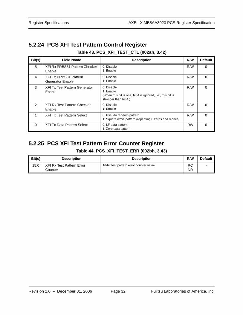
5.2.24 PCS XFI Test Pattern Control Register
5.2.25 PCS XFI Test Pattern Error Counter Register
Table 43. PCS_XFI_TEST_CTL (002ah, 3.42)Bit(s) Field Name Description R/W Default
5 XFI Rx PRBS31 Pattern Checker Enable
0: Disable1: Enable
R/W 0
4 XFI Tx PRBS31 PatternGenerator Enable
0: Disable1: Enable
R/W 0
3 XFI Tx Test Pattern Generator Enable
0: Disable1: Enable(When this bit is one, bit-4 is ignored, i.e., this bit is stronger than bit-4.)
R/W 0
2 XFI Rx Test Pattern Checker Enable
0: Disable1: Enable
R/W 0
1 XFI Tx Test Pattern Select 0: Pseudo random pattern1: Square wave pattern (repeating 8 zeros and 8 ones)
R/W 0
0 XFI Tx Data Pattern Select 0: LF data pattern1: Zero data pattern
RW 0
Table 44. PCS_XFI_TEST_ERR (002bh, 3.43)Bit(s) Description Description R/W Default
15:0 XFI Rx Test Pattern Error Counter
16-bit test pattern error counter value RCNR
-
Page 33
Revision 2.0 – December 31, 2006 Page 33 Fujitsu Laboratories of America, Inc.
Register Specifications AXEL-X MB8AA3020 PCS Register Specification
5.2.26 PHY Power Down Control Register
Note: This register is not reset by PCS reset (3.0.15).
Table 45. PHY_PWR_DOWN_CTL (c000h)Bit(s) Field Names Description R/W Default
15 User Power Down(I_USRPD)
0: Normal operation1: Power down
R/W 1
7 Rx Lane-3 Power Down(I_RX3CHPD)
0: Normal operation1: Power down
R/W 1
6 Rx Lane-2 Power Down(I_RX2CHPD)
0: Normal operation1: Power down
R/W 1
5 Rx Lane-1 Power Down(I_RX1CHPD)
0: Normal operation1: Power down
R/W 1
4 Rx Lane-0 Power Down(I_RX0CHPD)
0: Normal operation1: Power down
R/W 1
3 Tx Lane-3 Power Down(I_TX3CHPD)
0: Normal operation1: Power down
R/W 1
2 Tx Lane-2 Power Down(I_TX2CHPD)
0: Normal operation1: Power down
R/W 1
1 Tx Lane-1 Power Down(I_TX1CHPD)
0: Normal operation1: Power down
R/W 1
0 Tx Lane-0 Power Down(I_TX0CHPD)
0: Normal operation1: Power down
R/W 1
Page 34
Revision 2.0 – December 31, 2006 Page 34 Fujitsu Laboratories of America, Inc.
Register Specifications AXEL-X MB8AA3020 PCS Register Specification
5.2.27 PHY Current Bias Control Register
Note: This register is not reset by PCS reset (3.0.15).
Table 46. PHY_CURR_BIAS_CTL (c001h)Bit(s) Field Name Description R/W Default
9:8 PLL Current Bias Control Code(I_EVPLLIBCTL[1:0])
00: 25%01: 50%10: 75%11: 100%
R/W 10
6:4 Internal Current Bias Control Code(I_EVIBCTL[2:0])
000: -6%001: -2%010: -10%011: -6%100: 0%101: +4%110: -4%111: 0%
R/W 100
2:0 Phase Interpolator Current Bias Control Code(I_EVRXPIIBCTL[2:0])
000: -75%001: -50%010: -25%011: 0%100: +25%101: +50%110: +75%111: +100%
R/W 011
Page 35
Revision 2.0 – December 31, 2006 Page 35 Fujitsu Laboratories of America, Inc.
Register Specifications AXEL-X MB8AA3020 PCS Register Specification
5.2.28 XL Lane Polarity Swap Control Register
Note: This register is not reset by PCS reset (3.0.15).
Table 47. XL_LANE_SWAP_CTL (c002h)Bit(s) Field Names Description R/W Default
13:12 Rx Lane Swap 00: Lane 0 -> Lane-0, Lane-1 -> Lane-1, Lane-2 -> Lane-2, Lane-3 -> Lane-301: Lane 0 -> Lane-1, Lane-1 -> Lane-0, Lane-2 -> Lane-3, Lane-3 -> Lane-210: Lane 0 -> Lane-2, Lane-1 -> Lane-3, Lane-2 -> Lane-0, Lane-3 -> Lane-111: Lane 0 -> Lane-3, Lane-1 -> Lane-2, Lane-2 -> Lane-1, Lane-3 -> Lane-0
R/W 00
11 Rx Lane-3 Polarity Swap 0: Normal1: Polarity swap
R/W 0
10 Rx Lane-2 Polarity Swap 0: Normal1: Polarity swap
R/W 0
9 Rx Lane-1 Polarity Swap 0: Normal1: Polarity swap
R/W 0
8 Rx Lane-0 Polarity Swap 0: Normal1: Polarity swap
R/W 0
5:4 Tx Lane Swap 00: Lane 0 -> Lane-0, Lane-1 -> Lane-1, Lane-2 -> Lane-2, Lane-3 -> Lane-301: Lane 0 -> Lane-1, Lane-1 -> Lane-0, Lane-2 -> Lane-3, Lane-3 -> Lane-210: Lane 0 -> Lane-2, Lane-1 -> Lane-3, Lane-2 -> Lane-0, Lane-3 -> Lane-111: Lane 0 -> Lane-3, Lane-1 -> Lane-2, Lane-2 -> Lane-1, Lane-3 -> Lane-0
R/W 00
3 Tx Lane-3 Polarity Swap 0: Normal1: Polarity swap
R/W 0
2 Tx Lane-2 Polarity Swap 0: Normal1: Polarity swap
R/W 0
1 Tx Lane-1 Polarity Swap 0: Normal1: Polarity swap
R/W 0
0 Tx Lane-0 Polarity Swap 0: Normal1: Polarity swap
R/W 0
Page 36
Revision 2.0 – December 31, 2006 Page 36 Fujitsu Laboratories of America, Inc.
Register Specifications AXEL-X MB8AA3020 PCS Register Specification
5.2.29 PHY PLL Mode Control Register
Note: This register is not reset by PCS reset (3.0.15).
Table 48. PHY_PLL_MODE_CTL (c003h)Bit(s) Field Name Description R/W Default
15 PLL Mode Setting Override Enable
0: Disable1: Enable
R/W 0
11:9 Divider Ratio for PLL (B) (I_PLLDIVSET[2:0])
000: (Reserved)001: (Reserved010: (Reserved)011: 1/40100: 1/33101: (Reserved)110: (Reserved)111: (Reserved)
R/W 011
8:6 Divider Ratio for Gear Box Clock (D)(I_PLLDIVCLKASET[2:0])
000: (Reserved)001: 1/16010: 1/32011: (Reserved)100: (Reserved)101: (Reserved)110: (Reserved)111: (Reserved)
R/W 010
5:4 Divider Ratio for Skewless Clock Tree (C)(I_PLLSPDSET[1:0])
00: 1/101: (Reserved)10: 1/411: (Reserved)
R/W 10
3:0 PLL Output Clock Frequency Fine Tune(I_PLLCTL[3:0])
0000: Maximum:
1111: Minimum
R/W 0101
Page 37
Revision 2.0 – December 31, 2006 Page 37 Fujitsu Laboratories of America, Inc.
Register Specifications AXEL-X MB8AA3020 PCS Register Specification
5.2.30 PHY Tx Mode Control Register
Note: This register is not reset by PCS reset (3.0.15).
Table 49. PHY_TX_MODE_CTL (c004h)Bit(s) Field Name Description R/W Default
15 Tx Mode Setting Override Enable 0: Disable1: Enable
R/W 0
5:4 Tx Parallel Data Input Width(I_TXPWID[1:0])
00: 32-bit01: 16-bit10: (Reserved)11: (Reserved)
R/W 01
3 Tx Lane-3 Clock Divider Slave Mode(I_TX3MXDIVSLV)
0: Master1: Slave
R/W 1
2 Tx Lane-2 Clock Divider Slave Mode(I_TX2MXDIVSLV)
0: Master1: Slave
R/W 1
1 Tx Lane-1 Clock Divider Slave Mode(I_TX1MXDIVSLV)
0: Master1: Slave
R/W 1
0 Tx Lane-0 Clock Divider Slave Mode(I_TX0MXDIVSLV)
0: Master1: Slave
R/W 0
Page 38
Revision 2.0 – December 31, 2006 Page 38 Fujitsu Laboratories of America, Inc.
Register Specifications AXEL-X MB8AA3020 PCS Register Specification
5.2.31 PHY Rx Mode Control Register
Note: This register is not reset by PCS reset (3.0.15).
Table 50. PHY_RX_MODE_CTL (c005h)Bit(s) Field Name Description R/W Default
15 Rx Mode Setting Override Enable
0: Disable1: Enable
R/W 0
13:12 Rx Parallel Data Output Width(I_RXPWID[1:0])
00: 32-bit01: 16-bit10: (Reserved)t11: (Reserved)
R/W 01
10:8 Rx PCLKA Divider Ratio(I_RXPCLKASET[2:0])
000: 1/33001: (Reserved)010: (Reserved)011: 1/5100: (Reserved101: (Reserved)110: (Reserved)111: (Reserved)
R/W 011
7:6 Rx Lane-3 Equalizer SpeedControl(I_RX3EQSPD[1:0])
00: XFI01: (Reserved)10: XAUI11: (Reserved)
R/W 10
5:4 Rx Lane-2 Equalizer SpeedControl(I_RX2EQSPD[1:0])
00: XFI01: (Reserved)10: XAUI11: (Reserved)
R/W 10
3:2 Rx Lane-1 Equalizer SpeedControl(I_RX1EQSPD[1:0])
00: XFI01: (Reserved)10: XAUI11: (Reserved)
R/W 10
1:0 Rx Lane-0 Equalizer SpeedControl(I_RX0EQSPD[1:0])
00: XFI01: (Reserved)10: XAUI11: (Reserved)
R/W 10
Page 39
Revision 2.0 – December 31, 2006 Page 39 Fujitsu Laboratories of America, Inc.
Register Specifications AXEL-X MB8AA3020 PCS Register Specification
5.2.32 PHY Lock Control Register
Note: This register is not reset by PCS reset (3.0.15).
Table 51. PHY_LOCK_CTL (c006h)Bit(s) Field Name Description R/W Default
7 Tx Lane-3 Synchronizer Lock Detection Status(O_TX3LOCK)
0: Not locked1: Locked
RO -
6 Tx Lane-2 Synchronizer Lock Detection Status(O_TX2LOCK)
0: Not locked1: Locked
RO -
5 Tx Lane-1 Synchronizer Lock Detection Status(O_TX1LOCK)
0: Not locked1: Locked
RO -
4 Tx Lane-0 Synchronizer Lock Detection Status(O_TX0LOCK)
0: Not locked1: Locked
RO -
3 Tx Lane-3 Synchronizer Lock Hold(I_TX3LOCKED)
0: Automatically re-start process of obtaining lock when lock is lost.1: Hold lock once locked.
R/W 0
2 Tx Lane-2 Synchronizer Lock Hold(I_TX2LOCKED)
0: Automatically re-start process of obtaining lock when lock is lost.1: Hold lock once locked.
R/W 0
1 Tx Lane-1 Synchronizer Lock Hold(I_TX1LOCKED)
0: Automatically re-start process of obtaining lock when lock is lost.1: Hold lock once locked.
R/W 0
0 Tx Lane-0 Synchronizer Lock Hold(I_TX0LOCKED)
0: Automatically re-start process of obtaining lock when lock is lost.1: Hold lock once locked.
R/W 0
Page 40
Revision 2.0 – December 31, 2006 Page 40 Fujitsu Laboratories of America, Inc.
Register Specifications AXEL-X MB8AA3020 PCS Register Specification
5.2.33 PHY CDR Control Register
Note: This register is not reset by PCS reset (3.0.15).
Table 52. PHY_CDR_CTL (c007h)Bit(s) Field Size Description R/W Default
14 Phase Interpolator Phase Code Control(I_EVRXPICODESEL)
0: Normal operation1: Code fixed
R/W 0
13:8 Phase Interpolator Phase Code(I_EVRXPICODE[5:0])
000000: Minimum:
111111: Maximum
R/W 000000
7 Digital Filter Clock Select(I_RXDFCLKSEL)
0: Internal1: External (I_RXnDFCLK)
R/W 0
6 Digital Filter Output Code Control(I_RXDFMSEL)
0: Decrement1: Increment
R/W 0
5:3 Digital Filter G2 Code(I_EVRXDFG2SET[2:0])
000: Minimum:
111: Maximum
R/W 011
2:0 Digital Filter G1 Code(I_EVRXDFG1SET[2:0])
000: Minimum:
111: Maximum
R/W 010
Page 41
Revision 2.0 – December 31, 2006 Page 41 Fujitsu Laboratories of America, Inc.
Register Specifications AXEL-X MB8AA3020 PCS Register Specification
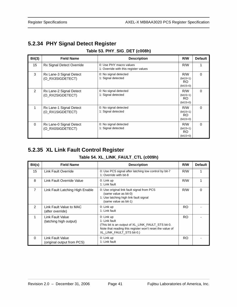
5.2.34 PHY Signal Detect Register
5.2.35 XL Link Fault Control Register
Table 53. PHY_SIG_DET (c008h)Bit(3) Field Name Description R/W Default
15 Rx Signal Detect Override 0: Use PHY macro values1: Override with this register values
R/W 1
3 Rx Lane-3 Signal Detect(O_RX3SIGDETECT)
0: No signal detected1: Signal detected
R/W(bit15=1)
RO(bit15=0)
0
2 Rx Lane-2 Signal Detect(O_RX2SIGDETECT)
0: No signal detected1: Signal detected
R/W(bit15=1)
RO(bit15=0)
0
1 Rx Lane-1 Signal Detect(O_RX1SIGDETECT)
0: No signal detected1: Signal detected
R/W(bit15=1)
RO(bit15=0)
0
0 Rx Lane-0 Signal Detect(O_RX0SIGDETECT)
0: No signal detected1: Signal detected
R/W(bit15=1)
RO(bit15=0)
0
Table 54. XL_LINK_FAULT_CTL (c009h)Bit(s) Field Name Description R/W Default
15 Link Fault Override 0: Use PCS signal after latching low control by bit-71: Override with bit-8
R/W 1
8 Link Fault Override Value 0: Link up1: Link fault
R/W 1
7 Link Fault Latching High Enable 0: Use original link fault signal from PCS (same value as bit-0)1: Use latching high link fault signal (same value as bit-1)
R/W 0
2 Link Fault Value to MAC(after override)
0: Link up1: Link fault
RO -
1 Link Fault Value(latching high output)
0: Link up1: Link fault(This bit is an output of XL_LINK_FAULT_STS bit-0. Note that reading this register won’t reset the value of XL_LINK_FAULT_STS bit-0.)
RO -
0 Link Fault Value(original output from PCS)
0: Link up1: Link fault
RO -
Page 42
Revision 2.0 – December 31, 2006 Page 42 Fujitsu Laboratories of America, Inc.
Register Specifications AXEL-X MB8AA3020 PCS Register Specification
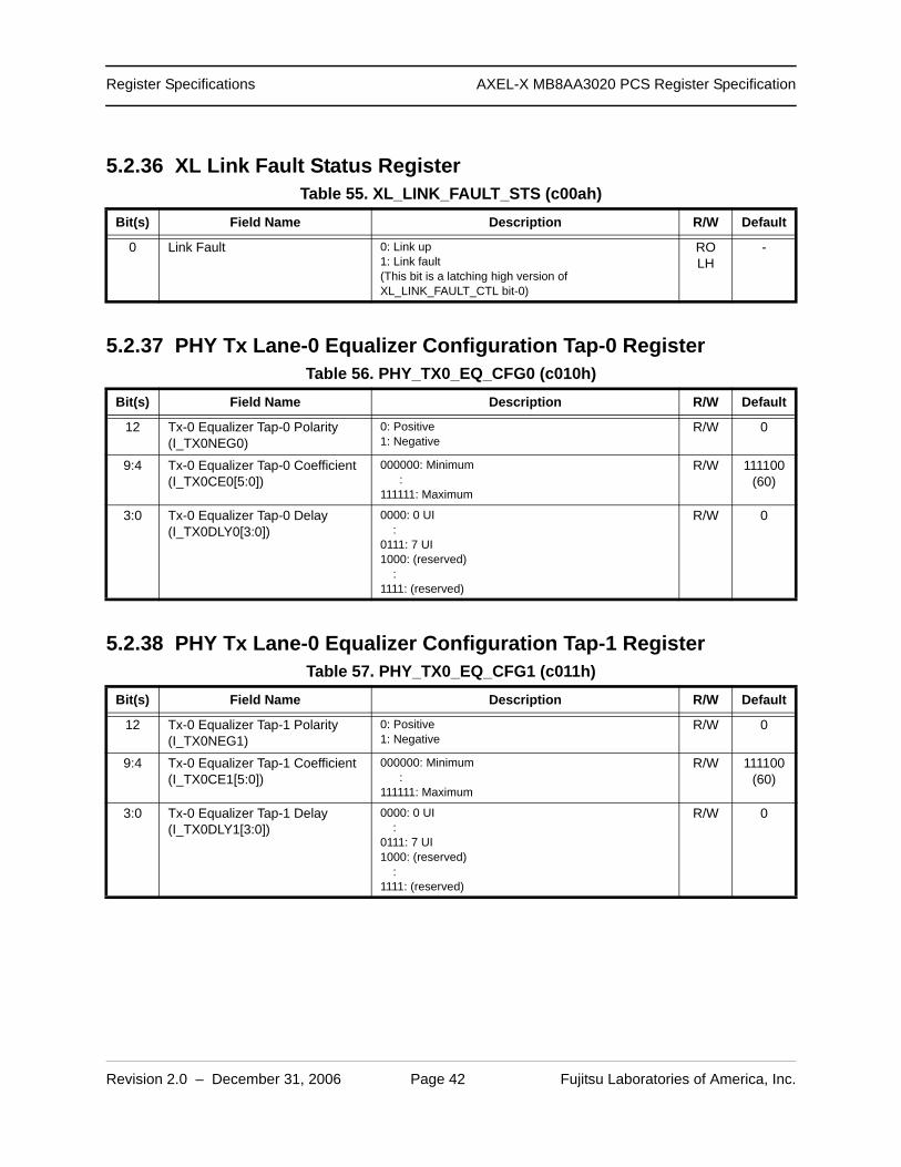
5.2.36 XL Link Fault Status Register
5.2.37 PHY Tx Lane-0 Equalizer Configuration Tap-0 Register
5.2.38 PHY Tx Lane-0 Equalizer Configuration Tap-1 Register
Table 55. XL_LINK_FAULT_STS (c00ah)Bit(s) Field Name Description R/W Default
0 Link Fault 0: Link up1: Link fault(This bit is a latching high version of XL_LINK_FAULT_CTL bit-0)
ROLH
-
Table 56. PHY_TX0_EQ_CFG0 (c010h)Bit(s) Field Name Description R/W Default
12 Tx-0 Equalizer Tap-0 Polarity(I_TX0NEG0)
0: Positive1: Negative
R/W 0
9:4 Tx-0 Equalizer Tap-0 Coefficient(I_TX0CE0[5:0])
000000: Minimum:
111111: Maximum
R/W 111100(60)
3:0 Tx-0 Equalizer Tap-0 Delay(I_TX0DLY0[3:0])
0000: 0 UI:
0111: 7 UI1000: (reserved)
:1111: (reserved)
R/W 0
Table 57. PHY_TX0_EQ_CFG1 (c011h)Bit(s) Field Name Description R/W Default
12 Tx-0 Equalizer Tap-1 Polarity(I_TX0NEG1)
0: Positive1: Negative
R/W 0
9:4 Tx-0 Equalizer Tap-1 Coefficient(I_TX0CE1[5:0])
000000: Minimum:
111111: Maximum
R/W 111100(60)
3:0 Tx-0 Equalizer Tap-1 Delay(I_TX0DLY1[3:0])
0000: 0 UI:
0111: 7 UI1000: (reserved)
:1111: (reserved)
R/W 0
Page 43
Revision 2.0 – December 31, 2006 Page 43 Fujitsu Laboratories of America, Inc.
Register Specifications AXEL-X MB8AA3020 PCS Register Specification
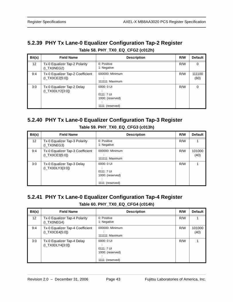
5.2.39 PHY Tx Lane-0 Equalizer Configuration Tap-2 Register
5.2.40 PHY Tx Lane-0 Equalizer Configuration Tap-3 Register
5.2.41 PHY Tx Lane-0 Equalizer Configuration Tap-4 Register
Table 58. PHY_TX0_EQ_CFG2 (c012h)Bit(s) Field Name Description R/W Default
12 Tx-0 Equalizer Tap-2 Polarity(I_TX0NEG2)
0: Positive1: Negative
R/W 0
9:4 Tx-0 Equalizer Tap-2 Coefficient(I_TX0CE2[5:0])
000000: Minimum:
111111: Maximum
R/W 111100(60)
3:0 Tx-0 Equalizer Tap-2 Delay(I_TX0DLY2[3:0])
0000: 0 UI:
0111: 7 UI1000: (reserved)
:1111: (reserved)
R/W 0
Table 59. PHY_TX0_EQ_CFG3 (c013h)Bit(s) Field Name Description R/W Default
12 Tx-0 Equalizer Tap-3 Polarity(I_TX0NEG3)
0: Positive1: Negative
R/W 1
9:4 Tx-0 Equalizer Tap-3 Coefficient(I_TX0CE3[5:0])
000000: Minimum:
111111: Maximum
R/W 101000(40)
3:0 Tx-0 Equalizer Tap-3 Delay(I_TX0DLY3[3:0])
0000: 0 UI:
0111: 7 UI1000: (reserved)
:1111: (reserved)
R/W 1
Table 60. PHY_TX0_EQ_CFG4 (c014h)Bit(s) Field Name Description R/W Default
12 Tx-0 Equalizer Tap-4 Polarity(I_TX0NEG4)
0: Positive1: Negative
R/W 1
9:4 Tx-0 Equalizer Tap-4 Coefficient(I_TX0CE4[5:0])
000000: Minimum:
111111: Maximum
R/W 101000(40)
3:0 Tx-0 Equalizer Tap-4 Delay(I_TX0DLY4[3:0])
0000: 0 UI:
0111: 7 UI1000: (reserved)
:1111: (reserved)
R/W 1
Page 44
Revision 2.0 – December 31, 2006 Page 44 Fujitsu Laboratories of America, Inc.
Register Specifications AXEL-X MB8AA3020 PCS Register Specification
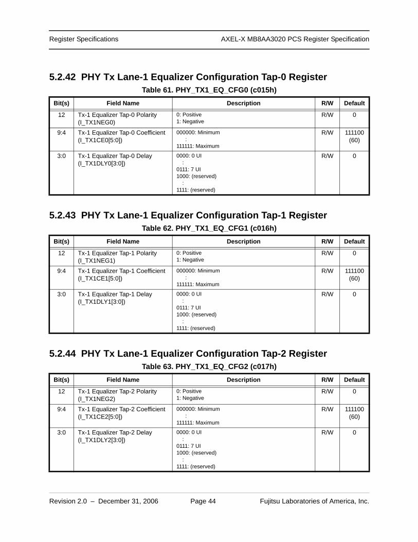
5.2.42 PHY Tx Lane-1 Equalizer Configuration Tap-0 Register
5.2.43 PHY Tx Lane-1 Equalizer Configuration Tap-1 Register
5.2.44 PHY Tx Lane-1 Equalizer Configuration Tap-2 Register
Table 61. PHY_TX1_EQ_CFG0 (c015h)Bit(s) Field Name Description R/W Default
12 Tx-1 Equalizer Tap-0 Polarity(I_TX1NEG0)
0: Positive1: Negative
R/W 0
9:4 Tx-1 Equalizer Tap-0 Coefficient(I_TX1CE0[5:0])
000000: Minimum:
111111: Maximum
R/W 111100(60)
3:0 Tx-1 Equalizer Tap-0 Delay(I_TX1DLY0[3:0])
0000: 0 UI:
0111: 7 UI1000: (reserved)
:1111: (reserved)
R/W 0
Table 62. PHY_TX1_EQ_CFG1 (c016h)Bit(s) Field Name Description R/W Default
12 Tx-1 Equalizer Tap-1 Polarity(I_TX1NEG1)
0: Positive1: Negative
R/W 0
9:4 Tx-1 Equalizer Tap-1 Coefficient(I_TX1CE1[5:0])
000000: Minimum:
111111: Maximum
R/W 111100(60)
3:0 Tx-1 Equalizer Tap-1 Delay(I_TX1DLY1[3:0])
0000: 0 UI:
0111: 7 UI1000: (reserved)
:1111: (reserved)
R/W 0
Table 63. PHY_TX1_EQ_CFG2 (c017h)Bit(s) Field Name Description R/W Default
12 Tx-1 Equalizer Tap-2 Polarity(I_TX1NEG2)
0: Positive1: Negative
R/W 0
9:4 Tx-1 Equalizer Tap-2 Coefficient(I_TX1CE2[5:0])
000000: Minimum:
111111: Maximum
R/W 111100(60)
3:0 Tx-1 Equalizer Tap-2 Delay(I_TX1DLY2[3:0])
0000: 0 UI:
0111: 7 UI1000: (reserved)
:1111: (reserved)
R/W 0
Page 45
Revision 2.0 – December 31, 2006 Page 45 Fujitsu Laboratories of America, Inc.
Register Specifications AXEL-X MB8AA3020 PCS Register Specification
5.2.45 PHY Tx Lane-1 Equalizer Configuration Tap-3 Register
5.2.46 PHY Tx Lane-1 Equalizer Configuration Tap-4 Register
5.2.47 PHY Tx Lane-2 Equalizer Configuration Tap-0 Register
Table 64. PHY_TX1_EQ_CFG3 (c018h)Bit(s) Field Name Description R/W Default
12 Tx-1 Equalizer Tap-3 Polarity(I_TX1NEG3)
0: Positive1: Negative
R/W 1
9:4 Tx-1 Equalizer Tap-3 Coefficient(I_TX1CE3[5:0])
000000: Minimum:
111111: Maximum
R/W 101000(40)
3:0 Tx-1 Equalizer Tap-3 Delay(I_TX1DLY3[3:0])
0000: 0 UI:
0111: 7 UI1000: (reserved)
:1111: (reserved)
R/W 1
Table 65. PHY_TX1_EQ_CFG4 (c019h)Bit(s) Field Name Description R/W Default
12 Tx-1 Equalizer Tap-4 Polarity(I_TX1NEG4)
0: Positive1: Negative
R/W 1
9:4 Tx-1 Equalizer Tap-4 Coefficient(I_TX1CE4[5:0])
000000: Minimum:
111111: Maximum
R/W 101000(40)
3:0 Tx-1 Equalizer Tap-4 Delay(I_TX1DLY4[3:0])
0000: 0 UI:
0111: 7 UI1000: (reserved)
:1111: (reserved)
R/W 1
Table 66. PHY_TX2_EQ_CFG0 (c01ah)Bit(s) Field Name Description R/W Default
12 Tx-2 Equalizer Tap-0 Polarity(I_TX2NEG0)
0: Positive1: Negative
R/W 0
9:4 Tx-2 Equalizer Tap-0 Coefficient(I_TX2CE0[5:0])
000000: Minimum:
111111: Maximum
R/W 111100(60)
3:0 Tx-2 Equalizer Tap-0 Delay(I_TX2DLY0[3:0])
0000: 0 UI:
0111: 7 UI1000: (reserved)
:1111: (reserved)
R/W 0
Page 46
Revision 2.0 – December 31, 2006 Page 46 Fujitsu Laboratories of America, Inc.
Register Specifications AXEL-X MB8AA3020 PCS Register Specification
5.2.48 PHY Tx Lane-2 Equalizer Configuration Tap-1 Register
5.2.49 PHY Tx Lane-2 Equalizer Configuration Tap-2 Register
5.2.50 PHY Tx Lane-2 Equalizer Configuration Tap-3 Register
Table 67. PHY_TX2_EQ_CFG1 (c01bh)Bit(s) Field Name Description R/W Default
12 Tx-2 Equalizer Tap-1 Polarity(I_TX2NEG1)
0: Positive1: Negative
R/W 0
9:4 Tx-2 Equalizer Tap-1 Coefficient(I_TX2CE1[5:0])
000000: Minimum:
111111: Maximum
R/W 111100(60)
3:0 Tx-2 Equalizer Tap-1 Delay(I_TX2DLY1[3:0])
0000: 0 UI:
0111: 7 UI1000: (reserved)
:1111: (reserved)
R/W 0
Table 68. PHY_TX2_EQ_CFG2 (c01ch)Bit(s) Field Name Description R/W Default
12 Tx-2 Equalizer Tap-2 Polarity(I_TX2NEG2)
0: Positive1: Negative
R/W 0
9:4 Tx-2 Equalizer Tap-2 Coefficient(I_TX2CE2[5:0])
000000: Minimum:
111111: Maximum
R/W 111100(60)
3:0 Tx-2 Equalizer Tap-2 Delay(I_TX2DLY2[3:0])
0000: 0 UI:
0111: 7 UI1000: (reserved)
:1111: (reserved)
R/W 0
Table 69. PHY_TX2_EQ_CFG3 (c01dh)Bit(s) Field Name Description R/W Default
12 Tx-2 Equalizer Tap-3 Polarity(I_TX2NEG3)
0: Positive1: Negative
R/W 1
9:4 Tx-2 Equalizer Tap-3 Coefficient(I_TX2CE3[5:0])
000000: Minimum:
111111: Maximum
R/W 101000(40)
3:0 Tx-2 Equalizer Tap-3 Delay(I_TX2DLY3[3:0])
0000: 0 UI:
0111: 7 UI1000: (reserved)
:1111: (reserved)
R/W 1
Page 47
Revision 2.0 – December 31, 2006 Page 47 Fujitsu Laboratories of America, Inc.
Register Specifications AXEL-X MB8AA3020 PCS Register Specification
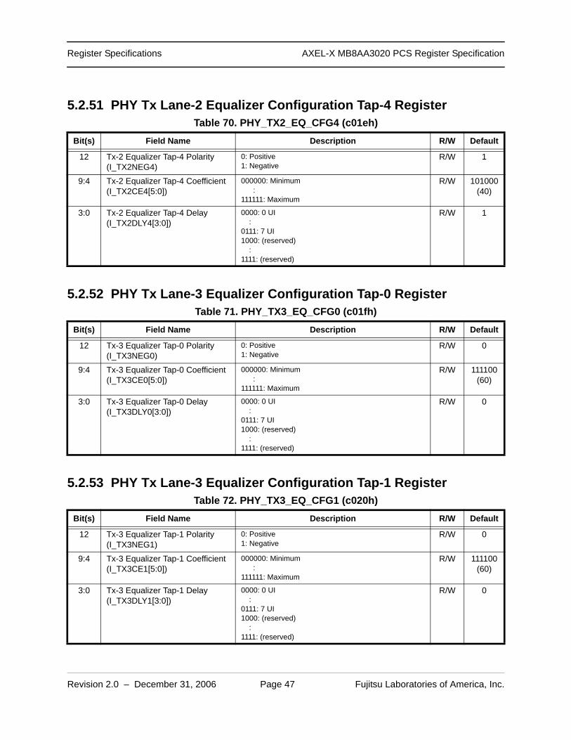
5.2.51 PHY Tx Lane-2 Equalizer Configuration Tap-4 Register
5.2.52 PHY Tx Lane-3 Equalizer Configuration Tap-0 Register
5.2.53 PHY Tx Lane-3 Equalizer Configuration Tap-1 Register
Table 70. PHY_TX2_EQ_CFG4 (c01eh)Bit(s) Field Name Description R/W Default
12 Tx-2 Equalizer Tap-4 Polarity(I_TX2NEG4)
0: Positive1: Negative
R/W 1
9:4 Tx-2 Equalizer Tap-4 Coefficient(I_TX2CE4[5:0])
000000: Minimum:
111111: Maximum
R/W 101000(40)
3:0 Tx-2 Equalizer Tap-4 Delay(I_TX2DLY4[3:0])
0000: 0 UI:
0111: 7 UI1000: (reserved)
:1111: (reserved)
R/W 1
Table 71. PHY_TX3_EQ_CFG0 (c01fh)Bit(s) Field Name Description R/W Default
12 Tx-3 Equalizer Tap-0 Polarity(I_TX3NEG0)
0: Positive1: Negative
R/W 0
9:4 Tx-3 Equalizer Tap-0 Coefficient(I_TX3CE0[5:0])
000000: Minimum:
111111: Maximum
R/W 111100(60)
3:0 Tx-3 Equalizer Tap-0 Delay(I_TX3DLY0[3:0])
0000: 0 UI:
0111: 7 UI1000: (reserved)
:1111: (reserved)
R/W 0
Table 72. PHY_TX3_EQ_CFG1 (c020h)Bit(s) Field Name Description R/W Default
12 Tx-3 Equalizer Tap-1 Polarity(I_TX3NEG1)
0: Positive1: Negative
R/W 0
9:4 Tx-3 Equalizer Tap-1 Coefficient(I_TX3CE1[5:0])
000000: Minimum:
111111: Maximum
R/W 111100(60)
3:0 Tx-3 Equalizer Tap-1 Delay(I_TX3DLY1[3:0])
0000: 0 UI:
0111: 7 UI1000: (reserved)
:1111: (reserved)
R/W 0
Page 48
Revision 2.0 – December 31, 2006 Page 48 Fujitsu Laboratories of America, Inc.
Register Specifications AXEL-X MB8AA3020 PCS Register Specification
5.2.54 PHY Tx Lane-3 Equalizer Configuration Tap-2 Register
5.2.55 PHY Tx Lane-3 Equalizer Configuration Tap-3 Register
5.2.56 PHY Tx Lane-3 Equalizer Configuration Tap-4 Register
Table 73. PHY_TX3_EQ_CFG2 (c021h)Bit(s) Field Name Description R/W Default
12 Tx-3 Equalizer Tap-2 Polarity(I_TX3NEG2)
0: Positive1: Negative
R/W 0
9:4 Tx-3 Equalizer Tap-2 Coefficient(I_TX3CE2[5:0])
000000: Minimum:
111111: Maximum
R/W 111100(60)
3:0 Tx-3 Equalizer Tap-2 Delay(I_TX3DLY2[3:0])
0000: 0 UI:
0111: 7 UI1000: (reserved)
:1111: (reserved)
R/W 0
Table 74. PHY_TX3_EQ_CFG3 (c022h)Bit(s) Field Name Description R/W Default
12 Tx-3 Equalizer Tap-3 Polarity(I_TX3NEG3)
0: Positive1: Negative
R/W 1
9:4 Tx-3 Equalizer Tap-3 Coefficient(I_TX3CE3[5:0])
000000: Minimum:
111111: Maximum
R/W 101000(40)
3:0 Tx-3 Equalizer Tap-3 Delay(I_TX3DLY3[3:0])
0000: 0 UI:
0111: 7 UI1000: (reserved)
:1111: (reserved)
R/W 1
Table 75. PHY_TX3_EQ_CFG4 (c023h)Bit(s) Field Name Description R/W Default
12 Tx-3 Equalizer Tap-4 Polarity(I_TX3NEG4)
0: Positive1: Negative
R/W 1
9:4 Tx-3 Equalizer Tap-4 Coefficient(I_TX3CE4[5:0])
000000: Minimum:
111111: Maximum
R/W 101000(40)
3:0 Tx-3 Equalizer Tap-4 Delay(I_TX3DLY4[3:0])
0000: 0 UI:
0111: 7 UI1000: (reserved)
:1111: (reserved)
R/W 1
Page 49
Revision 2.0 – December 31, 2006 Page 49 Fujitsu Laboratories of America, Inc.
Register Specifications AXEL-X MB8AA3020 PCS Register Specification
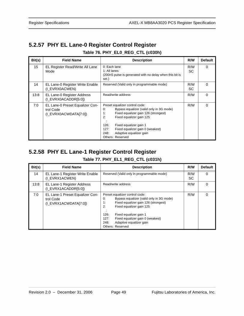
5.2.57 PHY EL Lane-0 Register Control Register
5.2.58 PHY EL Lane-1 Register Control Register
Table 76. PHY_EL0_REG_CTL (c030h)Bit(s) Field Name Description R/W Default
15 EL Register Read/Write All Lane Mode
0: Each lane1: All lanes(200nS pulse is generated with no delay when this bit is set.)
R/WSC
0
14 EL Lane-0 Register Write Enable(I_EVRX0ACWEN)
Reserved (Valid only in programmable mode) R/WSC
0
13:8 EL Lane-0 Register Address(I_EVRX0ACADDR[5:0])
Read/write address R/W 0
7:0 EL Lane-0 Preset Equalizer Con-trol Code(I_EVRX0ACWDATA[7:0])
Preset equalizer control code:0: Bypass equalizer (valid only in 3G mode)1: Fixed equalizer gain 126 (strongest)2: Fixed equalizer gain 125
:126: Fixed equalizer gain 1127: Fixed equalizer gain 0 (weakest)248: Adaptive equalizer gainOthers: Reserved
R/W 0
Table 77. PHY_EL1_REG_CTL (c031h)Bit(s) Field Name Description R/W Default
14 EL Lane-1 Register Write Enable(I_EVRX1ACWEN)
Reserved (Valid only in programmable mode) R/WSC
0
13:8 EL Lane-1 Register Address(I_EVRX1ACADDR[5:0])
Read/write address R/W 0
7:0 EL Lane-1 Preset Equalizer Con-trol Code(I_EVRX1ACWDATA[7:0])
Preset equalizer control code:0: Bypass equalizer (valid only in 3G mode)1: Fixed equalizer gain 126 (strongest)2: Fixed equalizer gain 125
:126: Fixed equalizer gain 1127: Fixed equalizer gain 0 (weakest)248: Adaptive equalizer gainOthers: Reserved
R/W 0
Page 50
Revision 2.0 – December 31, 2006 Page 50 Fujitsu Laboratories of America, Inc.
Register Specifications AXEL-X MB8AA3020 PCS Register Specification
5.2.59 PHY EL Lane-2 Register Control Register
5.2.60 PHY EL Lane-3 Register Control Register
5.2.61 PHY EL Lane-01 Register Read Register
Table 78. PHY_EL2_REG_CTL (c032h)Bit(s) Field Name Description R/W Default
14 EL Lane-2 Register Write Enable(I_EVRX2ACWEN)
Reserved (Valid only in programmable mode) R/WSC
0
13:8 EL Lane-2 Register Address(I_EVRX2ACADDR[5:0])
Read/write address R/W 0
7:0 EL Lane-2 Preset Equalizer Con-trol Code(I_EVRX2ACWDATA[7:0])
Preset equalizer control code:0: Bypass equalizer (valid only in 3G mode)1: Fixed equalizer gain 126 (strongest)2: Fixed equalizer gain 125
:126: Fixed equalizer gain 1127: Fixed equalizer gain 0 (weakest)248: Adaptive equalizer gainOthers: Reserved
R/W 0
Table 79. PHY_EL3_REG_CTL (c033h)Bit(s) Field Name Description R/W Default
14 EL Lane-3 Register Write Enable(I_EVRX3ACWEN)
Reserved (Valid only in programmable mode) R/WSC
0
13:8 EL Lane-3 Register Address(I_EVRX3ACADDR[5:0])
Read/write address R/W 0
7:0 EL Lane-3 Preset Equalizer Con-trol Code(I_EVRX3ACWDATA[7:0])
Preset equalizer control code:0: Bypass equalizer (valid only in 3G mode)1: Fixed equalizer gain 126 (strongest)2: Fixed equalizer gain 125
:126: Fixed equalizer gain 1127: Fixed equalizer gain 0 (weakest)248: Adaptive equalizer gainOthers: Reserved
R/W 0
Table 80. PHY_EL01_REG_READ (c034h)Bit(s) Field Name Description R/W Default
15:8 EL Lane-1 Register Read Data(O_EVRX1ACRDATA[7:0])
Lane-1 read data RO -
7:0 EL Lane-0 Register Read Data(O_EVRX0ACRDATA[7:0])
Lane-0 read data RO -
Page 51
Revision 2.0 – December 31, 2006 Page 51 Fujitsu Laboratories of America, Inc.
Register Specifications AXEL-X MB8AA3020 PCS Register Specification
5.2.62 PHY EL Lane-23 Register Read Register
5.2.63 PHY EL Mode Control Register
Table 81. PHY_EL23_REG_READ (c035h)Bit(s) Field Name Description R/W Default
15:8 EL Lane-3 Register Read Data(O_EVRX3ACRDATA[7:0])
Lane-3 read data RO -
7:0 EL Lane-2 Register Read Data(O_EVRX2ACRDATA[7:0])
Lane-2 read data RO -
Table 82. PHY_EL_MODE_CTL (c036h)Bit(s) Field Name Description R/W Default
5 EL Adaptation Restart(I_RX0ACRSTX)(I_RX1ACRSTX)(I_RX2ACRSTX)(I_RX3ACRSTX)
0: No action 1: Restart adaptation control by setting 1st order path gain to the initial value(100nS pulse is generated with no delay when this bit is set.)
R/W SC
0
4 EL Reserved Bit(I_RX0ACMODE[4])(I_RX1ACMODE[4])(I_RX2ACMODE[4])(I_RX3ACMODE[4])
Reserved bit R/W 0
3 EL Loop Constant Boost Enable(I_RX0ACMODE[3])(I_RX1ACMODE[3])(I_RX2ACMODE[3])(I_RX3ACMODE[3])
0: Disable1: Enable
R/W 0
2 EL Gain Control Enable(I_RX0ACMODE[2])(I_RX1ACMODE[2])(I_RX2ACMODE[2])(I_RX3ACMODE[2])
0: Disable1: Enable
R/W 0
1 EL Offset Cancel Enable(I_RX0ACMODE[1])(I_RX1ACMODE[1])(I_RX2ACMODE[1])(I_RX3ACMODE[1])
0: Disable1: Enable
R/W 0
0 EL Operation Mode(I_RX0ACMODE[0])(I_RX1ACMODE[0])(I_RX2ACMODE[0])(I_RX3ACMODE[0])
0: Preset Mode1: Reserved (Programmable mode)
R/W 0
Page 52
Revision 2.0 – December 31, 2006 Page 52 Fujitsu Laboratories of America, Inc.
Register Specifications AXEL-X MB8AA3020 PCS Register Specification
5.2.64 PHY EL Test Control Register
5.2.65 PHY Test Pattern Generator Control Register
Table 83. PHY_EL_TEST_CTL (c037h)Bit(s) Field Name Description R/W Default
5 EL Event Counter Clear(I_EVRX0ACCNTCLRX) (I_EVRX1ACCNTCLRX) (I_EVRX2ACCNTCLRX) (I_EVRX3ACCNTCLRX)
0: No action 1: Clear(100nS pulse is generated with no delay when this bit is set.)
R/WSC
0
4 EL Event Counter Enable 2(I_EVRX0ACCNTEN)(I_EVRX1ACCNTEN)(I_EVRX2ACCNTEN)(I_EVRX3ACCNTEN)
0: Disable1: Enable(393.216uS pulse is generated with 100nS delay when this bit is set and ORed with bit-3 value, then sent to PHY.)
R/WSC
0
3 EL Event Counter Enable 1(I_EVRX0ACCNTEN)(I_EVRX1ACCNTEN)(I_EVRX2ACCNTEN)(I_EVRX3ACCNTEN)
0: Disable1: Enable(This bit is ORed with the pulse generated by bit-4, then sent to PHY.)
R/W 0
2 EL Test Clock Select(I_EVRX0ACTCLKSEL)(I_EVRX1ACTCLKSEL)(I_EVRX2ACTCLKSEL)(I_EVRX3ACTCLKSEL)
0: Internal1: External (RXACTCLK)
R/W 0
1:0 EL Test Mode(I_EVRX0ACTMODE[1:0])(I_EVRX1ACTMODE[1:0])(I_EVRX2ACTMODE[1:0])(I_EVRX3ACTMODE[1:0])
00: Normal mode01: Pattern test mode10: Increment test mode11: Decrement test mode
R/W 00
Table 84. PHY_PGEN_CTL (c040h)Bit(s) Field Name Description R/W Default
4 PRBS Pattern Generator Reset(I_TXPNGRSTX)
0: Normal operation1: Reset
R/W 0
3 PRBS Pattern Generator Enable(I_TXPNGEN)
0: Disable1: Enable
R/W 0
2:0 Test Pattern Generator Select(I_TXPNGCTL[2:0])
000: PRBS23 pattern001: 0101 pattern010: 20 ones and 20 zeros pattern011: Static-1 pattern100: PRBS7 pattern101: PRBS31 pattern110: 0011 pattern111: 0000011111 pattern
R/W 000
Page 53
Revision 2.0 – December 31, 2006 Page 53 Fujitsu Laboratories of America, Inc.
Register Specifications AXEL-X MB8AA3020 PCS Register Specification
5.2.66 PHY Test Pattern Checker Control Register
5.2.67 PHY Test Pattern Checker Lane-01 Error Counter Register
Table 85. PHY_PCHK_CTL (c041h)Bit(s) Field Name Description R/W Default
5 Test Pattern Checker Error Hold Reset(I_RXPNERRRSTX)
0: Normal operation1: Reset
R/W 0
4 Test Pattern Checker Reset(I_RXPNCRSTX)
0: Normal operation1: Reset
R/W 0
3 Test Pattern Checker Enable(I_RXPNCEN)
0: Disable1: Enable
R/W 0
2:0 Test Pattern Checker Select(I_RXPNCCTL[2:0])
000: PRBS23 pattern001: (Reserved)010: (Reserved)011: (Reserved)100: PRBS7 pattern101: PRBS31 pattern110: (Reserved)111: (Reserved)
R/W 000
Table 86. PHY_PCHK01_ERR (c042h)Bit(s) Field Name Description R/W Default
15 Test Pattern Checker Lane-1 Error Hold(O_RX1PNEONCE)
0: No errors have been detected.1: Errors have been detected at least once after reset.
RO -
14 Test Pattern Checker Lane-1 Error(O_RX1PNERR)
0: No error1: Error detected
RO -
13:8 Test Pattern Checker Lane-1 Error Counter(O_RX1PNEBITCNT[5:0])
6-bit error counter value RO -
7 Test Pattern Checker Lane-0 Error Hold(O_RX0PNEONCE)
0: No errors have been detected.1: Errors have been detected at least once after reset.
RO -
6 Test Pattern Checker Lane-0 Error(O_RX0PNERR)
0: No error1: Error detected
RO -
5:0 Test Pattern Checker Lane-0 Error Counter(O_RX0PNEBITCNT[5:0])
6-bit error counter value RO -
Page 54
Revision 2.0 – December 31, 2006 Page 54 Fujitsu Laboratories of America, Inc.
Register Specifications AXEL-X MB8AA3020 PCS Register Specification
5.2.68 PHY Test Pattern Checker Lane-23 Error Counter Register
5.2.69 XL Monitor Control Register
5.2.70 PHY Tx Lane-01 Misc Control Register
Table 87. PHY_PCHK23_ERR (c043h)Bit(s) Field Name Description R/W Default
15 Test Pattern Checker Lane-3 Error Hold(O_RX3PNEONCE)
0: No errors have been detected.1: Errors have been detected at least once after reset.
RO -
14 Test Pattern Checker Lane-3 Error(O_RX3PNERR)
0: No error1: Error detected
RO -
13:8 Test Pattern Checker Lane-3 Error Counter(O_RX3PNEBITCNT[5:0])
6-bit error counter value RO -
7 Test Pattern Checker Lane-2 Error Hold(O_RX2PNEONCE)
0: No errors have been detected.1: Errors have been detected at least once after reset.
RO -
6 Test Pattern Checker Lane-2 Error(O_RX2PNERR)
0: No error1: Error detected
RO -
5:0 Test Pattern Checker Lane-2 Error Counter(O_RX2PNEBITCNT[5:0])
6-bit error counter value RO -
Table 88. XL_MON_CTL (c050h)Bit(s) Field Name Description R/W Default
4:0 XL Monitor Signal Select 00000: Select one of XL monitor signal sets:
11111: Select one of XL monitor signal sets
R/W 00000
Table 89. PHY_TX01_MISC_CTL (c051h)Bit(s) Field Name Description R/W Default
15:8 PHY Tx Lane-1 Control(I_EVTX1CTL[7:0])
PHY Tx lane-1 misc control signals R/W 00h
7:0 PHY Tx Lane-0 Control(I_EVTX0CTL[7:0])
PHY Tx lane-0 misc control signals R/W 00h
Page 55
Revision 2.0 – December 31, 2006 Page 55 Fujitsu Laboratories of America, Inc.
Register Specifications AXEL-X MB8AA3020 PCS Register Specification
5.2.71 PHY Tx Lane-23 Misc Control Register
5.2.72 PHY Tx Lane-01 Monitor Data Register
5.2.73 PHY Tx Lane-23 Monitor Data Register
5.2.74 XL Scratch Register
Table 90. PHY_TX23_MISC_CTL (c052h)Bit(s) Field Name Description R/W Default
15:8 PHY Tx Lane-3 Control(I_EVTX3CTL[7:0])
PHY Tx lane-3 misc control signals R/W 00h
7:0 PHY Tx Lane-2 Control(I_EVTX2CTL[7:0])
PHY Tx lane-2 misc control signals R/W 00h
Table 91. PHY_TX01_MON_DATA (c053h)Bit(s) Field Name Description R/W Default
15:8 PHY Tx Lane-1 Monitor Data(O_EVTX1MON[7:0])
Monitor data signals RO -
7:0 PHY Tx Lane-0 Monitor Data(O_EVTX0MON[7:0])
Monitor data signals RO -
Table 92. PHY_TX23_MON_DATA (c054h)Bit(s) Field Name Description R/W Default
15:8 PHY Tx Lane-3 Monitor Data(O_EVTX3MON[7:0])
Monitor data signals RO -
7:0 PHY Tx Lane-2 Monitor Data(O_EVTX2MON[7:0])
Monitor data signals RO -
Table 93. XL_SCRATCH (c060h)Bit(s) Field Name Description R/W Default
15:0 Scratch Scratch register for write/read test R/W 0000h
Page 56
Revision 2.0 – December 31, 2006 Page 56 Fujitsu Laboratories of America, Inc.
Register Specifications AXEL-X MB8AA3020 PCS Register Specification
5.2.75 XAUI Status 1 RegisterTable 94. XAUI_STS1 (c100h)
Bit(s) Field Name Description R/W Default
15 Link Fault (before override) 0: Link up1: Link fault (Latching high version of bit-14)
ROLH
-
14 Link Fault (before override) 0: Link up1: Link fault
RO -
11 XAUI Tx Gear Box Not Locked 0: Locked1: Not locked(Latching high version of bit-10)
ROLH
-
10 XAUI Tx Gear Box Not Locked 0: Locked1: Not locked
RO -
9 XAUI Rx Lane Not Aligned 0: Aligned1: Not aligned(Latching high version of bit-8)
ROLH
-
8 XAUI Rx Lane Not Aligned 0: Aligned1: Not aligned
RO -
7 XAUI Rx Lane-3 Comma Not Aligned
0: Aligned1: Not aligned(Latching high version of bit-6)
ROLH
-
6 XAUI Rx Lane-3 Comma Not Aligned
0: Aligned1: Not aligned
RO -
5 XAUI Rx Lane-2 Comma Not Aligned
0: Aligned1: Not aligned(Latching high version of bit-4)
ROLH
-
4 XAUI Rx Lane-2 Comma Not Aligned
0: Aligned1: Not aligned
RO -
3 XAUI Rx Lane-1 Comma Not Aligned
0: Aligned1: Not aligned(Latching high version of bit-2)
ROLH
-
2 XAUI Rx Lane-1 Comma Not Aligned
0: Aligned1: Not aligned
RO -
1 XAUI Rx Lane-0 Comma Not Aligned
0: Aligned1: Not aligned(Latching high version of bit-0)
ROLH
-
0 XAUI Rx Lane-0 Comma Not Aligned
0: Aligned1: Not aligned
RO -
Page 57
Revision 2.0 – December 31, 2006 Page 57 Fujitsu Laboratories of America, Inc.
Register Specifications AXEL-X MB8AA3020 PCS Register Specification
5.2.76 XAUI Status 2 RegisterTable 95. XAUI_STS2 (c101h)
Bit(s) Field Name Description R/W Default
15 XAUI Rx Lane-3 Gear Box Not Locked
0: Locked1: Not locked(Latching high version of bit-14)
ROLH
-
14 XAUI Rx Lane-3 Gear Box Not Locked
0: Locked1: Not locked
RO -
13 XAUI Rx Lane-2 Gear Box Not Locked
0: Locked1: Not locked(Latching high version of bit-12)
ROLH
-
12 XAUI Rx Lane-2 Gear Box Not Locked
0: Locked1: Not locked
RO -
11 XAUI Rx Lane-1 Gear Box Not Locked
0: Locked1: Not locked(Latching high version of bit-10)
ROLH
-
10 XAUI Rx Lane-1 Gear Box Not Locked
0: Locked1: Not locked
RO -
9 XAUI Rx Lane-0 Gear Box Not Locked
0: Locked1: Not locked(Latching high version of bit-8)
ROLH
-
8 XAUI Rx Lane-0 Gear Box Not Locked
0: Locked1: Not locked
RO -
7 PHY Tx Lane-3 Gear Box Not Locked
0: Locked1: Not locked(Latching high version of bit-6)
ROLH
-
6 PHY Tx Lane-3 Gear Box Not Locked
0: Locked1: Not locked
RO -
5 PHY Tx Lane-2 Gear Box Not Locked
0: Locked1: Not locked(Latching high version of bit-4)
ROLH
-
4 PHY Tx Lane-2 Gear Box Not Locked
0: Locked1: Not locked
RO -
3 PHY Tx Lane-1 Gear Box Not Locked
0: Locked1: Not locked(Latching high version of bit-2)
ROLH
-
2 PHY Tx Lane-1 Gear Box Not Locked
0: Locked1: Not locked
RO -
1 PHY Tx Lane-0 Gear Box Not Locked
0: Locked1: Not locked(Latching high version of bit-0)
ROLH
-
0 PHY Tx Lane-0 Gear Box Not Locked
0: Locked1: Not locked
RO -
Page 58
Revision 2.0 – December 31, 2006 Page 58 Fujitsu Laboratories of America, Inc.
Register Specifications AXEL-X MB8AA3020 PCS Register Specification
5.2.77 XAUI Status 3 Register
5.2.78 XAUI Status 4 Register
Table 96. XAUI_STS3 (c102h)Bit(s) Field Name Description R/W Default
6:4 XAUI Rx Lane Align FSM 0x0: LOSS_OF_ALIGNMENT state0x1: ALIGN_DETECT_1 state0x2: ALIGN_DETECT_2 state0x3: ALIGN_DETECT_3 state0x4: ALIGN_ACQUIRED_1 state0x5: ALIGN_ACQUIRED_2 state0x6: ALIGN_ACQUIRED_3 state0x7: ALIGN_ACQUIRED_4 state
RO -
2:0 XAUI Tx Transmit FSM 0x0: SEND_DATA state0x1: SEND_A state0x2: SEND_K state0x3: SEND_Q state0x4: SEND_RANDOM_A state0x5: SEND_RANDOM_K state0x6: SEND_RANDOM_R state0x7: SEND_RANDOM_Q state
RO -
Table 97. XAUI_STS4 (c103h)Bit(s) Field Name Description R/W Default
15:12 XAUI Rx Lane-3 Comma Align FSM
(Same bit assignments as bit-3:0) RO -
11:8 XAUI Rx Lane-2 Comma Align FSM
(Same bit assignments as bit-3:0) RO -
7:4 XAUI Rx Lane-1 Comma Align FSM
(Same bit assignments as bit-3:0) RO -
3:0 XAUI Rx Lane-0 Comma Align FSM
0x0: LOSS_OF_SYNC state0x1: COMMA_DETECT_1 state0x2: COMMA_DETECT_2 state0x3: COMMA_DETECT_3 state0x4: SYNC_ACQUIRED_1 state0x5: SYNC_ACQUIRED_2 state0x6: SYNC_ACQUIRED_3 state0x7: SYNC_ACQUIRED_4 state0x8: SYNC_ACQUIRED_2A state0x9: SYNC_ACQUIRED_3A state0xa: SYNC_ACQUIRED_4A state0xb~f: (Not used)
RO -
Page 59
Revision 2.0 – December 31, 2006 Page 59 Fujitsu Laboratories of America, Inc.
Register Specifications AXEL-X MB8AA3020 PCS Register Specification
5.2.79 XAUI Status 5 Register
5.2.80 XAUI Status 6 Register
5.2.81 XAUI Gear Box Control Register
Table 98. XAUI_STS5 (c104h)Bit(s) Field Name Description R/W Default
15:12 XAUI Rx Lane-3 Comma Align Shift Amount
0x0~9: Shift amount0xa~f: (Not used)
RO -
11:8 XAUI Rx Lane-2 Comma Align Shift Amount
0x0~9: Shift amount0xa~f: (Not used)
RO -
7:4 XAUI Rx Lane-1 Comma Align Shift Amount
0x0~9: Shift amount0xa~f: (Not used)
RO -
3:0 XAUI Rx Lane-0 Comma Align Shift Amount
0x0~9: Shift amount0xa~f: (Not used)
RO -
Table 99. XAUI_STS6 (c105h)Bit(s) Field Name Description R/W Default
14:12 XAUI Rx Lane-3 Lane Align Shift Amount
0x0~4: Shift amount0x5~7: (Not used)
RO -
10:8 XAUI Rx Lane-2 Lane Align Shift Amount
0x0~4: Shift amount0x5~7: (Not used)
RO -
6:4 XAUI Rx Lane-1 Lane Align Shift Amount
0x0~4: Shift amount0x5~7: (Not used)
RO -
2:0 XAUI Rx Lane-0 Lane Align Shift Amount
0x0~4: Shift amount0x5~7: (Not used)
RO -
Table 100. XAUI_GBOX_CTL (c106h)Bit(s) Field Name Description R/W Default
5 XAUI Rx Gear Box Lock Reset 0: No action1: Reset lock and re-start process of obtaining lock.
R/W 0
4 XAUI Rx Gear Box Lock Hold 0: Automatically re-start process of obtaining lock when lock is lost.1: Hold lock once locked. Re-start process of obtaining lock only when bit-5 is set.
R/W 0
1 XAUI Tx Gear Box Lock Reset 0: No action1: Reset lock and re-start process of obtaining lock.
R/W 0
0 XAUI Tx Gear Box Lock Hold 0: Automatically re-start process of obtaining lock when lock is lost.1: Hold lock once locked. Re-start process of obtaining lock only when bit-1 is set.
R/W 0
Page 60
Revision 2.0 – December 31, 2006 Page 60 Fujitsu Laboratories of America, Inc.
Register Specifications AXEL-X MB8AA3020 PCS Register Specification
5.2.82 XAUI Test Pattern Generator Control Register
5.2.83 XAUI Test Pattern Checker Control Register
Table 101. XAUI_PGEN_CTL (c107h)Bit(s) Field Name Description R/W Default
15:12 XAUI Tx Lane-3 Test Pattern Generator Select
(Same bit assignments as bit-3:0) R/W 0000
11:8 XAUI Tx Lane-2 Test Pattern Generator Select
(Same bit assignments as bit-3:0) R/W 0000
7:4 XAUI Tx Lane-1 Test Pattern Generator Select
(Same bit assignments as bit-3:0) R/W 0000
3:0 XAUI Tx Lane-0 Test Pattern Generator Select
0x0: Disable0x1: RRBS7 pattern0x2: PRBS23 pattern0x3: PRBS31 pattern0x4: Static-0 pattern0x5: Static-1 pattern0x6: Square wave pattern (n=2, 1.5625GHz)0x7: Square wave pattern (n=4, 781.25MHz)0x8: Square wave pattern (n=8, 390.625MHz)0x9: Square wave pattern (n=16, 195.3125MHz)0xa: Square wave pattern (n=32, 97.65625MHz)0xb: Square wave pattern (n=64, 48.828125MHz)0xc: Square wave pattern (n=128, 24.4140625MHz)0xd: Square wave pattern (n=256, 12.20703125MHz)0xe: Low frequency pattern (K28.7)0xf: Mixed frequency pattern (K28.5)
R/W 0000
Table 102. XAUI_PCHK_CTL (c108h)Bit(s) Field Name Description R/W Default
3 XAUI Rx Test Pattern Checker Counter Clear
0: No Action1: Clear(In order to make this bit work, bit-2 needs to be 1.)
R/W SC
0
2 XAUI Rx Test Pattern Checker Enable
0: Disable1: Enable(When changing this bit from 1 to 0, the value of bit-1:0 should not be changed to avoid incorrect error counts caused by signal glitch.)
R/W 0
1:0 XAUI Rx Test Pattern Checker Select
0x0: (Reserved)0x1: PRBS70x2: PRBS230x3: PRBS31
R/W 00
Page 61
Revision 2.0 – December 31, 2006 Page 61 Fujitsu Laboratories of America, Inc.
Register Specifications AXEL-X MB8AA3020 PCS Register Specification
5.2.84 XAUI Test Pattern Checker Lane-0 Cycle Counter 0 Register
5.2.85 XAUI Test Pattern Checker Lane-0 Cycle Counter 1 Register
5.2.86 XAUI Test Pattern Checker Lane-0 Error Counter 0 Register
5.2.87 XAUI Test Pattern Checker Lane-0 Error Counter 1 Register
5.2.88 XAUI Test Pattern Checker Lane-1 Cycle Counter 0 Register
Table 103. XAUI_PCHK0_CYC0 (c110h)Bit(s) Field Name Description R/W Default
15:0 XAUI Rx Test Pattern Checker Lane-0 Cycle Counter 0
Bit-15:0 portion of cycle counter bit-31:0 RO NR
-
Table 104. XAUI_PCHK0_CYC1 (c111h)Bit(s) Field Name Description R/W Default
15:0 XAUI Rx Test Pattern Checker Lane-0 Cycle Counter 1
Bit-31:16 portion of cycle counter bit-31:0 RONR
-
Table 105. XAUI_PCHK0_ERR0 (c112h)Bit(s) Field Name Description R/W Default
15:0 XAUI Rx Test Pattern Checker Lane-0 Error Counter 0
Bit-15:0 portion of error counter bit-31:0 R/O NR
-
Table 106. XAUI_PCHK0_ERR1 (c113h)Bit(s) Field Name Description R/W Default
15:0 XAUI Rx Test Pattern Checker Lane-0 Error Counter 1
Bit-31:16 portion of error counter bit-31:0 R/O NR
-
Table 107. XAUI_PCHK1_CYC0 (c114h)Bit(s) Field Name Description R/W Default
15:0 XAUI Rx Test Pattern Checker Lane-1 Cycle Counter 0
Bit-15:0 portion of cycle counter bit-31:0 RO NR
-
Page 62
Revision 2.0 – December 31, 2006 Page 62 Fujitsu Laboratories of America, Inc.
Register Specifications AXEL-X MB8AA3020 PCS Register Specification
5.2.89 XAUI Test Pattern Checker Lane-1 Cycle Counter 1 Register
5.2.90 XAUI Test Pattern Checker Lane-1 Error Counter 0 Register
5.2.91 XAUI Test Pattern Checker Lane-1 Error Counter 1 Register
5.2.92 XAUI Test Pattern Checker Lane-2 Cycle Counter 0 Register
5.2.93 XAUI Test Pattern Checker Lane-2 Cycle Counter 1 Register
Table 108. XAUI_PCHK1_CYC1 (c115h)Bit(s) Field Name Description R/W Default
15:0 XAUI Rx Test Pattern Checker Lane-1 Cycle Counter 1
Bit-31:16 portion of cycle counter bit-31:0 RONR
-
Table 109. XAUI_PCHK1_ERR0 (c116h)Bit(s) Field Name Description R/W Default
15:0 XAUI Rx Test Pattern Checker Lane-1 Error Counter 0
Bit-15:0 portion of error counter bit-31:0 R/O NR
-
Table 110. XAUI_PCHK1_ERR1 (c117h)Bit(s) Field Name Description R/W Default
15:0 XAUI Rx Test Pattern Checker Lane-1 Error Counter 1
Bit-31:16 portion of error counter bit-31:0 R/O NR
-
Table 111. XAUI_PCHK2_CYC0 (c118h)Bit(s) Field Name Description R/W Default
15:0 XAUI Rx Test Pattern Checker Lane-2 Cycle Counter 0
Bit-15:0 portion of cycle counter bit-31:0 RO NR
-
Table 112. XAUI_PCHK2_CYC1 (c119h)Bit(s) Field Name Description R/W Default
15:0 XAUI Rx Test Pattern Checker Lane-2 Cycle Counter 1
Bit-31:16 portion of cycle counter bit-31:0 RONR
-
Page 63
Revision 2.0 – December 31, 2006 Page 63 Fujitsu Laboratories of America, Inc.
Register Specifications AXEL-X MB8AA3020 PCS Register Specification
5.2.94 XAUI Test Pattern Checker Lane-2 Error Counter 0 Register
5.2.95 XAUI Test Pattern Checker Lane-2 Error Counter 1 Register
5.2.96 XAUI Test Pattern Checker Lane-3 Cycle Counter 0 Register
5.2.97 XAUI Test Pattern Checker Lane-3 Cycle Counter 1 Register
5.2.98 XAUI Test Pattern Checker Lane-3 Error Counter 0 Register
Table 113. XAUI_PCHK2_ERR0 (c11ah)Bit(s) Field Name Description R/W Default
15:0 XAUI Rx Test Pattern Checker Lane-2 Error Counter 0
Bit-15:0 portion of error counter bit-31:0 R/O NR
-
Table 114. XAUI_PCHK2_ERR1 (c11bh)Bit(s) Field Name Description R/W Default
15:0 XAUI Rx Test Pattern Checker Lane-2 Error Counter 1
Bit-31:16 portion of error counter bit-31:0 R/O NR
-
Table 115. XAUI_PCHK3_CYC0 (c11ch)Bit(s) Field Name Description R/W Default
15:0 XAUI Rx Test Pattern Checker Lane-3 Cycle Counter 0
Bit-15:0 portion of cycle counter bit-31:0 RO NR
-
Table 116. XAUI_PCHK3_CYC1 (c11dh)Bit(s) Field Name Description R/W Default
15:0 XAUI Rx Test Pattern Checker Lane-3 Cycle Counter 1
Bit-31:16 portion of cycle counter bit-31:0 RONR
-
Table 117. XAUI_PCHK3_ERR0 (c11eh)Bit(s) Field Name Description R/W Default
15:0 XAUI Rx Test Pattern Checker Lane-3 Error Counter 0
Bit-15:0 portion of error counter bit-31:0 R/O NR
-
Page 64
Revision 2.0 – December 31, 2006 Page 64 Fujitsu Laboratories of America, Inc.
Register Specifications AXEL-X MB8AA3020 PCS Register Specification
5.2.99 XAUI Test Pattern Checker Lane-3 Error Counter 1 Register
5.2.100 XFI Status 1 Register
Table 118. XAUI_PCHK3_ERR1 (c11fh)Bit(s) Field Name Description R/W Default
15:0 XAUI Rx Test Pattern Checker Lane-3 Error Counter 1
Bit-31:16 portion of error counter bit-31:0 R/O NR
-
Table 119. XFI_STS1 (c200h)Bit(s) Field Name Description R/W Default
15 Link Fault (before override) 0: Link up1: Link fault(Latching high version of bit-14)
ROLH
-
14 Link Fault (before override) 0: Link up1: Link fault
RO -
9 XFI Tx Gear Box Not Locked 0: Locked1: Not locked(Latching high version of bit-8)
ROLH
-
8 XFI Tx Gear Box Not Locked 0: Locked1: Not locked
RO -
7 XFI Rx Gear Box Not Locked 0: Locked1: Not locked(Latching high version of bit-6)
ROLH
-
6 XFI Rx Gear Box Not Locked 0: Locked1: Not locked
RO -
5 XFI Rx Block Not Locked 0: Locked1: Not locked(Latching high version of bit-4)
ROLH
-
4 XFI Rx Block Not Locked 0: Locked1: Not locked
RO -
3 XFI Rx High BER 0: Low BER1: High BER(Latching high version of bit-2)
ROLH
-
2 XFI Rx High BER 0: Low BER1: High BER
RO -
1 XFI Rx Errored Block Detected 0: Not detected1: Detected(Latching high version of bit-0)
ROLH
-
0 XFI Rx Errored Block Detected 0: Not detected1: Detected
RO -
Page 65
Revision 2.0 – December 31, 2006 Page 65 Fujitsu Laboratories of America, Inc.
Register Specifications AXEL-X MB8AA3020 PCS Register Specification
5.2.101 XFI Status 2 Register
5.2.102 XFI Status 3 Register
Table 120. XFI_STS2 (c201h)Bit(s) Field Name Description R/W Default
7 PHY Tx Lane-3 Gear Box Not Locked
0: Locked1: Not locked(Latching high version of bit-6)
ROLH
-
6 PHY Tx Lane-3 Gear Box Not Locked
0: Locked1: Not locked
RO -
5 PHY Tx Lane-2 Gear Box Not Locked
0: Locked1: Not locked(Latching high version of bit-4)
ROLH
-
4 PHY Tx Lane-2 Gear Box Not Locked
0: Locked1: Not locked
RO -
3 PHY Tx Lane-1 Gear Box Not Locked
0: Locked1: Not locked(Latching high version of bit-2)
ROLH
-
2 PHY Tx Lane-1 Gear Box Not Locked
0: Locked1: Not locked
RO -
1 PHY Tx Lane-0 Gear Box Not Locked
0: Locked1: Not locked(Latching high version of bit-0)
ROLH
-
0 PHY Tx Lane-0 Gear Box Not Locked
0: Locked1: Not locked
RO -
Table 121. XFI_STS3 (c202h)Bit(s) Field Name Description R/W Default
14:8 XFI Rx Sync Head Pointer 0x00~41: Pointer value0x42~7f: (Not used)
RO -
6:4 XFI Rx Receive FSM 0x0: RX_INIT state0x1: RX_C state0x2: RX_D state0x3: RX_T state0x4: RX_E state0x5~7: (Not used)
RO -
2:0 XFI Tx Transmit FSM 0x0: TX_INIT state0x1: TX_C state0x2: TX_D state0x3: TX_T state0x4: TX_E state0x5~7: (Not used)
RO -
Page 66
Revision 2.0 – December 31, 2006 Page 66 Fujitsu Laboratories of America, Inc.
Register Specifications AXEL-X MB8AA3020 PCS Register Specification
5.2.103 XFI Gear Box Control Register
5.2.104 XFI Test Pattern Generator Control Register
Table 122. XFI_GBOX_CTL (c203h)Bit(s) Field Name Description R/W Default
6 (Reserved) R/W 0
5 XFI Rx Gear Box Lock Reset 0: No action1: Reset lock and re-start process of obtaining lock.
R/W 0
4 XFI Gear Box Lock Hold 0: Automatically re-start process of obtaining lock when lock is lost.1: Hold lock once locked. Re-start process of obtaining lock only when bit-5 is set.
R/W 0
2 (Reserved) R/W 0
1 XFI Tx Gear Box Lock Reset 0: No action1: Reset lock and re-start process of obtaining lock.
R/W 0
0 XFI Tx Gear Box Lock Hold 0: Automatically re-start process of obtaining lock when lock is lost.1: Hold lock once locked. Re-start process of obtaining lock only when bit-1 is set.
R/W 0
Table 123. XFI_PGEN_CTL (c204h)Bit(s) Field Name Description R/W Default
3:0 XFI Tx Test Pattern Generator Select
0x0: Disable0x1: PRBS7 pattern0x2: PRBS23 pattern0x3: PRBS31 pattern0x4: Static-0 pattern0x5: Static-1 pattern0x6: Square wave pattern (n=2, 5.15625GHz)0x7: Square wave pattern (n=4, 2.578125GHz)0x8: Square wave pattern (n=8, 1.2890625GHz)0x9: Square wave pattern (n=16, 644.53125MHz)0xa: Square wave pattern (n=32, 322.265625MHz)0xb: Square wave pattern (n=64,161.1328125MHz)0xc: Square wave pattern (n=128, 80.56640625MHz)0xd: Square wave pattern (n=256, 40.283203125Mhz)0xe: Square wave pattern (n=512, 20.1416015625MHz)0xf: Square wave pattern (n=1024, 10.07080078125MHz)
R/W 0000
Page 67
Revision 2.0 – December 31, 2006 Page 67 Fujitsu Laboratories of America, Inc.
Register Specifications AXEL-X MB8AA3020 PCS Register Specification
5.2.105 XFI Test Pattern Checker Control Register
5.2.106 XFI Test Pattern Checker Cycle Counter 0 Register
5.2.107 XFI Test Pattern Checker Cycle Counter 1 Register
5.2.108 XFI Test Pattern Checker Error Counter 0 Register
Table 124. XFI_PCHK_CTL (c205h)Bit(s) Field Name Description R/W Default
3 XFI Rx Test Pattern Checker Counter Clear
0: No Action 1: Clear(In order to make this bit work, bit-2 needs to be 1.)
R/WSC
0
2 XFI Rx Test Pattern Checker Enable
0: Disable1: Enable(When changing this bit from 1 to 0, the value of bit-1:0 should not be changed to avoid incorrect error counts caused by signal glitch.)
R/W 0
1:0 XFI Rx Test Pattern Checker Select
0x0: (Reserved)0x1: PRBS70x2: PRBS230x3: PRBS31
R/W 00
Table 125. XFI_PCHK_CYC0 (c206h)Bit(s) Field Name Description R/W Default
15:0 XFI Rx Test Pattern Checker Cycle Counter 0
Bit-15:0 portion of cycle counter bit-31:0 RONR
-
Table 126. XFI_PCHK_CYC1 (c207h)Bit(s) Field Name Description R/W Default
15:0 XFI Rx Test Pattern Checker Cycle Counter 1
Bit-31:16 portion of cycle counter bit-31:0 RONR
-
Table 127. XFI_PCHK_ERR0 (c208h)Bit(s) Field Name Description R/W Default
15:0 XFI Rx Test Pattern Checker Error Counter 0
Bit-15:0 portion of error counter bit-31:0 RONR
-
Page 68
Revision 2.0 – December 31, 2006 Page 68 Fujitsu Laboratories of America, Inc.
Register Specifications AXEL-X MB8AA3020 PCS Register Specification
5.2.109 XFI Test Pattern Checker Error Counter 1 RegisterTable 128. XFI_PCHK_ERR1 (c209h)
Bit(s) Field Name Description R/W Default
15:0 XFI Rx Test Pattern Checker Error Counter 1
Bit-31:16 portion of error counter bit-31:0 RONR
-
Page 69
Parameters for AXEL-X Evaluation Board AXEL-X MB8AA3020 PCS Register Specification
Revision 2.0 – December 31, 2006 Page 69 Fujitsu Laboratories of America, Inc.
APPENDIX A: PARAMETERS FOR AXEL-X EVALUATION BOARD
A.1 Disable 10G Port
In AXEL-X Evaluation Board, we currently don’t plan to disable any 10G ports at its initialization. However, just in case we need to do it, below are the parameters:
• Port Number: one of 0~19 to be disabled• Port Operation: 0• PCS Register Address and Write Data Pairs: none
A.2 Enable 10G Port with Fixed Gain for XAUI
In AXEL-X Evaluation Board, Port-00, 03, 04, 07~19 can be used as XAUI ports with fixed gain. Below are the parameters:
• Port Number: 00, 03, 04, 07~19• Port Operation: 2• PCS Register Address and Write Data Pairs: (see below)
PORT 00 #@ Select port number (00~03, 04, 07~19).# mode value #- M1 2 #- Select fixed gain mode.# step addr data #- S2 0x0007 0x0001 #- PCS_CTL2 Select XAUI mode. S2 0xc002 0x000f #@ XL_LANE_SWAP_CTL Set Tx polarity swap. S2 0xc003 0x86a0 #- PHY_PLL_MODE_CTL Set PHY PLL mode. S2 0xc000 0x00ff #- PHY_PWR_DOWN_CTL Assert PHY Tx/Rx PD signals. S2 0x0000 0x8000 #- PCS_CTL1 Reset PCS. S2 0xc010 0x03f0 #@ PHY_TX0_EQ_CFG0 Set Tx lane-0 tap-0 with +63(0). S2 0xc011 0x03f0 #@ PHY_TX0_EQ_CFG1 Set Tx lane-0 tap-1 with +63(0). S2 0xc012 0x0330 #@ PHY_TX0_EQ_CFG2 Set Tx lane-0 tap-2 with +51(0). S2 0xc013 0x13f1 #@ PHY_TX0_EQ_CFG3 Set Tx lane-0 tap-3 with -63(1). S2 0xc014 0x0000 #@ PHY_TX0_EQ_CFG4 Set Tx lane-0 tap-4 with +0(0). S2 0xc015 0x03f0 #@ PHY_TX1_EQ_CFG0 Set Tx lane-1 tap-0 with +63(0). S2 0xc016 0x03f0 #@ PHY_TX1_EQ_CFG1 Set Tx lane-1 tap-1 with +63(0). S2 0xc017 0x0330 #@ PHY_TX1_EQ_CFG2 Set Tx lane-1 tap-2 with +51(0). S2 0xc018 0x13f1 #@ PHY_TX1_EQ_CFG3 Set Tx lane-1 tap-3 with -63(1). S2 0xc019 0x0000 #@ PHY_TX1_EQ_CFG4 Set Tx lane-1 tap-4 with +0(0). S2 0xc01a 0x03f0 #@ PHY_TX2_EQ_CFG0 Set Tx lane-2 tap-0 with +63(0). S2 0xc01b 0x03f0 #@ PHY_TX2_EQ_CFG1 Set Tx lane-2 tap-1 with +63(0). S2 0xc01c 0x0330 #@ PHY_TX2_EQ_CFG2 Set Tx lane-2 tap-2 with +51(0). S2 0xc01d 0x13f1 #@ PHY_TX2_EQ_CFG3 Set Tx lane-2 tap-3 with -63(1). S2 0xc01e 0x0000 #@ PHY_TX2_EQ_CFG4 Set Tx lane-2 tap-4 with +0(0). S2 0xc01f 0x03f0 #@ PHY_TX3_EQ_CFG0 Set Tx lane-3 tap-0 with +63(0). S2 0xc020 0x03f0 #@ PHY_TX3_EQ_CFG1 Set Tx lane-3 tap-1 with +63(0). S2 0xc021 0x0330 #@ PHY_TX3_EQ_CFG2 Set Tx lane-3 tap-2 with +51(0).
Page 70
Revision 2.0 – December 31, 2006 Page 70 Fujitsu Laboratories of America, Inc.
Parameters for AXEL-X Evaluation Board AXEL-X MB8AA3020 PCS Register Specification
S2 0xc022 0x13f1 #@ PHY_TX3_EQ_CFG3 Set Tx lane-3 tap-3 with -63(1). S2 0xc023 0x0000 #@ PHY_TX3_EQ_CFG4 Set Tx lane-3 tap-4 with +0(0). S2 0xc052 0x0000 #- PHY_TX23_MISC_CTL Set Tx lane-3 MISC_CTL[6]=0. S2 0xc000 0x0000 #- PHY_PWR_DOWN_CTL Deassert PHY Tx/Rx PD signals. S2 0xc030 0x80af #@ PHY_EL0_REG_CTL Set Rx equalizer with DC(32) and 1ST(63). S2 0xc036 0x0002 #- PHY_EL_MODE_CTL Enable Rx equalizer control.
W2 0xc051 0x1010 #- PHY_TX01_MISC_CTL Assert PHY Tx lane-01 synchronizer reset. W2 0xc051 0x0000 #- PHY_TX01_MISC_CTL Deassert PHY Tx lane-01 synchronizer reset. W2 0xc052 0x1010 #- PHY_TX23_MISC_CTL Assert PHY Tx lane-23 synchronizer reset. W2 0xc052 0x0000 #- PHY_TX23_MISC_CTL Deassert PHY Tx lane-23 synchronizer reset. W2 0xc106 0x0022 #- XAUI_GBOX_CTL Assert PCS XAUI Tx/Rx gear box reset. W2 0xc106 0x0000 #- XAUI_GBOX_CTL Deassert PCS XAUI Tx/Rx gear box reset. W2 0xc008 0x800f #- PHY_SIG_DET Enable signal detect signals.
S10 0xc009 0x0000 #- XL_LINK_FAULT_CTL Enable raw link fault signal to MAC.END
A.3 Enable 10G Port with Fixed Gain for XFI
In AXEL-X Evaluation Board, Port-01, 02, 05, 06 can be used as XFI ports with fixed gain. Below are the parameters:
• Port Number: 01, 02, 05, 06• Port Operation: 2• PCS Register Address and Write Data Pairs: (see below)
PORT 01 #@ Select port number (01, 02, 05, 06).# mode value #- M1 2 #- Select fixed gain mode.# step addr data #- S2 0x0007 0x0000 #- PCS_CTL2 Select XFI mode. S2 0xc002 0x0f0f #@ XL_LANE_SWAP_CTL Set Tx and Rx polarity swap. S2 0xc003 0x884f #- PHY_PLL_MODE_CTL Set PHY PLL mode. S2 0xc000 0x00ff #- PHY_PWR_DOWN_CTL Assert PHY Tx/Rx PD signals. S2 0x0000 0x8000 #- PCS_CTL1 Reset PCS. S2 0xc010 0x03f0 #@ PHY_TX0_EQ_CFG0 Set Tx lane-0 tap-0 with +63(0). S2 0xc011 0x10e1 #@ PHY_TX0_EQ_CFG1 Set Tx lane-0 tap-1 with -14(1). S2 0xc012 0x0000 #@ PHY_TX0_EQ_CFG2 Set Tx lane-0 tap-2 with +0(0). S2 0xc013 0x0000 #@ PHY_TX0_EQ_CFG3 Set Tx lane-0 tap-3 with +0(0). S2 0xc014 0x0000 #@ PHY_TX0_EQ_CFG4 Set Tx lane-0 tap-4 with +0(0). S2 0xc015 0x0000 #@ PHY_TX1_EQ_CFG0 Set Tx lane-1 tap-0 with +0(0). S2 0xc016 0x0000 #@ PHY_TX1_EQ_CFG1 Set Tx lane-1 tap-1 with +0(0). S2 0xc017 0x0000 #@ PHY_TX1_EQ_CFG2 Set Tx lane-1 tap-2 with +0(0). S2 0xc018 0x0000 #@ PHY_TX1_EQ_CFG3 Set Tx lane-1 tap-3 with +0(0). S2 0xc019 0x0000 #@ PHY_TX1_EQ_CFG4 Set Tx lane-1 tap-4 with +0(0). S2 0xc01a 0x0000 #@ PHY_TX2_EQ_CFG0 Set Tx lane-2 tap-0 with +0(0). S2 0xc01b 0x0000 #@ PHY_TX2_EQ_CFG1 Set Tx lane-2 tap-1 with +0(0). S2 0xc01c 0x0000 #@ PHY_TX2_EQ_CFG2 Set Tx lane-2 tap-2 with +0(0). S2 0xc01d 0x0000 #@ PHY_TX2_EQ_CFG3 Set Tx lane-2 tap-3 with +0(0).
Page 71
Revision 2.0 – December 31, 2006 Page 71 Fujitsu Laboratories of America, Inc.
Parameters for AXEL-X Evaluation Board AXEL-X MB8AA3020 PCS Register Specification
S2 0xc01e 0x0000 #@ PHY_TX2_EQ_CFG4 Set Tx lane-2 tap-4 with +0(0). S2 0xc01f 0x03f0 #@ PHY_TX3_EQ_CFG0 Set Tx lane-3 tap-0 with +63(0). S2 0xc020 0x03f1 #@ PHY_TX3_EQ_CFG1 Set Tx lane-3 tap-1 with +63(1). S2 0xc021 0x0000 #@ PHY_TX3_EQ_CFG2 Set Tx lane-3 tap-2 with +0(0). S2 0xc022 0x0000 #@ PHY_TX3_EQ_CFG3 Set Tx lane-3 tap-3 with +0(0). S2 0xc023 0x0000 #@ PHY_TX3_EQ_CFG4 Set Tx lane-3 tap-4 with +0(0). S2 0xc052 0x4000 #- PHY_TX23_MISC_CTL Set Tx lane-3 MISC_CTL[6]=1. S2 0xc000 0x00e6 #- PHY_PWR_DOWN_CTL Deassert PHY Tx/Rx PD signals. S2 0xc030 0x80af #@ PHY_EL0_REG_CTL Set Rx equalizer with DC(32) and 1ST(63). S2 0xc036 0x0002 #- PHY_EL_MODE_CTL Enable Rx equalizer control.
W2 0xc051 0x1010 #- PHY_TX01_MISC_CTL Assert PHY Tx lane-01 synchronizer reset. W2 0xc051 0x0000 #- PHY_TX01_MISC_CTL Deassert PHY Tx lane-01 synchronizer reset. W2 0xc052 0x5010 #- PHY_TX23_MISC_CTL Assert PHY Tx lane-23 synchronizer reset. W2 0xc052 0x4000 #- PHY_TX23_MISC_CTL Deassert PHY Tx lane-23 synchronizer reset. W2 0xc203 0x0022 #- XFI_GBOX_CTL Assert PCS XFI Tx/Rx gear box reset. W2 0xc203 0x0000 #- XFI_GBOX_CTL Deassert PCS XFI Tx/Rx gear box reset. W2 0xc008 0x800f #- PHY_SIG_DET Enable signal detect signals.
S10 0xc009 0x0000 #- XL_LINK_FAULT_CTL Enable raw link fault signal to MAC.END
A.4 Enable 10G Port with Adaptive Mode for XAUI
In AXEL-X Evaluation Board, Port-00, 03, 04, 07~19 can be used as XAUI ports with adaptive mode. Below are the parameters:
• Port Number: 00, 03, 04, 07~19• Port Operation: 5• PCS Register Address and Write Data Pairs: (see below)
PORT 00 #@ Select port number (00, 03, 04, 07~19).# mode value #- M1 5 #- Select adaptive mode.# step addr data #- S2 0x0007 0x0001 #- PCS_CTL2 Select XAUI mode. S2 0xc002 0x000f #@ XL_LANE_SWAP_CTL Set Tx polarity swap. S2 0xc003 0x86a0 #- PHY_PLL_MODE_CTL Set PHY PLL mode. S2 0xc000 0x00ff #- PHY_PWR_DOWN_CTL Assert PHY Tx/Rx PD signals. S2 0x0000 0x8000 #- PCS_CTL1 Reset PCS. S2 0xc010 0x03f0 #@ PHY_TX0_EQ_CFG0 Set Tx lane-0 tap-0 with +63(0). S2 0xc011 0x03f0 #@ PHY_TX0_EQ_CFG1 Set Tx lane-0 tap-1 with +63(0). S2 0xc012 0x0330 #@ PHY_TX0_EQ_CFG2 Set Tx lane-0 tap-2 with +51(0). S2 0xc013 0x13f1 #@ PHY_TX0_EQ_CFG3 Set Tx lane-0 tap-3 with -63(1). S2 0xc014 0x0000 #@ PHY_TX0_EQ_CFG4 Set Tx lane-0 tap-4 with +0(0). S2 0xc015 0x03f0 #@ PHY_TX1_EQ_CFG0 Set Tx lane-1 tap-0 with +63(0). S2 0xc016 0x03f0 #@ PHY_TX1_EQ_CFG1 Set Tx lane-1 tap-1 with +63(0). S2 0xc017 0x0330 #@ PHY_TX1_EQ_CFG2 Set Tx lane-1 tap-2 with +51(0). S2 0xc018 0x13f1 #@ PHY_TX1_EQ_CFG3 Set Tx lane-1 tap-3 with -63(1). S2 0xc019 0x0000 #@ PHY_TX1_EQ_CFG4 Set Tx lane-1 tap-4 with +0(0). S2 0xc01a 0x03f0 #@ PHY_TX2_EQ_CFG0 Set Tx lane-2 tap-0 with +63(0).
Page 72
Revision 2.0 – December 31, 2006 Page 72 Fujitsu Laboratories of America, Inc.
Parameters for AXEL-X Evaluation Board AXEL-X MB8AA3020 PCS Register Specification
S2 0xc01b 0x03f0 #@ PHY_TX2_EQ_CFG1 Set Tx lane-2 tap-1 with +63(0). S2 0xc01c 0x0330 #@ PHY_TX2_EQ_CFG2 Set Tx lane-2 tap-2 with +51(0). S2 0xc01d 0x13f1 #@ PHY_TX2_EQ_CFG3 Set Tx lane-2 tap-3 with -63(1). S2 0xc01e 0x0000 #@ PHY_TX2_EQ_CFG4 Set Tx lane-2 tap-4 with +0(0). S2 0xc01f 0x03f0 #@ PHY_TX3_EQ_CFG0 Set Tx lane-3 tap-0 with +63(0). S2 0xc020 0x03f0 #@ PHY_TX3_EQ_CFG1 Set Tx lane-3 tap-1 with +63(0). S2 0xc021 0x0330 #@ PHY_TX3_EQ_CFG2 Set Tx lane-3 tap-2 with +51(0). S2 0xc022 0x13f1 #@ PHY_TX3_EQ_CFG3 Set Tx lane-3 tap-3 with -63(1). S2 0xc023 0x0000 #@ PHY_TX3_EQ_CFG4 Set Tx lane-3 tap-4 with +0(0). S2 0xc052 0x0000 #- PHY_TX23_MISC_CTL Set Tx lane-3 MISC_CTL[6]=0. S2 0xc000 0x0000 #- PHY_PWR_DOWN_CTL Deassert PHY Tx/Rx PD signals. S2 0xc036 0x0001 #- PHY_EL_MODE_CTL Set EL programmable mode. S2 0xc030 0xd140 #- PHY_EL0_REG_CTL Set GCTL1 with 0x40. S2 0xc030 0xd380 #- PHY_EL0_REG_CTL Set GCTL3 with 0x80. S2 0xc030 0xc001 #- PHY_EL0_REG_CTL Set MISCCTL with 0x01. S2 0xc030 0xd020 #- PHY_EL0_REG_CTL Set GCTL0 with 0x20. S2 0xc030 0xd43f #- PHY_EL0_REG_CTL Set GCTL4 with 0x3f.
W2 0xc051 0x1010 #- PHY_TX01_MISC_CTL Assert PHY Tx lane-01 synchronizer reset. W2 0xc051 0x0000 #- PHY_TX01_MISC_CTL Deassert PHY Tx lane-01 synchronizer reset. W2 0xc052 0x1010 #- PHY_TX23_MISC_CTL Assert PHY Tx lane-23 synchronizer reset. W2 0xc052 0x0000 #- PHY_TX23_MISC_CTL Deassert PHY Tx lane-23 synchronizer reset. W2 0xc106 0x0022 #- XAUI_GBOX_CTL Assert PCS XAUI Tx/Rx gear box reset. W2 0xc106 0x0000 #- XAUI_GBOX_CTL Deassert PCS XAUI Tx/Rx gear box reset. W2 0xc008 0x800f #- PHY_SIG_DET Enable signal detect signals.
S7 0xc036 0x002f #- PHY_EL_MODE_CTL Start Adaptive control with boost.
S8 0xc036 0x0007 #- PHY_EL_MODE_CTL Disable boost in adaptive control.
S10 0xc009 0x0080 #- XL_LINK_FAULT_CTL Enable latching-high link fault signal to MAC.END
A.5 Enable 10G Port with Adaptive Mode for XFI
In AXEL-X Evaluation Board, Port-01, 02, 05, 06 can be used as XFI ports with adaptive mode. Below are the parameters:
• Port Number: 01, 02, 05, 06• Port Operation: 5• PCS Register Address and Write Data Pairs: (see below)
PORT 01 #@ Select port number (01, 02, 05, 06).# mode value #- M1 5 #- Select adaptive mode.# step addr data #- S2 0x0007 0x0000 #- PCS_CTL2 Select XFI mode. S2 0xc002 0x0f0f #@ XL_LANE_SWAP_CTL Set Tx and Rx polarity swap. S2 0xc003 0x884f #- PHY_PLL_MODE_CTL Set PHY PLL mode. S2 0xc000 0x00ff #- PHY_PWR_DOWN_CTL Assert PHY Tx/Rx PD signals. S2 0x0000 0x8000 #- PCS_CTL1 Reset PCS.
Page 73
Revision 2.0 – December 31, 2006 Page 73 Fujitsu Laboratories of America, Inc.
Parameters for AXEL-X Evaluation Board AXEL-X MB8AA3020 PCS Register Specification
S2 0xc010 0x03f0 #@ PHY_TX0_EQ_CFG0 Set Tx lane-0 tap-0 with +63(0). S2 0xc011 0x10e1 #@ PHY_TX0_EQ_CFG1 Set Tx lane-0 tap-1 with -14(1). S2 0xc012 0x0000 #@ PHY_TX0_EQ_CFG2 Set Tx lane-0 tap-2 with +0(0). S2 0xc013 0x0000 #@ PHY_TX0_EQ_CFG3 Set Tx lane-0 tap-3 with +0(0). S2 0xc014 0x0000 #@ PHY_TX0_EQ_CFG4 Set Tx lane-0 tap-4 with +0(0). S2 0xc015 0x0000 #@ PHY_TX1_EQ_CFG0 Set Tx lane-1 tap-0 with +0(0). S2 0xc016 0x0000 #@ PHY_TX1_EQ_CFG1 Set Tx lane-1 tap-1 with +0(0). S2 0xc017 0x0000 #@ PHY_TX1_EQ_CFG2 Set Tx lane-1 tap-2 with +0(0). S2 0xc018 0x0000 #@ PHY_TX1_EQ_CFG3 Set Tx lane-1 tap-3 with +0(0). S2 0xc019 0x0000 #@ PHY_TX1_EQ_CFG4 Set Tx lane-1 tap-4 with +0(0). S2 0xc01a 0x0000 #@ PHY_TX2_EQ_CFG0 Set Tx lane-2 tap-0 with +0(0). S2 0xc01b 0x0000 #@ PHY_TX2_EQ_CFG1 Set Tx lane-2 tap-1 with +0(0). S2 0xc01c 0x0000 #@ PHY_TX2_EQ_CFG2 Set Tx lane-2 tap-2 with +0(0). S2 0xc01d 0x0000 #@ PHY_TX2_EQ_CFG3 Set Tx lane-2 tap-3 with +0(0). S2 0xc01e 0x0000 #@ PHY_TX2_EQ_CFG4 Set Tx lane-2 tap-4 with +0(0). S2 0xc01f 0x03f0 #@ PHY_TX3_EQ_CFG0 Set Tx lane-3 tap-0 with +63(0). S2 0xc020 0x03f1 #@ PHY_TX3_EQ_CFG1 Set Tx lane-3 tap-1 with +63(1). S2 0xc021 0x0000 #@ PHY_TX3_EQ_CFG2 Set Tx lane-3 tap-2 with +0(0). S2 0xc022 0x0000 #@ PHY_TX3_EQ_CFG3 Set Tx lane-3 tap-3 with +0(0). S2 0xc023 0x0000 #@ PHY_TX3_EQ_CFG4 Set Tx lane-3 tap-4 with +0(0). S2 0xc052 0x4000 #- PHY_TX23_MISC_CTL Set Tx lane-3 MISC_CTL[6]=1. S2 0xc000 0x00e6 #- PHY_PWR_DOWN_CTL Deassert PHY Tx PD signals. S2 0xc036 0x0001 #- PHY_EL_MODE_CTL Set EL programmable mode. S2 0xc030 0xd140 #- PHY_EL0_REG_CTL Set GCTL1 with 0x40. S2 0xc030 0xd380 #- PHY_EL0_REG_CTL Set GCTL3 with 0x80. S2 0xc030 0xc001 #- PHY_EL0_REG_CTL Set MISCCTL with 0x01. S2 0xc030 0xd020 #- PHY_EL0_REG_CTL Set GCTL0 with 0x20. S2 0xc030 0xd43f #- PHY_EL0_REG_CTL Set GCTL4 with 0x3f.
W2 0xc051 0x1010 #- PHY_TX01_MISC_CTL Assert PHY Tx lane-01 synchronizer reset. W2 0xc051 0x0000 #- PHY_TX01_MISC_CTL Deassert PHY Tx lane-01 synchronizer reset. W2 0xc052 0x5010 #- PHY_TX23_MISC_CTL Assert PHY Tx lane-23 synchronizer reset. W2 0xc052 0x4000 #- PHY_TX23_MISC_CTL Deassert PHY Tx lane-23 synchronizer reset. W2 0xc203 0x0022 #- XFI_GBOX_CTL Assert PCS XFI Tx/Rx gear box reset. W2 0xc203 0x0000 #- XFI_GBOX_CTL Deassert PCS XFI Tx/Rx gear box reset. W2 0xc008 0x800f #- PHY_SIG_DET Enable signal detect signals.
S7 0xc036 0x002f #- PHY_EL_MODE_CTL Start Adaptive control with boost.
S8 0xc036 0x0007 #- PHY_EL_MODE_CTL Disable boost in adaptive control.
S10 0xc009 0x0080 #- XL_LINK_FAULT_CTL Enable latching-high link fault signal to MAC.END