26
AXI UART Lite v2.0 LogiCORE IP Product Guide Vivado Design Suite PG142 April 5, 2017

AXI UART Lite v2.0
LogiCORE IP Product Guide
Vivado Design Suite
PG142 April 5, 2017

AXI UART Lite v2.0 www.xilinx.com 2PG142 April 5, 2017
Table of ContentsIP Facts
Chapter 1: OverviewFeature Summary. . . . . . . . . . . . . . . . . . . . . . . . . . . . . . . . . . . . . . . . . . . . . . . . . . . . . . . . . . . . . . . . . . 6Licensing and Ordering Information . . . . . . . . . . . . . . . . . . . . . . . . . . . . . . . . . . . . . . . . . . . . . . . . . . . 6
Chapter 2: Product SpecificationPerformance. . . . . . . . . . . . . . . . . . . . . . . . . . . . . . . . . . . . . . . . . . . . . . . . . . . . . . . . . . . . . . . . . . . . . . 7Resource Utilization. . . . . . . . . . . . . . . . . . . . . . . . . . . . . . . . . . . . . . . . . . . . . . . . . . . . . . . . . . . . . . . . 8Port Descriptions . . . . . . . . . . . . . . . . . . . . . . . . . . . . . . . . . . . . . . . . . . . . . . . . . . . . . . . . . . . . . . . . . . 8Register Space . . . . . . . . . . . . . . . . . . . . . . . . . . . . . . . . . . . . . . . . . . . . . . . . . . . . . . . . . . . . . . . . . . . . 9
Chapter 3: Designing with the CoreClocking. . . . . . . . . . . . . . . . . . . . . . . . . . . . . . . . . . . . . . . . . . . . . . . . . . . . . . . . . . . . . . . . . . . . . . . . . 13Resets . . . . . . . . . . . . . . . . . . . . . . . . . . . . . . . . . . . . . . . . . . . . . . . . . . . . . . . . . . . . . . . . . . . . . . . . . . 13Programming Sequence. . . . . . . . . . . . . . . . . . . . . . . . . . . . . . . . . . . . . . . . . . . . . . . . . . . . . . . . . . . . 13
Chapter 4: Design Flow StepsCustomizing and Generating the Core . . . . . . . . . . . . . . . . . . . . . . . . . . . . . . . . . . . . . . . . . . . . . . . . 14Constraining the Core . . . . . . . . . . . . . . . . . . . . . . . . . . . . . . . . . . . . . . . . . . . . . . . . . . . . . . . . . . . . . 16Simulation . . . . . . . . . . . . . . . . . . . . . . . . . . . . . . . . . . . . . . . . . . . . . . . . . . . . . . . . . . . . . . . . . . . . . . 17Synthesis and Implementation . . . . . . . . . . . . . . . . . . . . . . . . . . . . . . . . . . . . . . . . . . . . . . . . . . . . . . 17
Chapter 5: Example DesignOverview . . . . . . . . . . . . . . . . . . . . . . . . . . . . . . . . . . . . . . . . . . . . . . . . . . . . . . . . . . . . . . . . . . . . . . . 18Implementing the Example Design. . . . . . . . . . . . . . . . . . . . . . . . . . . . . . . . . . . . . . . . . . . . . . . . . . . 19Example Design Directory Structure. . . . . . . . . . . . . . . . . . . . . . . . . . . . . . . . . . . . . . . . . . . . . . . . . . 19Simulating the Example Design. . . . . . . . . . . . . . . . . . . . . . . . . . . . . . . . . . . . . . . . . . . . . . . . . . . . . . 20
Chapter 6: Test Bench
Appendix A: Migrating and UpgradingMigrating to the Vivado Design Suite. . . . . . . . . . . . . . . . . . . . . . . . . . . . . . . . . . . . . . . . . . . . . . . . . 22Upgrading in the Vivado Design Suite . . . . . . . . . . . . . . . . . . . . . . . . . . . . . . . . . . . . . . . . . . . . . . . . 22
Send Feedback

AXI UART Lite v2.0 www.xilinx.com 3PG142 April 5, 2017
Appendix B: DebuggingFinding Help on Xilinx.com . . . . . . . . . . . . . . . . . . . . . . . . . . . . . . . . . . . . . . . . . . . . . . . . . . . . . . . . . 23Vivado Design Suite Debug Feature . . . . . . . . . . . . . . . . . . . . . . . . . . . . . . . . . . . . . . . . . . . . . . . . . . 24Hardware Debug . . . . . . . . . . . . . . . . . . . . . . . . . . . . . . . . . . . . . . . . . . . . . . . . . . . . . . . . . . . . . . . . . 24
Appendix C: Additional Resources and Legal NoticesXilinx Resources . . . . . . . . . . . . . . . . . . . . . . . . . . . . . . . . . . . . . . . . . . . . . . . . . . . . . . . . . . . . . . . . . . 25References . . . . . . . . . . . . . . . . . . . . . . . . . . . . . . . . . . . . . . . . . . . . . . . . . . . . . . . . . . . . . . . . . . . . . . 25Revision History . . . . . . . . . . . . . . . . . . . . . . . . . . . . . . . . . . . . . . . . . . . . . . . . . . . . . . . . . . . . . . . . . . 26Please Read: Important Legal Notices . . . . . . . . . . . . . . . . . . . . . . . . . . . . . . . . . . . . . . . . . . . . . . . . 26
Send Feedback

AXI UART Lite v2.0 www.xilinx.com 4PG142 April 5, 2017 Product Specification
IntroductionThe LogiCORE ™ IP AXI Universal Asynchronous Receiver Transmitter (UART) Lite core provides between UART signals and the Advanced Microcontroller Bus Architecture (AMBA ®) AXI interface and also provides a controller interface for asynchronous serial data transfer. This soft LogiCORE™ IP core is designed to interface with the AXI4-Lite protocol.
Features• AXI4-Lite interface for register access and
data transfers
• Full duplex
• 16-character transmit and receive FIFOs
• Configurable number of data bits (5-8) in a character
• Configurable parity bit (odd or even or none)
• Configurable baud rate
IP Facts
LogiCORE IP Facts Table
Core Specifics
Supported Device Family(1)
UltraScale+™ Families,UltraScale™ Architecture,Zynq®-7000, 7 Series(2)
Supported User Interfaces AXI4-Lite
Resources See Table 2-2.
Provided with CoreDesign Files VHDL
Example Design VHDL
Test Bench VHDL
Constraints File XDC
Simulation Model Not Provided
Supported S/W Driver(3) Standalone and Linux
Tested Design Flows(4)
Design Entry Vivado® Design Suite
Simulation For supported simulators, see theXilinx Design Tools: Release Notes Guide.
Synthesis Vivado Synthesis
SupportProvided by Xilinx at the Xilinx Support web page
Notes: 1. For a complete list of supported devices, see the Vivado IP
catalog.2. For more information, see, 7 Series FPGAs Overview (DS180).3. Standalone driver details can be found in the SDK directory
(<install_directory>/SDK/<release>/data/embeddedsw/doc/xilinx_drivers.htm). Linux OS and driver support information is available from the Xilinx Wiki page.
4. For the supported versions of the tools, see the Xilinx Design Tools: Release Notes Guide.
Send Feedback
AXI UART Lite v2.0 www.xilinx.com 5PG142 April 5, 2017
Chapter 1
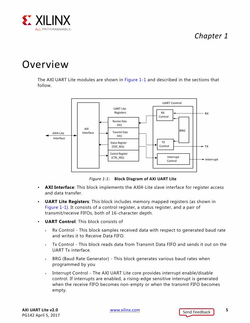
OverviewThe AXI UART Lite modules are shown in Figure 1-1 and described in the sections that follow.
• AXI Interface: This block implements the AXI4-Lite slave interface for register access and data transfer.
• UART Lite Registers: This block includes memory mapped registers (as shown in Figure 1-1). It consists of a control register, a status register, and a pair of transmit/receive FIFOs, both of 16-character depth.
• UART Control: This block consists of
° Rx Control - This block samples received data with respect to generated baud rate and writes it to Receive Data FIFO.
° Tx Control - This block reads data from Transmit Data FIFO and sends it out on the UART Tx interface.
° BRG (Baud Rate Generator) - This block generates various baud rates when programmed by you
° Interrupt Control - The AXI UART Lite core provides interrupt enable/disable control. If interrupts are enabled, a rising-edge sensitive interrupt is generated when the receive FIFO becomes non-empty or when the transmit FIFO becomes empty.
X-Ref Target - Figure 1-1
Figure 1-1: Block Diagram of AXI UART Lite
AXI4-Lite Interface
AXIInterface
UART LiteRegisters
Receive DataFIFO
Transmit DataFIFO
Status Register(STAT_REG)
Control Register(CTRL_REG)
BRG
RXControl
TXControl
Interrupt Control
RX
TX
Interrupt
UART Control
Send Feedback

AXI UART Lite v2.0 www.xilinx.com 6PG142 April 5, 2017
Chapter 1: Overview
Feature SummaryThe AXI UART Lite has the following features:
• Performs parallel-to-serial conversion on characters received through the AXI4-Lite interface and serial-to-parallel conversion on characters received from a serial peripheral.
• Transmits and receives 8, 7, 6, or 5-bit characters, with one stop bit and with odd, even, or no parity bit. The AXI UART Lite can transmit and receive independently.
• Generates a rising-edge sensitive interrupt when the receive FIFO becomes non-empty or when the transmit FIFO becomes empty. This interrupt can be masked by using an interrupt enable/disable signal. The device contains a baud rate generator and independent 16-character deep transmit and receive FIFOs.
Licensing and Ordering InformationThis Xilinx® LogiCORE™ IP module is provided at no additional cost with the Xilinx Vivado® Design Suite under the terms of the Xilinx End User License.
Information about this and other Xilinx LogiCORE IP modules is available at the Xilinx Intellectual Property page. For information on pricing and availability of other Xilinx LogiCORE IP modules and tools, contact your local Xilinx sales representative.
Send Feedback
AXI UART Lite v2.0 www.xilinx.com 7PG142 April 5, 2017
Chapter 2
Product Specification
PerformanceThe AXI UART Lite core is characterized as per the benchmarking methodology described in the Vivado Design Suite User Guide: Designing with IP (UG896) [Ref 6]. Table 2-1 shows the results of the characterization runs. Maximum frequencies achieved for various devices and speed grades based on the FMAX margin system are also shown in Table 2-1.
Note: Frequency data for UltraScale architecture-based devices and Zynq®-7000 devices are expected to be similar to 7 series device numbers.
Table 2-1: Maximum Frequencies
Family Speed Grade FMAX (MHz) for AXI4-Lite
Virtex-7
-1
180
Kintex-7 180
Artix-7 120
Virtex-7
-2
200
Kintex-7 200
Artix-7 140
Virtex-7
-3
220
Kintex-7 220
Artix-7 160
Send Feedback

AXI UART Lite v2.0 www.xilinx.com 8PG142 April 5, 2017
Chapter 2: Product Specification
Resource UtilizationThe AXI UART Lite resource utilization for various parameter combinations measured with a 7 series device.
Note: Resource numbers for UltraScale architecture-based devices and Zynq devices are expected to be similar to 7 series device numbers.
Port DescriptionsThe AXI UART Lite I/O signals are listed and described in Table 2-3.
Table 2-2: Device Utilization
Parameter Values (other parameters at default value) Device Resources
Baud
Rat
e
Data
Bits
Parit
y
Slic
es
Slic
eFl
ip-F
lops
LUTs
19200 5 0 41 77 100
19200 6 0 46 84 110
19200 7 1 59 84 114
9600 8 0 49 79 119
38400 8 0 44 77 107
19200 6 0 46 84 110
19200 7 1 59 84 114
Table 2-3: I/O Signal Descriptions
Signal Name Interface I/O Initial State Description
System Signals
s_axi_aclk System I - AXI clock.
s_axi_aresetn System I - AXI reset, active-Low.
interrupt System O O Edge rising UART interrupt.
AXI Channel Signals
s_axi_* S_AXI - -See the AXI Reference Guide (UG761) [Ref 4] for a description of AXI4 Signals.
UART Lite Interface Signals
Send Feedback

AXI UART Lite v2.0 www.xilinx.com 9PG142 April 5, 2017
Chapter 2: Product Specification
Register SpaceTable 2-4 shows all the AXI UART Lite registers and their addresses.
Note: The AXI4-Lite write access register is updated by the 32-bit AXI Write Data (*_wdata) signal, and is not impacted by the AXI Write Data Strobe (*_wstrb) signal. For write access, both the AXI Write Address Valid (*_awvalid) and AXI Write Data Valid (*_wvalid) signals should be asserted together.
RX FIFOThis 16-entry-deep FIFO contains data received by the AXI UART Lite core. The FIFO bit definitions are shown in Table 2-5. When a read request is issued to an empty FIFO, a bus error (SLVERR) is generated and the result is undefined. The RX FIFO is a read-only register. Issuing a write request to this register has no effect. Figure 2-1 shows the location for data on the AXI interface when Data Bits is set to 8 in the XGUI.
rx UART Lite I - Receive data
tx UART Lite O 0x1 Transmit data1. The AXI UART Lite core generates SLVERR when one of the following conditions is true:
° A read request is issued to an empty receive data FIFO.
° A write request is issued when the transmit data FIFO is full.For all other requests, OKAY response is passed. The AXI UART Lite never generates DECERR.
Table 2-4: Register Address Map
Address Offset Register Name Description
0h Rx FIFO Receive data FIFO
04h Tx FIFO Transmit data FIFO
08h STAT_REG UART Lite status register
0Ch CTRL_REG UART Lite control register
X-Ref Target - Figure 2-1
Figure 2-1: Rx FIFO (Data Bits = 8)
Table 2-3: I/O Signal Descriptions (Cont’d)
Signal Name Interface I/O Initial State Description
31 8 7 0
Rx Data
Reserved
Send Feedback
AXI UART Lite v2.0 www.xilinx.com 10PG142 April 5, 2017
Chapter 2: Product Specification
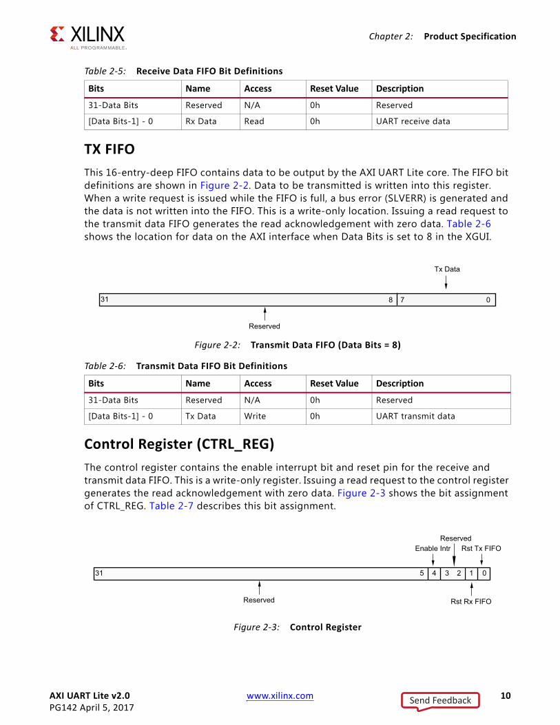
TX FIFOThis 16-entry-deep FIFO contains data to be output by the AXI UART Lite core. The FIFO bit definitions are shown in Figure 2-2. Data to be transmitted is written into this register. When a write request is issued while the FIFO is full, a bus error (SLVERR) is generated and the data is not written into the FIFO. This is a write-only location. Issuing a read request to the transmit data FIFO generates the read acknowledgement with zero data. Table 2-6 shows the location for data on the AXI interface when Data Bits is set to 8 in the XGUI.
Control Register (CTRL_REG)The control register contains the enable interrupt bit and reset pin for the receive and transmit data FIFO. This is a write-only register. Issuing a read request to the control register generates the read acknowledgement with zero data. Figure 2-3 shows the bit assignment of CTRL_REG. Table 2-7 describes this bit assignment.
Table 2-5: Receive Data FIFO Bit Definitions
Bits Name Access Reset Value Description
31-Data Bits Reserved N/A 0h Reserved
[Data Bits-1] - 0 Rx Data Read 0h UART receive data
X-Ref Target - Figure 2-2
Figure 2-2: Transmit Data FIFO (Data Bits = 8)
Table 2-6: Transmit Data FIFO Bit Definitions
Bits Name Access Reset Value Description
31-Data Bits Reserved N/A 0h Reserved
[Data Bits-1] - 0 Tx Data Write 0h UART transmit data
X-Ref Target - Figure 2-3
Figure 2-3: Control Register
31 8 7 0
Reserved
Tx Data
31 5 4 3 2 01
Rst Rx FIFO
Rst Tx FIFOReserved
Reserved
Enable Intr
Send Feedback

AXI UART Lite v2.0 www.xilinx.com 11PG142 April 5, 2017
Chapter 2: Product Specification
Status Register (STAT_REG)The status register contains the status of the receive and transmit data FIFOs when interrupts are enabled and errors are present. This is a read-only register. A write to this register has no effect. Bit assignment in the STAT_REG is shown in Figure 2-4 and described in Table 2-8.
Table 2-7: Control Register Bit Definitions
Bits Name Access Reset Value Description
31–5 Reserved N/A 0h Reserved
4 Enable Intr Write 0hEnable interrupt for the AXI UART Lite0 = Disable interrupt signal1 = Enable interrupt signal
3–2 Reserved N/A 0h Reserved
1 Rst Rx FIFO Write 0h
Reset/clear the receive FIFOWriting a 1 to this bit position clears the receive FIFO0 = Do nothing1 = Clear the receive FIFO
0 Rst Tx FIFO Write 0h
Reset/clear the transmit FIFOWriting a 1 to this bit position clears the transmit FIFO0 = Do nothing1 = Clear the transmit FIFO
X-Ref Target - Figure 2-4
Figure 2-4: Status Register
31 5 4 3 2 01
Rx FIFO Full
Tx FIFO Empty
Tx FIFO Full
Rx FIFO Valid Data
Reserved
6 7 8
Frame Error
Parity Error
OverrunError
Intr Enabled
Send Feedback

AXI UART Lite v2.0 www.xilinx.com 12PG142 April 5, 2017
Chapter 2: Product Specification
Table 2-8: Status Register Bit Definitions
Bits Name Access Reset Value Description
31 - 8 Reserved N/A 0h Reserved
7 Parity Error Read 0h
Indicates that a parity error has occurred after the last time the status register was read. If the UART is configured without any parity handling, this bit is always 0.The received character is written into the receive FIFO.This bit is cleared when the status register is read.0 = No parity error has occurred1 = Parity error has occurred
6 Frame Error Read 0h
Indicates that a frame error has occurred after the last time the status register was read. Frame error is defined as detection of a stop bit with the value 0. The receive character is ignored and not written to the receive FIFO.This bit is cleared when the status register is read.0 = No frame error has occurred1 = Frame error has occurred
5 Overrun Error Read 0h
Indicates that a overrun error has occurred after the last time the status register was read. Overrun is when a new character has been received but the receive FIFO is full. The received character is ignored and not written into the receive FIFO. This bit is cleared when the status register is read.0 = No overrun error has occurred1 = Overrun error has occurred
4 Intr Enabled Read 0h
Indicates that interrupts is enabled.0 = Interrupt is disabled1 = Interrupt is enabled
3 Tx FIFO Full Read 0hIndicates if the transmit FIFO is full.0 = Transmit FIFO is not full1 = Transmit FIFO is full
2 Tx FIFO Empty Read 01hIndicates if the transmit FIFO is empty.0 = Transmit FIFO is not empty1 = Transmit FIFO is empty
1 Rx FIFO Full Read 0h
Indicates if the receive FIFO is full.0 = Receive FIFO is not full1 = Receive FIFO is full
0 Rx FIFO Valid Data Read 0hIndicates if the receive FIFO has data.0 = Receive FIFO is empty1 = Receive FIFO has data
Send Feedback

AXI UART Lite v2.0 www.xilinx.com 13PG142 April 5, 2017
Chapter 3
Designing with the CoreThis chapter includes guidelines and additional information to facilitate designing with the core.
ClockingThe AXI UART Lite core operates on s_axi_aclk.
ResetsThe AXI UART Lite core resets when the s_axi_aresetn signal is asserted. This is an active-Low reset synchronous to s_axi_aclk.
Programming SequenceProgram CTRL_REG to enable interrupt if required. Data can be sent over the UART interface by writing to the TX FIFO. Similarly, UART data can be read by reading the RX FIFO when it is not empty.
Send Feedback

AXI UART Lite v2.0 www.xilinx.com 14PG142 April 5, 2017
Chapter 4
Design Flow StepsThis chapter describes customizing and generating the core, constraining the core, and the simulation, synthesis and implementation steps that are specific to this IP core. More detailed information about the standard Vivado® design flows and the IP integrator can be found in the following Vivado Design Suite user guides:
• Vivado Design Suite User Guide: Designing IP Subsystems using IP Integrator (UG994) [Ref 5]
• Vivado Design Suite User Guide: Designing with IP (UG896) [Ref 6]
• Vivado Design Suite User Guide: Getting Started (UG910) [Ref 7]
• Vivado Design Suite User Guide: Logic Simulation (UG900) [Ref 9]
Customizing and Generating the CoreThis chapter includes information about using Xilinx tools to customize and generate the core in the Vivado Design Suite.
Vivado Integrated Design EnvironmentYou can customize the IP for use in your design by specifying values for the various parameters associated with the IP core using the following steps:
1. Select the IP from the IP catalog.
2. Double-click the selected IP or select the Customize IP command from the toolbar or right-click menu .
For details, the Vivado Design Suite User Guide: Designing with IP (UG896) [Ref 6] and the Vivado Design Suite User Guide: Getting Started (UG910) [Ref 7].
Note: Figures in this chapter are illustrations of the Vivado Integrated Design Environment (IDE). This layout might vary from the current version.
If you are customizing and generating the core in the Vivado IP Integrator, see the Vivado Design Suite User Guide: Designing IP Subsystems using IP Integrator (UG994) [Ref 5] for detailed information. IP Integrator might auto-compute certain configuration values when validating or generating the design. To check whether the values do change, see the
Send Feedback

AXI UART Lite v2.0 www.xilinx.com 15PG142 April 5, 2017
Chapter 4: Design Flow Steps
description of the parameter in this chapter. To view the parameter value you can run the validate_bd_design command in the tcl console.
• AXI CLK Frequency. System clock frequency (in MHz) driving the AXI UART Lite peripheral.
Note: The AXI CLK Frequency parameter is pre-determined when using IP Integrator.
• Baud Rate. Baud rate of the AXI UART Lite core in bits per second. The core supports the following rates:
Note: The GUI factors in the tolerance allows only valid baud rate values to be set, based on the AXI clock frequency.
X-Ref Target - Figure 4-1
Figure 4-1: Vivado IDE
110 2400 19,200 115,200 460,800
300 4800 38,400 128,000 921,600
1200 9600 57,600 230,400
Send Feedback

AXI UART Lite v2.0 www.xilinx.com 16PG142 April 5, 2017
Chapter 4: Design Flow Steps
• Data Bits. The number of data bits in the serial frame. The core supports bits 5, 6, 7, and 8.
• Parity. Determines whether parity is used or not. If used whether parity is odd or even.
Output GenerationFor details, see the Vivado Design Suite User Guide: Designing with IP (UG896) [Ref 6].
Constraining the CoreSince this core has external pins, it is recommended that you add the required input/output delay constraints, based on the board delays.
An example of such constraints is as follows:
set_input_delay -clock clk_port -max 2 [get_ports rs232_uart_rxd]set_input_delay -clock clk_port -min 1 [get_ports rs232_uart_rxd]set_output_delay -clock clk_port -max 2 [get_ports rs232_uart_txd]set_output_delay -clock clk_port -min 1 [get_ports rs232_uart_txd]
The minimum and maximum values are to be determined based on the board delays.
Required ConstraintsThis section is not applicable for this IP core.
Device, Package, and Speed Grade SelectionsThis section is not applicable for this IP core.
Clock FrequenciesThis section is not applicable for this IP core.
Clock ManagementThis section is not applicable for this IP core.
Clock PlacementThis section is not applicable for this IP core.
Send Feedback

AXI UART Lite v2.0 www.xilinx.com 17PG142 April 5, 2017
Chapter 4: Design Flow Steps
BankingThis section is not applicable for this IP core.
Transceiver PlacementThis section is not applicable for this IP core.
I/O Standard and PlacementThis section is not applicable for this IP core.
SimulationFor simulation details, see the Vivado Design Suite User Guide: Logic Simulation (UG900) [Ref 7].
Synthesis and ImplementationFor details about synthesis and implementation, see the Vivado Design Suite User Guide: Designing with IP (UG896) [Ref 6].
Send Feedback

AXI UART Lite v2.0 www.xilinx.com 18PG142 April 5, 2017
Chapter 5
Example DesignThis chapter contains information about the example design provided in the Vivado® Design Suite.
OverviewThe top module instantiates all components of the core and example design that are needed to implement the design in hardware, as shown in Figure 5-1. This includes the clock generator (MMCME2), register configuration, data generator and data checker modules.
This example design includes two modules:
• Clock Generator: MMCME2 is used to generate the clocks for the example design. MMCME2 is used to generate the 100 MHz clock for s_axi_aclk. The DUT and other modules of the example design are kept under reset until MMCME2 is locked.
X-Ref Target - Figure 5-1
Figure 5-1: Example Design Block Diagram
AXI Traffic Generator
DUT
Clock Generator
<Componentname>_exdes.vhd (top)
AXI4Lite
clock_in
resetclock_gen.vhd
tx
X13606
rx
done
status
Send Feedback

AXI UART Lite v2.0 www.xilinx.com 19PG142 April 5, 2017
Chapter 5: Example Design
• AXI Traffic Generator (ATG): This module is configured in System Test mode. All the AXI UART Lite-related AXI4-Lite transactions are stored in the COE/MIF file. For more information on the AXI Traffic Generator, see the AXI Traffic Generator Product Guide (PG125) [Ref 8]. The ATG automatically starts the AXI4-Lite transaction after coming out of reset.
Implementing the Example DesignAfter following the steps described in Chapter 4, Customizing and Generating the Core, implement the example design as follows:
1. Right-click the core in the Hierarchy window, and select Open IP Example Design.
2. A new window pops up, asking you to specify a directory for the example design. Select a new directory, or keep the default directory.
3. A new project is automatically created in the selected directory and opened in a new Vivado window.
4. In the Flow Navigator (left side pane), click Run Implementation and follow the directions.
The ATG writes 0x41 to tx_fifo of AXI UART Lite. The serial port of the KC705 board should be connected to your PC. You can open the serial port terminal to check if the character "A" is displayed or not. Upon successful ATG transactions, the character "A" is displayed in the serial port terminal. If there is an error, the character "A" is not displayed.
Example Design Directory StructureIn the current project directory, a new project with name <component_name>_example is created and the files are delivered to <component_name>_example/<component_name>_example.srcs. This directory and its subdirectories contain all the source files required to create the AXI UART Lite controller example design.
Table 5-1 lists the files delivered in <component_name>_example/<component_name>_example.srcs/sources_1/imports/example_design.
Table 5-1: Example Design Directory
Name Description
<component_name>_exdes.vhd Top-level HDL file for the example design.
clock_gen.vhd Clock generation module for example design.
atg_addr.coe COE file of address. This file contains the AXI UART Lite register address.
Send Feedback

AXI UART Lite v2.0 www.xilinx.com 20PG142 April 5, 2017
Chapter 5: Example Design
The <component_name>_example/<component_name>_example.srcs/sources_1/sim_1/imports/simulation directory contains the test bench file for the example design: <component_name>_exdes_tb.vhd.
The <component_name>_example/<component_name>_example.srcs/sources_1/constrs_1/imports/example_design directory contains the top-level constraints file for the example design: <component_name>_exdes.xdc.
The XDC has all the necessary constraints needed to run the example design on the KC705 board. All the IO constraints are commented in the XDC file. Please uncomment these constraints before implementing the design on the KC705 board.
Simulating the Example DesignThe AXI UART Lite example design simulates and demonstrates the behavior of the AXI Timer.
Simulation ResultsThe simulation script compiles the AXI Timer example design, and supporting simulation files. It then runs the simulation and checks to ensure that it completed successfully.
If test passes, the following message is displayed:
Test Completed Successfully
If the test fails or does not complete, the following message is displayed:
Test Failed !! Test Timed Out
atg_data.coe COE file of data. This file contains the data to be written/read from the AXI UART Lite registers.
atg_mask.coe COE file to mask certain reads.
atg_ctrl.coe COE file that contains control information of ATG.
Table 5-1: Example Design Directory (Cont’d)
Name Description
Send Feedback

AXI UART Lite v2.0 www.xilinx.com 21PG142 April 5, 2017
Chapter 6
Test BenchThis chapter contains information about the test bench provided in the Vivado® Design Suite.
Figure 6-1 shows the test bench for AXI UART Lite example design. The top-level test bench generates 200 MHz clock and drives initial reset to the example design. As shown in the diagram, test status consists of a baud rate generator and a serial-to-parallel shift register. The baud rate is automatically calculated by the user parameters inputs. When complete, a byte of data is transmitted into the shift register. The test status then checks for ASCI character "A".
X-Ref Target - Figure 6-1
Figure 6-1: Test Bench Block Diagram
Clock & reset generation
<componentname>_exdes.vhd(top)
Test Status
clock_in
reset
top_tb
tx
X13607
Send Feedback

AXI UART Lite v2.0 www.xilinx.com 22PG142 April 5, 2017
Appendix A
Migrating and UpgradingThis appendix contains information about migrating a design from the ISE® Design Suite to the Vivado® Design Suite, and for upgrading to a more recent version of the IP core. For customers upgrading in the Vivado Design Suite, important details (where applicable) about any port changes and other impact to user logic are included.
Migrating to the Vivado Design SuiteFor information about migrating to the Vivado Design Suite, see the ISE to Vivado Design Suite Migration Guide (UG911) [Ref 10].
Upgrading in the Vivado Design SuiteThis section provides information about any changes to the user logic or port designations that take place when you upgrade to a more current version of this IP core in the Vivado Design Suite.
Parameter Changes There are no parameter changes.
Port ChangesThere are no port changes.
Send Feedback

AXI UART Lite v2.0 www.xilinx.com 23PG142 April 5, 2017
Appendix B
DebuggingThis appendix includes details about resources available on the Xilinx® Support website.
Finding Help on Xilinx.comTo help in the design and debug process when using the AXI UART Lite, the Xilinx Support web page (Xilinx Support web page) contains key resources such as product documentation, release notes, answer records, information about known issues, and links for obtaining further product support.
DocumentationThis product guide is the main document associated with the AXI UART Lite. This guide, along with documentation related to all products that aid in the design process, can be found on the Xilinx Support web page or by using the Xilinx Documentation Navigator.
Download the Xilinx Documentation Navigator from the Downloads page. For more information about this tool and the features available, open the online help after installation.
Answer RecordsAnswer Records include information about commonly encountered problems, helpful information on how to resolve these problems, and any known issues with a Xilinx product. Answer Records are created and maintained daily ensuring that users have access to the most accurate information available.
Answer Records for this core can be located by using the Search Support box on the main Xilinx support web page. To maximize your search results, use proper keywords such as
• Product name
• Tool message(s)
• Summary of the issue encountered
A filter search is available after results are returned to further target the results.
Send Feedback

AXI UART Lite v2.0 www.xilinx.com 24PG142 April 5, 2017
Appendix B: Debugging
Master Answer Record for the AXI UART Lite
AR: 54421
Technical SupportXilinx provides technical support in the Xilinx Support web page for this LogiCORE™ IP product when used as described in the product documentation. Xilinx cannot guarantee timing, functionality, or support if you do any of the following:
• Implement the solution in devices that are not defined in the documentation.
• Customize the solution beyond that allowed in the product documentation.
• Change any section of the design labeled DO NOT MODIFY.
To contact Xilinx Technical Support, navigate to the Xilinx Support web page.
Vivado Design Suite Debug FeatureThe Vivado® Design Suite debug feature inserts logic analyzer and virtual I/O cores directly into your design. The debug feature also allows you to set trigger conditions to capture application and integrated block port signals in hardware. Captured signals can then be analyzed. This feature in the Vivado IDE is used for logic debugging and validation of a design running in Xilinx FPGA devices.
The Vivado logic analyzer is used to interact with the logic debug LogiCORE IP cores, including:
• ILA 2.0 (and later versions)
• VIO 2.0 (and later versions)
Hardware DebugHardware issues can range from link bring-up to problems seen after hours of testing. This section provides debug steps for common issues. The Vivado lab tools are valuable resource to use in hardware debug. The signal names mentioned in the following individual sections can be probed using the Vivado lab tools for debugging the specific problems.
Send Feedback

AXI UART Lite v2.0 www.xilinx.com 25PG142 April 5, 2017
Appendix C
Additional Resources and Legal Notices
Xilinx ResourcesFor support resources such as Answers, Documentation, Downloads, and Forums, see Xilinx® Support.
ReferencesThese documents provide supplemental material useful with this product guide:
1. AMBA® AXI4-Stream Protocol Specification
2. LogiCORE IP AXI4-Lite IPIF (DS765)
3. 7 Series FPGAs Overview (DS180)
4. AXI Reference Guide (UG761)
5. Vivado® Design Suite User Guide: Designing IP Subsystems using IP Integrator (UG994)
6. Vivado Design Suite User Guide: Designing with IP (UG896)
7. Vivado Design Suite User Guide: Getting Started (UG910)
8. AXI Traffic Generator Product Guide (PG125)
9. Vivado Design Suite User Guide: Logic Simulation (UG900)
10. ISE® to Vivado Design Suite Migration Methodology Guide (UG911)
Send Feedback

AXI UART Lite v2.0 www.xilinx.com 26PG142 April 5, 2017
Appendix C: Additional Resources and Legal Notices
Revision HistoryThe following table shows the revision history for this document.
Please Read: Important Legal NoticesThe information disclosed to you hereunder (the "Materials") is provided solely for the selection and use of Xilinx products. To the maximum extent permitted by applicable law: (1) Materials are made available "AS IS" and with all faults, Xilinx hereby DISCLAIMS ALL WARRANTIES AND CONDITIONS, EXPRESS, IMPLIED, OR STATUTORY, INCLUDING BUT NOT LIMITED TO WARRANTIES OF MERCHANTABILITY, NON-INFRINGEMENT, OR FITNESS FOR ANY PARTICULAR PURPOSE; and (2) Xilinx shall not be liable (whether in contract or tort, including negligence, or under any other theory of liability) for any loss or damage of any kind or nature related to, arising under, or in connection with, the Materials (including your use of the Materials), including for any direct, indirect, special, incidental, or consequential loss or damage (including loss of data, profits, goodwill, or any type of loss or damage suffered as a result of any action brought by a third party) even if such damage or loss was reasonably foreseeable or Xilinx had been advised of the possibility of the same. Xilinx assumes no obligation to correct any errors contained in the Materials or to notify you of updates to the Materials or to product specifications. You may not reproduce, modify, distribute, or publicly display the Materials without prior written consent. Certain products are subject to the terms and conditions of Xilinx's limited warranty, please refer to Xilinx's Terms of Sale which can be viewed at https://www.xilinx.com/legal.htm#tos; IP cores may be subject to warranty and support terms contained in a license issued to you by Xilinx. Xilinx products are not designed or intended to be fail-safe or for use in any application requiring fail-safe performance; you assume sole risk and liability for use of Xilinx products in such critical applications, please refer to Xilinx's Terms of Sale which can be viewed at https://www.xilinx.com/legal.htm#tos.AUTOMOTIVE APPLICATIONS DISCLAIMERAUTOMOTIVE PRODUCTS (IDENTIFIED AS “XA” IN THE PART NUMBER) ARE NOT WARRANTED FOR USE IN THE DEPLOYMENT OF AIRBAGS OR FOR USE IN APPLICATIONS THAT AFFECT CONTROL OF A VEHICLE (“SAFETY APPLICATION”) UNLESS THERE IS A SAFETY CONCEPT OR REDUNDANCY FEATURE CONSISTENT WITH THE ISO 26262 AUTOMOTIVE SAFETY STANDARD (“SAFETY DESIGN”). CUSTOMER SHALL, PRIOR TO USING OR DISTRIBUTING ANY SYSTEMS THAT INCORPORATE PRODUCTS, THOROUGHLY TEST SUCH SYSTEMS FOR SAFETY PURPOSES. USE OF PRODUCTS IN A SAFETY APPLICATION WITHOUT A SAFETY DESIGN IS FULLY AT THE RISK OF CUSTOMER, SUBJECT ONLY TO APPLICABLE LAWS AND REGULATIONS GOVERNING LIMITATIONS ON PRODUCT LIABILITY.© Copyright 2013–2017 Xilinx, Inc. Xilinx, the Xilinx logo, Artix, ISE, Kintex, Spartan, Virtex, Vivado, Zynq, and other designated brands included herein are trademarks of Xilinx in the United States and other countries. AMBA, AMBA Designer, ARM, ARM1176JZ-S, CoreSight, Cortex, and PrimeCell are trademarks of ARM in the EU and other countries. All other trademarks are the property of their respective owners.
Date Version Revision
04/05/2017 2.0 • Added description about the constraints that may be needed.
10/05/2016 2.0 • Added a note in Register Space section under Chapter 2, Product Specification.
• Updated in Please Read: Important Legal Notices section
11/18/2015 2.0 Added support for UltraScale+ families.
04/02/2014 2.0 • Updated resources information.• Minor updates and corrections.
12/18/2013 2.0 • Added support for UltraScale Architecture.
10/02/2013 2.0 • Added the Example Design and Test Bench chapters. • Added the Migrating and Updating appendix.• Added support for IP Integrator.
03/20/2013 1.0 Initial release as a product guide. This document is derived from DS741.
Send Feedback


![LogiCORE IP AXI to APB Bridge v2 - XilinxThe 32-bit AXI4-Lite interface on the AXI to APB Bridge core is based on the AMBA AXI and ACE Protocol Specification v2.0 [Ref 1]. The core](https://static.documents.pub/doc/80x56/5ea76a1bf3eb741af75f6d89/logicore-ip-axi-to-apb-bridge-v2-xilinx-the-32-bit-axi4-lite-interface-on-the.jpg)


