30
21
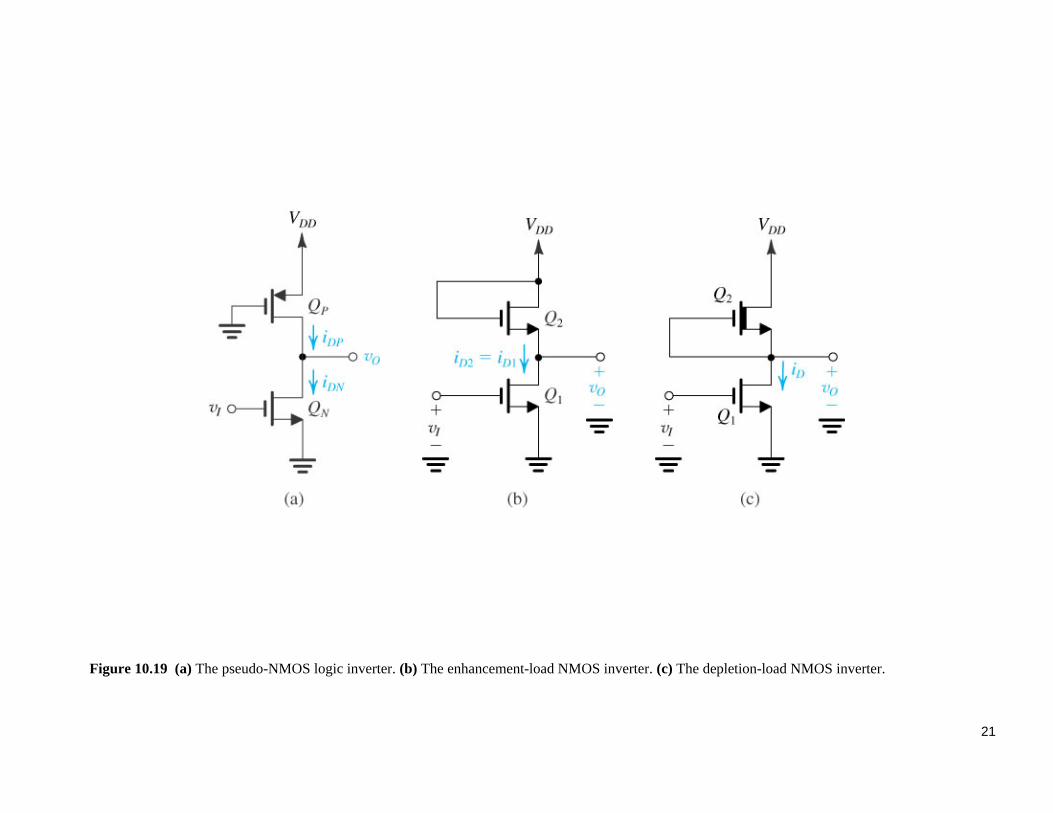
Figure 10.19 (a) The pseudo-NMOS logic inverter. (b) The enhancement-load NMOS inverter. (c) The depletion-load NMOS inverter.
22
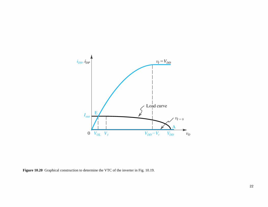
Figure 10.20 Graphical construction to determine the VTC of the inverter in Fig. 10.19.
23
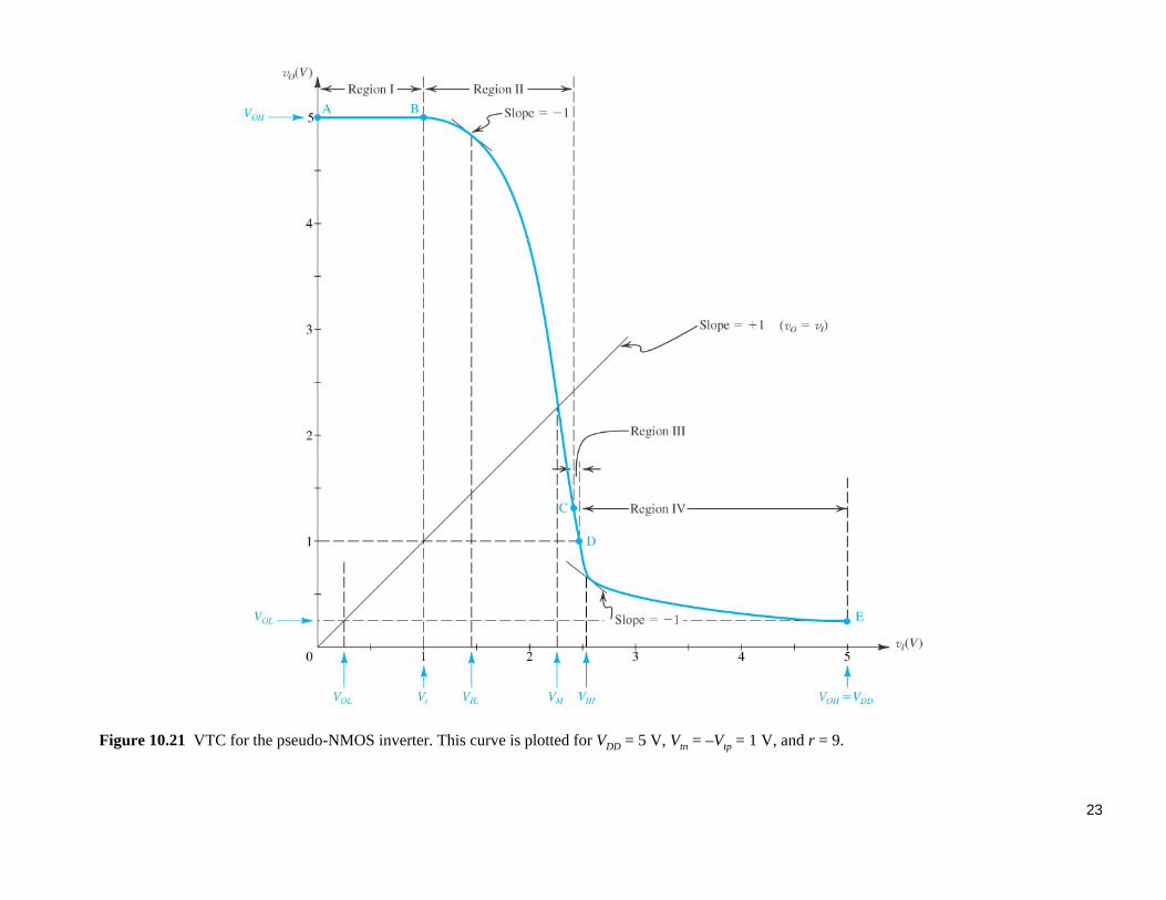
Figure 10.21 VTC for the pseudo-NMOS inverter. This curve is plotted for VDD = 5 V, Vtn = –Vtp = 1 V, and r = 9.
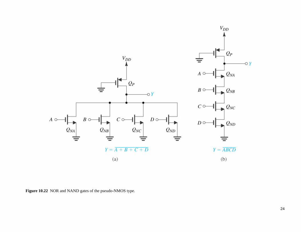
24
Figure 10.22 NOR and NAND gates of the pseudo-NMOS type.
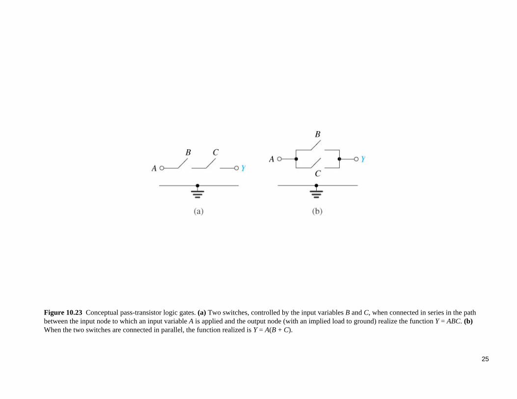
25
Figure 10.23 Conceptual pass-transistor logic gates. (a) Two switches, controlled by the input variables B and C, when connected in series in the path between the input node to which an input variable A is applied and the output node (with an implied load to ground) realize the function Y = ABC. (b)When the two switches are connected in parallel, the function realized is Y = A(B + C).
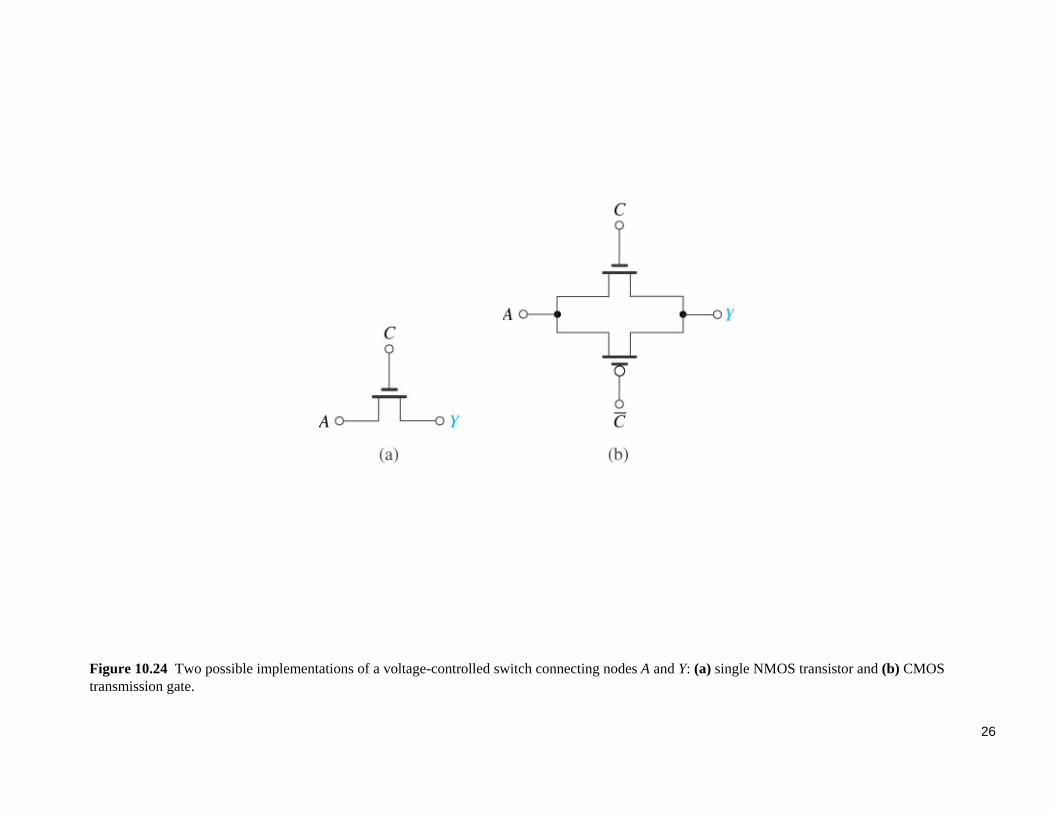
26
Figure 10.24 Two possible implementations of a voltage-controlled switch connecting nodes A and Y: (a) single NMOS transistor and (b) CMOS transmission gate.
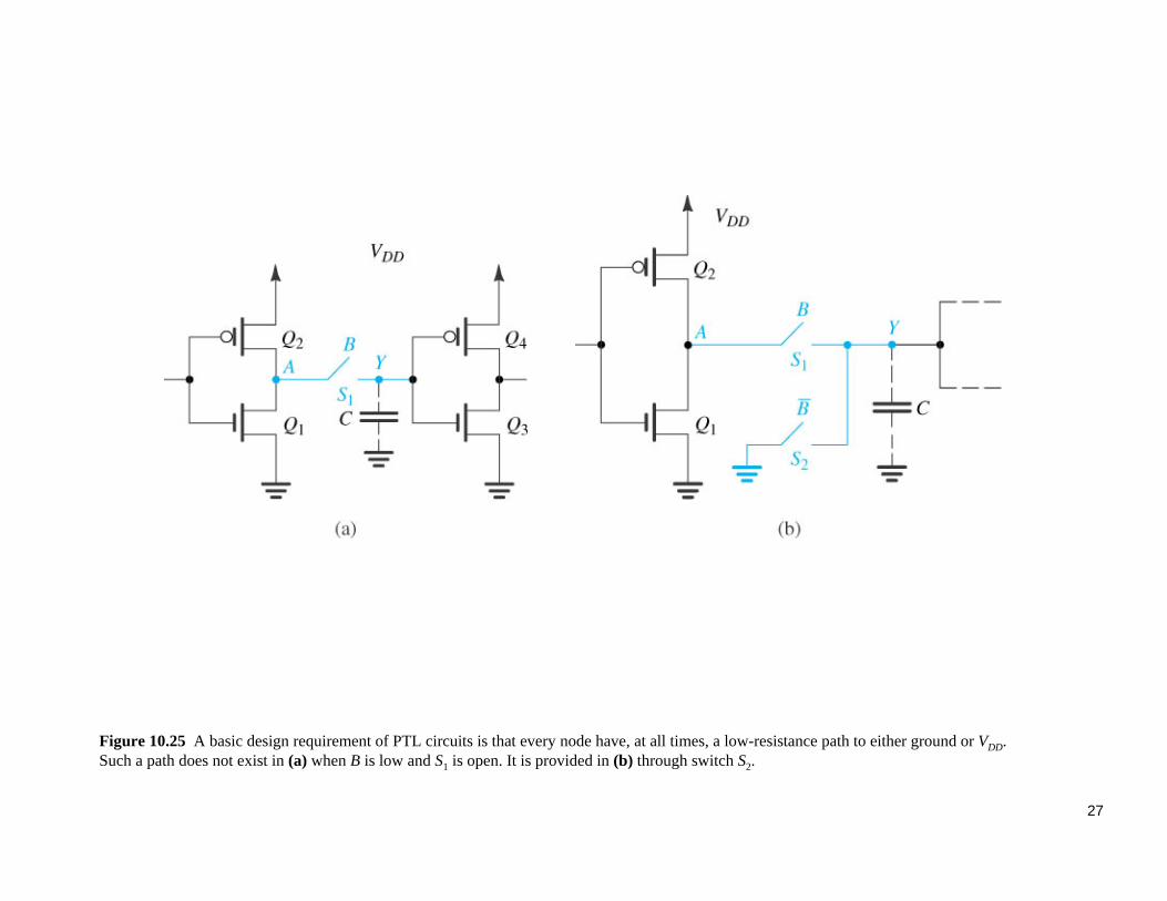
27
Figure 10.25 A basic design requirement of PTL circuits is that every node have, at all times, a low-resistance path to either ground or VDD. Such a path does not exist in (a) when B is low and S1 is open. It is provided in (b) through switch S2.
28
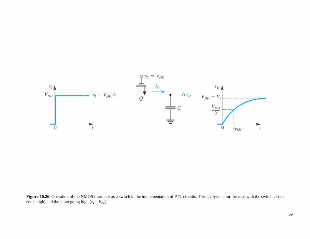
Figure 10.26 Operation of the NMOS transistor as a switch in the implementation of PTL circuits. This analysis is for the case with the switch closed (vC is high) and the input going high (vI = VDD).
29
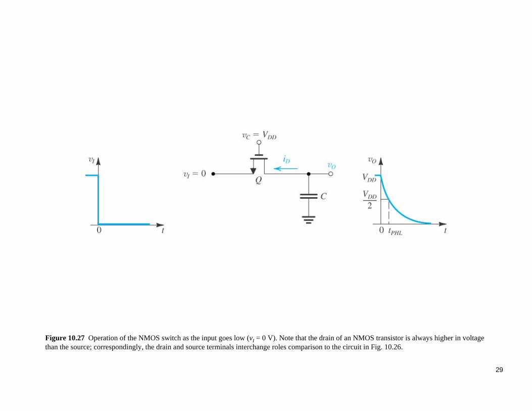
Figure 10.27 Operation of the NMOS switch as the input goes low (vI = 0 V). Note that the drain of an NMOS transistor is always higher in voltage than the source; correspondingly, the drain and source terminals interchange roles comparison to the circuit in Fig. 10.26.
30
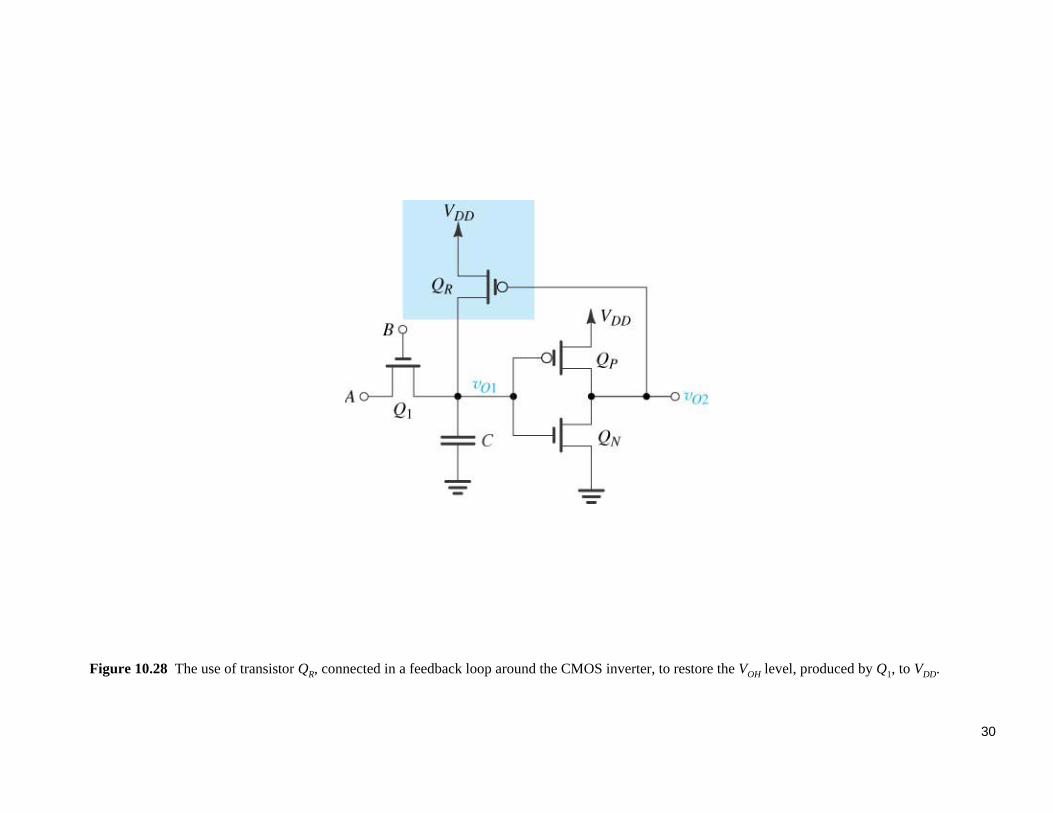
Figure 10.28 The use of transistor QR, connected in a feedback loop around the CMOS inverter, to restore the VOH level, produced by Q1, to VDD.
31
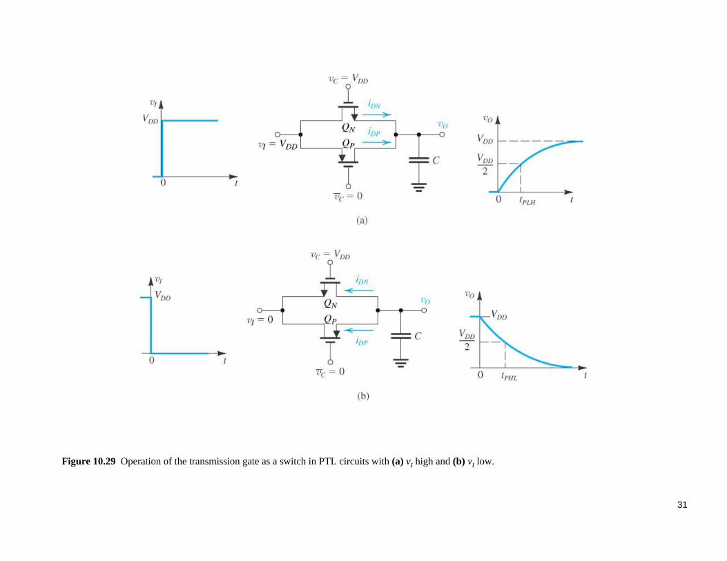
Figure 10.29 Operation of the transmission gate as a switch in PTL circuits with (a) vI high and (b) vI low.
32
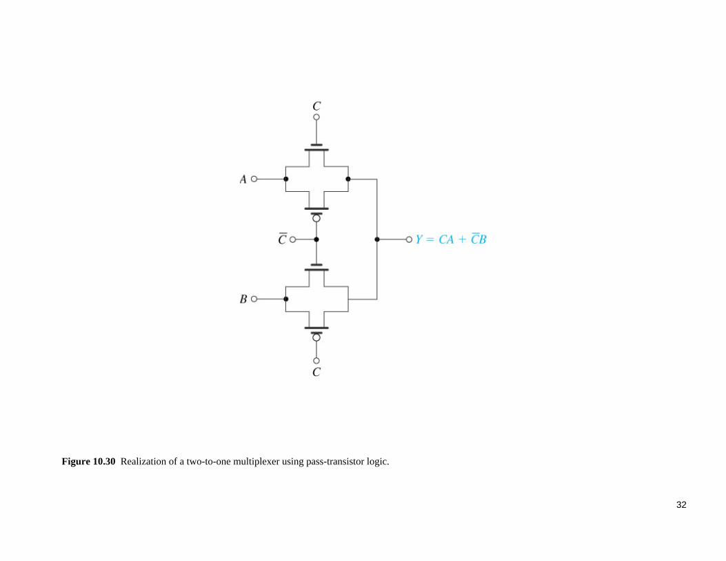
Figure 10.30 Realization of a two-to-one multiplexer using pass-transistor logic.
33
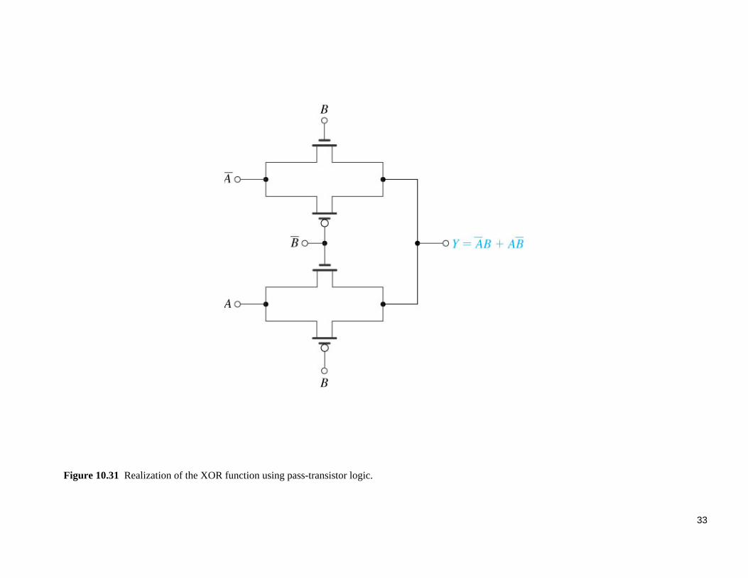
Figure 10.31 Realization of the XOR function using pass-transistor logic.
34
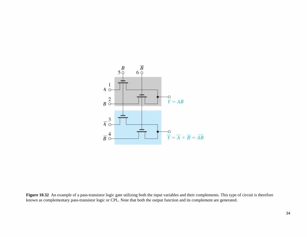
Figure 10.32 An example of a pass-transistor logic gate utilizing both the input variables and their complements. This type of circuit is therefore known as complementary pass-transistor logic or CPL. Note that both the output function and its complement are generated.
35
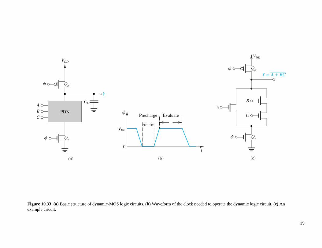
Figure 10.33 (a) Basic structure of dynamic-MOS logic circuits. (b) Waveform of the clock needed to operate the dynamic logic circuit. (c) An example circuit.
36
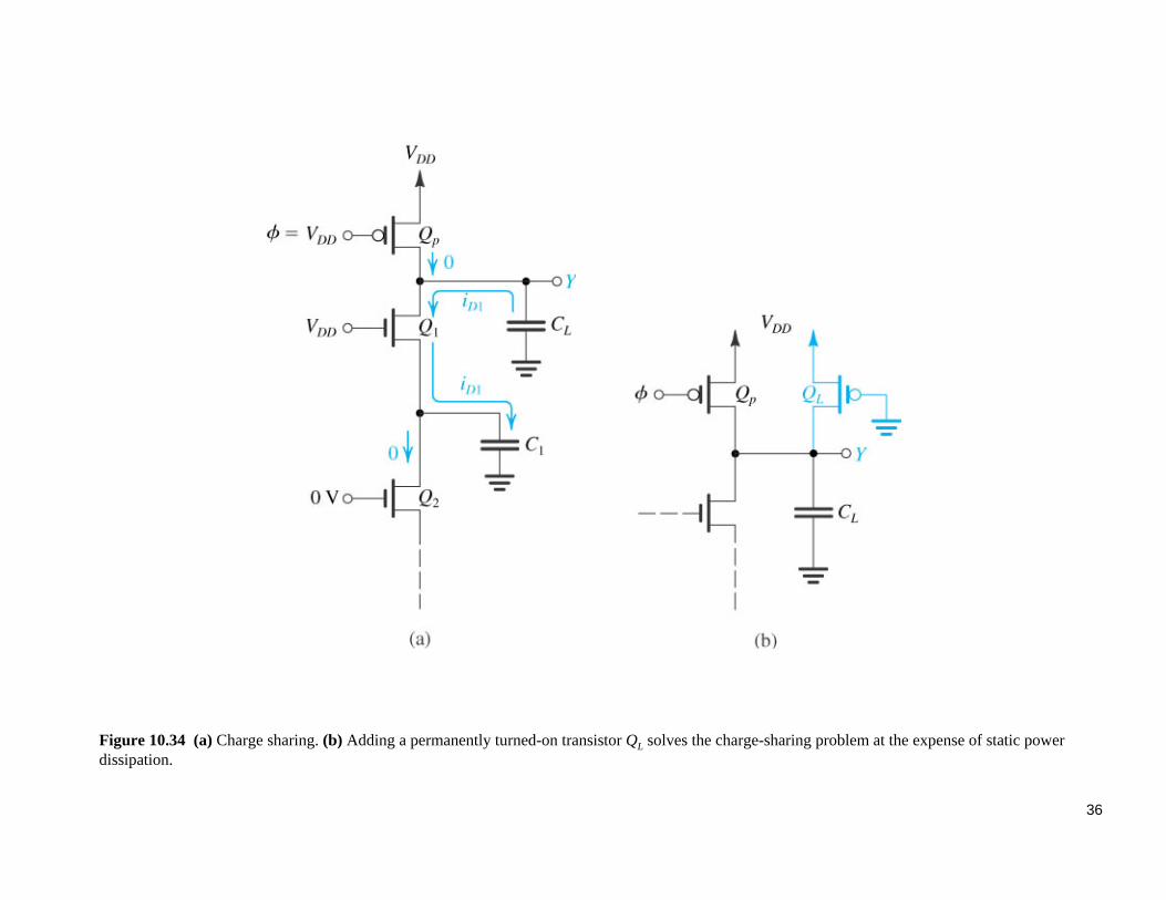
Figure 10.34 (a) Charge sharing. (b) Adding a permanently turned-on transistor QL solves the charge-sharing problem at the expense of static power dissipation.
37
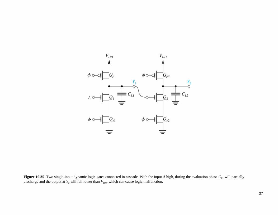
Figure 10.35 Two single-input dynamic logic gates connected in cascade. With the input A high, during the evaluation phase CL2 will partially discharge and the output at Y2 will fall lower than VDD, which can cause logic malfunction.
38
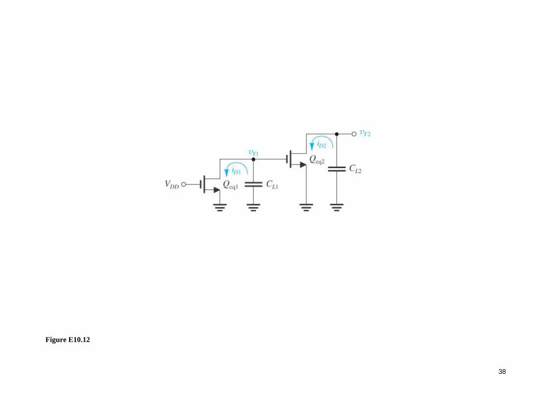
Figure E10.12
39
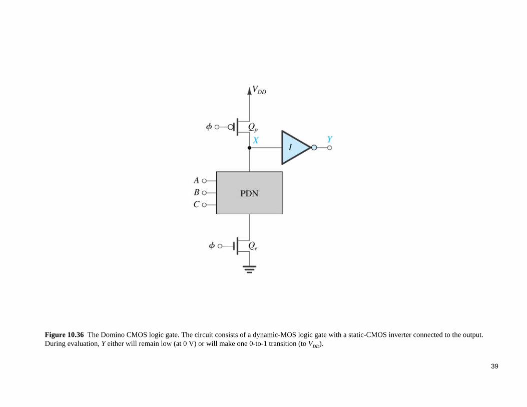
Figure 10.36 The Domino CMOS logic gate. The circuit consists of a dynamic-MOS logic gate with a static-CMOS inverter connected to the output. During evaluation, Y either will remain low (at 0 V) or will make one 0-to-1 transition (to VDD).
40
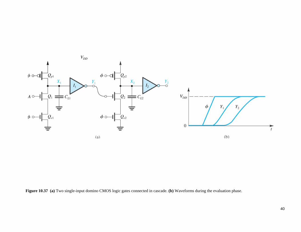
Figure 10.37 (a) Two single-input domino CMOS logic gates connected in cascade. (b) Waveforms during the evaluation phase.
41
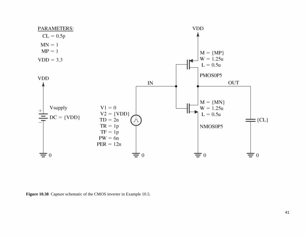
Figure 10.38 Capture schematic of the CMOS inverter in Example 10.5.
42
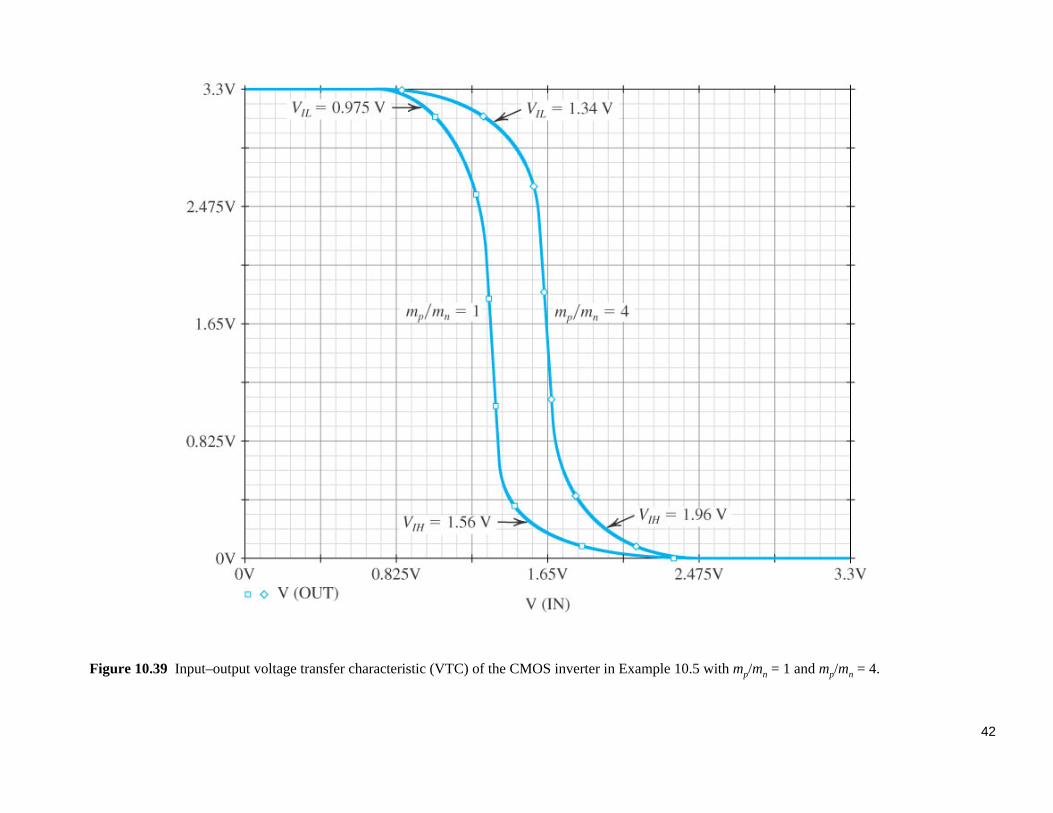
Figure 10.39 Input–output voltage transfer characteristic (VTC) of the CMOS inverter in Example 10.5 with mp/mn = 1 and mp/mn = 4.
43
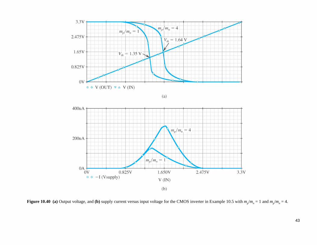
Figure 10.40 (a) Output voltage, and (b) supply current versus input voltage for the CMOS inverter in Example 10.5 with mp/mn = 1 and mp/mn = 4.
44
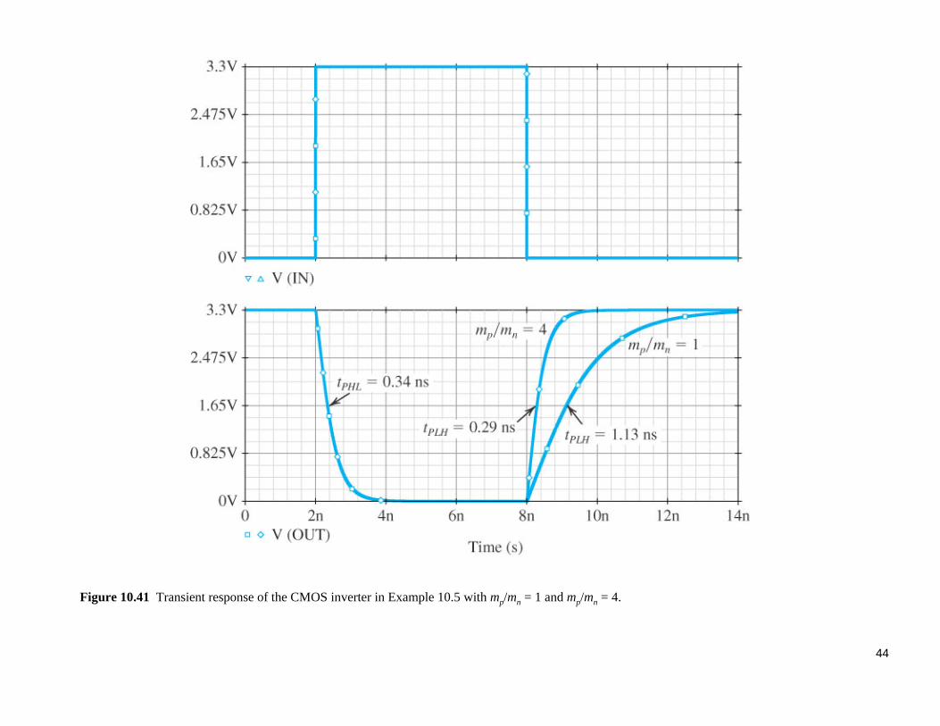
Figure 10.41 Transient response of the CMOS inverter in Example 10.5 with mp/mn = 1 and mp/mn = 4.
45
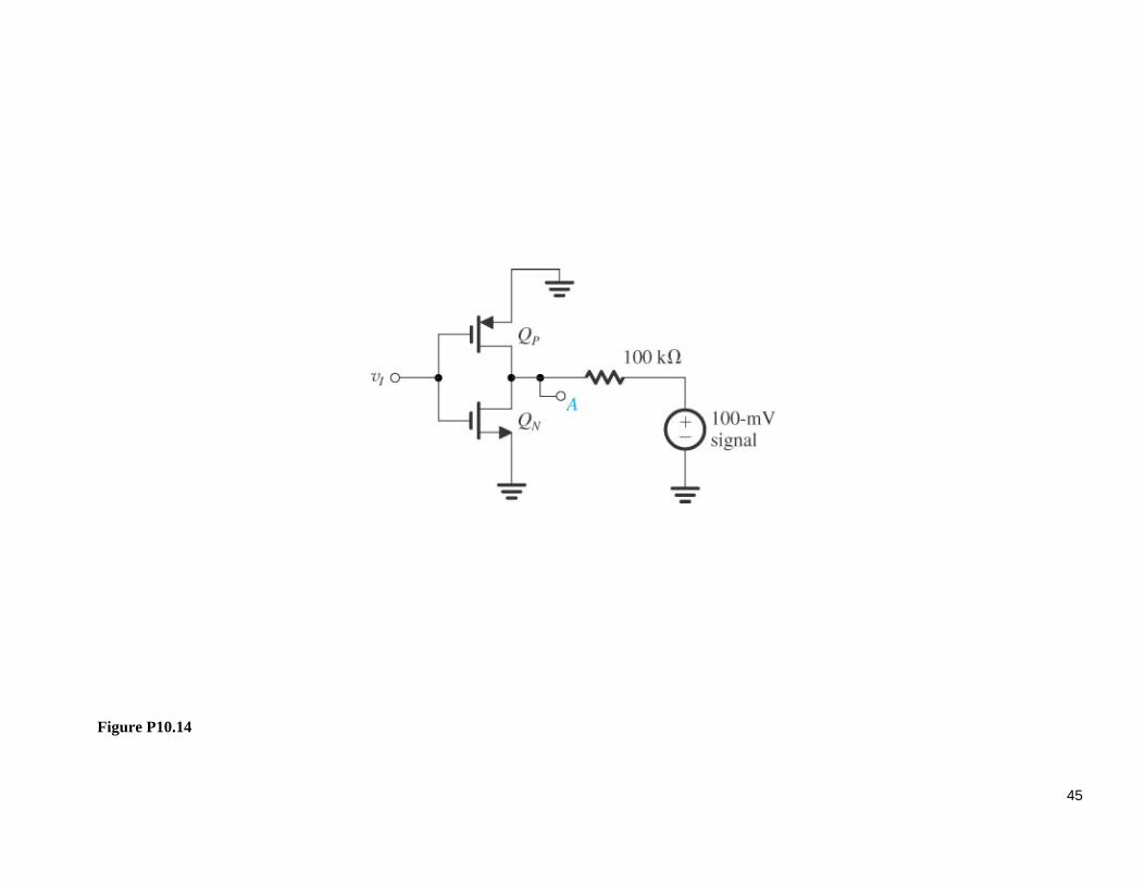
Figure P10.14
46
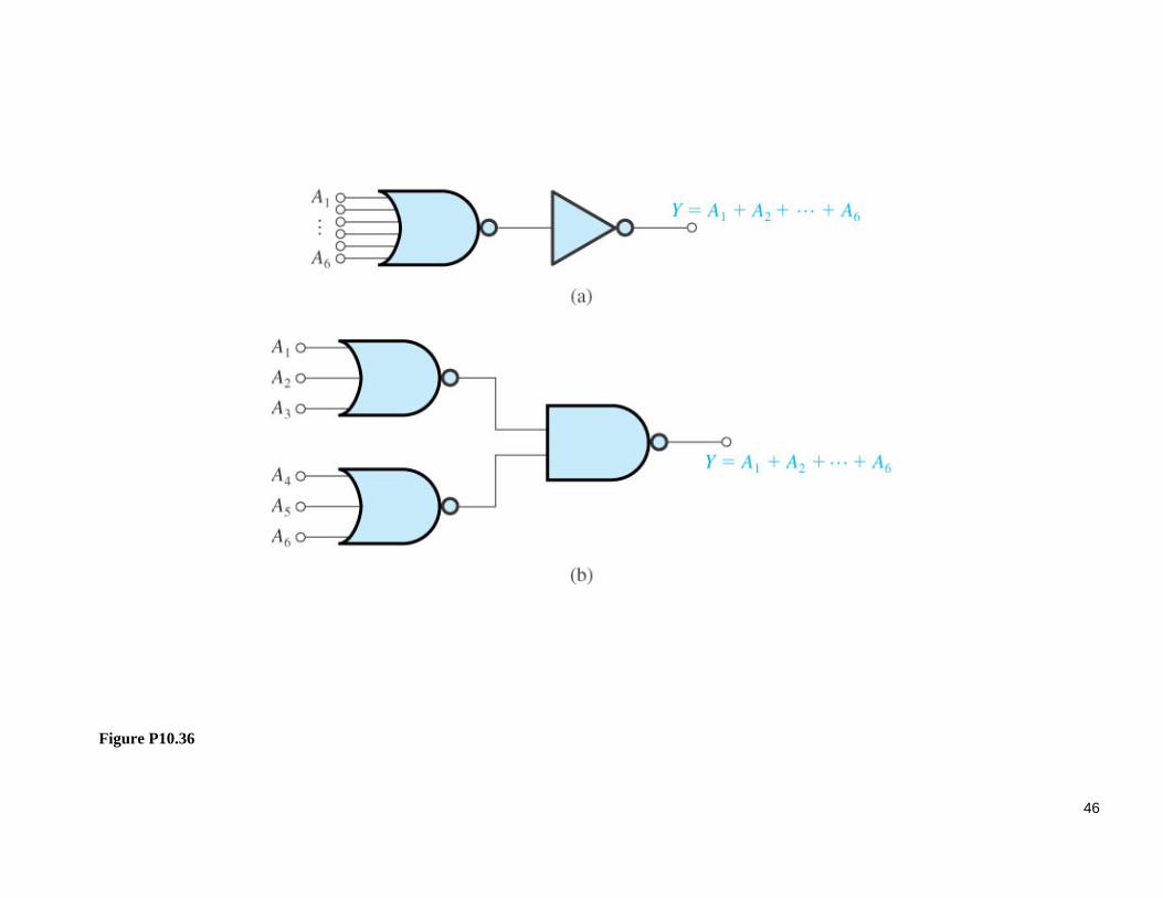
Figure P10.36
47
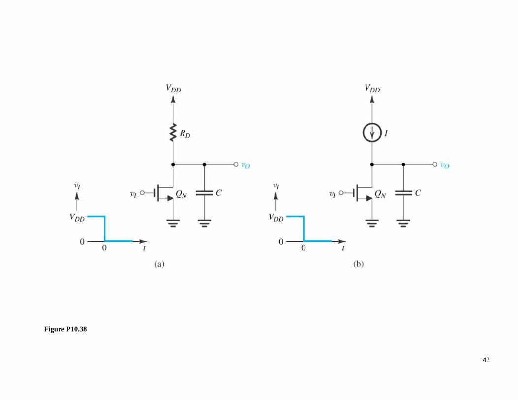
Figure P10.38
48
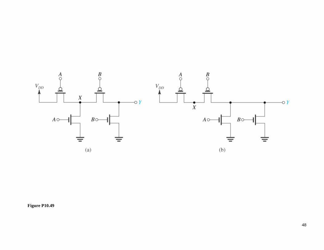
Figure P10.49
49
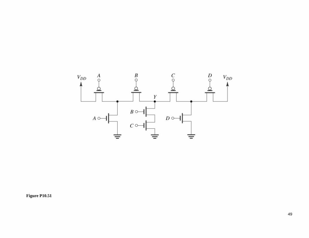
Figure P10.51