1 Department of Electronics Engineering, S.R. Group of Institutions,Jhansi, India
2 Department of Electronics Engineering, Bundelkhand University,Jhansi, India
3 Department of Electronics Engineering, Bundelkhand Institute of Engineering & Technology,Jhansi, India
4 Department of Electronics Engineering, Indian Institute of Information Technology,Allahabad, India
Received 19 January 2014; accepted 17 March 2014
Abstract: A novel compact broadband microstrip patch antenna is presented for various wireless applications. The pro-posed antenna has been fabricated and the impedance bandwidth and radiation pattern are measured. Thesimulated and measured antenna characteristics along with radiation pattern and gain are presented. It is statedthat the proposed designed antenna can completely cover the required band widths of Digital communicationsystem (DCS 1.71-1.88 GHz), Personal communication system (PCS 1.85-1.88 GHz) and IEEE 802.11b/g (2.4-2.485 GHz) with satisfactory radiation characteristics. The Experimental result shows that the proposed antennapresents a bandwidth 60.25% covering the range of 1.431- 2.665 GHz with the maximum radiation efficiency90%.
Microstrip antennas (MSAs) are gaining popularityamongst the researchers due to its attractive features suchas low profile, low cost, light weight, ease of fabricationand compatibility with microwave circuits[1, 2]. However,despite of these several advantages, the microstrip anten-∗E-mail: [email protected]
nas suffers from some disadvantages of narrow bandwidthand low efficiency. Various researches have been madeto increase the bandwidth of Microstrip antennas, whichincludes increase of the substrate thickness, the use of alow dielectric constant, slotted patch antennas, introduc-ing the parasitic elements either in coplanar or stackedconfiguration, the use of various impedance matching andfeeding techniques [3–8]. The dielectric constant of thesubstrate is closely related to the size and the bandwidthof the microstrip antenna. Low dielectric constant of thesubstrate produces larger bandwidth, while the high di-281
Bandwidth optimization of compact microstrip antenna for PCS/DCS/bluetooth application
electric constant of the substrate results in smaller size ofantenna [12–15]. A trade-off relationship exists betweenantenna size and bandwidth.In the past few years researchers have tried various meth-ods to enhance the bandwidth and it is observed that asthe bandwidth is increased the efficiency and gain de-creases. To obtain a larger bandwidth along with optimumgain and efficiency and maintaining the size of antenna isa major challenge to the researchers working with mi-crostrip antennas these days. In the past decade manyplanar antenna had been designed to meet the require-ment of mobile cellular communication systems. The mostdemanding these days are Global system for mobile com-munication system (GSM) ranging from 890 MHz to 960MHz; Digital communication systems (DCS) ranging from1710 MHz to 1880Hz. Personal Communication system(PCS) ranging from 1850 MHz to 1990 MHz; UniversalMobile telecommunication system (UMTS) ranging from1920 MHz to 2170 MHz; and wireless local area net-work (WLAN) systems in the 2.4 GHz (2400-2484 MHz)bands. In this paper a dual wideband line feed microstripantenna with compact size (40mm×60mm×1.6mm) is pre-sented which gives a bandwidth of around 60.25% coveringthe range from 1.431 GHz to 2.665 GHz. The proposedantenna is suitable for various mobile cellular commu-nication systems such as Digital communication system(DCS 1.71-1.88 GHz), Personal communication system(PCS 1.85-1.88 GHz), IEEE 802.11b/g or WLAN (2.4-2.484 GHz) applications.2. Antenna design and layout
The proposed line-fed wide band slit loaded antenna isdepicted in Figure1. In this type of feed technique, aconducting strip is connected directly to the edge of themicrostrip patch as shown in below Figure 1. The con-ducting strip is smaller in width as compared to the patchand this kind of feed arrangement has the advantage thatthe feed can be etched on the same substrate to providea planar structure. Microstrip line feed is one of the eas-ier methods to fabricate as it is a just conducting stripconnecting to the patch and therefore can be consider asextension of patch. It is simple to model and easy to matchby controlling the inset position. Since the current is lowat the ends of a half-wave patch and increases in mag-nitude towards the center, the input impedance could bereduced if the patch was fed closer to the center [16]. Theground plane has the dimensions of Lg×Wg and is printedon a substrate of thickness h = 1.6 mm and relative per-mittivity ε = 4.4. A 50 Ω microstrip feed line is employedto excite the proposed antenna having width of W1 and
Figure 1. Geometry of proposed antenna.
Table 1. Designing parameters of proposed Antenna
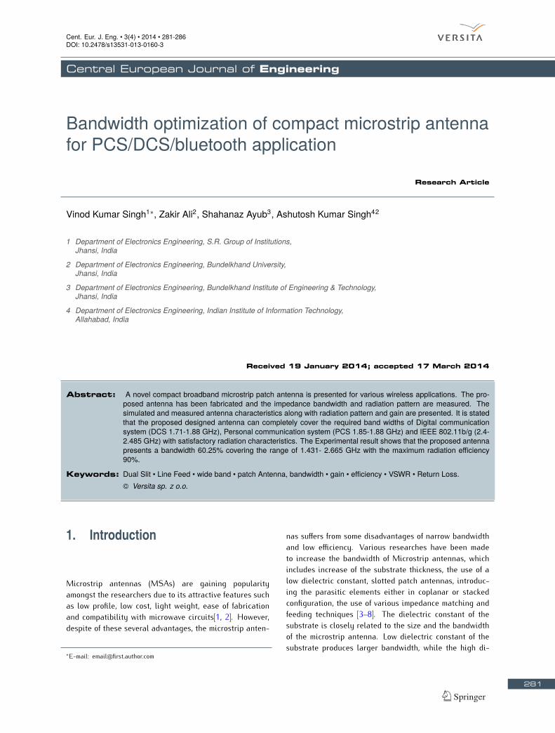
Parameters Value(mm)Lg 40Wg 60W 31L2 13.0W2 4.0L3 9L1 10.8W1 4.0length L1, respectively. The optimized design parametersof the proposed patch antenna are shown in table 1. Theparallel slots are introduced on the patch with glass epoxysubstrate provide bandwidth enhancement. The proposedradiating patch comprises slots symmetrically surround-ing near the excitation probe pin so as to obtain goodimpedance bandwidth. Adding two more slots of same di-mension of width W2 and length L3 on the patch eventu-ally improve the overall impedance bandwidth and betterimpedance matching. The presences of two-slots restrictthe patch currents as well as the two-slots on the patchreduce the size of the proposed patch The photograph ofthe designed antenna is shown in Figure 2.For an efficient radiator, a practical width that leads to
good radiation efficiencies is given by equation (1).For lowfrequencies the effective dielectric constant is essentiallyconstant. At intermediate frequencies its values begin tomonotonically increase and eventually approach the val-ues of the dielectric constant of the substrate. The initialvalues (at low frequencies) of the effective dielectric con-stant are referred to as the static values, and they aregiven by equation (2). Because the dimensions of thepatch are finite along the length and width, the fields atthe edges of the patch undergo fringing. Due to the fring-ing effects, electrically the patch of the microstrip antennalooks greater than its physical dimensions. For the prin-cipal E -plane ( xy -plane),the dimensions of the patchalong its length have been extended on each end by adistance ∆l ,which is a function of the effective dielec-tric constant εreff and the width to height ratio ( W/h).A very popular and practical approximate relation for thenormalized extension of the length is [9–11]w = c2f√(εr + 1)/2 (1)
Since the length of the patch has been extended by ∆l oneach side; the effective length of the patch is nowL = 12fr√εreff√µoεo (4)
Where,c = Velocity of Lightεr = is dielectric constant of the substratef = antenna working frequencyW = width of the patchL = Length of the patchh = height of substrate∆l = normalized extension of the length of the patch
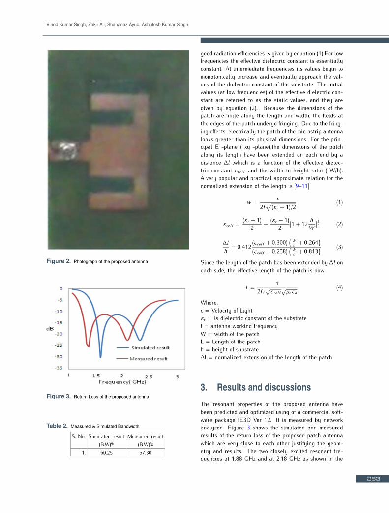
3. Results and discussionsThe resonant properties of the proposed antenna havebeen predicted and optimized using of a commercial soft-ware package IE3D Ver 12. It is measured by networkanalyzer. Figure 3 shows the simulated and measuredresults of the return loss of the proposed patch antennawhich are very close to each other justifying the geom-etry and results. The two closely excited resonant fre-quencies at 1.88 GHz and at 2.18 GHz as shown in the
283
Bandwidth optimization of compact microstrip antenna for PCS/DCS/bluetooth application
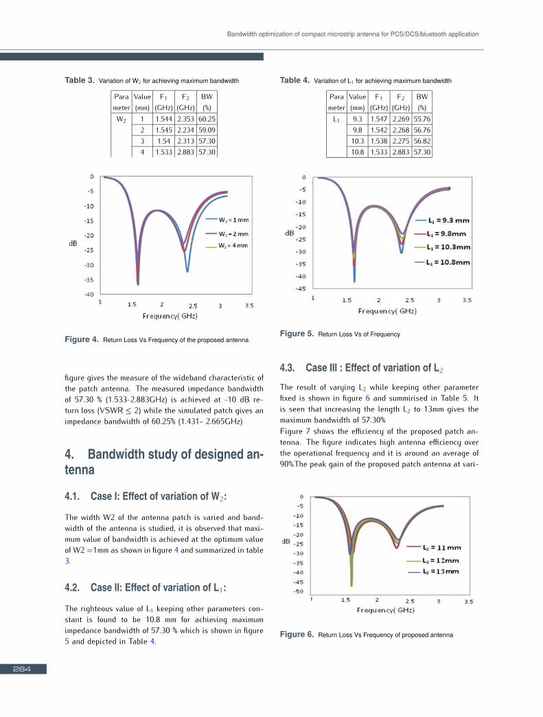
Table 3. Variation of W2 for achieving maximum bandwidth
Para Value F1 F2 BWmeter (mm) (GHz) (GHz) (%)W2 1 1.544 2.353 60.252 1.545 2.234 59.093 1.54 2.313 57.304 1.533 2.883 57.30
Figure 4. Return Loss Vs Frequency of the proposed antenna
figure gives the measure of the wideband characteristic ofthe patch antenna. The measured impedance bandwidthof 57.30 % (1.533-2.883GHz) is achieved at -10 dB re-turn loss (VSWR ≤ 2) while the simulated patch gives animpedance bandwidth of 60.25% (1.431- 2.665GHz)4. Bandwidth study of designed an-tenna
4.1. Case I: Effect of variation of W2:
The width W2 of the antenna patch is varied and band-width of the antenna is studied, it is observed that maxi-mum value of bandwidth is achieved at the optimum valueof W2 =1mm as shown in figure 4 and summarized in table3.4.2. Case II: Effect of variation of L1:
The righteous value of L1 keeping other parameters con-stant is found to be 10.8 mm for achieving maximumimpedance bandwidth of 57.30 % which is shown in figure5 and depicted in Table 4.
Table 4. Variation of L1 for achieving maximum bandwidth
Para Value F1 F2 BWmeter (mm) (GHz) (GHz) (%)L1 9.3 1.547 2.269 55.769.8 1.542 2.268 56.7610.3 1.538 2.275 56.8210.8 1.533 2.883 57.30
Figure 5. Return Loss Vs of Frequency
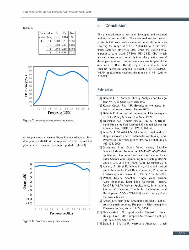
4.3. Case III : Effect of variation of L2The result of varying L2 while keeping other parameterfixed is shown in figure 6 and summirised in Table 5. Itis seen that increasing the length L2 to 13mm gives themaximum bandwidth of 57.30%Figure 7 shows the efficiency of the proposed patch an-tenna. The figure indicates high antenna efficiency overthe operational frequency and it is around an average of90%.The peak gain of the proposed patch antenna at vari-
Figure 6. Return Loss Vs Frequency of proposed antenna
Table 5. Para Value F1 F2 BWmeter (mm) (GHz) (GHz) (%)L2 10 1.608 2.234 51.5011 1.583 2.254 53.8612 1.558 2.254 53.5613 1.533 2.883 57.30
Figure 7. Efficiency Vs frequency of the antenna
ous frequencies is shown in Figure 8, the maximum achiev-able gain is 6.20 dBi at the frequency of 2.3 GHz and thegain is better compare to design reported in [17–21]
Figure 8. Gain Vs frequency of the antenna
5. ConclusionThe proposed antenna has been developed and designedand tested successfully. The simulated results demon-strate that it has a wide impedance bandwidth of 60.25%covering the range of 1.431- 2.665GHz with the max-imum radiation efficiency 90%, while the experimentalimpedance band width 57.30%(1.533-2.883 GHz) whichare very close to each other defining the practical use ofdeveloped antenna. The maximum achievable gain of theantenna is 6.20 dBi.The developed line feed wide bandcompact microstrip antenna is suitable for DCS/PCS/WLAN applications covering the range of (1.431 GHz to2.665GHz).References
[1] Balanis C. A., Antenna Theory, Analysis and DesignJohn Wiley & Sons New York 1997[2] Kumar Girish, Ray K.P., Broadband Microstrip an-tennas, Norwood: Artech House 2003.[3] Balanis C. A., Advanced Engineering Electromagnet-ics, John Wiley & Sons, New York, 1989.[4] Deshmukh A.A., Kadam Ameya, Ray K. P., Broad-band Proximity Fed Modified E-shaped MicrostripAntenna, Proc. IEEE, Vol. 978-1, 2011.4.[5] Islam M. T., Shakib M. N., Misran N., Broadband E-Hshaped microstrip patch antenna for wireless systems,Progress In Electromagnetics Research, PIER 98, pp.163-173, 2009.[6] Srivastava Stuti, Singh Vinod Kumar, Bow-TieShaped Printed Antenna for UMTS/WLAN/WiMAXapplications, Journal of Environmental Science, Com-puter Science and Engineering & Technology (ISSN:2278 179X), Vol.3.No.1, 0261-0268, December 2013.[7] Ansari J. A., Singh P., Dubey S. K., H-Shaped stackedpatch Antenna for Dual Band Operation, Progress InElectromagnetics Research B, Vol. 5, 291-302, 2008.[8] Pathak Rajeev Shankar, Singh Vinod Kumar,Ayub Shahanaz, Dual band Microstrip Antennafor GPS/ WLAN/WiMax Applications, InternationalJournal of Emerging Trends in Engineering andDevelopment(ISSN:2249-6149),Issue2 Vol.7,pp154-159,November 2012.[9] Ansari, J. A., Ram R. B., Broadband stacked U-slot mi-crostrip patch antenna, Progress In ElectromagneticResearch Letters, Vol. 4, 17-24, 2008.[10] Hammerstad E.O., Equations for Microstrip CircuitDesign, Proc. Fifth European Micro-wave Conf., pp.268-272, September 1975.[11] Bahl I. J., Bhartia P., Microstrip Antennas, Artech285
Bandwidth optimization of compact microstrip antenna for PCS/DCS/bluetooth application
House, Dedham, MA, 1980.[12] Kulkarni Nagraj, Mulgi S. N., Satnoor S. K., Designand Development of Triple Band Tunable MicrostripAntenna, Microwave and Optical Technology LettersVol. 54, No. 3, pp 614-617March 2012.[13] Veysi Mehdi, Kamyab Manouchehr, Jafargholi Amir,Single-Feed Dual-Band Dual-Linearly PolarizedProximity-Coupled Patch Antenna, IEEE Antennasand Propagation Magazine, Vol. 53, No.1, February2011.[14] Alkanhal M. A. S., Composite Compact Triple-BandMicrostrip Antennas, Progress In ElectromagneticsResearch, PIER 93, 221-236, 2009.[15] Singh Vinod K., Ali Zakir, Singh Ashutosh Kumar,Dual wideband stacked patch antenna for WiMax andWLAN application, Proc. IEEE-CICN- 2011, PrintISBN: 978-1-4577-2033-8 pp- 315 - 318. Gwalior,India.[16] Singh Vinod K., Ali Zakir, Design of Compact TripleBand Microstrip Antenna for Wireless Communica-tion, International Journal of Electronics and Com-munication Engineering. ISSN 0974-2166 Volume 3,Number 1 (2010), pp. 323-330.[17] Ghalibafany J., Attari A. R., A new Dual-Band Mi-crostrip Antenna with U-Shaped slot, Progress In
Electromagnetics Research C, Vol. 12, 215-223, 2010.[18] Mishra A., Singh P., Yadav N. P., Ansari J. A., Com-pact Shorted Microstrip patch Antenna for Dual BandOperation, Progress In Electromagnetics Research C,Vol. 9, 171-182, 2009.[19] Singh Vinod Kumar, Ali Zakir, Singh A. K., AyubShahanaz ,Dual band triangular slotted stacked mi-crostrip antenna for wireless applications, CentralEuropean Journal of Engineering (CEJE), SpringerISSN: 1896 1541Volume 3, Issue 2, pp 221-225 June,2013.[20] Singh Vinod Kumar , Ali Zakir, Ayub Shahanaz,Ashutosh Kumar Singh, A wide band Compact Mi-crostrip Antenna for GPS/DCS/PCS/WLAN Applica-tions, a book chapter in the book entitled "Intelli-gent Computing, Networking, and Informatics", (BookISBN: 978-81-322-1664-3) Chapter 113, pp: 183-204,Springer.[21] Singh A. K., Kabeer R.A., Singh Vinod. K., Ali Z., Per-formance Analysis of First Iteration Koch Curve Frac-tal Log Periodic Antenna of Varying Angles, CentralEuropean Journal of Engineering (CEJE), SpringerISSN: 1896-1541Volume 3, Issue 1, pp 51-57 March2013.