Progress In Electromagnetics Research, Vol. 157, 49–61, 2016 Bandwidth Tuning in Transistor Embedded Metamaterials Using Variable Resistance John P. Barrett 1 , Alexander R. Katko 1, 2 , and Steven A. Cummer 1, * Abstract—Metamaterials have been previously loaded with diodes and other types of passive circuit elements. Transistors offer an alternative to these established loading elements to expand the possible capabilities of metamaterials. With embedded transistors, additional degrees of freedom are achieved and lay out the architecture for more complex electromagnetic metamaterial design. A mathematical analysis of transistor loaded SRR unit cells is described in which the transistor acts as a variable resistor. From the mathematical analysis, we calculate transmission coefficients for a single unit cell. We then experimentally measure two SRRs with tunable quality factors and thus tunable bandwidth based upon modulating the effective loading circuit resistance to confirm the calculations. From the agreement between the calculated and measured transmission coefficients, we expand the analysis to show that a slab of more densely packed unit cells can achieve negative permeability with varying degrees of dispersion. 1. INTRODUCTION Metamaterials have introduced a new method of creating effective artificial materials with various novel properties. Examples of these properties are negative permeability [1, 2], negative permittivity [3], and negative index of refraction [4, 5]. Correctly engineering and controlling these properties has yielded advances in cloaking [6], lensing [7, 8], and antenna design [9–11]. However, for all of these properties to be expressed in the manner required for the aforementioned applications, metamaterials need to be composed of resonant inclusions. Resonant structures are inherently bandwidth and loss limited. To overcome the narrow bandwidth limitation, tunable RF metamaterials have been created by embedding diodes [12, 13], MEMS switches [14], and ferromagnetic elements [15, 16]. These are all passive components and are used to tune the value of the resonant frequency, with varying degrees of continuity. Tuning the resonant frequency value is only one type of tunability for a resonant structure. The resonance quality factor, which is determined from the bandwidth and loss of the resonator, can also be tuned to affect the frequency response of a metamaterial [17]. Transistors are three or four terminal devices (as opposed to the passive two-terminal devices such as diodes and capacitors) that have found applications in many aspects of circuits and systems as well as providing an alternative to the previously mentioned embedded devices. At the circuit level, transistors are used for amplication, oscillation generation, and switching, providing several crucial active functions in electronic circuits. However, transistors have only recently been embedded in metamaterials through simple circuits and applications [18–21]. The extra terminals provide more control over the characteristics of the unit cell, providing the additional possibility for tuning the bandwidth. This work will highlight the physics of using a metal-oxide-semiconductor field effect transistor (MOSFET) for tuning both the resonant frequency Received 20 July 2016, Accepted 9 September 2016, Scheduled 19 October 2016 * Corresponding author: Steven A. Cummer ([email protected]). 1 Department of Electrical and Computer Engineering, Duke University, Durham, NC 27708, USA. 2 Now with Pivotal Communications, Bellevue, WA 98005, USA.
Transcript
Progress In Electromagnetics Research, Vol. 157, 49–61, 2016
Bandwidth Tuning in Transistor Embedded Metamaterials UsingVariable Resistance
John P. Barrett1, Alexander R. Katko1, 2, and Steven A. Cummer1, *
Abstract—Metamaterials have been previously loaded with diodes and other types of passive circuitelements. Transistors offer an alternative to these established loading elements to expand the possiblecapabilities of metamaterials. With embedded transistors, additional degrees of freedom are achievedand lay out the architecture for more complex electromagnetic metamaterial design. A mathematicalanalysis of transistor loaded SRR unit cells is described in which the transistor acts as a variable resistor.From the mathematical analysis, we calculate transmission coefficients for a single unit cell. We thenexperimentally measure two SRRs with tunable quality factors and thus tunable bandwidth based uponmodulating the effective loading circuit resistance to confirm the calculations. From the agreementbetween the calculated and measured transmission coefficients, we expand the analysis to show thata slab of more densely packed unit cells can achieve negative permeability with varying degrees ofdispersion.
1. INTRODUCTION
Metamaterials have introduced a new method of creating effective artificial materials with various novelproperties. Examples of these properties are negative permeability [1, 2], negative permittivity [3], andnegative index of refraction [4, 5]. Correctly engineering and controlling these properties has yieldedadvances in cloaking [6], lensing [7, 8], and antenna design [9–11]. However, for all of these propertiesto be expressed in the manner required for the aforementioned applications, metamaterials need to becomposed of resonant inclusions.
Resonant structures are inherently bandwidth and loss limited. To overcome the narrowbandwidth limitation, tunable RF metamaterials have been created by embedding diodes [12, 13], MEMSswitches [14], and ferromagnetic elements [15, 16]. These are all passive components and are used to tunethe value of the resonant frequency, with varying degrees of continuity. Tuning the resonant frequencyvalue is only one type of tunability for a resonant structure. The resonance quality factor, which isdetermined from the bandwidth and loss of the resonator, can also be tuned to affect the frequencyresponse of a metamaterial [17].
Transistors are three or four terminal devices (as opposed to the passive two-terminal devices suchas diodes and capacitors) that have found applications in many aspects of circuits and systems as well asproviding an alternative to the previously mentioned embedded devices. At the circuit level, transistorsare used for amplication, oscillation generation, and switching, providing several crucial active functionsin electronic circuits. However, transistors have only recently been embedded in metamaterials throughsimple circuits and applications [18–21].
The extra terminals provide more control over the characteristics of the unit cell, providing theadditional possibility for tuning the bandwidth. This work will highlight the physics of using ametal-oxide-semiconductor field effect transistor (MOSFET) for tuning both the resonant frequency
Received 20 July 2016, Accepted 9 September 2016, Scheduled 19 October 2016* Corresponding author: Steven A. Cummer ([email protected]).1 Department of Electrical and Computer Engineering, Duke University, Durham, NC 27708, USA. 2 Now with PivotalCommunications, Bellevue, WA 98005, USA.
50 Barrett, Katko, and Cummer
and resonance bandwidth, helping set the foundation for future applications of transistor embeddedmetamaterials. Design of metamaterials with a tunable quality factor allows for the creation of ametamaterial that can be configured through bandwidth modulation as well as resonant frequencymodulation.
This work demonstrates how to create a metamaterial with a tunable bandwidth that utilizesa transistor as a variable linear resistor. Section 2 will review the important physics of passiveelements and transistors that will allow for the constructing such a metamaterial. Section 3 willapply the developed physical models to describe a metamaterial with a variable bandwidth followed byexperimental characterization. The final section will explain how to modify the transistor’s configurationwithin the SRR in order to achieve minimal resonant frequency change while tuning the bandwidth byutilizing a different tunable element within the structure of the transistor.
2. METHOD OF QUALITY FACTOR TUNING
To design and quantify a resonant circuit, a mathematical quantity must be derived that accuratelydescribes the bandwidth (shape) of the resonance. An important figure of merit for any passive orresonant element is its quality factor (Q). Q is numerically defined as the ratio of stored energy todissipated energy (Eq. (1)) [22, 23].
Q = ωWstored
Pdissipated(1)
For large values of Q, the element acts more like an ideal energy storage element and for small values ofQ, the element is effectively an attenuator (or resistor). High Q elements and resonators are not alwaysthe best types of inclusions for every application, but being able to quantify the ideality of passivecomponents is important for the characterization of a system.
A simple passive SRR can be reduced to a series RLC circuit for the purposes of metamaterialdesign [1]. Based upon the effective circuit parameters of such a SRR, the values of Q for the circuitequivalent series inductor and capacitor are calculated using Eqs. (2) and (3).
Qc =1
ωCR(2)
Ql =ωL
R(3)
The Q of the series RLC circuit at the resonant frequency is then determined by substituting ω0 inplace of ω and solving for either Ql or Qc.
Q =ω0L
R=
1R
√L
C(4)
From Eq. (4), the simplest method to vary Q while maintaining constant ω0 is to tune the loop seriesresistance R (both L and C can also be used to tune Q but the LC product must remain constant).The structure of a transistor includes several different tunable elements, including a tunable resistorlocated between the drain and source terminals. This is the element that will be exploited to create ametamaterial with a tunable quality factor.
MOSFETs have 3 regions of operation: cutoff (or subthreshold), linear, and saturation. All regionsof operation provide a tunable resistance, but the mechanism and range of resistance values is slightlydifferent in each region. To define the operating regions, the threshold voltage (VT ) must be defined. Inthis work, VT is defined as the bias required to attract enough electrons to create the inverted channel(the concentration of electrons in the channel is equal to the concentration of holes in the bulk awayfrom the gate oxide). In cutoff, the gate to source voltage (VGS) is less than the threshold voltage(VGS < VT ). Under this bias condition, the conducting channel is not fully present but there is a smallcurrent can still flow from drain to source if another voltage is applied across those two terminals.
The IDS current equation in the cutoff region is as follows in Eq. (5) [24] (the primary parameters tofocus on are VGS , VT , and VDS as the rest are constants determined from the physical semiconductor).
IDS = k′WL
(m − 1)(
kBT
q
)2
eq(VGS−VT )/mkBT (1 − e−qVDS/kBT ) (5)
Progress In Electromagnetics Research, Vol. 157, 2016 51
IDS is not solely dependent on a single voltage, unlike current flowing a diode, but rather two voltages.VDS dictates the current in a reverse bias diode-like equation while the application of VGS pulls extraconducting electrons to the surface in the bulk, partially forming a conducting channel.
The second bias region for a MOSFET is the linear region. When VGS is raised to voltages greaterthan VT , the conducting channel is fully formed and allows for significant current flow from drainto source in the device. The current generated from the reverse biased junction becomes negligiblecompared with the current that flows through the channel and changes the current-voltage characteristic(Eq. (6) [25–27]).
IDS = k′WL
[(VGS − VT )VDS − V 2
DS
2
](6)
IDS in this region becomes linearly related to VGS and quadratically related to VDS , a stark contrastcompared with the exponential relationships from the current equation for the cutoff region (Eq. (5)). IfVDS is kept small, there is an increase in linearity between the current and voltage. The control of IDS
with VGS in the cutoff and linear regions with respect to creating a tunable resistance will be looked atin Section 3.
If VDS is increased to VGS −VT , the conducting channel becomes “pinched-off.” When the channelis pinched-off, the MOSFET reaches the saturation operating region. The current-voltage characteristicchanges from Eq. (6) to Eq. (7) [25–27] (again, VGS, VT , and VDS are the primary parameters to focuson to understand the transistor behavior).
IDS =k′
2W
L(VGS − VT )2(1 + λVDS) (7)
Once a MOSFET is in saturation, the current flow becomes nearly constant with increasing VDS sincepinching off the conducting channel restricts the concentration of carriers. IDS does increase with VDS
due to the channel length modulation effect, but the rate of change is much smaller than in the linearregion.
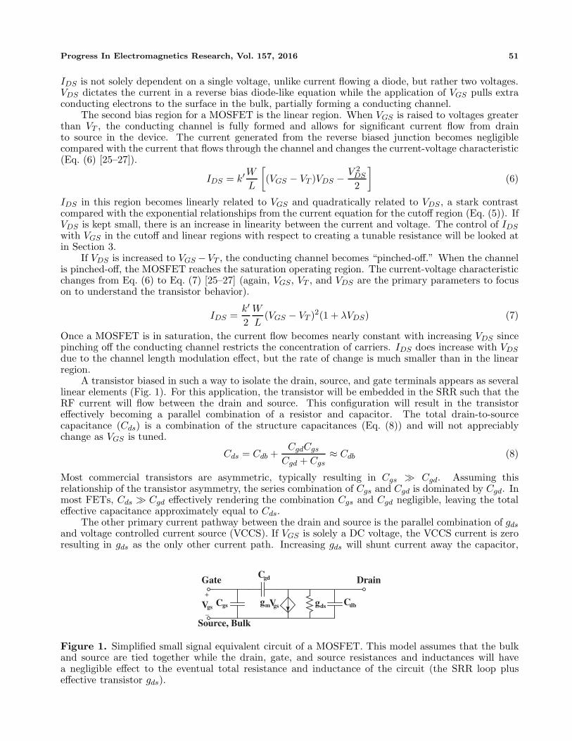
A transistor biased in such a way to isolate the drain, source, and gate terminals appears as severallinear elements (Fig. 1). For this application, the transistor will be embedded in the SRR such that theRF current will flow between the drain and source. This configuration will result in the transistoreffectively becoming a parallel combination of a resistor and capacitor. The total drain-to-sourcecapacitance (Cds) is a combination of the structure capacitances (Eq. (8)) and will not appreciablychange as VGS is tuned.
Cds = Cdb +CgdCgs
Cgd + Cgs≈ Cdb (8)
Most commercial transistors are asymmetric, typically resulting in Cgs � Cgd. Assuming thisrelationship of the transistor asymmetry, the series combination of Cgs and Cgd is dominated by Cgd. Inmost FETs, Cds � Cgd effectively rendering the combination Cgs and Cgd negligible, leaving the totaleffective capacitance approximately equal to Cds.
The other primary current pathway between the drain and source is the parallel combination of gds
and voltage controlled current source (VCCS). If VGS is solely a DC voltage, the VCCS current is zeroresulting in gds as the only other current path. Increasing gds will shunt current away the capacitor,
Gate Drain
Source, Bulk
Cgs gmVgsCdbgds
Cgd
+
_Vgs
Figure 1. Simplified small signal equivalent circuit of a MOSFET. This model assumes that the bulkand source are tied together while the drain, gate, and source resistances and inductances will havea negligible effect to the eventual total resistance and inductance of the circuit (the SRR loop pluseffective transistor gds).
52 Barrett, Katko, and Cummer
changing the quality factor of Cds. Taking the partial derivative of Eq. (5) with respect to VDS , theeffective gds for the transistor under subthreshold conditions is obtained.
gds =∂IDS
∂VDS= k′W
L(m − 1)
(kBT
q
)e
q(VGS−VT −mVDS)
mkBT (9)
An important feature within Eq. (9) is that the change in conductance becomes very rapid. WhenVGS is increased to near VT , the conducting channel between is nearly formed and the Q of the effectivecapacitor is very small compared to a physical lumped capacitor. At the bias point VGS ≥ VT , theconducting channel between the drain and source is fully present and the embedded transistor’s effectiveoperating region switches from subthreshold to linear.
In the linear region, the transconductance term gm still remains near zero meaning the gds elementwill still be the primary resistive current carrying element. In the linear region, if VDS is small, thequadratic term in Eq. (6) becomes negligible (Eq. (10)).
IDS = k′WL
(VGS − VT )VDS (10)
gds =∂IDS
∂VDS= k′W
L(VGS − VT ) (11)
Eq. (10) demonstrates a current characteristic similar to that of a resistor since IDS and VDS are linearlyproportional. By increasing VGS , nearly all the RF current will be shunted away from the capacitor,reducing the effect that Cds will have on the circuit. However, at a certain voltage, the insulating oxidewill begin to break down due to the large electric field across the gate oxide, destroying the variableresistor effect. As the oxide will no longer be isolating the gate and bulk, there will not be a potentialdifference between the gate and bulk, thus eliminating the electric field generated from the gate to thebulk and physically destroying the transistor.
VDS can be made non-zero to bias the transistor in the saturation region but will make gds verysmall.
gds =∂IDS
∂VDS=
12λk′W
L(VGS − VT )2 (12)
Even with the square dependence on VGS − VT , the current does not appreciably change with VDS .With the slope of the current nearly flat, the effective conductance reduces to something similiar inmagnitude to the cutoff/subthreshold conductance where most of the small signal current flows throughthe capacitor. The VCCS then becomes the tunable element of interest, but is only tunable if thegate-to-source voltage is a small signal RF voltage and not only a DC voltage. Using the VCCS as atunable element embedded in a metamaterial is discussed in Section 4.
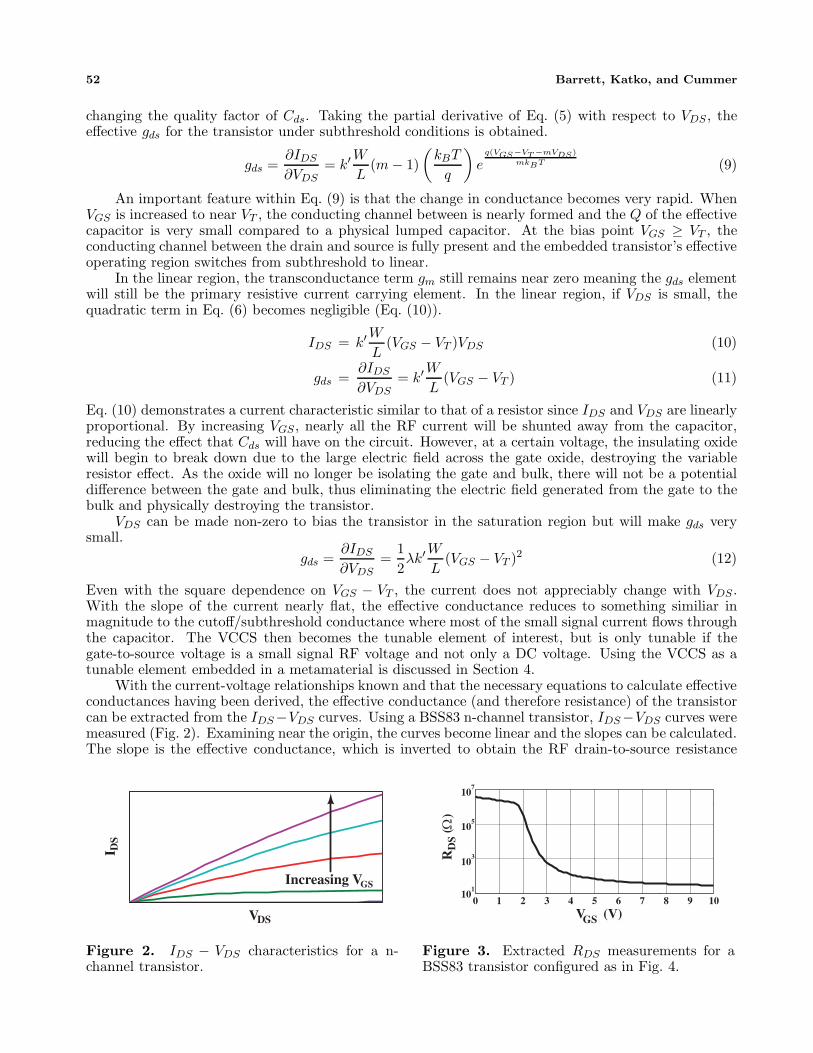
With the current-voltage relationships known and that the necessary equations to calculate effectiveconductances having been derived, the effective conductance (and therefore resistance) of the transistorcan be extracted from the IDS−VDS curves. Using a BSS83 n-channel transistor, IDS−VDS curves weremeasured (Fig. 2). Examining near the origin, the curves become linear and the slopes can be calculated.The slope is the effective conductance, which is inverted to obtain the RF drain-to-source resistance
VDS
I DS
Increasing VGS
Figure 2. IDS − VDS characteristics for a n-channel transistor.
0 1 2 3 4 5 6 7 8 9 1010
1
103
105
107
VGS (V)
RD
S ( Ω
)
Figure 3. Extracted RDS measurements for aBSS83 transistor configured as in Fig. 4.
Progress In Electromagnetics Research, Vol. 157, 2016 53
(Fig. 3). The gate was directly connected to a DC control voltage while the source is connected toDC ground, creating the necessary VGS to control the conductance of the channel between the drainand source. The drain is connected to the source by a resistor, which limits the minimum effectiveconductance (therefore determining the minimum loss of the capacitive structure) and sets the VDS tozero. As expected, the resistance decreases exponentially in the cutoff region (consistent with Eq. (9))and decreases much more gradually in the linear region (consistent with Eq. (11)).
3. ANALYSIS, SIMULATION, AND MEASUREMENT OF A SRR WITH TUNABLEQ
Starting with the equivalent circuit model of the transistor-embedded SRR, the analysis from Section 2can be employed to determine the exact mathematical relationship between the circuit parameters andthe quality factor. Eq. (4) can also be determined from the fact that the energy stored in the capacitorand inductor are equal at the resonant frequency [22]. Revisiting the initial definition of Q (Eq. (1)),the Q of the SRR equivalent circuit is determined through the summation of the stored energy in thecapacitors and inductors (Eq. (13)) and the power dissipation caused by the resistors (Eq. (14)).
Wst = WM + WE =14|ILM
|2LM +14CM |VCM
|2 +14Ct|VCt |2 (13)
Pdis =12|IRM
|2RM +12|IRt |2Rt (14)
The voltage across transistor capacitance (VCt) is related to the current (IRt) flowing through theresistive path of the transistor (Eq. (15)) while the current through the resistor is related to theimpedance of the capacitance and resistance (Eq. (16)).
VCt = IRtRt (15)
IRt =ILM
jωCtRt + 1(16)
Using the fact that the stored electric and magnetic energy are equal at resonance [22] and IRM= ILM
,Eq. (16) can be substituted into Eq. (14) to determine the Q of the transistor-embedded SRR equivalentcircuit at resonance (Eq. (17)).
Q = ω02WM
Pdissipated= ω0
12|ILM
|2L12|ILM
|2RM +12|ILM
|2Rt1
|jω0CtRt|2(17)
Eq. (17) simplifies further to Eq. (18).
Q =ω0LM
RM +Rds
(ω0CdsRds)2 + 1
(18)
At the extreme positive values of the transistor resistance, the equation to derive Q simplifies to a formconsistent with that of a normal passive SRR (Eq. (4)). Eq. (18) also allows for the analysis of thetransistor-embedded SRR in bias regions such that the transistor resistance isn’t either very large orvery small.
The analysis of the equivalent circuit model is still not finished. Due to the dynamics of theincremental Rt, there will be a change in the resonant frequency. The above analysis used to derive anexpression for Q did not explicitly require that ω0 be already known. For the resonant system to befully characterized, an expression relating ω0 and the equivalent circuit parameters must be derived.
Using the basic definition of a resonance, the total reactance of the transistor-embedded equivalentcircuit will sum to zero at ω0. The total equivalent circuit impedance is calculated in Eq. (19).
Z = RM + jωLM − j
ωCM+
Rt
1 + jωCtRt(19)
54 Barrett, Katko, and Cummer
The impedance calculation also simplifies to the basic series RLC impedance equation at the extremevalues of Rt, yielding the maximum and minimum limits of the resonant frequency. The reactancecalculation can be further simplified to Eq. (20).
X = Im{Z} =ω4LMCMC2
dsR2ds + ω2(LMCM − (CdsRds)2 − CMCdsR
2ds) − 1
ωC(1 + ω2C2dsR
2ds)
(20)
The reactance has poles at the zero frequency and two conjugate imaginary frequencies so the calculationof the reactance zeros can be done without running into higher order poles and zeros. Setting thenumerator equal to zero and using a dummy variable to reduce the order of polynomial (set x = ω2),the resonant frequency is calculated from the effective circuit parameters using the quadratic formula(Eq. (21)).
x =(CdsRds)2 + CM (CdsR
2ds − LM )
2LMCMC2dsR
2ds
±√
[CM (LM − CdsR2ds) − (CdsRds)2]2 + 4LMCMC2
dsR2ds
2LMCMC2dsR
2ds
(21)
Taking the square root of x yields four possible solutions for the resonant frequency. Because all theeffective circuit parameters are real valued and positive, only a single solution for ω is real and positiveyielding a single valued resonant frequency.
Based upon Eqs. (18) and (19), a transistor-embedded SRR as configured in Fig. 4 can be fullyanalyzed mathematically. It is important to emphasize that the gate voltage is a DC quantity and thatgate is effective isolated from the drain, source, and bulk to confirm that the system is passive andwill not have issues typically associated active transistor circuits. Using the extracted effective circuitparameters of the transistor and SRR loop, the analytical dependence of the resonant frequency andresonance quality on the gate voltage can be plotted (Fig. 5).
When Rds is very high (significantly greater than the transistor capacitance impedance), theresonance Q is higher than in other bias regions. Under the high resistance condition, most of theinduced RF current flows through the transistor like an effective low-loss capacitor which adds near-zero resistive loss to loop. When the drain-to-source resistance is very low (significantly lower than the
ControlVoltage
ControlVoltage
(a) (b)
Lm Cm Rm
Rt
Ct=Cdb
=1/gds
Figure 4. Diagram (a) and effective circuitequivalent (b) of a transistor embedded SRR. Thetransistor is embedded such that the gate is solelyDC biased and RF current effectively only owsfrom drain to source. The FET bulk is tied to thesource to avoid changes to the threshold voltagewith a large-valued resistor connected across thesource and drain to avoid hysteretic effects fromthe back-to-back junctions (DC bias network notshown).
0 2 4 6 8 10740
770
800
830
VGS (V)
Fre
quen
cy (
MH
z)
Q
0
10
20
30
Q f
0
Figure 5. Calculated Q and f0 for transistor-embedded SRR using estimated effective circuitparameters for the loop and transistor.
Progress In Electromagnetics Research, Vol. 157, 2016 55
transistor capacitance impedance), the resonance quality starts to increase with an increase in VGS .At this bias condition, the transistor resistance decreases, increasing Q (as expected from Eq. (4)). Inthe bias region when the drain-to-source resistance is roughly equivalent to the transistor capacitanceimpedance, the RF current is split approximately equally through the resistive and capacitive paths.Due to the large impedance across both paths (CDS of the BSS83N is close to 1.5 pF, which yields animpedance magnitude of around 150 Ω at 750 MHz), the generated current is limited, decreasing theresonance quality and reducing the polarizability of the SRR.
Once the quality factor and resonant frequency of the effective circuit have been calculated, theeffective permeability can then be determined [28] using Eq. (22) (F is defined as a geometry/fill factorrelated to the unit cell density).
μr ≈ 1 + χm ≈ 1 +Fω2
ω20 − ω2 +
jωω0
Qcircuit
(22)
F =μ0A
2loop
VcellLloop(23)
From the effective μr calculation, the effective index of refraction (n =√
μrεr), normalized impedance(z =
√μr/εr), and transmission (S21) and reflection (S11) parameters can then be calculated (Fig. 7
and Eqs. (24) and (25)) [29] (since the SRR is a magnetic particle, εr is assumed to be 1).
S−121 =
[cos(nkd) − j
2
(z +
1z
)sin(nkd)
]ejkd (24)
S11 = −12j
(z − 1
z
)sin(nkd)S21e
jkd (25)
To experimentally confirm the calculated values derived from the effective circuit quality factor andother geometric factors, the transistor-embedded metamaterial unit cell was created and fabricated(Fig. 6) using the aforementioned BSS83 transistor (one of the few commercial transistors that have aphysical bulk contact rather than an internal connection between the bulk and the source). The SRRwas placed in a TEM waveguide and S21 was measured (Fig. 7(c)).
Port 1
SRR placementin waveguide
EmbeddedTransistor
Open (Magnetic)Boundaries Port 2
Figure 6. Fabricated FET-embedded unit cell (also seen in [21]). The SRR conducting loop connectsthe drain and source of the transistor with bias wires heading to the source (ground) and gate (VGS).The waveguide is comprised by two conducting plates 6 cm apart with open boundaries which allow forthe bias wires to travel to the unit cell with the bias circuitry being located within the unit cell. Theunit cell was fixed in the waveguide such that the loop was parallel to the magnetic field component ofthe incident wave.
Comparing the experimentally measured data with the simulation data, the measured S21 curvesdemonstrate the expected behavior, agreeing reasonably well in both resonant frequency and magnitude.There is a shift in the SRR resonant frequency corresponding to the low resistance and high resistancevalues from Fig. 3, as well as a bias range in which the resonance quality is reduced to a minimum(corresponding to the resistance range around 1 kΩ).
With the experimental measurements confirming the validity of the mathematical analysis, theresults can be extended to predict the effective material parameters if a slab of such unit cells iscreated. In the previous analytic calculations, the F factor in Eq. (22) was derived using effective
56 Barrett, Katko, and Cummer
(a)
(b) (c)
Figure 7. (a) Calculated S11, (b) calculated S21, and (c) measured S21 of a single transistor-embeddedunit cell as described in Fig. 4 using the setup described in Fig. 6.
600 650 700 750 800 850 900Frequency (MHz)
-2
-1
0
1
2
3
4
Re{μ
r}
2.5 V2.7 V3 V4 V10 V
600 650 700 750 800 850 900Frequency (MHz)
-4
-3
-2
-1
0
1
Im{μ
r}
2.5 V2.7 V3 V4 V10 V
(a) (b)
Figure 8. Calculated (a) Re{μr} and (b) Im{μr} of a metamaterial slab comprised by transistor-embedded SRRs such that the unit cell size was 60mm × 60mm × 60 mm. The SRRs configured asshown in Fig. 4 based upon the Q values in Fig. 5.
unit cell dimensions of 60mm × 60mm × 500 mm (based on the approximate dimensions of themeasurement waveguide). If we assume that the slab would be comprised by unit cells with dimensions60mm × 60mm × 60 mm, the F value increases while keeping the other values from Eq. (22) constant.Based on this theoretical increase in unit cell density, meaningful effective material parameters can becalculated (Fig. 8).
From the relative permeability curves, it is clear that such a metamaterial would potentially beable to still realize a region with negative permeability and that the bandwidth of such a region could becontrolled. There are also curves at bias voltages of 2.5 and 2.7 V in Fig. 8(a) that predict that such aslab of metamaterial could create a nearly dispersionless frequency region. Looking at the correspondingdata dipicted in Fig. 8(b) shows that this behavior is also associated with the bias condition requiredfor minimum loss magnitude. This metamaterial state corresponds to the circuit bias in which theeffective circuit Q reaches a minimum. This potentially reveals a way to passively create a relativelydispersionless material with μr near zero.
There is a region around the transistor threshold voltage (around 2 V) in which the resonantfrequency and bandwidth changes rapidly, which is ideal for mixing [21]. Once the bias voltage isgreater than the threshold voltage, the resonant frequency changes less drastically with changes involtage, but the resonance quality steadily increases as the voltage continues to increase. The resonant
Progress In Electromagnetics Research, Vol. 157, 2016 57
frequency still changes appreciably, however, which is undesirable in some applications. To minimizethe frequency shift, a modification to the transistor circuitry must be made.
4. IMPROVED BANDWIDTH TUNING
The previous section looked at the nMOSFET under cutoff and linear biasing with only a mention of thesaturation operating region. This is due to the large differential resistance (gds) between the source anddrain that occurs under this biasing condition if the gate voltage is a purely DC voltage. As mentionedin the previous section, this would diminish the gate voltage’s effect on the quality factor. To exploitthe effective VCCS element in the small signal model, gm and Vgs must both be non-negligible.
If the drain and gate are connected together, a two terminal element is created and the transistoris said to be diode connected. This changes the small signal model in Fig. 1 to the model in Fig. 9.In this configuration, there are 4 RF current pathways, Cgs, Cds, gds, and the gmVgs VCCS. The gds
conductor is still governed by Eq. (12), but, as mentioned earlier, does not act as an effective RF shuntfor the capacitor.
The VCCS is the primary tunable object in the diode-connected configuration. The drain to sourcecurrent through this circuit element is controlled by Vgs, but since Vgs = Vds, the current through theVCCS can be rewritten as Eq. (26).
IDS,V CCS = gmVgs = gmVds (26)
The transconductance product reduces to Ohm’s Law since the current is linearly dependent on thevoltage across the element (the conductance of the effective resistive element becoming gm). Using thisequivalency, the total drain to source conductance and capacitance is written as:
gt =1Rt
= gm + gds ≈ gm (27)
Ct = Cdb + Cgs (28)
Drain
Source, Bulk
GateCgd
Cdbgm gdsCgs vgsvgs
+
_
Figure 9. Equivalent small signal model of adiode connected transistor. Note that vgs = vds
in this configuration, turning the VCCS into aneffective resistor (Eq. (26)).
ControlVoltage
ControlVoltage
(a) (b)
Lm Cm Rm
Rt
Ct=Cdb+Cgs
=1/gm
Figure 10. Schematic and diagram of adiode connected transistor embedded SRR. Thetransistor is embedded such that the gate anddrain are tied together. The FET bulk is tiedto the source to avoid changes to the thresholdvoltage with a large-valued resistor connectedacross the source and drain to avoid hystersiseffects from the back to back junctions (DC biasnetwork not shown).
58 Barrett, Katko, and Cummer
108
106
104
102
100
VDS (V)
I DS
(A)
0 1 2 3 4101
103
105
107
109
RD
S ( W
)
IDS
RDS
Figure 11. Measured IDS and RDS of the diode-connected BSS83 transistor. Due to measurementerror (IDS < 100 nA is pushing the accuracylimits of the digital ammeter), the measured deepsubthreshold RDS is very noisy but also greaterthan 1 MΩ.
0 0.5 1 1.5 2 2.5 3 3.5 4VGS =VDS (V)
740
770
800
830
Fre
quen
cy (
MH
z)
0
10
20
30
Q
f0
Q
Figure 12. Analytically calculated resonantfrequency and Q based upon effective equivalentcircuit parameters.
Compared with the capacitance seen in the first configuration (Eq. (8)), the effective capacitance of theelement embedded in the SRR loop is increased. This reduces the effect that the transistor capacitancewill have on the overall loop capacitance, minimizing the change in resonant frequency caused by thechange in voltage across the element.
A diode-connected transistor is embedded within an SRR loop as shown in Fig. 10. As with theprevious configuration, the source and bulk are tied together (preventing the threshold voltage changingdue to the body effect). A large valued resistor is, again, placed in parallel to the drain and source toensure that there are no hysteresis effects within the transistor structure (again, this limits the maximumelement resistance and therefore the maximum Q of the resonating unit cell).
Unlike the first configuration, a significant amount of DC power is required to bias the transistor insaturation. In order for the saturation condition to be reached, the electric field from the drain to thegate to counteract the vertical field generated by the gate when VGS > VT . Under this condition, theconducting channel between the drain and source is fully formed and a voltage difference between thedrain and source must exist. There will be a significant current flowing from the drain to the source,hence a larger amount of DC power will be required for biasing. However, the bias voltages are still DCquantities and if the induced signal power in the unit cell is assumed to be small, the system becomeseffectively passive, even though the active transconductance element is the primary tunable element.
Again using a BSS83 nMOSFET, a current-voltage curve was measured and the effective drain tosource resistance was extracted (Fig. 11). Due to the maximum power limit of the transistor, the voltagerange of interest is also reduced. Comparing Fig. 11 with Fig. 3, the subthreshold region still exhibitsthe large change in resistance that is expected from the exponential current-voltage relationship, butthe element resistance does not decrease to the levels of the resistance at higher voltages as seen in theconfiguration detailed in Section 3. This means that the second resonant dip (the greater VGS valuesin Fig. 7) may not be observed in the diode connected configuration, but the resistance change is largeenough that a wide range of resonance quality factors should be observed.
Following the same procedure outlined in Section 3, S11 (Fig. 13(a)) and S21 (Fig. 13(b)) forthe modified transistor-embedded SRR were calculated based upon the quality factor of the effectivecircuit (Fig. 12). Similar to the parameters calculated from the configuration detailed in Fig. 4, asthe resistance decreases, the resonance quality should decrease. There is a slight decrease in resonantfrequency when the bias voltage increases above the threshold voltage, but this is still a much smallerchange as compared to the resonant frequency changes seen in Fig. 7.
To confirm the analytic results, another unit cell based upon the loop geometry seen in Fig. 6 wasfabricated with the drain and gate connected with a wire (and to drive the transistor into saturationwhen the bias voltage was above the threshold voltage). S21 measurements were similarly obtainedin an open TEM waveguide (Fig. 13(c)) confirming that once the transistor operating characteristicsare such that the transistor operates in saturation, the resonant frequency practically ceases changing(< 2%) as the voltage increases.
Progress In Electromagnetics Research, Vol. 157, 2016 59
(a)
(b) (c)
Figure 13. (a) Calculated S11, (b) calculated S21, and (c) measured S21 from unit cell embedded witha diode-connected BSS83 transistor.
Figure 14. Calculated (a) Re{μr} and (b) Im{μr} of a metamaterial slab comprised by diode-connected-transistor-embedded SRRs such that the unit cell size was 60mm × 60mm × 60 mm. TheSRRs configured as shown in Fig. 10 based upon the Q values in Fig. 12.
In contrast to the simulation data in Fig. 13(b), the measured resonance demonstrates that thebandwidth and resonant frequency increase in the subthreshold operating region. This is explained bythe structure capacitances changing because of varying bias (this was previously ignored in the analysisin Section 3 as Cds was assumed to remain nearly constant with varying VGS and Cgs wasn’t relevantin determining the resonant frequency in that configuration). When the voltage was increased to nearthe threshold voltage, the resonance depth reached a maximum and the resonant frequency becamenearly constant with voltage, in agreement with the simulations. Comparing the S21 measurementsfrom the two configurations, the resonance quality changes much more smoothly and slowly using thediode connected configuration. This shows that using a diode connected transistor can offer a significantrange of resonance quality tuning without modifying the resistance significantly.
To again show the effects that such a tunable metamaterial would have as an effective material, thecircuit quality factors were again used to extend the analysis, similarly to Section 3. The F value waschanged in the exact same way (modifying one of the unit cell dimensions from 500 mm to 60 mm) andthe relative permeability was calculated (Fig. 14). From this extension, a slight shift in the Lorentzianshape is observed and, again, the bandwidth in which the permeability is negative is shown to be tunable.Once again, as the circuit bias modifies the effective circuit Q to its minimum, the relative permeability
60 Barrett, Katko, and Cummer
curves again predict frequency regions in which the metamaterial exhibits μ near zero behavior whilebeing minimally dispersive with reduced loss compared with the other unit cell configurations withnarrower bandwidth.
5. CONCLUSION
The ability for a transistor to be embedded within a metamaterial unit cell for the purposes of frequencytuning and resonance quality tuning has been theoretically developed, analyzed, and experimentallyconfirmed. This work also demonstrates and exploits the versatility of the transistor structure by usinga few of the individual tunable elements derived from the transistor model. The ability to dynamicallycontrol the bandwidth and frequency of resonant structures is instrumental in the further developmentand use of metamaterials and other types of RF structures. Additionally, by controlling both theunit cell density and transistor biasing, a potential design procedure has been developed in which thedispersion can also be controlled without introducing large, prohibitive loss. Future work in this areawould include increasing the quality factor tuning range, further minimizing the resonant frequencychange, and apply one of these types of unit cells to previously studied small antennas (such as thework previously described in [9–11]).
ACKNOWLEDGMENT
This work was supported by a Multidisciplinary University Research Initiative from the Army ResearchOffice (contract No. W911NF-09-1-0539).
REFERENCES
1. Pendry, J., A. Holden, D. Robbins, and W. Stewart, “Magnetism from conductors and enhancednonlinear phenomena,” IEEE Transactions on Microwave Theory and Techniques, Vol. 47, No. 11,2075–2084, 1999.
2. Marques, R., F. Medina, and R. Rafii-El-Idrissi, “Role of bianisotropy in negative permeability andleft-handed metamaterials,” Physical Review B, Vol. 65, 144440, 2002.
3. Schurig, D., J. Mock, and D. Smith, “Electric-field-coupled resonators for negative permittivitymetamaterials,” Applied Physics Letters, Vol. 88, No. 4, 041109, 2006.
4. Smith, D., J. Pendry, and M. Wiltshire, “Metamaterials and negative refractive index,” Science,Vol. 305, No. 5685, 788–792, 2004.
5. Padilla, W., D. Basov, and D. Smith, “Negative refractive index metamaterials,” Materials Today,Vol. 9, No. 78, 28–35, 2006.
6. Schurig, D., J. J. Mock, B. J. Justice, S. A. Cummer, J. B. Pendry, A. F. Starr, and D. R Smith,“Metamaterial electromagnetic cloak at microwave frequencies,” Science, Vol. 314, No. 5801, 977–980, 2006.
7. Pendry, J., “Negative refraction makes a perfect lens,” Physical Review Letters, Vol. 85, 3966–3969,2000.
8. Freire, M., R. Marques, and L. Jelinek, “Experimental demonstration of a = 1 metamaterial lensfor magnetic resonance imaging,” Applied Physics Letters, Vol. 93, No. 23, 231108, 2008.
9. Greegor, R., C. Parazzoli, J. A. Nielsen, M. H. Tanielian, D. Vier, S. Schultz, C. Holloway, andR. Ziolkowski, “Demonstration of impedance matching using a mu-negative (mng) metamaterial,”IEEE Antennas and Wireless Propagation Letters, Vol. 8, 92–95, 2009.
10. Erentok, A. and R. Ziolkowski, “Metamaterial-inspired efficient electrically small antennas,” IEEETransactions on Antennas and Propagation, Vol. 56, No. 3, 691–707, 2008.
11. Ziolkowski, R., P. Jin, and C.-C. Lin, “Metamaterial-inspired engineering of antennas,” Proceedingsof the IEEE, Vol. 99, No. 10, 1720–1731, 2011.
Progress In Electromagnetics Research, Vol. 157, 2016 61
12. Gil, I., J. Garcia-Garcia, J. Bonache, F. Martin, M. Sorolla, and R. Marques, “Varactor-loadedsplit ring resonators for tunable notch filters at microwave frequencies,” Electronic Letters, Vol. 40,No. 21, 1347–1348, 2004.
13. Reynet, O. and O. Acher, “Voltage controlled metamaterial,” Applied Physics Letters, Vol. 84,No. 7, 1198–1200, 2004.
14. Hand, T. and S. Cummer, “Characterization of tunable metamaterial elements using memsswitches,” IEEE Antennas and Wireless Propagation Letters, Vol. 6, 401–404, 2007.
15. Zou, D., A. Jiang, and R.-X. Wu, “Ferromagnetic metamaterial with tunable negative index ofrefraction,” Journal of Applied Physics, Vol. 107, No. 1, 013507, 2010.
16. Hand, T. and S. Cummer, “Frequency tunable electromagnetic metamaterial using ferroelectricloaded split rings,” Journal of Applied Physics, Vol. 103, No. 6, 066105, 2008.
17. Cummer, S., B.-I. Popa, and T. Hand, “Q-based design equations and loss limits for resonantmetamaterials and experimental validation,” IEEE Transactions on Antennas and Propagation,Vol. 56, No. 1, 127–132, 2008.
18. Kodera, T., D. Sounas, and C. Caloz, “Artificial faraday rotation using a ring metamaterialstructure without static magnetic field,” Applied Physics Letters, Vol. 99, No. 3, 2011.
19. Jelinek, L. and J. Machac, “An fet-based unit cell for an active magnetic metamaterial,” IEEEAntennas and Wireless Propagation Letters, Vol. 10, 927–930, 2011.
20. Xu, W., W. Padilla, and S. Sonkusale, “Loss compensation in metamaterials through embeddingof active transistor based negative differential resistance circuits,” Optics Express, Vol. 20, No. 20,22406–22411, 2012.
21. Katko, A., J. Barrett, and S. Cummer, “Time-varying transistor-based metamaterial for tunability,mixing, and efficient phase conjugation,” Journal of Applied Physics, Vol. 115, No. 14, 144501, 2014.
22. Pozar, D., Microwave Engineering , 3rd Edition, John Wiley and Sons, Hoboken, NJ, 2005.23. Steer, M., Microwave and RF Design: A Systems Approach, SciTech Publishing Company, Edison,
NJ, 2010.24. Tsividis, Y., Operation and Modeling of the MOS Transistor , 2nd Edition, Oxford University Press,
New York, NY, 1999.25. Sze, S. and K. Ng, Physics of Semiconductor Devices, 3rd Edition, John Wiley and Sons, Hoboken,
NJ, 2007.26. Taur, Y. and T. Ning, Fundamentals of Modern VLSI Devices, 2nd Edition, Cambridge University
Press, New York, NY, 2009.27. Lee, K., M. Shur, T. Fjeldly, and T. Ytterdal, Semiconductor Device Modeling for VLSI , Prentice-
Hall, Englewood Cliffs, NJ, 1993.28. Cummer, S., B.-I. Popa, and T. Hand, “Q-based design equations and loss limits for resonant
metamaterials and experimental validation,” IEEE Transactions on Antennas and Propagation,Vol. 56, No. 1, 127–132, 2008.
29. Smith, D., S. Schultz, P. Markos, and C. Soukoulis, “Determination of effective permittivity andpermeability of metamaterials from reflection and transmission coefficients,” Physical Review B,Vol. 65, 195104, 2002.