+ All Categories
Home > Documents > BASEBAND IMPLEMENTATION OF AN OFDM SYSTEM …gulak/theses/Jing_Zhang_2005_MASC_thesis.… ·...

BASEBAND IMPLEMENTATION OF AN OFDM SYSTEM …gulak/theses/Jing_Zhang_2005_MASC_thesis.… ·...

Date post: 08-Apr-2018
Category:
Upload: phamcong
View: 218 times
Download: 2 times
Share this document with a friend
137
BASEBAND IMPLEMENTATION OF AN OFDM SYSTEM FOR 60 GHZ RADIOS By Jing Zhang A thesis submitted in conformity with the requirements for the degree of Master of Applied Science Graduate Department of Electrical and Computer Engineering University of Toronto © Copyright by Jing Zhang 2005
Transcript

BASEBAND IMPLEMENTATION OF AN

OFDM SYSTEM FOR 60 GHZ RADIOS

By

Jing Zhang

A thesis submitted in conformity with the requirements

for the degree of Master of Applied Science

Graduate Department of Electrical and Computer Engineering

University of Toronto

© Copyright by Jing Zhang 2005

BASEBAND IMPLEMENTATION OF AN OFDM SYSTEM

FOR 60 GHZ RADIOS

Jing Zhang

Master of Applied Science, 2005

Department of Electrical and Computer Engineering

University of Toronto

Abstract

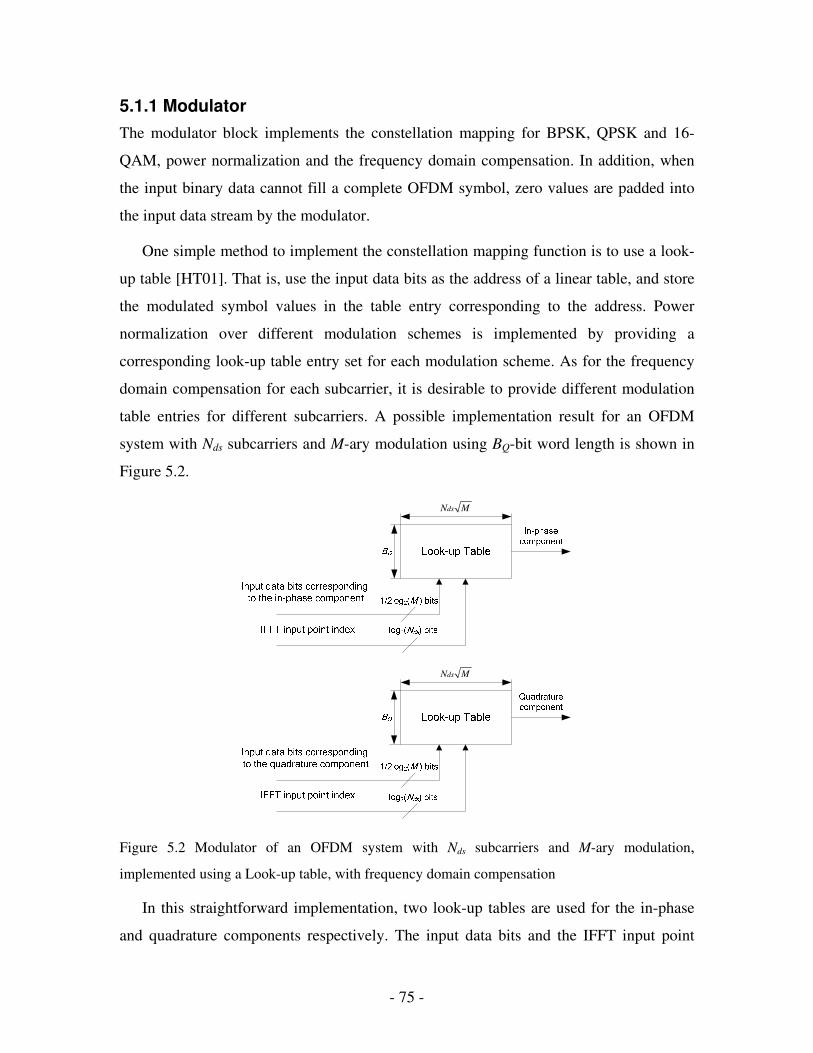
The application of OFDM technology to radios operating in the 60 GHz band has stimulated

much interest in the research community. The implementation of these systems has brought a

series of design challenges since a successful design must traverse multiple design

representation layers and experience numerous transformations. This thesis focuses on the

implementation of an OFDM baseband processing system for 60 GHz radios supporting data

rates of up to 1.5 Gbps. It covers the system level, architectural level and implementation

level design issues. A framework for OFDM system level design, including the identification

of key design parameters, a design tool to rapidly explore the design space, and an SoC-

oriented system functional model, has been proposed and implemented. A systematic finite-

word-length effect evaluation method based on statistical analysis and bit-true simulation has

been adopted to transform the algorithm into an area-efficient fixed-point implementation.

Architectures for critical building blocks are carefully explored to meet the required

performance specifications with acceptable cost. The whole system has been coded in

Verilog, verified, synthesized and implemented in a Xilinx FPGA.

Acknowledgements

I would like to thank my advisor Professor Glenn Gulak for his guidance, encouragement and

support throughout the course of this research. He has taught me many things that will

continue to guide me in the future.

Thanks to Dr. Javad Omidi for his advice, encouragement and all the detailed discussions.

I would not have been able to understand the OFDM theory so thoroughly without his help.

I would like to take the opportunity to thank Professor Paul Chow for lending me the Xilinx

FGPA board, without which this research would not have been possible.

Thanks to my fellow graduate-students for their friendship and help. Also, thanks to Jaro

Pristupa and Eugenia Distefano for their help and hard work to maintain the computer

systems.

I wish to express my gratitude to my parents and brothers for their support and love.

Finally, I would like to thank my wife Stella for her love, support, understanding and

patience.

- IV - IV

Table of Contents List of Figures ................................................................................................................... VI

List of Tables ..................................................................................................................VIII

List of Symbols ................................................................................................................. IX

List of Acronyms .............................................................................................................. XI

1. Introduction..................................................................................................................... 1

1.1 Motivation................................................................................................................. 1

1.2 Objectives ................................................................................................................. 2

1.3 Thesis Outline ........................................................................................................... 3

2. OFDM System ................................................................................................................ 4

2.1 From Single Carrier Modulation to Multicarrier Modulation................................... 4

2.2 OFDM Basics............................................................................................................ 8

2.2.1 Usage of DFT/IDFT........................................................................................... 9

2.2.2 Usage of GI ...................................................................................................... 12

2.3 A Practical OFDM System ..................................................................................... 15

2.3.1 Time domain windowing ................................................................................. 17

2.3.2 PAPR adjusting................................................................................................ 19

2.3.3 Frequency domain compensation .................................................................... 21

2.3.4 Frequency domain correction .......................................................................... 23

2.4 OFDM Standard...................................................................................................... 24

3. System-Level Design .................................................................................................... 27

3.1 Design Challenges and Proposed Solution ............................................................. 27

3.2 OFDM Calculator ................................................................................................... 30

3.2.1 Data rate and spectral efficiency calculation ................................................... 31

3.2.2 Filter sharpness requirement ............................................................................ 33

3.2.3 BER estimate ................................................................................................... 36

3.2.4 Link Budget calculation................................................................................... 37

3.3 Proposed 60 GHz System ....................................................................................... 40

3.3.1 Channel model ................................................................................................. 40

3.3.2 Design results................................................................................................... 42

4. Architectural Level Design ........................................................................................... 45

4.1 Design Challenges and Proposed Solution ............................................................. 45

4.2 Overview of the Design .......................................................................................... 47

4.3 FFT/IFFT Block...................................................................................................... 49

4.3.1 Fixed-point model transformation of the FFT/IFFT block .............................. 51

4.3.2 Architecture of the FFT/IFFT block ................................................................ 62

- V - V

5. Implementation Results ................................................................................................ 73

5.1 Implementation Specification ................................................................................. 73

5.1.1 Modulator......................................................................................................... 75

5.1.2 IFFT/FFT ......................................................................................................... 77

5.1.3 Framer .............................................................................................................. 83

5.1.4 Deframer .......................................................................................................... 84

5.1.5 Demodulator .................................................................................................... 85

5.2 Logic Level and Physical Level Design Flow ........................................................ 86

5.3 Verification and Validation..................................................................................... 87

5.3.1 Verification ...................................................................................................... 87

5.3.2 FPGA validation .............................................................................................. 89

5.4 Possibility of Standard-cell based Implementation................................................. 90

5.4.1 Standard-cell equivalence of the FPGA macros .............................................. 91

5.4.2 DFT in the ASIC.............................................................................................. 91

5.4.3 Preliminary standard-cell implementation results for the IFFT/FFT block..... 92

6. Conclusions................................................................................................................... 94

6.1 Summary ................................................................................................................. 94

6.2 Future Directions .................................................................................................... 95

A. A Comparison of OFDM Standards............................................................................. 98

B. Previous Research on Finite Word-length Effects of the FFT ................................... 101

C. Performance Simulation Results ................................................................................ 107

D. Inter-block Interface Timing...................................................................................... 109

E. Modulator Block Implementation Alternatives.......................................................... 110

F. Design Features and Verification Considerations ...................................................... 114

References....................................................................................................................... 120

- VI - VI

List of Figures

Figure 2.1 Block diagram of a digital communication system ........................................... 5

Figure 2.2 Effect of frequency selective channel on single carrier and multicarrier

systems. ............................................................................................................................... 6

Figure 2.3 Spectra of OFDM subcarriers............................................................................ 8

Figure 2.4 Discrete-time equivalent block diagram of DFT/IDFT based OFDM .............. 8

Figure 2.5 The sum of modulated subcarriers as the mega-symbol ................................. 11

Figure 2.6 Generation of GI.............................................................................................. 12

Figure 2.7 Benefit of cyclic prefix.................................................................................... 14

Figure 2.8 Functional Block diagram of an OFDM SoC.................................................. 15

Figure 2.9 Time domain windowing................................................................................. 18

Figure 2.10 Implementation of DAC ................................................................................ 21

Figure 2.11 Amplitude response of the zero-order hold ................................................... 22

Figure 3.1 Key parameters of an OFDM system and their relationship ........................... 29

Figure 3.2 Two-step system-level design approach.......................................................... 30

Figure 3.3 Filter sharpness requirement............................................................................ 34

Figure 3.4 Link budget model........................................................................................... 37

Figure 3.5 Relationships among the parameters ............................................................... 39

Figure 4.1 Architectural level design flow ....................................................................... 46

Figure 4.2 Architectural block diagram of the proposed system...................................... 48

Figure 4.3 16-point radix-4 DIF FFT SFG ....................................................................... 50

Figure 4.4 Butterfly of radix-4 DIF FFT .......................................................................... 50

Figure 4.5 DAC/ADC quantization model with clipping noise and rounding noise ........ 55

Figure 4.6 Proposed noise analysis model........................................................................ 57

Figure 4.7 Projection of SFG into PEs.............................................................................. 63

Figure 4.8 Projection of the crossadder ............................................................................ 67

Figure 4.9 SDF architecture for a 16-point radix-4 FFT .................................................. 69

Figure 4.10 SDC architecture for a 16-point FFT............................................................. 70

Figure 4.11 R4MDC architecture for an example of 64-point DIF FFT .......................... 71

Figure 5.1 The Baseband Modulation/Demodulation Core.............................................. 73

Figure 5.2 Modulator of an OFDM system with Nds subcarriers and M-ary modulation. 75

Figure 5.3 Quantization of compensation function........................................................... 76

Figure 5.4 Modulator implementation .............................................................................. 77

Figure 5.5 IFFT/FFT implementation............................................................................... 78

Figure 5.6 ISQ implementation......................................................................................... 79

Figure 5.7 STG module implementation for stage 3 (STG3) ........................................... 80

Figure 5.8 Pipelined and retimed STG module implementation for stage 3 (STG3) ....... 82

Figure 5.9 OSQ implementation ....................................................................................... 83

Figure 5.10 Framer implementation ................................................................................. 84

Figure 5.11 Demodulator implementation........................................................................ 85

Figure 5.12 Logic level and physical level design flow ................................................... 86

- VII - VII

Figure 5.13 On-board validation....................................................................................... 89

Figure B.1 Classic noise model for radix-2 DIT FFT..................................................... 101

Figure B.2 Improved noise propagation model .............................................................. 104

Figure B.3 Detailed noise analysis model for a radix-2 butterfly................................... 105

Figure C.1 Equivalent SNR under multi-path channel with τrms=9ns, for 16-QAM. ..... 107

Figure C.2 BER under multi-path channel with τrms=9ns, for 16-QAM......................... 108

Figure D.1 Inter-block interface timing for the transmitter mode .................................. 109

Figure D.2 Inter-block interface timing for the receiver mode....................................... 109

Figure E.1 Frequency domain compensation by multiplication ..................................... 111

Figure E.2 Straight-line approximation of the compensation function........................... 112

Figure E.3 Architecture to implement the approximation .............................................. 112

- VIII - VIII

List of Tables

Table 3.1 Proposed 60 GHz OFDM System..................................................................... 42

Table 4.1 Signal-to-rounding-noise ratio with ideal IFFT/FFT........................................ 56

Table 4.2 Simulation results of equivalent SNR............................................................... 61

Table 4.3 Implementation architectures for an N-point FFT with Fs Samples/s .............. 65

Table 4.4 Implementation architectures for a 1024-point FFT with 512 MSamples/s ..... 65

Table 4.5 Comparison of cascade FFT architecture ......................................................... 72

Table 5.1 Twiddle factor memory requirement ................................................................ 81

Table 5.2 Delay elements requirement ............................................................................. 81

Table 5.3 Standard cell implementation result for the IFFT/FFT block........................... 93

Table A.1 Comparison of OFDM standards and the proposed 60 GHz system............... 99

Table A.2 60 GHz OFDM Comparison.......................................................................... 100

- IX - IX

List of Symbols

t Time for continuous-time signal in seconds

ω Angular frequency in radians/second

h(t) Impulse response of a channel

H(jω) Frequency response of a channel

τ Delay time in seconds

n Index of a time-domain sequence

k Index of a frequency-domain sequence

N General FFT size

Na Number of altered samples at either the head or the tail of an OFDM

symbol due to the time-domain windowing

Ngi GI length in number of samples

No Number of samples overlapping with adjacent symbol at either the head

or the tail of an OFDM symbol

Nes Number of samples in an OFDM mega-symbol

Bch Channel bandwidth in Hertz

Fs Sampling frequency in Hertz

γ Sampling factor

NFFT Size of the FFT used in an OFDM system

Nsc Number of subcarriers used

Nds Number of data subcarriers used

β Nds to NFFT ratio

Nps Number of pilot and signaling subcarriers

δ Nps to NFFT ratio

Ndn Number of DC & notch subcarriers

θ Ndn to NFFT ratio

Ts Sample period in seconds

Tus Un-extended symbol length in seconds

Tgi GI length in seconds

α Tgi to Tus ratio

Tes Extended symbol length in seconds

- X - X

Fss Subcarrier spacing in Hertz

Bsc Major energy bandwidth in Hertz

ς Filter sharpness factor

DRraw Max. uncoded data rate in bits/second

DR Max. data rate in bits/second

σ Variance of a random process or random variable

η Spectral efficiency in bits/second/Hertz

W Base of the twiddle factors

- XI - XI

List of Acronyms

ADC Analog-to-Digital Converter

AGC Automatic Gain Control

ASIC Application Specific Integrated Circuit

ATPG Automatic Test Pattern Generation

AWGN Additive White Gaussian Noise

BER Bit Error Rate

BIST Built-In Self Test

BO Butterfly Operation

BPSK Binary Phase-Shift Keying

CA Cross Adder

CCT Compensation Coefficient Table

CIR Channel Impulse Response

CLB Configurable Logic Block

COM COMmutator

DFT Discrete Fourier Transform, or Design For Testability

DAC Digital-to-Analog Converter

DCM Digital Clock Manager

DIF Decimation-In-Frequency

DIT Decimation-In-Time

DVB-H Digital Video Broadcast –Handheld

DVB-T Digital Video Broadcast –Terrestrial

EDA Electronic Design Automation

ENOB Effective Number Of Bits

FDCT Frequency Domain Correction Table

FEC Forward Error Correction

FFT Fast Fourier Transform

FIFO First-In, First-Out

FO4 Fanout Of 4

GI Guard Interval

GWE Gigabit Wireless Ethernet

- XII - XII

HDTV High Definition TV

IDFT Inverse Discrete Fourier Transform

IFFT Inverse Fast Fourier Transform

ICI Inter-Carrier-Interference

IP Intellectual Property

ISI Inter-Symbol Interference

ISQ Input SeQuencer

ISVT In-phase Symbol Value Table

LOS Line-Of-Sight

LUT Look-Up Table

MCM MultiCarrier Modulation

MDC Multi-path Delay Commutator

MMSE Minimum Mean Square Error

MPEG Moving Picture Experts Group

m-QAM m-array Quadrature Amplitude Modulation

NLOS Non-Line-Of-Sight

OFDM Orthogonal Frequency Division Multiplexing

OSQ Output SeQuencer

PAN Personal Area Network

PAPR Peak-to-Average Power Ratio

P&R Place And Route

PDU Payload Data Unit

PE Processing Element

PLL Phase Lock Loop

PSCT Pulse Shaping Coefficient Table

QPSK Quadrature Phase-Shift Keying

QSVT Quadrature Symbol Value Table

RCT Read ConTrol

RM Reference Model

RMS Rooted Mean Square

RS Reed-Solomon

RTL Register Transfer Level

- XIII - XIII

SDC Single-path Delay Commutator

SDF Single-path Delay Feedback

SDTV Standard Definition TV

SFG Signal Flow Graph

SNR Signal-to-Noise Ratio

SoC System-on-a-Chip

SOW Start Of a Window

SBT Segment Boundary Table

SVT Step Value Table

TFM Twiddle Factor Memory

UCF User Constraints Files

UWB Ultra-WideBand

WCT Write ConTrol

WIGWAM WIreless Gigabit With Advanced Multimedia

ZF Zero Forcing

ZOH Zero-Order-Hold

- 1 -

1. Introduction

1.1 Motivation

The past decade has witnessed the exploding development of the Internet and digital

multimedia. Recently the demand for “anywhere” multimedia applications, such as

Gigabit Wireless Ethernet (GWE) and high-speed connections for uncompressed HDTV-

quality signals between displays and miscellaneous video sources, has spurred

considerable interest in the design and implementation of high speed wireless networks

with data rates of up to Gbps. For instance, the WIGWAM project (Wireless Gigabit with

Advanced Multimedia), a collaboration of 27 research partners, is aimed at designing a

1 Gbps system for the home/office, public access and high velocity scenarios [FI05]; the

802.15.3a working group has proposed an ultra-wideband (UWB) system to provide a

wireless PAN (Personal Area Network) with data-rates of up to 1.32 Gbps [PAN04].

Huge bandwidth requirements and high data processing throughputs have presented many

system implementation challenges.

An OFDM (Orthogonal Frequency Division Multiplexing) based system proposed in

this thesis, operating at 60 GHz with data-rates of up to 1.6 Gbps, is a promising solution

for these types of networks. The FCC has assigned the 59-64 GHz frequency band for

unlicensed wireless communications [FCC98]. In addition to the huge bandwidth,

wireless channels at 60 GHz exhibits large attenuation of 10 – 15 dB/km due to oxygen

absorption and that makes frequency re-use easier [Smu02]. However, a wide-band

channel also means higher probability of severe frequency selectivity, the major obstacle

that traditional single carrier modulation systems have been struggling to overcome.

Fortunately, OFDM is an appealing technology to combat this channel impairment, and

its relatively simple implementation based on FFT (Fast Fourier Transform) makes the

solution feasible and cost-effective.

A fully functional OFDM communication system incorporates high-performance RF

components, complex signal processing algorithms and enormous hardware/software

cooperation. Based on increasing capability for device integration in silicon, a System-

on-a-Chip (SoC) approach provides the benefits of integrating a large number of

- 2 -

functional units, yielding a cost effective implementation approach for our proposed

OFDM system. On the other hand, SoC design has created great challenges for the design

community. For instance, with such a large number of devices and the time-to-market

pressure, timing closure and functional verification are two dominant problems [KB02].

A remedy to the problems is to have high quality, reusable Intellectual Property (IP) for

most of the SoC system, and leave the major design task at the system level as the

integration of the IPs. Thus the success of a SoC solution depends heavily on the

availability and quality of the IP cores. For our proposed OFDM system, high quality IP

cores are especially important due to the high performance requirements of the system.

Yet it is challenging to design the needed IP cores. The following aspects require careful

consideration:

An ideal design requires a thorough understanding of relevant communication

theory and the adoption of appropriate algorithms and design parameters. OFDM

theory, due to its nature, is more complicated than single carrier communication theory.

There exist many interrelationships among the related aspects and design parameters of

the system. Algorithm choice and parameter trade-offs will affect not only the final

performance of the system, but also the implementation cost and complexity;

Good architectures are very important for the high performance targets. Even if

excellent algorithms could be proposed, to meet the high throughput requirements,

reasonable trade-offs among timing, area and power have to be carefully made;

A systematic, highly productive design methodology is the key for the timely

progress of the design. Since the IP cores must evolve from concept to algorithms, then

to architectures and eventually to silicon, considerable transformations of design

representations exist and so do many chances for errors. How to efficiently express the

design idea, thoroughly explore the design space, quickly yet accurately transform the

design forms, and effectively verify the design, are heavily relying on the design

methodology, i.e. principles, tools, techniques and flows.

1.2 Objectives

As mentioned above, the mission of designing IP cores for the proposed OFDM system

involves multi-disciplinary tasks, multi-trade-offs, and a series of design challenges

- 3 -

during different design phases. The research presented in this thesis has been carried out

with the following objectives:

• To address key design issues of the core baseband functionality for the 60 GHz

Radio;

• To provide fully functional building blocks for the principle components of the

OFDM engine;

• To experiment and summarize a systematic design methodology.

It is desirable to build a complete working system. However, due to the complexity of the

OFDM system and available time and resource, only the modulation and demodulation

core blocks are covered in the research, while other important blocks such as channel

estimation and synchronization have to be excluded. It is also tempting to tackle the

OFDM SoC design problem as a whole subject, but unfortunately the overall problem of

OFDM SoC is beyond the scope of the thesis, although the thesis research has been

carried out bearing the SoC in mind and relevant information will be discussed wherever

appropriate.

1.3 Thesis Outline

This thesis is organized as follows. In Chapter 2, the basic fundamentals of OFDM will

be introduced, followed by a discussion of practical OFDM system implementation

considerations, and then concluded by a brief introduction to four OFDM international

standards. Chapter 3 will focus on system level design, revealing the intricate

interrelationships among the design parameters, and the proposed OFDM baseband

design for 60 GHz radios will be elaborated. In Chapter 4, the architecture of proposed

system will be discussed, with the emphasis on the most important block, the FFT/IFFT

block. Chapter 5 will report the implementation results of the system and Chapter 6 will

conclude the thesis with a summary and future research directions.

- 4 -

2. OFDM System

This chapter provides an overview of the basic ideas behind OFDM (Orthogonal

Frequency Division Multiplexing) technology. It starts with a discussion of the

limitations of single-carrier systems to achieve high data rates in frequency selective

channels, and then proceeds to introduce the solution provided by multi-carrier systems,

focusing on the basic theory of OFDM, the usage of IDFT (Inverse Discrete Fourier

Transform)/DFT (Discrete Fourier Transform) and Guard Intervals (GI). IDFT/DFT is

used to implement the modulation and demodulation onto the basic orthogonal

subcarriers, while GI tries to guarantee that the orthogonality among the subcarriers will

not be altered so that no Inter-Symbol Interference (ISI) or Inter-Carrier Interference (ICI)

would occur. Following that, additional functional blocks to implement the OFDM

modulation core and demodulation core are elaborated, including time domain

windowing and frequency domain compensation and correction. These functional blocks

are needed to shape the spectrum of the OFDM signal and improve the system

performance. To end this chapter, the features of four OFDM-based international

standards are introduced.

2.1 From Single Carrier Modulation to Multicarrier Modulation

A digital communication system consists of a transmitter, a receiver and a channel, as

shown in Figure 2.1. In a single carrier modulation system, data symbols are modulated

on a single carrier, i.e. the spectrum of the baseband equivalent signal is shifted to the

passband centered on one single carrier frequency. It is desirable for any digital

communication system to achieve the required data rate with acceptable BER under the

constraints of a given signal bandwidth and signal power, while the implementation

should have reasonable complexity and cost. However, as explained below, it is not easy

for single carrier modulation systems to achieve this under certain circumstances.

In any digital communication system, there are two major impairments applied to the

signal when it traverses from the transmitter via the channel to the receiver: linear

distortion and additive noise. Linear distortion is caused by the “memory effect”

introduced by the channel, such as multi-paths existing in wireless communication

- 5 -

channels, or reflections of un-appropriately terminated cables in fixed-wire

communication scenarios, while noise could be caused by different sources such as

thermal movement of the electrons of the receiver front-end, energy leaked from

neighbouring channels, and so on. As shown in Figure 2.1, the transmitted signal, s(t),

will convolve with the channel impulse response (CIR), h(t), and the result of the

convolution will be added with the noise, n(t), resulting in the received signal r(t) at the

receiver:

r(t) = s(t) * h(t) + n(t). (2.1)

Transmitter ReceiverLinear

Distortation( )

+

Noise ( )Channel

( )( )

Figure 2.1 Block diagram of a digital communication system

In the following section, we will focus on the linear distortions, whose effect on a

digital communication system could be demonstrated in either the time domain or the

frequency domain. In the time domain, ideally h(t) should be an impulse, but due to the

memory effect mentioned above, in most cases it is a dispersive signal with a

considerable length before attenuating to zero. After s(t) convolves with h(t), ISI will be

introduced at the receiver side since any transmitted symbol will be extended by the

dispersive CIR and intrude into successive symbol(s). The length of the dispersion

determines the severity of the ISI and when the ISI is comparable to the length of the

symbol, the quality of the transmission is severely degraded. In the frequency domain, the

frequency response of the above-mentioned channel, H(jω), is not flat, but has deep fades

in certain frequency bands, i.e. a frequency selective channel, as depicted in Figure 2.2(a).

Even if the fades correspond to only a portion of the transmitted signal spectrum, the

transmission is degraded, as the received signal’s spectrum illustrates in Figure 2.2(b).

- 6 -

ω

(a)

ω

(b)

ω

Guard bands

(c)

Figure 2.2 Effect of frequency selective channel on single carrier and multicarrier systems. (a)

Amplitude response of the channel; (b) Effect on a single carrier system; (c) Effect on a

multicarrier system

To combat the degradation, an equalizer could be adopted in the receiver to shape the

CIR toward an ideal impulse, or as its name implies, to “equalize” the frequency response

and make it flat. However, the implementation cost of the equalizer is high; besides,

- 7 -

when the equalizer tries to boost attenuated frequency components, noise is also

amplified and the overall performance shows diminishing improvement.

For single carrier systems to reach high data rates, shorter symbol length must be

adopted and unfortunately the dispersion of the channel will have greater effect, therefore

the performance will become worse.

A solution is to use MultiCarrier Modulation (MCM): divide the wide-band required

by the high data rate into many (say, N) narrow-band sub-channels and transmit

information in these sub-channels simultaneously by modulating the data stream on N

corresponding subcarriers. In the time domain, for each subcarrier modulation, the

symbol period is much larger than otherwise required by a single carrier modulation, so

the effect of ISI can be mitigated. An additional benefit of the longer symbol length is

that the impulse noise existing in certain channels will do less harm to the MCM than to

the single carrier modulation systems [Bin90]. In the frequency domain, there are two

benefits associated with MCM: since the deep fades of the channel correspond to limited

number of sub-channels, only those sub-channels will be affected, as shown in Figure

2.2(c). An adaptive modulation scheme could even be adopted to exploit this fact, e.g.

avoiding transmitting in these sub-channels. Another benefit is, because the frequency

band corresponding to a particular sub-channel could be regarded as a flat channel,

equalization could be achieved using a one term complex number multiplication, as will

be discussed later.

However, for this simple form of MCM, in order to prevent interference between

adjacent subcarriers, i.e. ICI, guard bands must be introduced, as in Figure 2.2(c), so the

spectral efficiency is lower than that of a single carrier system. It is desirable to have a

“compact” MCM system where the spectrum of the subcarriers could be overlapping with

each other yet it is still possible to separate them in the receiver side. OFDM is such a

system where the spectrums of the sub-channels are orthogonally overlapping with each

other, as shown in Figure 2.3. The detail of this Figure and other intricate concepts of

OFDM will be discussed next.

- 8 -

Figure 2.3 Spectra of OFDM subcarriers

2.2 OFDM Basics

The initial concept of OFDM was proposed in the 1960s [CG68]. However, the

complexity of this idea had kept it from being implemented until 1971 when Weinstein

and Ebert proposed to use IDFT and DFT to generate the orthogonal subcarriers in the

baseband [WE71].

Figure 2.4 Discrete-time equivalent block diagram of DFT/IDFT based OFDM

The discrete-time equivalent block diagram of this IDFT/DFT based OFDM system is

shown in Figure 2.4. At the transmitter side, the input binary data stream is mapped into

data symbols using an amplitude and/or phase modulation scheme such as BPSK, QPSK

Serial

to

Parallel

X0

XN-1

x0

xN-1

IDFT Add GI

Parallel

to

Serial

X0

XN-1

x0

xN-1

DFT Remove GI

Serial

to

Parallel

Channel

.

.

.

.

.

.

.

.

.

.

.

.

Input Data

Output Data

Constellation

Mapping

Constellation

Demapping

Parallel

to

Serial

- 9 -

and m-QAM. The data symbol stream is divided by a serial-to-parallel converter into N

parallel sub-streams, each corresponding to a subcarrier. An IDFT is applied to a

frequency domain sequence consisting of N data symbols X0, X1, …, XN-1, one from every

sub-stream, to transform the sequence into a time domain sequence x0, x1, …, xN-1. The

sequence is converted back to serial form, and a cyclic prefix is added to the sequence as

a guard interval (GI) to eliminate ISI and ICI (as explained in section 2.2.2). A reverse

procedure happens in the receiver side: the time-domain sequence x0, x1, …, xN-1 is

retrieved from the received data stream, then transformed back to the frequency domain

sequence X0, X1, …, XN-1 by a DFT, and finally demapped into the original binary data

stream.

The most important idea here is the usage of the DFT/IDFT and the GI, as described

below.

2.2.1 Usage of DFT/IDFT

The IDFT is used to modulate the parallel sub data streams onto N subcarriers with equal

distance away from each other in the frequency spectrum, and at the same time achieve

orthogonality among the subcarriers. As well-known, the IDFT is defined as:

21

0

1[ ] [ ]

=

= ∑j nkN

N

k

x n X k eN

π

n = 0, 1, …, N-1. (2.2)

Its continuous time counterpart could be written as

21

0

1( ) [ ]

=

= ∑ s

j ktNNT

k

x t X k eN

π

0 ≤ ≤s

t NT , (2.3)

where Ts is the sampling period of the discrete system. It is revealing to interpret (2.3) as

the sum of N complex modulated signals, each of which is generated by modulating one

complex symbol X[k] with rectangular pulse shaping onto a complex subcarrier

2

s

j kt

NTe

π

, or

in other words, to modulate the in-phase and quadrature components of X[K] into

2cos

s

kt

NT

πand

2sin

s

kt

NT

πrespectively. All the subcarriers are orthogonal to each other,

since for any two subcarriers sk(t) and sm(t),

- 10 -

2 2

*

0

( ) ( )0

−∞

−∞

= = =

≠∫ ∫

S

s s

j kt j mtNT

SNT NT

k m

NT k ms t s t dt e e dt

k m

π π

. (2.4)

Since each modulated subcarrier in (2.3) contains the information of a data symbol,

the sum itself is named a mega-symbol. Figure 2.5 shows an example of how the

modulated subcarriers add up to generate one mega-symbol. A QPSK modulation scheme

has been assumed and only the quadrature component is displayed. The orthogonalites

could be demonstrated as that during the symbol time of length NTs, every subcarrier has

an integer number of cycles, while adjacent subcarriers differ with each other by exactly

one cycle.

The orthogonalities could also be checked in Figure 2.3, where the spectrum of each

subcarrier goes to zero at the points corresponding to the maxima of every other

subcarrier1, thus at the receiver side it is possible to obtain those maxima values without

interference from other sub-channels, i.e. without ICI. To achieve this, the DFT is used as

a reverse procedure of the IDFT; In addition, there must be no carrier or timing recovery

error in the receiver side, so that the DFT could be carried out at the centers of the

subcarriers.

A third viewpoint to interpret the orthogonality is that the Nyquist Criterion is met in

the frequency domain, and no ICI should exist if we can sample the information at

exactly the center of each subcarrier [HMC03].

1 Why the spectrum is like this will be discussed in section 2.3.

- 11 -

...

1 ( )

2 ( )

3 ( )

4 ( )

1

( )=

∑N

i

i

S t

Figure 2.5 The sum of modulated subcarriers as the mega-symbol

- 12 -

2.2.2 Usage of GI

A cyclic prefix GI is generated by copying the last Ngi (Ngi ≤N) samples of the original

mega-symbol and attaching them to the beginning of the original mega-symbol, as shown

in Figure 2.6. In this thesis, the original mega-symbol is also named “un-extended mega-

symbol” or “un-extended symbol” where the distinction is necessary.

Figure 2.6 Generation of GI

The GI is used to further reduce ISI and avoid ICI. How that is achieved will be

described next. It might be argued that by using multiple subcarriers, the length of ISI is

so trivial compared with the length of the symbol that ISI will have no effect on detection,

just as in a single carrier system. However, the demodulation of OFDM is completely

different from that of a single carrier system: in order to determine the original data

symbol value, the DFT is carried out on every data sample within the DFT window to

calculate the frequency content of each subcarrier. So if ISI is longer than a sample, it

will affect the detection. The effect of GI can be observed in the time domain by checking

the waveform of one transmitted subcarrier. In the time domain, the convolution of a

dispersive CIR with a modulated subcarrier is the sum of a series of subcarriers with the

same frequency but different amplitudes and delays due to the multiple terms of the CIR.

To illustrate the effect of the channel, Figure 2.7(a) shows the quadrature components of

two extreme subcarriers, the ones with the minimum delay and the maximum delay

respectively, for two consecutive symbol periods. It is obvious there is one phase shift on

one of the waves within the receiver side DFT window. The DFT will detect the

information leaked from the first symbol into the second symbol marked by this phase

transition. It is possible to insert a guard interval consisting of zero values to eliminate ISI,

as in Figure 2.7(b). However, there is still a sudden waveform change inside the DFT

window, and it generates higher spectrum components that will be detected by the DFT

Original mega-symbol Cyclically-extended mega-symbol

- 13 -

as ICI. A cyclic prefix, as depicted in Figure 2.7(c), will guarantee there is no phase

change within the DFT window and every sine wave has an integer number of cycles

within the DFT window, so that no ISI or ICI will occur.

Another viewpoint to understand the GI is from the perspective of discrete-time signal

processing: the cyclic prefix transfers the linear convolution of the transmitted signal with

CIR into a cyclic convolution. This is equivalent to a scalar multiplication in the

frequency domain and so the orthogonality will be maintained [Eng02].

We also need to keep in mind that the orthogonality could be kept only when the

dispersion of the channel is shorter than the GI, and there is no carrier or timing error.

Thus the longer the GI, the more robust the system is against channel dispersion. On the

other hand, a longer GI means more overhead. The strategy of choosing the GI length

will be discussed in Chapter 3, and next we need to first have a look at the whole picture

in the context of a practical OFDM SoC implementation.

- 14 -

( -1)th symbol th symbol

a)

DFT window

( -1)th symbol th symbol

b)

DFT window

( -1)th symbol th symbol

c)

DFT window

GI

GI

Waveform with min. delay

Waveform with max. delay

Waveform with max. delay

Waveform with min. delay

Waveform with min. delay

Waveform with max. delay

Figure 2.7 Benefit of cyclic prefix [HP03] (a) OFDM without guard interval; (b) OFDM

with zero guard interval; (c) OFDM with cyclic prefix guard interval.

- 15 -

2.3 A Practical OFDM System

Figure 2.8 Functional Block diagram of an OFDM SoC

Additional functional blocks beyond those shown in Figure 2.4 are needed to implement

a functioning OFDM SoC, as shown in Figure 2.8. Generally the system can be divided

into the baseband processing part and RF/IF part. The functions of each block are briefly

summarized below.

At the transmitter side, a FEC Encoder provides channel coding for the input data, to

lower the Bit Error Rate (BER) of the system with the cost of certain overhead. The

encoded data is modulated in the modulation core, which contains the following blocks:

Constellation Mapping: map the encoded binary data into complex symbol value

based on the adopted modulation scheme.

Frequency Domain Processing: normalizes the amplitude of the complex values

such that all modulation schemes have similar average power, and compensates the

Zero-Order-Hold (ZOH) effect of the DAC or other defects of the analog system by

multiplying the complex values in the frequency domain with an appropriate

compensation function.

IFFT: Inverse Fast Fourier Transform, a fast algorithm to calculate the IDFT,

transforming each data symbol from the frequency domain into the time domain.

Data out

FEC

Encoder

Constellation

Mapping

Time Domain

Processing

FEC

Decoder

Constellation

Demapping

Freq. Domain

Correction

Frame

Synchronization

Freq. Domain

Processing

Channel Estimation

FFT

Modulation Core

DAC

Channel

Demodulation Core

Analog

Front-end

ADC Analog

Front-end

IFFT

Frequency & Timing

Synchronization

Data in

Baseband Processing RF/IF

- 16 -

Time Domain Processing: inserts the GI, multiplies the time domain values with a

certain window function to help shape the transmitted signal spectrum, and adjusts

the PAPR (Peak-to-Average Power Ratio) 2 to an acceptable level.

The modulated OFDM baseband signal, x(t) as shown in equation (2.3), is a complex

signal, and the transmitted RF signal3 is

2( ) Re{ ( ) } ( )cos(2 ) ( )sin(2 )= = −cj F tre c im cs t x t e x t F t x t F t

π π π , (2.5)

where Re{} represents the operation to take the real part of a complex signal, while xre(t)

and xim(t) are the real and imaginary parts of x(t) respectively. So one way to generate the

RF signal is to use two DACs to generate xre(t) and xim(t), up-converted to the carrier

frequency and mixed to generate s(t) following (2.5). The RF signal is then amplified and

transmitted by the analog front-end.

At the receiver side, the received signal is down-converted, separated into in-phase

and quadrature components and then sampled by two ADCs. The digital samples are

demodulated by the demodulation core, which contains the following sub-blocks.

Frame Synchronization: identifies each data symbol, and allocates the FFT

window location under the control of the timing synchronization block, as discussed

later.

FFT: Fast Fourier Transform, a fast algorithm to calculate the IDFT, transforming

each data symbol from the time domain into the frequency domain.

Frequency Domain Correction: corrects the linear amplitude and phase distortion

of the channel by multiplying the complex symbol value of each sub-channel with

one complex coefficient corresponding to the frequency response of that particular

sub-channel provided by the channel estimation block.

Constellation Demapping: demaps the corrected data symbol to restore the binary

data.

The demodulated data is then fed to the FEC Decoder for generating the original un-

coded data. Meanwhile, the frequency and timing synchronization block provides

important timing information: It works with the analog front-end to recover an accurate

2 Also written as PAR in some research literature. 3 In wireline OFDM system such as HomePlug [LNL03], baseband signal is directly transmitted. One way

to generate such a signal is to make the input signal of the IFFT complex conjugate, and then the output is a

real signal that can be transmitted directly.

- 17 -

carrier frequency so that the signal could be correctly down-converted to the baseband; It

also adjusts the sampling clock for the ADC and so there is no frequency shift that may

cause additional ICI [FK03]; Finally it helps to allocate the FFT window location, such

that within the FFT window, there is no phase shift of the subcarriers, and so there is no

ICI, as discussed before.

As stated earlier, this thesis will focus on the modulation core and the demodulation

core, to this end the following discussion will focus on those blocks. One obvious

question is why the practical implementation needs the “additional” blocks presented in

Figure 2.8, compared with Figure 2.4. A short answer is to shape the OFDM signal

generated by the simple method in Figure 2.4 in the time domain and the frequency

domain, such that the constraints imposed by the operating environment and the

feasibility of implementation could be met, while achieving the performance goal. In the

following sections, the time domain processing and the frequency domain processing

functions will be further discussed.

2.3.1 Time domain windowing

Time domain windowing is performed to help shape the spectrum of the transmitted

signal. To understand this, we need to first check the spectrum of the simple OFDM

signal as generated in Figure 2.4, which has the famous side-lobe problem due to the

rectangular pulse shaping, and the un-desired high frequency components caused by the

sharp phase transition at the OFDM symbol boundaries, as explained below.

When we discuss the “spectrum” of the OFDM signal, we need to be careful which

section of the signal is referred to – the un-extended mega-symbol, or the signal

consisting of many extended symbols – and where the observation point is. Figure 2.3 is

often claimed to be the spectrum of OFDM signals, as stated in some of the literature

about OFDM, for example [NP00]. Strictly speaking it is only the spectrum of an un-

extended symbol, or in other words, the spectrum “detectable” by the FFT in the receiver

side. This part of the signal is generated by using the IFFT, so according to the definition

of IDFT, if this section of the signal is duplicated to generate a periodic signal,

21'

0

( ) [ ]−

=

=∑ s

j ktNNT

k

x t X k e

π

−∞ < < ∞t , (2.6)

- 18 -

then its spectrum is a series of Dirac pulses located at the subcarrier frequencies. Since an

un-extended symbol is only a cycle of (2.6), it could be imagined as the product of (2.6)

with a rectangular pulse with length of NTs. Thus its spectrum is the convolution of the

above-mentioned Dirac pulses with the spectrum of the rectangular pulse, a sinc function.

The convolution will be the sum of a series of shifted sinc functions with the same shape,

generating the spectrum in Figure 2.3. A sinc function has unlimited number of decaying

side-lobes, so the sum of the above mentioned sinc functions results in a slowly decreased

edge of the spectrum.

The spectrum of the actual transmitted signal will have a much less severe side-lobe

problem, since the signal is not an isolated symbol, and the reconstruction filter of the

DAC also helps to shape the spectrum. However, sharp phase transitions exist in the

symbol boundaries due to the rectangular pulse shaping, as in Figure 2.7, so high

frequency components will be generated and it will make the out-of-band spectrum

control more difficult [NP00]. Although guard subcarriers and the reconstruction filter of

the DAC are the major mechanisms to shape the final spectrum, it is still desirable to

have some improvement methods in the baseband processing. One such method is to

smooth the phase transition across symbol boundaries by multiplying the original symbol

with a window function. One possible implementation is shown in Figure 2.9: the first Na

and the last Na samples of each symbol are altered, at the same time adjacent symbols are

overlapped with each other over a region of No samples to further smooth the transition,

while Nm samples are un-changed. Please notice by doing this the nominal length of a

symbol, Nes, is No samples shorter than the original length, Noes.

Figure 2.9 Time domain windowing

- 19 -

One possible candidate for the window function is the raised cosine window Wrc[n],

defined as

0.5 0.5cos( / ) 0

[ ] 1.0

0.5 0.5cos(( ) / ) 2

+ + ≤ ≤

= ≤ ≤ + + − − + ≤ ≤ +

a a

rc a m a

m a a m a m a

n N n N

W n N n N N

n N N N N N n N N

π π

π

. (2.7)

Please note that the rising and falling edge of the window is relatively short. This will

make the implementation easy since only a small part of the symbol needs to be changed.

More importantly, by doing this, enough region of the symbol has been left unchanged

for maintaining the orthogonality between the subcarriers4. Some researchers have

proposed to use other window functions which have much longer rising and falling edges

so that the orthogonality is not maintained [Mol01]. This technique, known as “soft pulse

shaping”, has been claimed to have much better spectrum shape control and make OFDM

less prone to synchronization errors. This idea needs further scrutiny and will not be

adopted in the proposed system.

2.3.2 PAPR adjusting

A baseband OFDM signal is the sum of multiple modulated complex exponential

functions, and so its in-phase and quadrature components might add up to very large

values when the modulating data sequence has certain bits stream. In fact, consider the

definition of the IFFT as in equation (2.2):

21

0

1[ ] [ ]

=

= ∑j nkN

N

k

x n X k eN

π

n = 0, 1, …, N-1, (2.2)

where X[k] is the complex data symbol sequence. We can define the PAPR (Peak-to-

Average Power Ratio) of the OFDM signal in dB as:5

4 To maintain the orthogonality, the FFT window at the receiver side will not be at the same position as the

IFFT window in the transmitter side, but rather a few samples ahead. This will not be a problem, since once

the FFT is still inside a symbol, shifting the FFT window will only cause phase rotation that could be taken

into account by the frequency domain correction. In fact, FFT window will be shifted for synchronization

purposes anyway.

5This is a widely-adopted definition of PAPR (e.g. in [KMC05]). In some literature (e.g. [NP00]), the peak

power is defined as the power of a sine wave with an amplitude equal to the maximum envelope value of

the signal, and so an un-modulated carrier has a PAPR of 0 dB.

- 20 -

( )2

10 2

max ( )10log

E ( )=

x nPAPR

x n. (2.8)

Since the signal is zero-mean, the average power2

E ( )

x n in (2.8) is also the variance of

the signal.

Without loss of generality, assume the modulation scheme is 16-QAM with power-

normalized complex symbols of

1( 1 j)

10± ±

,

1( 1 3j)

10± ±

,

1( 3 j)

10± ±

,

1( 3 3j)

10± ±

,

then the in-phase and quadrature components of each modulated subcarrier are both

random processes with zero means and the same variance

2 1

2=SCσ . (2.9)

When the FFT size N is large, according to the central limit theorem, both the in-

phase and quadrature components of the OFDM signal are very close to a Gaussian

process with zero mean and variance

2

2

2

1

2= =

SCN

N N

σσ . (2.10)

So the amplitude of the OFDM signal has a Rayleigh distribution, and the PAPR can be

relatively high with certain probability. For instance, simulation in [NP00] shows that for

1024 subcarriers, the probability that a mega-symbol has a PAPR of less than 8 dB is

approximately 0.1. The high PAPR scenario requires higher DAC and ADC resolution

and larger RF front-end linearity range, so it must be adjusted to be kept within certain

levels.

This PAPR control problem has been a central topic in the OFDM research. [NP00]

systematically categorizes the proposed solutions as non-distortion and distortion

methods. The non-distortion method will not alter the “correct” sample values; rather it

adopts such approaches as PAPR reduction codes which only produce OFDM symbols

with PAPR below certain level, or multiple symbol scramblings where only the

scrambled result with the smallest PAPR is transmitted. The distortion method, as

- 21 -

implied by its name, would sacrifice the “correct” value for lower PAPR. Clipping is the

simplest distortion method which clips the signal amplitudes exceeding a certain

threshold. However, this method generates sharp signal changes and thus results in out-

of-band power radiation. To lower this radiation, other distortion methods smooth the

transition by multiplying the samples above the threshold and their neighboring samples

with a window function, so that the signal amplitude and the out-of-band power radiation

could both be lowered.

For the proposed baseband processing system, the clipping method will be adopted

and it will be further discussed in Chapter 4.

2.3.3 Frequency domain compensation

In the transmitter side, since the frequency domain information is available at no

additional cost, some approaches could be taken to compensate the frequency domain

defects of the system. One example is to compensate the ZOH effect of the DAC6, as

discussed next.

An ideal DAC consists of an impulse modulator that transfers the digital values into

an impulse train, and an ideal low pass filter to reconstruct the analog signal. However,

the ideal low pass filter cannot be implemented in practise, so in a real DAC

implementation it is replaced by a zero-order hold that transfers the impulse train into a

square wave train, and an approximate low-pass filter, as shown in Figure 2.10.

Figure 2.10 Implementation of DAC

6 In over-sampled system, the ZOH effect is small so it may not be worthy of the compensation.

Nevertheless ZOH effect is used here as an example of the frequency domain compensation.

Pulse Train

Modulation

Zero Order

Hold

Reconstruction

Filter

0101110…

- 22 -

The zero-order hold could be regarded as a linear filter whose impulse response is a

square wave with width Ts, the sampling period. The frequency response of this filter is a

sinc function

/ 2sin( / 2)( )

/ 2

−= sjTsTH j e

ωωω

ω. (2.11)

As indicated by the amplitude response of this filter shown in Figure 2.11, the high

frequency components are attenuated.

| ( )|

Ts

2π/-2π/

Figure 2.11 Amplitude response of the zero-order hold

To accurately compensate the loss in the low-pass reconstruction filter is almost

impossible, but it is much easier to achieve it by multiplying the complex symbol value

before the IDFT with the following window function

/ 2/ 2

( )sin( / 2)

= sjT

s

H j eT

ωωω

ω. (2.12)

Of course, this compensation function could be modified to take other defects of the

system into consideration.

As for the non-ideal low pass filter, although it is possible to lower the filter sharpness

requirement by adopting an up-sampling approach, considering the cost and the spectrum

of the OFDM signal, it is more convenient to introduce guard subcarriers, i.e. non-used

subcarriers, at the edge of the spectrum. Now the number of the used subcarriers, Nsc, is

smaller than the FFT size. More of this topic will be covered in Chapter 3.

- 23 -

2.3.4 Frequency domain correction

At the receiver side, the linear amplitude and phase distortion imposed by the channel

could be corrected as follows. For a mega-symbol, assume Si is the symbol corresponding

to the ith subcarrier, then following (2.1), the received symbols could be expressed as:

= +i i i iR H S V i= 0, 1, … N-1 , (2.13)

where Hi is the frequency response of the channel at the frequency point of the ith

subcarrier, Vi represents the contribution of the noise, and it is assumed that no ICI has

occurred. Hi represents the contribution of the dispersive effect, i.e. each subcarrier is

amplitude-changed and phase-rotated. We could use a one-tap equalizer to equalize each

subcarrier, i.e. use a simple symbol corrector to combat the dispersive effect of the

channel by multiplying each symbol with a correction coefficient Ci, and the corrected

symbols are:

' = = +i i i i i i i iR C R C H S CV i= 0, 1, … N-1 . (2.14)

A simple choice for Ci is 1/Hi such that the correction is ZF (Zero Forcing) [FK03].

The second term in (2.14) implies that this may lead to noise enhancement. A more

sophisticated approach is to apply MMSE (Minimum Mean Square Error) equalization

[FK03]. However MMSE equalization is equivalent to ZF when the channel SNR is high,

and it has been suggested that ZF may be better than MMSE equalization [BM01].

This approach is better than the time domain equalizer because it is a simple one term

multiplication while the time domain equalization involves digital filters consisting of

many taps. Of course, this approach relies on the channel estimation block to provide an

accurate estimation of the channel, which is challenging considering the dynamic and

noisy characteristics of the channel.

- 24 -

2.4 OFDM Standard

In recent years, OFDM technology has played a vital role in both wireline and wireless

communication systems. A group of international standards has been proposed and

widely accepted. Table A.1 in Appendix A summarizes the most important system

parameters from four of the latest standards; a brief discussion follows.

DVB-T / DVB-H [DVB04]

DVB-T (Digital Video Broadcast –Terrestrial) is a European standard for digital

terrestrial television, while DVB-H is an improved version of DVB-T for handheld

terminals, and they are aimed at providing HDTV (High Definition TV), SDTV

(Standard Definition TV) and other multimedia broadcasting services. Both of them

support the 2K and 8K modes in Table A.1 and the 4K mode is for the DVB-H only.

Since the systems need to co-exist with traditional analog TV, they only have 8 MHz7

bandwidth while suffering the strong interferences introduced by existing analog TV

signals. The systems are supposed to operate in an environment with huge multi-path

delays due to the nature of large-scale TV broadcasting, so the GI length and symbol

length are much larger than other systems listed in the table. This results in a relatively

large number for the FFT/IFFT size, and a very small subcarrier spacing, which makes

the system susceptible to synchronization errors and so a large number of subcarriers are

used as pilots for synchronization purposes. The systems utilize a concatenated Reed-

Solomon (RS) and convolutional code as channel coding to provide high quality video

broadcasting service. The structure of RS code is fixed since the systems only need to

transport the 188-byte MPEG-2 transport packet, while in other systems, the packet

lengths are variable and so the RS code, if used, must be adaptive.

IEEE 802.11a / 802.11g [LAN99] [LAN03]

These two standards are used for wireless LAN. They are identical except that 802.11a is

for the 5 GHz band while 802.11g is for the 2.4 GHz band. Besides, 802.11g includes

7 8 MHz is one of the standard TV channel bandwidths worldwide. The other two are 6 MHz and 7 MHz.

An additional non-traditional TV band of 5 MHz has also been proposed in the standard for possible

adoption. All four bandwidth scenarios use the same architecture so that by adjusting the sampling clock

frequency an implementation could be used in all situations, of course with different data rates.

- 25 -

other modulation methods in addition to OFDM. A significant feature of the standards is

simplicity: there is no optional setting or multiple configurations, and the channel coding

is relatively simple. This is one of the features that contribute to the huge commercial

success of wireless LAN systems.

IEEE 802.16 WirelessMAN-OFDM [MAN04]

This is one of the two OFDM-based PHYs8 of IEEE 802.16, the Air Interface for Fixed

Broadband Wireless Access Systems. The system is targeted at the frequency bands

below 11 GHz, with NLOS (non-line-of-sight) environment. Considering the NLOS

assumption and the size of the area needed to be covered, relatively large GI length and

symbol length have been adopted. One prominent feature of the targeted band is that

there are many different sized continuous frequency slots, so the standard has not

constrained the channel bandwidth to be any specific value, rather it states that the

bandwidths “shall be limited to the regulatory provisioned bandwidth divided by any

power of 2, rounded down to the nearest multiple of 250 kHz”. Therefore there will be a

large number of different possibilities. Meanwhile the standard provides some guideline

profiles for typical implementations, two of which are shown in Table A.1. Fortunately,

by adjusting the sampling clock frequency, an implementation could be used in all

bandwidth scenarios.

HomePlug 1.0[LNL03]

This is the OFDM-based standard for power line communication. Power line is

ubiquitous, but as a communication media, its frequency response is frequency dependent

with many peaks and notches, some of which are due to the bands reserved for amateur

radio, worsened by the large impulsive noise and background noise [Esm03]. On the

other hand, the channel is almost time-invariant, so based on the channel estimation,

some of the subcarriers could be turned off. The system is operating at baseband, and this

leads to two significant features: One is that the IFFT could take in the complex symbol

and its conjugate counterpart to straightforwardly generate a real time signal without up-

8 The other one is WirelessMAN-OFDMA, orthogonal frequency division multiple access, an OFDM-based

PHY with the capability to support multiple access and advanced antenna arrays.

- 26 -

converting, with the cost of doubled IFFT/FFT size. The other is that no pilot subcarrier

is necessary since there is no need for carrier recovery and the timing recovery could be

achieved using the preamble.

It can be seen from the table that there are a series of important parameters associated

with each standard. One important step to design an OFDM system is to determine the

values for these parameters. However, this is not easy since there are multiple trade-offs

and inter-dependences among them. The next chapter will demonstrate a systematic

approach to tackle this challenge.

- 27 -

3. System-Level Design

This chapter describes the system-level design for the proposed OFDM system. First,

design challenges are introduced. Next, an Excel-based design tool called the OFDM

Calculator and the ideas behind the tool are discussed in detail. Afterwards, the design

parameters of the proposed OFDM baseband system for the 60 GHz radio are reported.

3.1 Design Challenges and Proposed Solution

System-level design is the design phase that captures the abstract high-level behavior of

the system, without considering the exact implementation details. The design activities of

a particular system-level design depend on the essence of the targeted system, which

might be a standalone system or a subsystem of a bigger project, e.g. a SoC, whose

subsystems could be roughly categorized as the control digital subsystem, the algorithmic

digital subsystem, and the analog/RF subsystem [Wil04]. The modulation and

demodulation cores belong to the algorithmic digital subsystem, which specializes in

algorithmic calculation and thus has complicated data paths and relatively simple global

control. The system-level design of an algorithmic digital subsystem is also named

algorithmic design since the design activities focus on the choice of the algorithm and the

key system parameters. The system-level design challenge for the algorithmic digital

subsystem is that the design should be:

Quantitative: Models should be built that could be exercised to reveal the

quantitative characteristics of the design choices, instead of mere qualitative

descriptions.

Accurate: The design should be maintained at an appropriate abstraction level, yet

the important aspects of the design should be precisely described.

Coherent: The inter-dependency of the system parameters should be explicitly

represented; the design should not constrain the implementation details but the

implementation feasibility should be highlighted.

Time Efficient: The design process should be straight-forward and quick.

- 28 -

For OFDM modulation and demodulation cores, these requirements are quite challenging

considering the many parameters9 to be determined and the inter-relationships among

them. The key parameters of an OFDM system, including those shown in Table A.1 of

Appendix A, could be classified into three categories, namely: design performance,

design constraints, and implementation features:

Design performance: parameters desired by a particular application, e.g. data-rate,

Bit-Error-Rate (BER), spectral-efficiency, etc.

Design constraints: parameters constrained by physical resource, or implementation

cost/feasibility, e.g. available bandwidth, delay spread of the channel, allowed Peak-

to-Average-Power-Ratio (PAPR), etc.

Implementation features: parameters delineating particular implementation

characteristics of the system, e.g. FFT size, number of data subcarriers, number of

cyclic prefix samples in an OFDM mega-symbol, etc.

The major activities in the OFDM system-level design stage could be regarded as trying

to determine the implementation features so that the required design performance could

be achieved within the defined design constraints. However, this is not an easy task, since

the three classes of parameters are inter-dependent, as depicted by Figure 3.1. For

instance, in order to make the system more robust against multi-path delay, a longer GI

length is desired and so is a longer symbol length. However, the symbol length is

restricted by the coherence time of the channel. More importantly, a longer symbol length

requires larger FFT size and smaller subcarrier spacing, making the system more costly

and more susceptible to synchronization error.

Traditionally, a Matlab model needs to be built to evaluate a specific design choice.

An ad-hoc approach might be to set some parameters, and then evaluate the overall

system performance. This method is time-consuming and the performance is not readily

predictable.

9 Although not every parameter mentioned below is directly related to the modulation and demodulation

cores, they will be discussed to give an overall picture. Emphasis will be put on the most relevant

parameters.

- 29 -

Design performance parameters

Implementation feature parameters

Design constraints parameters

Figure 3.1 Key parameters of an OFDM system and their relationship

To tackle the design challenges, a two-step approach has been proposed, as shown in

Figure 3.2. An Excel-based tool, called the OFDM Calculator, was used for rapid

exploration, concentrating on the most important relationships in the system, and then a

detailed model, written in Matlab, was built using the results of the OFDM Calculator to

fully explore the design space.

The OFDM Calculator explicitly and quickly demonstrates the impact of design

parameter adjustment, avoiding possible errors associated with manually tracking the

design changes. Different parameters sets can be compared side-by-side, to help the

efficient exploration of the design space. Detailed Matlab simulations precisely evaluate

the performance of a particular set of parameters, giving more insight further justifying

the design choices. Design iterations can be carried out quickly, since the two steps could

be seamlessly connected together by the parameter specification file generated by the

OFDM Calculator.

In Section 3.2, the ideas behind the OFDM Calculator will be elaborated. Following

that, the system-level design results of the proposed 60 GHz system will be described in

Section 3.3.

- 30 -

Rapid Exploration(OFDM Calculator)

Parameters Acceptable?

Y

Detailed Exploration(Matlab Simulation)

Specifications met?

Y

Next Design Phase(Architectural-Level

Design)

N

N

Parameter Spec. File

Step One

Step Two

Figure 3.2 Two-step system-level design approach

3.2 OFDM Calculator

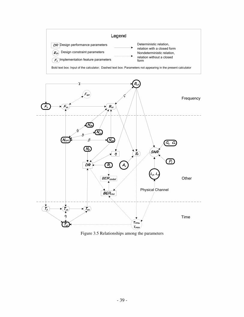
The interrelationships between the key parameters are either deterministic or non-

deterministic. For the former, it is always possible to find an analytic equation between

the relevant parameters; for the latter, we can either utilize estimates of the parameters

involved wherever possible, or define a fourth category of parameters, so-called relation

parameters, to help describe the relationships.

Based on the above idea, the OFDM Calculator has been implemented, which takes a

subset of the parameters as basic inputs and automatically generates other parameters.

The core of the OFDM Calculator is the calculation of design performance parameters, i.e.

data-rate, spectral efficiency and BER estimate, while the design constraints and

- 31 -

implementation features will directly or indirectly contribute to the calculation. In

addition, a link budget calculation and other additional features have also been

implemented.

3.2.1 Data rate and spectral efficiency calculation

Assume all the subcarriers used adopt the same modulation scheme, i.e. without bit-

loading10

, it is easy to find that the un-coded data-rate DRraw is directly related to the un-

extended symbol length Tus, the guard interval length Tgi, the number of data subcarriers

Nds, and the number of bits per subcarrier per symbol Nb (the parameter representing the

modulation scheme), as follows:

=+

ds b

raw

us gi

N NDR

T T. (3.1)

Notice Tus is also the length of one FFT window, so for a system with FFT size NFFT,

sampling period Ts and sampling frequency Fs, Tus is:

= =FFT

us FFT S

s

NT N T

F. (3.2)

Thus (3.1) could be rewritten as:

11

= = × ++

ds b ds s b

raw

giFFT gi FFT

uss us

N N N F NDR

TN T N

TF T

. (3.3)

In order to reflect the impact of parameter choice on the system performance, we can

define a series of relation parameters, namely the guard interval (GI) to un-extended

symbol length ratio α, the data subcarrier number to FFT size ratio β, and the sampling

factor [MAN04] γ, to be:

=gi

us

T

Tα , (3.4)

10Equation (3.1) could be easily modified to take bit-loading into consideration. However, since the

proposed system, as a wireless transport system, will not adopt bit-loading, the OFDM Calculator has not

implemented this feature.

- 32 -

=ds

FFT

N

Nβ , (3.5)

=s

ch

F

Bγ , (3.6)

respectively, where Bch is the channel bandwidth, then the un-coded data rate could be

written as:

1=

+

ch b

raw

B NDR

βγ

α. (3.7)

Assume the channel coding rate is Rc, then the coded data rate DR and the spectral

efficiency of the system η, are:

1=

+

ch b cB N RDR

βγ

α, (3.8)

1=

+

b cN Rβγη

α. (3.9)

Now we can discuss the effect on the data rate and the spectral efficiency, and other

important aspects of the system, when adjusting relevant parameters.

First we need to check the significance of α . It indicates the transmission capacity

loss due to the time domain processing. This loss could also be expressed as SNR loss.

Since no information is transmitted during the GI period, the SNR loss due to the

insertion of the GI, SNRloss, could be calculated as [Eng02]:

10 10

110log 10log

1

= − = −+ +

usloss

us gi

TSNR

T T α. (3.10)

Based on (3.8) and (3.9), it is obvious we should reduce α , i.e. increase Tus and/or

reduce Tgi to get a higher data rate and spectral efficiency. However, their values are not

obvious to determine. For Tgi, enough length should be given for combating the ISI.

[NP00] suggests it be two to four times of rmsτ , the root-mean-squared delay spread11

,

while [Eng02] suggests that it should be as long as the length of the channel impulse

11 More on rmsτ will be discussed in section 3.3.

- 33 -

response, and furthermore, the filter response (of all the filters cascaded inside the system)

also needs to be incorporated into the channel impulse response.

As for Tus, there are two major constraints regarding its length. One constraint is the

channel coherence time: If the OFDM symbol is too long then the channel could not be

taken as time-invariant between consecutive channel estimation intervals and so the

performance will be degraded. The second, a more important constraint, is the

relationship between carrier recovery error Ferr and subcarrier spacing Fss, the inverse of

Tus. A detailed analysis of the effects of carrier recovery error is beyond the scope of this

thesis12

. An empirical requirement provided by [FK03] is:

0.02= <err

err us

ss

FF T

F. (3.11)

So Tus should take an appropriate value to alleviate the difficulty of carrier recovery.

Next we will check the significance of β andγ . β could be interpreted as the FFT

efficiency, representing how much of the FFT computation capability is contributing to

information transmission13

, while γ could be interpreted as the cost associated with

flexible up-sampling frequency choice, which can relax the reconstruction and anti-

aliasing filter sharpness requirement.

Based on (3.8) and (3.9), it seems that both β and γ should be increased to achieve

higher data rate and spectral efficiency. However, these two parameters are restricted by

the filtering requirement, as explained in the next section.

3.2.2 Filter sharpness requirement

As seen in Figure 3.3(a), the frequency band corresponding to Fs is divided into NFFT

equal-sized slots. In addition to Nds as the data subcarriers number, assume the number of

subcarriers used for pilot and signalling is Nps, for DC-Offset and notch is Ndn, then the

bandwidth corresponding to (Nds + Nps + Ndn) subcarriers is defined as the major energy

12 Simply put, carrier recovery error will introduce ICI and its effect could be modeled as AWGN if the

number of subcarriers is considerable. 13 This interpretation holds even when the FFT is used to directly manipulate only real signals, where β is

always less than 1/2 since in the frequency domain, half of the points are only the complex conjugate of the

other half. But the loss of FFT calculation capability has the payback of requiring only a single ADC and a

single DAC.

- 34 -

bandwidth (Bsc). The amplitude response mask specification for the low-pass

reconstruction and anti-aliasing filter14

is shown in Figure 3.3(b), where the passband and

stopband corner frequencies are ωp and ωs respectively, while the amplitudes for

passband and stopband are assumed to be 0 dB and As dB respectively.

(a)

(b)

Figure 3.3 Filter sharpness requirement. (a) Relationship between Bsc, Bch and Fs; (b) Filter

amplitude response requirement

14 In over-sampled system, the digital low-pass anti-aliasing filters are also included

- 35 -

The sharpness of the filter is a very critical parameter since it determines the degree

and thus the cost of the filter. It can be represented by the slope of the line in the

transition band, Sf, in dB/decade, calculated as:

1010loglog

= =

s s

f

scs

chp

A AS

B

B

ω

ω

. (3.12)

Since for a particular system, As is determined by the allowed radiated power into

neighbouring bands and the ADC resolution, it is normally a fixed known value. We

could thus define a filter sharpness factor, ς, to describe the filter sharpness requirement,

as following:

( ) ( )+ + + += = =

ds ps dn ss ds ps dnsc

FFT SSch FFT

N N N F N N NB

N FB N

γς

γ

. (3.13)

If we define the pilot and signaling subcarrier number to FFT size ratio δ, the DC-

Offset and notch subcarrier number to FFT size ratio θ, to be:

=ps

FFT

N

Nδ , (3.14)

=dn

FFT

N

Nθ , (3.15)

then (3.13) could be rewritten as:

( )= + +ς β δ θ γ . (3.16)

δ and θ could be interpreted as the FFT computation capability loss due to the overhead

of pilot and signaling, DC-Offset and notch, respectively. Meanwhile, since ς must be

less than 1, β and γ cannot be arbitrarily raised to achieve higher data rate and spectral

efficiency, as mentioned in last section.

While ( )+ +β δ θ γ represents the filter sharpness requirement, ( )1− + +β δ θ γ

could be interpreted as the capacity loss due to filtering. It is desirable to decrease this

loss, but a sharper filter will add additional dispersion to the channel impulse response,

- 36 -

and the GI length may need to be increased to combat the additional loss. It is possible to

find theoretical optimal values of the GI length and the filter specification such that the

overall capacity loss is minimized [Fau00], but considering the dynamic nature of the

channel, and the implementation cost, empirical choices are made instead.

So far the impact of the modulation scheme and channel coding, i.e. Nb and Rc, have

not been mentioned. They are heavily determined by achievable Signal-to-Noise-Ratio

(SNR), desired BER, and implementation cost, as discussed later.

3.2.3 BER estimate

In an Additive White Gaussian Noise (AWGN) channel, the BER performance of an

OFDM system should be the same as that of a single carrier system, except that the

equivalent SNR should take the power loss due to the guard interval into consideration.

Take a system with BPSK or QPSK for example, the BER is given as [HP03]:

( ),

1

2= =b AWGN bBER P erfc SNR , (3.17)

where erfc(x) is the complementary error function given by

22( )

∞−= ∫

t

x

erfc x e dtπ

, (3.18)

and SNRb is the effective SNR per bit that has taken the SNRloss as given by (3.10) into

account.

For an M-ary square QAM modulation scheme (e.g. 16-QAM used in the proposed

system), there is no a simple closed form equation to calculate the BER. The probability

of symbol error could be approximated by [Hay01]:

( ),

1 32 1

2 1

− −

b

s AWGN

SNRP erfc

MM� , (3.19)

and for the M-ary square QAM using Gray code (as will be implemented in the proposed

system), it can be shown that [Hay01]:

,

,

2log

≤ ≤s AWGN

s AWGN

PBER P

M. (3.20)

- 37 -

So these two bounds can be used to estimate BER.

In a more realistic channel, e.g. a Rayleigh fading channel, [HP03] has provided a

thorough theoretical analysis. We propose a more general approach assuming the channel

is known. Based on the channel knowledge, the equivalent SNR per bit of each subcarrier

could be calculated as

, ( )=b i bSNR SNR H i (3.21)

where H(i) is the term of the transfer function corresponding to subcarrier i. The BER for

each subcarrier could be calculated based on SNRb,i, and the BER of the system could be

calculated as the average of the BER for each subcarrier. However, this is only a loose

lower bound of the real system since the channel impulse response is supposed to be

known, and other noise in the system, e.g. the noise introduced by synchronization error,

and the noise smearing caused by the FFT windowing in the receiver side [Bin00], has

not been taken into account.

3.2.4 Link Budget calculation

A link budget is used to determine if the power and noise related operating conditions,

such as transmitted power level, transmitter antenna gain and receiver antenna gain could

guarantee the required SNR, and if so, how much design margin is left.

Tx Antenna Gain

Rx Antenna Gain

Path Loss Other Loss Noise FigureTx Power

Antenna Thermal Noise Power

Rx Power +

Figure 3.4 Link budget model

As shown in Figure 3.4, the received signal power Pr (expressed in dBm) is:

= + − − +r t t p o rP P G L L G , (3.22)

where

Pt is the transmitted power in dBm;

Gt is the transmitter antenna gain in dB;

Lp is the path loss in dB;

- 38 -

Lo is other loss in dB, caused by the channel, such as shadow, reflection, etc;

Gr is the receiver antenna gain in dB.

The path loss Lp could be calculated as [LMC04]:

10

420log

=

cp

dFL

c

π, (3.23)

where d is the distance between the transmitter and the receiver, Fc is the carrier

frequency, and c is the speed of light (3x10⁸ m/s).

The noise in the system could be modeled as two parts, the thermal noise picked up

by the antenna, represented by Pn, and the noise added by the receiver analog front-end,

represented by the noise figure NF. Pn could be calculated in dBm as[LMC04]:

( )1010log 30= +n chP kTB , (3.24)

where k is Boltzmann’s constant (1.38x10⁻²³

J/K), T is the Kelvin temperature of the

antenna, and Bch is the channel bandwidth.

So the achievable SNR is

= − −r nSNR P P NF , (3.25)

and if the required SNR is SNRreq, then the design margin is

= −m reqSNR SNR SNR . (3.26)

The above model only provides a first-order estimate, since the physical channel has

been simplified, and other sources of the noise, e.g. the transmitter noise, transmitter non-

linearity [LMC04] and the interferences from neighboring channels, have been ignored.

However, the result could still provide insight into the achievable SNR.

So far the interrelationships among the parameters have been briefly discussed. Figure

3.5 diagrammatically summarizes the relationships. Based on the rapid exploration results

generated by the OFDM Calculator, a detailed Matlab model for the proposed 60 GHz

radio was built, which will be introduced in the next section.

- 39 -

Physical Channel

Frequency

Other

Time

Design performance parameters

Design constraint parameters

Implementation feature parameters

Deterministic relation,

relation with a closed form

Nondeterministic relation,

relation without a closed form

3

Bold text box: Input of the calculator; Dashed text box: Parameters not appearing in the present calculator

Figure 3.5 Relationships among the parameters

- 40 -

3.3 Proposed 60 GHz System

This section will demonstrate the system-level design results of the proposed OFDM-

based 60 GHz radio. First the adopted channel model will be introduced, and then the

design results will be elaborated.

3.3.1 Channel model

A channel model plays a vital role in digital communication systems, and it is especially

true for OFDM systems where the overhead, efficiency and BER performance are

directly or indirectly related to the characteristics of the channel, as depicted in Figure 3.5.

60 GHz in-door channel models have been widely studied in the research community

[DT99][MC02][PKH98][BRO03]. A complete channel model covers three mechanisms

existing in the physical channels, namely path loss, shadowing and multi-path

interference, via large-scale and small-scale channel models, revealing both static and

dynamic features of the channels [PRA04]. Considering the impact on OFDM system

design, the introduction of a channel model in this section will focus on the most

important aspects of the multi-path interference, and related results for 60 GHz in-door

channels.

A multi-path channel consists of multiple paths each of which could be characterized

by its amplitude, phase and the propagation delay. The time-variant impulse response of

the channel, as a contribution of all the paths, can be denoted as h(t, τ), representing the

impulse response of the channel at time t due to an impulse applied at time t- τ [FK03].

The complex baseband equivalence of h(t, τ) is [BRO03] [Pra04]:

( ) ( )1

0

,−

=

= −∑k

k

Nj

k k

k

h t a eθτ δ τ τ , (3.27)

where Nk is the variable number of paths, ak, θk and τk are the amplitude, phase and

propagation delay of the kth path respectively, and δ( ) is the Dirac delta function. Based

on the impulse response, the channel transfer function is

( ) ( )1

2

0

,−

=

= ∑k

k k

Nj f

k

k

H f t a eθ π τ

. (3.28)

- 41 -

Generally ak, θk and τk are time variant and many studies have been carried out on the

modeling and measurement of their statistics. We are especially interested in the

propagation delay of the channel due to its impact on the OFDM systems. The maximum

delay τmax and the root mean square delay spread τrms could be defined to summarize the

propagation delay feature. Assume that the shortest path has a propagation delay of zero,

then τmax is the longest delay among all the paths, while τrms is

12 2

0

12

0

( )−

=−

=

=∑

k

k

N

k m k

krms

N

k

k

a

a

τ τ

τ , (3.29)

where τm is the mean delay spread defined as

12

0

12

0

=

=

=∑

k

k

N

k k

km

N

k

k

a

a

τ

τ . (3.30)

The channel impulse response of an in-door channel, and hence τmax and τrms are

determined by the room geometry and material, relative locations of the transmitter and

receiver, antenna radiation patterns, and whether it is LOS or NLOS situation. Due to the

above factors, different research results have been reported. For example, [MC02]

presents a multi-ray-tracing model for a long corridor of 44x2.20x2.75 m3, with brick and

plasterboard surface wall and LOS situation. The simulated τrms varies with transmitter

and receiver distance from 0.57 ns to 2.32 ns using isotropic antennas. When the value of

τrms using isotropic antennas is 2.13 ns for a transmitter and receiver distance of 30 m, it

changes to 1.18 ns and 1.58 ns with Omni-Omni and Horn-Horn antennas respectively.

[PKH98] gives both measurements and a statistical model results for a typical office with

windows, partitions and furniture. Different relative position and antenna configurations

were carried out and the τrms is less than 55 ns for all possibilities. [DT99] used a ray-

tracing based model for an office with furniture. The cumulative distribution function of

the τrms shows that τrms is up to 20 ns, while the probability of τrms > 10 ns is 6% to 20%

depending on the receiver antenna types.

- 42 -

In our research, both AWGN and time-invariant multi-path channel are used to

simplify the simulation. The multi-path channel model is generated by assuming a

number of propagation paths with random lengths, and restricting τrms <55 ns.

3.3.2 Design results

With the objective of supporting the Gigabit Wireless Ethernet (GWE), the most crucial

parameters for the proposed 60 GHz system are summarized in Table 3.1, and a detailed

comparison with other OFDM standards is given in Appendix A, where another

comparison of our proposed design with other two 60 GHz OFDM projects is also given.

Parameter Symbol Value

Channel bandwidth Bch 512 MHz

Sampling frequency Fs 512 MHz

Sampling factor γ 1

FFT size NFFT 1024

Number of used subcarriers Nsc 912

Number of data subcarriers Nds 880

Nds to NFFT ratio β 0.86

Number of pilot and signaling subcarriers Nps 32

Nps to NFFT ratio δ 0.03125

Number of DC & notch subcarriers Ndn 1

Ndn to NFFT ratio θ 1/1024

Sample period Ts 1/512 µs

Un-extended symbol length Tus 2 µs

GI length Tgi 0.25 µs

Tgi to Tus ratio α 1/8

Extended symbol length Tes 2.25 µs

Sub carrier spacing Fss 500 kHz

Major energy bandwidth Bsc 456.5 MHz

Filter sharpness factor ς 0.89

Modulation BPSK, QPSK, 16-QAM

FEC coding TBD

Max. uncoded data rate DRraw 1.56 Gbps

Max. data rate DR TBD

Max. spectral efficiency (uncoded) ηraw 3 b/s/Hz

Table 3.1 Proposed 60 GHz OFDM System

Some important considerations when choosing these parameters are:

- 43 -

o The maximum DRraw reaches 1.56 Gbps, so with reasonable channel coding,

supporting GWE is possible. However, the choice of channel coding technique

needs further research.

o The maximum spectral efficiency for the uncoded system is 3 b/s/Hz.

o The BER performance target is application dependant. For instance, MPEG-2

video requires BER=10-11

, and in DVB-T this is achieved using a concatenated

convolutional code and Reed-Solomon code, while the BER performance after the

Viterbi decoding for the convolutional code (i.e. the inner code performance) is

required to be 2×10⁻⁴

[DVB04]. For the proposed baseband system without coding,

a BER performance target of 10-4

is considered. To meet this BER performance

target, the RF front-end proposed by [Yao05] is assumed, which can provide

transmitter power (Pt) of 20 dBm15

and transmitter antenna gain (Gt) of 20 dB.

When the distance is 10 m, the SNR is 19.55 dB with 20 dB design margin.

o Fs is chosen to be 512 MHz so that the DAC and ADC with the required ENOB

(Effective Number Of Bits) of 10 bits16

are technically feasible.

o NFFT is 1024 so that a radix-4 FFT/IFFT could be adopted.

o The choice of Tgi as 250 ns is based on the observation that τrms is less than 55 ns

in [PKH98] and the rule of thumb that GI should be two to four times of τrms as

proposed in [NP00].

o The impact of FSS17

needs further research.

o Nps and Ndn need further research.

The proposed modulation and demodulation core will incorporate all the functions as

shown in Figure 2.8. Some of the involved design aspects cannot be described by Table

3.1, e.g. the exact form of the time domain window, and the frequency domain processing.

These features are embedded into the Matlab model and simulated to evaluate the design

choice. The BER performance simulation results for the system-level model, a double-

15 This is within the 40 dBm EIRP (Effective Isotropic Radiated Power) emission regulation of the 60 GHz

band [Yao05][FCC05]. 16 See the finite word-length effect evaluation section of Chapter 4. 17 The Broadway project, targeting in next-generation wireless LAN operating at 60 GHz, chooses FSS to be

512 kHz [BRO04].

- 44 -

precision-floating-point number based model, can be found in Appendix C, where it is

compared with architectural level model simulation result.

- 45 -

4. Architectural Level Design

This chapter describes the architectural level design for the proposed OFDM system. First,

the design challenges and proposed solution are introduced, and then the overall design is

summarized. Next the detailed fixed-point model transformation and hardware

transformation of the FFT/IFFT block are elaborated.

4.1 Design Challenges and Proposed Solution

Architectural level design is the design phase that transfers a system level model into a

hardware oriented model, exploring the intrinsic parallelism of the algorithm, studying

implementation alternatives and making architectural decisions.

The most dominant design challenge at the architectural level of the design is to

achieve the desired performance with minimum cost. Architectural level design has

considerable impact on the intrinsic hardware performance and cost criteria such as

timing, area and power. For the modulation and demodulation cores, the timing

requirements are especially challenging. Furthermore, functional performance criteria are

also affected by architectural level design choices, – when the algorithmic model is

transformed into an architectural model, the ideal assumptions made in the algorithmic

model are usually simplified or replaced by the non-ideal hardware to lower the

implementation cost with acceptable performance loss. For example, finite word-length

effects impose additional noise onto the system, and the BER performance will be

degraded.

An iterative design flow is adopted, as shown in Figure 4.1. Major architectural level

design tasks of the proposed system include:

Fixed-point model transformation. Unlike the unlimited-precision algorithmic

model used in the system level design, the architectural model is based on fixed-point

number18

with finite word-length. To alleviate the degradation caused by possible

truncation, rounding or overflow due to the finite word-length, sufficient word-length,

18 An algorithm can also be implemented in floating-point format, but with higher area and power cost.

Besides, the floating-point implementation is not necessary for the proposed system.

- 46 -

appropriate position of the decimal points, and proper scaling should be assigned to all

the data operands. On the other hand, wider word-lengths will result in larger area, slower

data-path and larger power consumption. A systematic method must be adopted for

optimizing the finite word-lengths in the system to balance the performance loss and the

area and timing penalty.

Word-length optimization

Functional Performance Acceptable?

Y

Performance and cost Acceptable?

Y

Next design phase(RTL design and backend flow)

N

N

Fixed-point model transformation

Hardware transformation

Allocation

Scheduling

Binding

Figure 4.1 Architectural level design flow

Hardware transformation. An ideal solution for the hardware transformation

problem is to have a high-level synthesizer to automatically synthesize the algorithmic

model into RTL (register transfer level) model. Some commercial tools, e.g. [ACC05],

are presently available. Due to the high throughput requirements and the complexity of

the design considered in this thesis, a manual transformation process is adopted.

- 47 -

Nevertheless, like the high-level synthesis EDA tools [GR94], the following three tasks

also exist in the manual procedure:

Allocation: Determining the number and functionality of the processing elements (PEs);

Scheduling: Deciding the start time of individual operation;

Binding: Assigning the operations to available PEs.

These steps could occur repeatedly at different granularity until the RTL code could be

easily generated from the specification. For instance, generally two granularity levels, the

macro architectural design and the micro architectural design will happen, where the

former focuses on functional block identification, block interface definition, global

control and data flow arrangement, while the latter focuses on pipelining and parallel

processing unit arrangement, detailed data-path and local control design.

As seen in Figure 4.1, the fixed-point model transformation and the hardware

transformation may happen iteratively, because the word-lengths of the fixed-point model

will affect the architecture choices. For instance, operations involving the same function

and same word-length could easily share one PE, while it may be better to allocate

different PEs for the operations with different word-lengths even if the operations are

identical.

For the baseband processing system, the fixed-point model transformation will be

carried out using statistical analysis and simulation, while a graph projection technique

[Kun88] will be utilized to tackle the three tasks involved in the hardware transformation

simultaneously.

4.2 Overview of the Design

The block diagram of the macro architecture is shown in Figure 4.2. It is different from

the functional block diagram of Figure 2.8 since the blocks in Figure 4.2 correspond to

the physical building units instead of abstract functionality.

The system works in one of two modes: transmitter mode, where all the blocks with a

dark background are involved, or receiver mode, where all the blocks with a light

background are involved. The functions of the individual blocks are:

- 48 -

Input Buffer Modulator Framer

Output Buffer Demodulator Deframer

FFT/ IFFT

I, Q I, Q

I, QI, Q

Data in

Data out

DAC data

(I, Q)

ADC data

(I, Q)

Figure 4.2 Architectural block diagram of the proposed system

Input Buffer / Output Buffer: Isolate the modulation and demodulation core from the

rest of the system, so that flow control could be simplified and the system can work in

a “best effect” manner with simplified global control.

Modulator: Implements the constellation mapping and frequency domain processing

functions with a loop-up table based method as discussed later.

Demodulator: Implements the frequency domain correction and constellation

demapping functions.

FFT/IFFT: Acts as IFFT block in transmitter mode and FFT block in receiver mode.

Framer: Implements the time domain processing functions.

Deframer: Implements the frame synchronization functions.

In the transmitter mode, once the input buffer is filled above a configurable threshold

depth, the transmitter path will begin working to periodically generate the OFDM mega-

symbols, until the buffer is empty. Zero values may need to be padded into the data

stream read from the buffer to generate a complete mega-symbol.

In the receiver mode, a start-of-symbol signal initiates the receiving processing

procedure, and the demodulated data stream is stored in the output buffer, waiting to be

read out.

At the macro architectural level, a macro pipeline is formed by all the blocks with the

workload unit of a mega-symbol. That is, each mega-symbol will encounter an identical

processing flow in any block, while different blocks could work on different mega-

symbols simultaneously. Meanwhile, each block contains its own micro pipeline with the

- 49 -

workload unit of a data sample, so a block could work on multiple samples that belong to

either one mega-symbol or adjacent mega-symbols simultaneously. This two layered

pipelining provides a processing stream that has short latency and high PE efficiency.

To provide enough throughput, in addition to the pipelining, four parallel processing

datapaths are also used, as explained later.

Of all the blocks shown in Figure 4.2, the FFT/IFFT block is the most critical and

challenging block, since it is the performance bottleneck and its finite word-length effects

determines the overall fixed-point model of the system. Other blocks in Figure 4.2 can be

(relatively) easily implemented based on their functional description. So in the following

sections, the FFT/IFFT block will be further described.

4.3 FFT/IFFT Block

For the 1024-point FFT/IFFT used in the proposed system, both radix-2 and radix-4

algorithms are possible architectural alternatives, but a radix-4 architecture is used since

it is possible to implement 4 parallel data-paths to meet the throughput requirement

without introducing a critical timing closure problem. To illustrate the algorithm, the SFG

(Signal Flow Graph) of a radix-4 DIF (Decimation In Frequency) 64-point FFT is shown

in Figure 4.3, where the base of the twiddle factors, ( )/8−=

jW e

π. A basic building block,

the radix-4 butterfly is shown in Figure 4.4, which consists of four 4-input complex

number adders (also named the crossadder due to the geometric shape) and 3 complex

number multipliers (also named the rotator since the complex number multipliers only

rotate the phases of the input complex number without changing their amplitudes).

The following sections will discuss the fixed-point model transformation and the

hardware transformation of the IFFT/FFT block in detail.

- 50 -

X[0]

X[4]

X[8]

X[12]

X[1]

X[5]

X[9]

X[13]

X[2]

X[6]

X[10]

X[14]

X[3]

X[7]

X[11]

X[15]

W0

W0

W0

W0

W0

W1

W2

W3

W0

W2

W4

W6

W0

W3

W6

W9

W0

W0

W0

W0

W0

W0

W0

W0

W0

W0

W0

W0

W0

W0

W0

W0

x[0]

x[1]

x[2]

x[3]

x[4]

x[5]

x[6]

x[7]

x[8]

x[9]

x[11]

x[12]

x[13]

x[14]

x[15]

x[10]

Figure 4.3 16-point radix-4 DIF FFT SFG

Figure 4.4 Butterfly of radix-4 DIF FFT

- 51 -

4.3.1 Fixed-point model transformation of the FFT/IFFT block

4.3.1.1 Issues for fixed-point model transformation

When transferring the FFT/IFFT block into a fixed-point model, sources of noise include

the round-off noise in rounding the results of the complex multipliers to retain certain

word-lengths, the round-off noise in scaling the data to prevent overflows, and the

quantization noise in representing the twiddle factors using finite-word-length. These

effects happen in each stage of the algorithm and are propagated along the calculation

path. In addition, other factors such as number representation scheme also affect the

characteristics of the noise. Specifically, in the context of OFDM systems, one needs to

determine the following issues for the fixed-point model transformation:

Number representation scheme. The number representation choice will affect the

type of computational elements and implementation costs. A two’s complement number

system is chosen since it generally gives good results and it is well supported by the

dedicated multipliers of the targeted prototype FPGA19

.

Single word-length vs. multiple word-length. In a single word-length scheme, a

uniform word-length is used to represent all data operands, while in a multiple word-

length scheme, the word-lengths for individual data operands could be freely chosen

when necessary [CCL01] [CCL04]. We will focus on the multiple word-length scheme

since it can provide a good balance between performance and cost.

Word-lengths of individual objects. For each FFT stage, the word-lengths for the

crossadder input and output, the twiddle factors, the intermediate results and the final

results all need to be determined. This will be a major task and it will be further discussed

later.

Static scaling vs. dynamic scaling. In a static scaling scheme, the scaling factor of

each FFT stage is fixed, so the implementation is simple but the range of represented data

is also fixed. A dynamic scaling scheme, such as the convergent Block Floating Point

(BFP) [BCJ95] scheme, will decide the scaling factor according to the calculation result

on-the-fly, and it could combine the benefits of both the floating-point and the fixed-point

19 For an ASIC version, DesignWare from Synopsys also supports two’s compliment arithmetic well.

- 52 -

paradigms. The static scaling scheme will be chosen since consecutive OFDM samples

are transmitted in the same signal amplitude level and thus require the same word-length

format, so it is not necessary to consider the dynamic scheme, at least in the transmitter

side. In addition, as shown later, the static scheme could meet the performance

requirements with reasonable cost.

Degradation schemes. Whenever an overflow is about to happen20

, a choice must be

made to let it overflow freely or saturate instead. Meanwhile, choice must be made

between rounding and truncation to constrain word-length increase.

Numerical value mapping. The modulated complex symbols from the modulator as

shown in Figure 4.2, e.g. 1

( 3 3j)10

± ± for a modulation scheme of 16-QAM, need to be

further mapped into appropriate values to make the best use of the calculation capability

of the architecture, so that the highest possible SNR could be achieved. At the same time,

the DAC/ADC has certain ENOB limits, so the sample values after the IFFT need to be

mapped into the DAC appropriately so that the achieved PAPR and the SNR degradation

are within specification.

In the following sections, based on previous research on the finite word-length effects

of the FFT, a proposed solution particularly targeted at the overall fixed-point model

transformation for the OFDM system will be described.

4.3.1.2 Summary of previous research on the finite word-length effects of FFT

Appendix B gives a detailed description of two previous studies on the effect of finite

word-length on FFTs. Some useful observations are:

1). Overflow is regarded as a severe degradation, and so it is to be avoided by all

means. Scaling is a widely used approach to prevent overflow. One scaling method is to

only scale the input of the FFT, and it has been shown in [OSB99] that such a scaling

method in the single word-length FFT implementation has the signal-to-noise ratio of

2

2

2=

B

fweSNRN

, (4.1)

20 Overflow can be totally avoided in the FFT algorithm itself by appropriate scaling. However, as will be

seen later, when the time-domain sample values are mapped to DAC input, overflow events are still of

concern.

- 53 -

for an N-point radix-2 DIT (Decimation In Time) FFT with word-length of (B+1)-bits.

An improved scaling method to prevent overflow is to scale the input of each FFT stage.

It has been shown in [OSB99] that once the input to the FFT could guarantee no overflow

in the first stage21

, then for a radix-2 FFT simply scaling the input of each FFT stage by

½ can prevent overflow in all stages and the signal-to-noise ratio is now

22

4=

B

fweSNRN

. (4.2)

2). Since scaling will generate additional noise, a better method to prevent overflow is

to increase the word-length of each FFT stage. Once the input to the FFT could guarantee

no overflow in the first stage22

, then for a radix-2 FFT simply increase the word-length of

each FFT stage by one bit can prevent overflow. This is actually the root of multiple

word-length scheme used in FFT.

3). A combination of scaling and word-length expanding lets the word-length increase

for the early stages, and maintain a fixed word-length but use scaling after a certain stage

to achieve a balance of performance and area cost, because the noise source in the early

stages have more negative effect and so it is better to avoid scaling in the early stages.

[PD01] presents a detailed noise model for analyzing this kind of combined

implementation.

The above finite word-length effects analysis can provide a good insight and guideline

for the appropriate word-length choice. It is also worth noting that the above method can

be adapted for any radix algorithm, once the word-length scheme is static and uniform

per stage. Take radix-4 FFT/IFFT for example, to prevent overflow, the required scaling

is 1/4 or the required word-length expansion is 2 bits.

However, to fully resolve all the issues for the fixed-point model transformation, the

cascade of individual blocks in the signal processing chain needs further analysis. Besides,

21 If all numbers are interpreted as fractional number, then a scaled sequence whose real and imaginary

parts are uniformly distributed between 1/ 2− and1/ 2 is a sufficient sequence to guarantee no overflow

in the first FFT stage. However, since this input also needs to be scaled by 1/2 before the first stage, we can

supply a sequence whose real and imaginary parts are uniformly distributed between 1/ 2 2− and1/ 2 2 ,

and only scale the inputs of other stages except the first stage.

22Again a scaled sequence whose real and imaginary parts are uniformly distributed between 1/ 2−

and1/ 2 is a sufficient sequence to guarantee no overflow in the first FFT stage.

- 54 -

no clue has been given for the numerical value mapping issue. The following section will

present an overall solution.

4.3.1.3 Proposed solution

The general idea of the proposed solution is: First, assume the IFFT, FFT are ideal

without finite word-length effects, and the quantization only happens at the DAC/ADC,

then find the appropriate ENOB for the DAC/ADC and the numerical value mapping

scheme to meet the PAPR requirement and BER requirement; Second, analyze and

choose the appropriate FFT/IFFT word-length scheme so that the achieved performance

of the previous step will not be seriously degraded; Finally, verify and fine-tune the

choice with simulation. Detailed description of this solution follows.

Assume the IFFT and FFT are ideal, then the statistics of the time-domain OFDM

signal need to be studied to evaluate the quantization effect of the DAC and ADC. As

explained in Chapter 2, both the in-phase and quadrature components of the OFDM

signal are very close to a Gaussian process with zero mean and variance σ2 , and two

DACs and two ADCs are needed in the transmitter side and the receiver side respectively.

To quantize these two signals, two questions need to be answered:

What range of the signal needs to be quantized? As seen in Figure 4.5, if [-uσ, uσ] is

the range of the signal to be quantized, then what is an appropriate value for u?

How many bits are needed to quantize this data range? i.e. what should the ENOB be ?

The quantization procedure could be modeled as an ideal quantization with infinite

precision followed by two kinds of additive quantization noise, the clipping noise and the

rounding noise, as shown in Figure 4.5. A clipping noise is introduced once clipping

happens and the variance of the noise is inversely proportional to the value of u, while the

rounding noise happens for every data sample and is determined by both u and the ENOB:

if u is unchanged, then larger ENOB will result in smaller rounding error variance; if

ENOB is unchanged, then larger u will result in bigger rounding error variance.

- 55 -

+Quantized signal

Rounding noise

Clipped value

2 steps

Clipping noise

Infinite

-

Figure 4.5 DAC/ADC quantization model with clipping noise and rounding noise

So the clipping noise and rounding noise present conflicting requirements in the

selection of u. At the same time, considering the allowed PAPR of the system, especially

the achievable linearity range of the analog front-end, it is desirable to have a smaller u.

An empirical value of u provided by [HP03] is around 3 or 4, since under such values the

clipping probabilities are about 3x10⁻³

and 6x10⁻⁵

respectively, and are negligible

compared with other noise sources in the system. However, the corresponding PAPRs are

about 9.5 dB and 12 dB respectively, probably still too high for the analog front-end. So

the final choice may depend on the overall allowed PAPR of the analog front-end.

For the rounding noise, assume BQ bits are used for both the DAC and the ADC23

.

Since the in-phase and quadrature are both Gaussian distributed, it can be proved that the

rounding noise is zero-mean and its variance is [SS77]:

( )2

2 2 2 2

2 2 21

112 21 exp

12

=

− ∆= + −

∆ ∑

n

Q

n

n

n

π σσ

π, (4.3)

where ∆ is the quantization step defined as

2

2∆ =

QB

uσ. (4.4)

It can also be shown that when / 1σ ∆ ≥ , (4.3) is very close to 2 /12∆ and so the error

follows a uniform distribution. This condition is easily satisfied since

23 The ENOB for ADC should not be less than that of DAC, so that the performance achieved at the

transmitter could not be lost by the ADC, at the same time certain margin is left for the AGC (Automatic

Gain Control) misalignment. For brevity, here the ENOBs for ADC and DAC are assumed to be the same.

- 56 -

12 −

=∆

QB

u

σ. (4.5)

We are very interested in the signal-to-noise ratio, which is

22

2 2 2

2

3 2

12

⋅= =

QB

Q u

σ σ

σ, (4.6)

or in dB form:

2

2 2

10 10 10 102

3 210log 10log 3 20 log 2 20log

⋅= = + −

QB

Q

Q

B uu

σ

σ. (4.7)

So one more bit of BQ will give 6 dB more signal-to-noise ratio. Table 4.1 illustrates a

series of possible design choices for the proposed baseband processing system. The

signal-to-noise ratio should be interpreted with caution: First, the clipping noise of the

quantization procedure has been ignored under particular choice of u; Second, the

rounding error is uniformly distributed, so its effect on the final BER performance is not

Gaussian. Nevertheless, it still gives a good insight into possible system performance, and

its usage will be justified by simulation.

u BQ SNRid_fft

3 8 43.4 dB

3 10 55.4 dB

3 12 67.4 dB

4 8 40.9 dB

4 10 52.9 dB

4 12 64.9 dB

Table 4.1 Signal-to-rounding-noise ratio with ideal IFFT/FFT

Now the finite word-length effects of the IFFT and FFT and the numerical value

mapping scheme should be considered. Figure 4.6(a) illustrates all the blocks that are

closely related to the finite word-length effects of the IFFT and FFT, and the word-

lengths between adjacent block boundaries. Only the in-phase component of the complex

baseband signal is demonstrated for brevity since the quadrature component will traverse

a similar datapath.

- 57 -

Data in Constellation Mapping

Scalingup by

IFFTClipping

& Rounding

DAC

Modulator

+

Channel

FFT ADC AGC

+

Same block configured in different modes

(a) Overall finite word-length effects relationship

+ ++

+ ++

+

(b) Simplified noise model

Figure 4.6 Proposed noise analysis model

At the transmitter side, the constellation mapping function maps the input data stream

into a random sequence IM, corresponding to the power-normalized in-phase component,

with the variance of 1/2. For example, in the case of 16-QAM, IM consists of symbols

from { }1/ 10, 3 / 10± ± . IM will be mapped to IS by multiplying a mapping factor p,

which is not necessarily a power of 2. After this scale-up, IS could be represented as a BQ-

bit integer with variance p2/2. The word-length of the input number into the IFFT is BQ, a

number generated from last design step, because the IFFT/FFT is a shared block, and the

ADC feeds BQ-bit number into the FFT. Following the observation of [PD01], the

IFFT/FFT will increase the word-lengths till BQ + E in the early IFFT/FFT stages, and

keep the word-lengths as BQ + E for the rest stages. So the IFFT is not following the

standard definition as in equation (2.2), rather it is

� �21

0

2[ ] [ ]

=

= ∑j nkE N

NI s

k

I n I k eN

π

n = 0, 1, …, N-1, (4.8)

- 58 -

where�[ ]II n and �[ ]sI k are the complex signals corresponding to [ ]II n and [ ]sI k respectively.

The clipping and rounding block rounds the least L bits and clips the highest E-L bits. If

the clipping and rounding error is ignored, then

2= I

CRL

II , (4.9)

It is zero-mean with the variance

2

22 2 2 1 22 2

2

− − − = =

CR

E L E L

Ip p

NN N

σ . (4.10)

Since 2 2= QCR

BIuσ , we have

1

22+ − −

⋅ =QB L E

p u N . (4.11)

Meanwhile, IS needs to be a BQ-bit signed integer that will guarantee there is no overflow

in the first IFFT/FFT stage. For the example with 16-QAM, a sufficient condition is

132 2

10

−⋅ ⋅ < QBp . (4.12)

The channel is assumed to be noiseless in order to focus on the finite word-length

effects of the system. In the receiver side, after the AGC (automatic gain control), there

might be dynamic range mismatch, so that either the peak value of IAGC is too big and so

clipping happens in the ADC, or the peak value of IAGC is too small and so the signal

power is attenuated. Without knowledge of the AGC system, the dynamic range

mismatch is ignored with minor impact. The ADC will quantize the signal into a BQ-bit

number and introduce another rounding noise, which could be assumed to be zero-mean

and uniformly distributed. Further down the datapath, the FFT increases the word-length

to (BQ+E)-bits, and introduces more noise. Figure 4.6(b) shows the simplified noise

propagation model (see Appendix B for the meaning of the symbols and notation), where

the IFFT and FFT may use the noise model proposed in [PD01]. However, this model is

complicated, besides, due to the many assumptions in individual sections of the model,

the analysis only gives an approximate result. A more accurate approach is to propose

interesting word-length schemes and use simulation to verify and fine-tune the result.

- 59 -

The above method could be summarized as:

Use (4.7) to find certain BQ and u for certain signal-to-noise ratio and PAPR targets.

Assume certain E and L. The bigger the E, the less noise introduced in the early

FFT/IFFT stages; The bigger the L, the more noise will be rounded before the DAC

for the same u value.

Find the value of p following (4.11) and (4.12).

Simulate the result and fine-tune the choice of BQ, E, L, u, p.

Quantize the twiddle factor with word-length Btf, simulate and fine-tune the choice.

All the rounding operations mentioned above could be replaced by truncation with minor

performance impact, but simpler hardware implementation. This can be verified by

simulation.

4.3.1.4 Bit-true simulation

In order to have an efficient simulation, three key issues of bit-true simulation, namely

the performance indicator, the bit-true behavior emulation and the simulation strategy,

need to be carefully considered.

The performance indicator is used to evaluate the quality of a fixed-point model. The

BER of the system is often adopted as a natural choice. However, BER alone is too

coarse an indicator, so the statistics of the error, e.g. mean value, variance, histogram and

relative constellation RMS error [LAN99], are also used in the simulation. The most

important one, the relative constellation RMS error in dB, can be defined as

( ) ( )( )( )

2 2

10 2 210log

− + − = +

∑∑

r id r id

rms

id id

I I Q Qerr

I Q, (4.13)

where Ir and Qr are the observed in-phase and quadrature components, while Iid and Qid

are the ideal in-phase and quadrature components respectively. errrms can be calculated

for a single subcarrier or all subcarriers, observed at the transmitter side or the receiver

side. Meanwhile, -errrms can be interpreted as the equivalent signal-to-noise ratio.

- 60 -

The bit-true behavior emulation is a simulation platform issue: bit-true simulation

needs to represent multiple word-lengths, implement arithmetic operations among

numbers of different formats, emulate the overflow behavior of real hardware, etc. The

exact bit-true simulation model can be built in hardware description language easily.

However, it is desirable to minimally modify the system level model written in high-level

language, so one solution is to use language extension, e.g. bit-true library, to exactly

emulate the bit-true behavior. The execution speed of this kind of exact bit-true model is

generally slow, since the multiple word-length numbers cannot be mapped well into the

limited fixed-point and floating-point architecture of the simulation host computer. A

faster method, the pseudo bit-true approach, is to quantize24

the input and output of the

floating point arithmetic operation, and so get the equivalence of bit-true behavior

[KKS98]. The execution speed of this approach is faster since the floating-point unit of

the simulation host computer can be efficiently utilized.

For the simulation strategy, an incremental bit-true simulation is adopted where

increasing numbers of objects are in bit-true formats as the design progresses. At the

early phase of the design, the bit-true behavior is emulated at a coarse granularity, e.g. a

butterfly operation, and finally the model evolves to be bit-true at the basic arithmetic

operation level and could be used as a reference model for RTL (Register Transfer Level)

model simulation. This divide and conquer approach can lower the difficulty of word-

length choice, but it requires mixed floating-point and fixed-point simulation. Fortunately

the pseudo bit-true approach presented above can fulfill the requirement easily.

Table 4.2 summarizes various interesting sets of parameters for the bit-true simulation

and -errrms, the simulation results of the equivalent quantization SNR due to the finite

word-length effects.

The final design choice should guarantee that the equivalent quantization SNR is not

preventing the system from achieving desired BER. Recall the BER target is 10-4

, and

based on the simulation result in Appendix C for a particular multi-path channel, the

channel SNR is required to be at least 32dB even for the ideal system level (floating-point)

model. So the equivalent quantization SNR should be at least this figure. However,

24 The quantization operation can be built following the guideline given by [KKS98], or using the filter

toolbox functions (quantize and quantizer) if the modeling language is Matlab. Due to the implementation

of the floating-point system, caution must be taken if the word-length is bigger than 53 bits.

- 61 -

considering other possible error sources in the system (e.g. synchronization error, channel

estimation error, etc.), parameter set # 3 of Table 4.2 has been chosen for the

implementation because it can provide additional SNR margin with reasonable hardware

cost25

. The simulation results comparison of the final fixed point model with the (floating

point) system level model is also presented in Appendix C.

Set # BQ Btf E L u p -errrms

1 10 16 4 0 4 362 41.1 dB

2 10 16 6 2 4 362 44.8 dB

3 10 10 4 0 4 362 39.2 dB

4 10 8 4 0 4 362 36.7 dB

5 8 16 6 2 3 120 29.5 dB

Table 4.2 Simulation results of equivalent SNR

25Based on equation 4.11 and 4.12, E=4 is the minimum expansion of the word-length if we want to have

BQ=10 and u=4. On the other hand, this choice is somehow conservative because the multi-path channel in

the simulation is intentionally chosen to be hostile although the τrms seems to be average. In fact we could

choose the DAC to be 8 bits and the ADC to be 10 bits, and the system performance is still acceptable.

Nevertheless, the choice may need to be adjusted when the complete system including the FEC,

synchronization and channel estimation is studied.

- 62 -

4.3.2 Architecture of the FFT/IFFT block

This section will first discuss all possible architectures, and then the final choice will be

presented.

To transform the 1024-point radix-4 FFT/IFFT into dedicated hardware, the three

tasks of the hardware transformation problem, i.e. allocation, scheduling and binding, are

closely related, and different design decisions in each task will introduce different

architectures with distinctive characteristics. A technique to tackle these tasks

simultaneously is the projection of the FFT SFG in two granularity levels: a higher level

of projecting the SFG into PEs, and a lower level of projecting the PE into underlying

basic arithmetic hardware.

4.3.2.1 Projection of SFG into PEs: comparison of four architecture styles

Because the FFT is a highly regular algorithm, the function of an individual PE can be

easily identified as a butterfly operation, as indicated by Figure 4.4. Possible connection

relationships among the PEs can be obtained by projections of the algorithm SFG [Kun88]

[Par99]. As a recursive algorithm, the SFG of the FFT/IFFT can be projected vertically or

horizontally once, or projecting twice along both directions in turn. As seen in Figure 4.7,

the results are the cascade26

architecture, parallel27

architecture and uni-processor (single

PE) architecture respectively. In addition, if no projection is carried, a fully parallel (i.e. a

direct-mapped) architecture can also be obtained. In addition to the PEs, another major

component of all architectures is the connection networks that reorder the calculation

output from one stage into the correct order as the input for the next stage. The

connection networks could be implemented as regular structures such as the perfect-

shuffle network for the parallel architecture [Kun88], and all kinds of regular structures

for the cascade architecture as discussed later.

26 Also named pipelined architecture. However, to avoid the confusion with the pipelining technique,

cascade is used in this thesis.

27 Also named column architecture.

- 63 -

Figure 4.7 Projection of SFG into PEs

To compare the architectures, [Tho83] has presented an asymptotic analysis of the

area·time2 complexity for the FFT implementations. A simpler viewpoint to compare the

architectures, using the number of PEs as the area requirement indicator, and the lowest

possible clock frequencies of the architectures to achieve a desired throughput as the

timing requirement measure, will be presented in the following section.

Since the architectures are compared at the PE level, then a coarse operation, namely

the Butterfly Operation (BO), will be identified as the basic operation with regard to the

calculation requirements. As a block based algorithm, an N-point radix-r FFT has

( logr

NN

r) BOs for each FFT iteration (i.e. each FFT window). Assume that adjacent

FFT windows are not overlapping with each other nor is there any gap between them28

and the sampling frequency is Fs (Hz), then the calculation throughput requirement is

log log= ⋅ =s s

r r

F N Ftp N N

N r r (BOs/s). (4.14)

28 Due to the GI used, the FFT used in an OFDM system has a short period of gap between adjacent FFT

windows but that makes no significant difference regarding the presented analysis. In other applications

where the FFT windows are sparse or largely overlapping, such as the FFT used for spectral estimation, the

analysis could be easily modified.

- 64 -

For each possible architecture to achieve optimum performance, the work load should be

equally distributed to all available PEs, since their calculation capabilities are identical.

Thus the throughput requirement per PE could be defined as

log= =PE

s

rPE PE

tp Ftp N

N rN (BOs/s/PE), (4.15)

where NPE is the number of available PEs for a particular architecture, as shown in Table

4.3. Meanwhile, assume the clock frequency of the implemented circuit is f (Hz) and a PE

can finish one BO in CPE clock cycles, then the calculation capability per PE is f/CPE

(BOs/s). In order to meet the throughput requirement, we have

log≥ =PE

s

rPE PE

f Ftp N

C rN, (4.16)

or

log≥PE s

rPE

C Ff N

rN. (4.17)

So the lowest possible clock frequencies of the architectures to fulfill the throughput

requirement is

min

log=PE s

rPE

C Ff N

rN, (4.18)

and the fmin for all the architectures are also shown in Table 4.3. For the 1024-point FFT

with 512 MSamples/s used in the proposed baseband system, the comparisons for radix-2

and radix-4 implementation are shown in Table 4.4, where CPE is assumed to 1, i.e. with

minimum hardware sharing for implementing the PE29

.

29Actually CPE is called hardware sharing factor [GCV97], indicating the number of times that a resource

can be reused for one evaluation of the algorithm, i.e. one BO in our case. By assuming CPE to be 1, we

have pushed to the limit of the possible fmin.

- 65 -

Number of PE fmin

Uni-processor 1 CPE· Fs·logrN /r

Cascade logrN CP·Fs /r

Parallel N /r CPE·Fs·logrN /r

Fully Parallel N ·logrN /r CPE·Fs /N

Table 4.3 Implementation architectures for an N-point FFT with Fs Samples/s

Number of PE fmin

Radix-2 Uni-processor 1 2.56 GHz

Radix-2 Cascade 10 256 MHz

Radix-2 Parallel 512 5 MHz

Radix-2 Fully Parallel 5120 0.5 MHz

Radix-4 Uni-processor 1 1.28 GHz

Radix-4 Cascade 5 128 MHz

Radix-4 Parallel 256 2.5 MHz

Radix-4 Fully Parallel 1280 0.25 MHz

Table 4.4 Implementation architectures for a 1024-point FFT with 512 MSamples/s

The above comparison needs to be interpreted with caution:

First, the connection network is ignored in the above analysis. To fully utilize the

calculation capabilities of individual PEs, the connection networks must be able to match

the throughput requirement otherwise the fmin may not be feasible. Besides, the

connection networks will greatly affect the area cost.

Second, projecting the PE into underlying basic arithmetic hardware will greatly

affect area cost and CPE. As will be seen later, in certain application scenarios it is

desirable to have smaller CPE with higher area cost, while in other scenarios the area cost

is of greater concern.

It is also worth noting that all architectures are able to be pipelined, except the parallel

architecture whose SFG has feedback paths with zero delay30

.

Based on Table 4.4, radix-4 cascade architecture is chosen since its area cost is

moderate, and the required clock frequency of 128 MHz will greatly relax the timing

problems. However, as indicated next, not all cascade architectures can make that happen.

30 But for most of the application scenarios, the parallel architectures already have enough throughput and

so it is not necessary to consider the possibility of pipelining.

- 66 -

4.3.2.2 Projection of PE into underlying basic arithmetic hardware

Once the cascade architecture has been chosen, the projection of the butterfly into

underlying arithmetic hardware will determine the exact performance of the architecture,

the connection networks between adjacent PEs, and general scheduling scheme of the

implementation. A PE consists of the crossadder part and the rotator part, as shown in

Figure 4.4, and they could be projected independently.

The crossadder in Figure 4.4 is defined as

[0] [0] [1] [2] [3]

[1] [0] [1] [2] [3]

[2] [0] [1] [2] [3]

[3] [0] [1] [2] [3]

= + + + = − − +

= − + − = + − −

Y X X X X

Y X iX X iX

Y X X X X

Y X iX X iX

, (4.19)

assume the complex numbers are

[0] i

[1] i

[2] i

[3] i

= + = +

= + = +

X a b

X c d

X e f

X g h

, (4.20)

[0] i

[1] i

[2] i

[3] i

= + = +

= + = +

Y A B

Y C D

Y E F

Y G H

, (4.21)

respectively, then

= + + + = + + + = + − −

= − − +

= − + − = − + −

= − − + = + − −

A a c e g

B b d f h

C a d e h

D b c f g

E a c e g

F b d f h

G a d e h

H b c f g

. (4.22)

So the crossadder can be directly mapped to 16 real adders, or projected vertically to 4

or 6 real adders/subtracters, as shown in Figure 4.8. The directly mapped architecture

needs 1 iteration to complete a full crossadder, while the two vertically projected

architectures both need 4 iterations. The one with 4 real adders/subtracters needs more

complicated control and the 8 output real numbers need to be reordered to form complex

numbers.

- 67 -

±

±

±

±

±

±

±

±

±

±

Figure 4.8 Projection of the crossadder

- 68 -

Similarly the rotator could be directly mapped as 3 complex multipliers, or vertically

projected as 1 complex multiplier. In both cases a complex multiplier can be decomposed

into 4 real multipliers and 2 real adders with a critical path of 1 real multiplier and 1 real

adder, or be decomposed into 3 real multipliers and 5 real adders with possibly smaller

area but a longer critical path of 1 real multiplier and 2 real adders [PG02].

The combined results of the projection of the crossadder and the rotator will result in

distinctive PE implementation with corresponding connection networks, and the result

can be systematically categorized as SDF (Single-path Delay Feedback), SDC (Single-

path Delay Commutator) and MDC (Multi-path Delay Commutator) architectures [HT98].

The connection networks are implemented either as delay commutator or delay feedback,

and there exist either single or multiple connection datapaths between adjacent FFT

stages according to the throughput requirement. These architectures will be further

discussed next.

4.3.2.3 SDF (Single-path Delay Feedback) architecture [WD84]

In this architecture, the crossadder is directly-mapped, while the rotator is projected to a

single multiplier. The architecture for an example of 16-point radix-4 FFT is shown in

Figure 4.9. Since the four outputs of the crossadder are generated simultaneously and

then used in the single multiplier in turn, the connection networks now have dual

functions: to allocate the data nodes of type A into correct order for the crossadder and to

allocate the data nodes of type B into correct order for the rotator. This is achieved using

a modified crossadder and corresponding delay elements. The modified crossadder can

operate in one of two modes: butterfly mode and bypass mode [Pag02] [WD84]. In the

butterfly mode, the crossadder performs normal cross addition, while in the bypass mode,

it performs as a switch and route the data to its correct destination with the help of the

delay elements. For radix-4 FFT illustrated in Figure 4.9, three branches of delay

elements are needed, each of which have a decreasing size by a factor of 4 from the first

FFT stage to the last FFT stage.

- 69 -

Figure 4.9 SDF architecture for a 16-point radix-4 FFT

4.3.2.4 SDC (Single-path Delay Commutator) architectures [BCJ95]

In this architecture, the crossadder is projected to 6 real adders/subtracters, i.e. a

simplified crossadder, while the rotator is directly mapped to a single multiplier. The

architecture for an example of 16-point radix-4 FFT is shown in Figure 4.10. The

connection networks allocate the data nodes of type A into correct order for the

simplified crossadder and it is implemented by delay commutaor. Data nodes of type B

are generated at the output of the simplified crossadder one by one. For radix-4 FFT

illustrated in Figure 4.10, the commutators are 6 delay lines, each of which have a

decreasing size by a factor of 4 from the first FFT stage to the last FFT stage.

- 70 -

Node type A Node type B Node type A

W0

W0

W0

W0

W0

W1

W2

W3

W0

W2

W4

W6

W0

W3

W6

W9

W0

W0

W0

W0

W0

W0

W0

W0

W0

W0

W0

W0

W0

W0

W0

W0

Node type B

Vertical Projection

XSimplified

Crossadder

Delay

commutator

6x4

Simplified

Crossadder

Delay

commutator

6x1

Figure 4.10 SDC architecture for a 16-point FFT

4.3.2.5 MDC (Multi-path Delay Commutator) Architecture [RG75]

In this architecture, both the crossadder and the rotator are directly mapped. The

connection networks are implemented as delay commutators and there are multiple

parallel connection datapaths between adjacent PEs. Due to the direct mapping and the

multiple connection datapaths, it seems that this architecture should always achieve CPE

=1 and the highest throughput among all cascade architectures given same clock

frequency. However, as illustrated next, this will depend on the efficiency of the PEs, and

two sub-classes of this architecture, MDC-I and MDC-II, could be derived. Figure 4.11

shows an example of these two architectures31

for a 256-point radix-4 DIF FFT, namely

the R4MDC-I and R4MDC-II architectures, where CA implements the crossadder

function with the directly mapped16 real number adders, SPI and SPII are both one-

31 In this thesis, the FFT stages in the R4MDC architecture are defined in such a way that each stage starts

with a CA unit, so that the hardware is easier to describe and design, while [R&G75] defined them in

another way.

- 71 -

input-four-output splitters, and the squares with numbers are the delay elements. The

major differences between these two architectures are:

SPI and the rest of R4MDC-I operates at the sampling frequency, while SPII operates

at the sampling frequency and the rest of R4MDC-II only needs to operate at 1/4 of the

sampling frequency.

The first stage of R4MDC-II has one more delay element.

Because of these features, the PEs of R4MDC-I are idle for ¾ of the time while the PEs

of R4MDC-II are always busy. That is, CPE =4 for R4MDC-I and CPE =1 for R4MDC-II.

SPICA

48

32

16

X

X

X

4

8

12

C

O

M

M

U

T

A

T

O

R

CA

12

8

4

X

X

X

1

2

3

C

O

M

M

U

T

A

T

O

R

CA

3

2

1

12

a) R4MDC - I

SPIICA

48

32

16

X

X

X

4

8

12

C

O

M

M

U

T

A

T

O

R

CA

12

8

4

X

X

X

1

2

3

C

O

M

M

U

T

A

T

O

R

CA

3

2

1

a) R4MDC -II

Input sequencer Stage 1 Stage 2 Stage 3

Figure 4.11 R4MDC architecture for an example of 64-point DIF FFT

4.3.2.6 Final choice for the proposed system

The distinctive features of these architectures for radix-2 (using “R2” as prefix) and

radix-4 (using “R4” as prefix) FFT are shown in Table 4.5, where N is the FFT size and f

is the clock frequency of the circuits.

- 72 -

Multiplier

Number

Multiplier

Efficiency

Adder

Number

Adder

Efficiency

Memory

Size

Throughput

(Samples/s)

R2MDC 4(log2N-1) 50% 6log2N-2 50% 3N/2-2 f

R2SDF 4(log2N-1) 50% 6log2N-2 50% N-1 f

R4MDC-I 12(log4N-1) 25% 22log4N-6 25% 5N/2-4 f

R4MDC-II 12(log4N-1) 100% 22log4N-6 100% 43N/16-4 4f

R4SDF 4(log4N-1) 75% 18log4N-2 25% N-1 f

R4SDC 4(log4N-1) 75% 8log4N-2 100% 2N-2 f

Table 4.5 Comparison of cascade FFT architecture

These features are based on the following facts/assumptions:

For the logrN stages of a radix-r FFT, one stage does not need multiplication since the

twiddle factors are all ones.

The multiplier number and adder number are counted on the basis of real number

multipliers and adders respectively, while the memory size is counted assuming each

memory cell can hold a complex number. It is also worth noting that the output is not

in sequential order, so additional memory is needed if an ordered output is required.

The complex multipliers are assumed to be decomposed into 4 real multipliers and 2

real adders.

To consider a candidate for the 1024-point FFT needed by the proposed system,

throughput is a major concern. Since the sampling frequency is 512 MSamples/s, all

architectures except the R4MDC-II need to operate at 512 MHz, a difficult goal to

achieve32

, and so the R4MDC-II is chosen. The implementation of this architecture, along

with other building blocks of the system, will be discussed in Chapter 5.

32 We are interested in 0.18 um, standard-cell CMOS process, which has a typical FO4 (Fanout-Of-4)

inverter delay of 60-90 ps [WH05]. As a general observation, the critical path in a standard cell based

circuit may be around 50--70 FO4 delay [CK02]. So it is highly possible that the 512 MHz clock cannot be

achieved globally with the targeted standard cell process.

- 73 -

5. Implementation Results

This chapter describes the implementation results for the proposed OFDM baseband

modulation/demodulation core. First, the implementation specification is summarized for

the major building blocks, and then design flow and design tasks for the logic level and

physical level design are summarized. Afterwards the verification strategy is introduced

and the FPGA validation results are reported. Finally, the possibility of porting the

system into a standard-cell based design is briefly discussed.

5.1 Implementation Specification

Figure 5.1 shows the implemented baseband modulation/demodulation core. Compared

with Figure 4.2, the additional blocks are:

SDA

SCL

ADDR[6:0]

CHIP_EN

RE

F_

CL

K

Figure 5.1 The Baseband Modulation/Demodulation Core

I2C Slave Interface: This block interprets the I2C bus protocol and generates parallel

read and write operation inside the chip, so that an I2C bus master, i.e. a CPU, could

communicate with the chip.

- 74 -

Configuration: This block contains the flip-flop based control, configuration and

status registers. This block also provides the read/write control for all CPU-accessible

memory blocks which are instantiated in other functional blocks.

Global Control: This block generates global reset and implements simple global

control functions such as loopback control.

DCM: The Digital Clock Manager, a macro block within a Xilinx FGPA, synthesizes

the two desired clocks of 128 MHz and 512 MHz33

. These two clocks are phase aligned,

and the overall design operates using two synchronous clock domains.

Loopback A: Loopback of the modulated signal from the transmitter side into the

demodulator block in the receiver side.

Loopback B: Loopback of the time-domain OFDM symbol generated by the IFFT

block from the transmitter side into the FFT block in the receiver side. Because the

FFT/IFFT block share the same hardware, this loopback is processed symbol by symbol.

Loopback C: Loopback of the data from the ADC in the receiver side to the DAC in

the transmitter side.

As explained in Chapter 4, four parallel processing pipelines are formed by the

processing blocks. Each block has a particular processing latency and the inter-block

interface timing is shown in Appendix D. A clock domain of 128 MHz is formed by these

blocks with four parallel datapaths, and four parallel data streams consisting of 4 bits

each, synchronized by the 128 MHz clock, are used to convey binary data from the FEC

encoder to the chip, and another four parallel data streams from the chip to the decoder.

For 16-QAM, all these 16 bits are valid; for QPSK, 8 bits (every other bit) are valid; for

BPSK, 4 bits (one out of every four) are valid. At the same time, another clock domain of

512 MHz also exists in the design to interface with the ADC and DAC of the system: two

serial data streams of 10 bits each, synchronized by the 512 MHz clock, are used to

convey the in-phase and quadrature transmit data respectively from the chip to DAC,

while another two corresponding receive data streams exist from the ADC to the chip.

In the following sections, the micro architectures of the key blocks, i.e. Modulator,

FFT/IFFT, Framer, Deframer, and Demodulator, will be further discussed.

33 Since the available reference clock of the multimedia board is 27 MHz, the 128 MHz clock is actually

operating at 108 MHz, 4 times of the reference clock.

.

- 75 -

5.1.1 Modulator

The modulator block implements the constellation mapping for BPSK, QPSK and 16-

QAM, power normalization and the frequency domain compensation. In addition, when

the input binary data cannot fill a complete OFDM symbol, zero values are padded into

the input data stream by the modulator.

One simple method to implement the constellation mapping function is to use a look-

up table [HT01]. That is, use the input data bits as the address of a linear table, and store

the modulated symbol values in the table entry corresponding to the address. Power

normalization over different modulation schemes is implemented by providing a

corresponding look-up table entry set for each modulation scheme. As for the frequency

domain compensation for each subcarrier, it is desirable to provide different modulation

table entries for different subcarriers. A possible implementation result for an OFDM

system with Nds subcarriers and M-ary modulation using BQ-bit word length is shown in

Figure 5.2.

dsN M

dsN M

Figure 5.2 Modulator of an OFDM system with Nds subcarriers and M-ary modulation,

implemented using a Look-up table, with frequency domain compensation

In this straightforward implementation, two look-up tables are used for the in-phase

and quadrature components respectively. The input data bits and the IFFT input point

- 76 -

index (equivalent to the subcarrier index) are combined as the address to access the look-

up tables. This straight-forward method can provide precise compensation per subcarrier,

but the hardware cost is relatively high since 2 dsN M memory entries are needed, so

other simplified implementation alternatives are considered.

An alternative compensation method is implemented that quantizes the compensation

function, yielding a reduced number of look-up table entries instead of one entry per

subcarrier. Both the real part and the imaginary part of the compensation function are

continuous curves, and one example of possible real part is shown in Figure 5.3(a).

Figure5.3(b) shows the 4-level quantization of the function, aligned to the IFFT input

sequence. Based on this quantized compensation function, 4 sets of modulation values are

needed in the modulation look-up table.

Figure 5.3 Quantization of compensation function (a) Desired compensation function; (b)

Quantized compensation function aligned for IFFT input

Figure 5.4 illustrates the micro-architecture of the modulator that was implemented. It

consists of 8 identical datapaths, half for the in-phase component and the other half for

the quadrature component. Up to 16 bits of PDU (Payload Data Unit) binary data are

mapped to the in-phase and quadrature components by these datapaths simultaneously

and Figure 5.4 explicitly shows one datapath for the in-phase component. The ISVT (In-

phase Symbol Value Table) contains 24 10× bits and is accessed by an address consisting

of the PDU binary data, compensation segment number and modulation scheme. For 16-

QAM, 24 entries of the ISVT will be accessed while the other 8 entries are shared by

BPSK and QPSK34

. The SBT (Segment Boundary Table) stores the boundaries of the

34 For BPSK, the quadrature components will be forced to zero, which is not explicitly shown in figure 5.4.

- 77 -

quantized segments and it contains 7 entries of 8 bits each. The ADD_GEN module

generates the address to access the SBT, and a 2-bit segment number to be part of the

address to access the ISVT. Four quantization levels for the compensation function are

relatively coarse, nevertheless that can be improved by adjusting the size of SBT and

ISVT. A better but more complicated implementation proposal based on compensation

function approximation is described in Appendix D.

SBTISVT

ADD_GENComparatorIFFT input point index

addr

8bits10 bits

In-phase component generator

Quadrature component generator

(Similar to above)

2 bits

2 bits

Inpu PDU

binary bits

In-phase

component

Quadrature

component

Zero

Pad

0: 16QAM

1: Others

10 bits

Figure 5.4 Modulator implementation

5.1.2 IFFT/FFT

The IFFT/FFT block implements the 1024-point DIF radix-4 FFT and it is based on the

R4MDC-II architecture introduced in Chapter 4. As seen in Figure 5.5, the block consists

of 3 major parts:

- 78 -

ISQ: Input Sequencer. The original R4MDC-II proposed by [RG75] assumes a serial

input data stream, so the SPII module is needed as shown in Figure 4.11. In the proposed

system, the IFFT/FFT block needs to support four parallel data inputs, and the ISQ

functions to re-order the parallel input data into the correct order for the first FFT stage.

STG1-STG5: IFFT/FFT processing stages, implementing the crossadder, rotator and

delayed commutator function required by the 1024-point IFFT/FFT.

OSQ: Output Sequencer, to re-order the output from STG5 into sequential order.

ISQ

IN_D0[19:0]

IN_SOW

IN_D1[19:0]

IN_D2[19:0]

IN_D3[19:0]

STG1

S1_D0[19:0]

S1_SOW

S1_D1[19:0]

S1_D2[19:0]

S1_D3[19:0]

STG2

S2_D0[23:0]

S2_SOW

S2_D1[23:0]

S2_D2[23:0]

S2_D3[23:0]

STG3

S3_D0[27:0]

S3_SOW

S3_D1[27:0]

S3_D2[27:0]

S3_D3[27:0]

STG4

S4_D0[27:0]

S4_SOW

S4_D1[27:0]

S4_D2[27:0]

S4_D3[27:0]

STG5

S5_D0[27:0]

S5_SOW

S5_D1[27:0]

S5_D2[27:0]

S5_D3[27:0]

OSQ

OSQ_D0[27:0]

OSQ_SOW

OSQ_D1[27:0]

OSQ_D2[27:0]

OSQ_D3[27:0]

OUT_D0[27:0]

OUT_SOW

OUT_D1[27:0]

OUT_D2[27:0]

OUT_D3[27:0]

Figure 5.5 IFFT/FFT implementation

5.1.2.1 ISQ Module

The requirement of this module is shown in Figure 5.6(a) and its implementation in

Figure 5.6(b). The input to IFFT/FFT, either a time-domain sequence or a frequency-

domain sequence, can be abstracted as a one-dimensional vector of {0, 1, 2, …. 1023}

and it can be further represented in two matrices: matrix A and matrix B, as shown in

Figure 5.6(a). The function of the ISQ module is to transform from matrix A to matrix B

so that the first FFT stage can operate on matrix B’s column vector one at a time.

The core of the implementation, as shown in Figure 5.6(b), is 4 modules of dual-port

memories, each with an 80-bit-wide write port and a 20-bit-wide read port35

, used as 4

FIFOs, so that the 4-parallel data streams are written into the same module

simultaneously, while the 4-parallel output data streams are read from different modules.

WCT module, under the indication of IN_SOW, controls the write operation such that

data points {0, 1, 2… 255} are always written into the first memory module, {256,

257, …, 511} into the second memory module, {512, 513, …, 767} into the third

memory module and {768, 769, …, 1023} into the fourth memory module. The RCT

module controls the read operations and generates the correct timing for S1_SOW. The

35 This is easily supported in a Xilinx FPGA, but a logic wrapper is needed for a Virage memory module.

- 79 -

memory depths shown in Figure 5.6(b) are the minimum depths of the memory to

guarantee back-to-back FFT/IFFT calculation36

.

ISQ

IN_D0[19:0]

IN_SOW

IN_D1[19:0]

IN_D2[19:0]

IN_D3[19:0]

S1_D0[19:0]

S1_SOW

S1_D1[19:0]

S1_D2[19:0]

S1_D3[19:0]

0 4 8 … … 1016 1020

1 5 9 … … 1017 1021

2 6 10… …1018 1022

3 7 11… …1019 1023

0 1 … … 254 255

256 257 … … 510 511

512 513 … … 766 767

768 769 … … 1022 1023

Matrix A Matrix B

(a)

(b)

Figure 5.6 ISQ implementation (a) I/O requirement; (b) implementation

5.1.2.2 STG Module

All stages except stage 5 (which does not need a rotator) have a similar architecture and

so the (un-pipelined original) architecture for stage 3 is shown in Figure 5.7 as an

36 The feature is not necessary for the proposed system, since the insertion of GI will give each functional

block extra time for processing. However, being able to achieve back-to-back operation could make the

blocks more adaptable.

- 80 -

example. The CA module implements the directly mapped crossadder as shown in Figure

4.8(a); The COM module implements the commutator function; The TFM module is the

twiddle factor memory; The CTL module generates the address to access TFM, controls

COM and handshakes with neighboring modules; DLY_4/8/12 provides corresponding

clock cycle delays.

CA

X

TFM

(3X16X20 bits)

X

X

DLY_4

DLY_8

DLY_12

COM

w1

DLY_4

DLY_8

DLY_12

S4_D0[27:0]

S4_D0[27:0]

S4_D0[27:0]S3_D0[27:0]

S3_D1[27:0]

S3_D2[27:0]

S3_D3[27:0]S4_D0[27:0]

CTLTW_ADDR[3:0]

S3_SOW

S4_SOW

BRANCH_SEL[7:0]w2 w3

w1

w2

w3

Figure 5.7 STG module implementation for stage 3 (STG3)

This module is the most complicated one and some implementation details are

described next.

TFM

Each complex multiplier needs to access a twiddle factor at every clock cycle. Due to this

access throughput requirement, each complex multiplier must have its own twiddle factor

memory, i.e. memory sharing, even among the multipliers belonging to the same stage, is

not possible. For this reason, it is a simple and efficient method to use a linear table to

store the twiddle factors. Table 5.1 shows the memory requirement of the first 4 FFT

stages which require twiddle factors. For the 1024-point FFT, Each FFT calculation

iteration requires 256 clock cycles in every FFT stage. For stage 1, every clock cycle

requires 3 unique twiddle factors, so 3×256 memory entries are needed, each with 20 bits

to hold the complex number. For stage 2, calculations can be divided into 4 identical parts,

so only 3×64 entries are needed but each will be accessed 4 times per FFT calculation

iteration. The memory size for stage 3 and 4 are reduced similarly.

- 81 -

Stage number 1 2 3 4

Memory size (bits) 3×256×20 3×64×20 3×16×20 3×4×20

Table 5.1 Twiddle factor memory requirement

Delay Element:

Table 5.2 shows the delay elements requirement for the first 4 stages. It is easy to find

that for an FFT with log4N stages, the ith stage needs 6 delay elements, every other two of

which have the delay depths of 4log 14

− −N i, 4log 1

2 4− −N i

i , and 4log 13 4

− −N ii respectively and the

widths matching the complex number word-lengths for the corresponding stages. The

shorter delay elements, e.g. delay elements of 1, 2, and 3 units, can be implemented using

registers, while longer delays should be implemented using dual-port memory. These

memory-based delay lines are usually implemented as FIFO (First-In, First-Out), but the

FIFO read-write control is complicated. A simpler implementation is to initialize the read

and write pointer with certain distance, and increase both pointers simultaneously.

Stage number 1 2 3 4

Delay elements 2(64+128+192) 2(16+32+48) 2(4+8+12) 2(1+2+3)

Table 5.2 Delay elements requirement

Pipelining and Retiming

Since there is no feed-back path in the architecture, registers could be arbitrarily added to

a cut-set [Kun88] of the original circuit to break the critical path into multiple pipeline

stages. The pipeline registers could also be “borrowed” from the delay element, thus

breaking the critical path by this retiming. The result for stage 3 is shown in Figure 5.837

.

37 Pipelining and retiming techniques have also been applied to other blocks but they are not explicitly

described in this thesis.

- 82 -

Figure 5.8 Pipelined and retimed STG module implementation for stage 3 (STG3)

5.1.2.3 OSQ Module

The requirement of this module is shown in Figure 5.9(a) and its implementation in

Figure 5.9(b). The output from the last IFFT/FFT stage can be abstracted as a “digit-

reversed” one-dimensional vector of {0, 256, 512, … 767, 1023}. For example, for data

point 512, its normally-ordered position in binary form should be “10-00-00-00-00” but

its digit-reversed position is “00-00-00-00-10”. The OSQ module functions to transform

the digit-reversed matrix to normally-ordered matrix, as shown in Figure 5.9(a).

The core of the implementation, as shown in Figure 5.9(b), is 4 modules of dual-port

memory, each with a 112-bit-wide write port and a 28-bit-wide read port. However, these

memories are not used as simple FIFOs as in the ISQ. The 4-parallel data streams are

written into the same module simultaneously, while the 4-parallel output data streams are

read from different modules, but in each module, the data is read out row by row38

. The

first three memory modules have two sections with depth of 64 each, and data of adjacent

FFT windows is stored in the two sections alternatively, so that the write/read control is

simple, and back-to-back IFFT/FFT operation can be achieved with little idle memory.

WCT module, under the indication of OSQ_SOW, controls the write operation while

RCT module controls the read operations and generates the correct timing for

OUT_SOW.

38 Actually each module of memory is implemented using a dual-port memory with 112-bit-wide write and

read ports, wrapped by a mux to select the desired read result. Another possible implementation is to use 4

dual-port memories with 28-bit-wide write and read ports with simultaneous write but individual read.

- 83 -

0 4 8 … … 1016 1020

1 5 9 … … 1017 1021

2 6 10… …1018 1022

3 7 11… …1019 1023

0 4 … 248 252 1 5 … 249 253 2 6 … 250 254 3 7 … 251 255

256 260 … 504 508 257 261 … 505 509 258 262 … 506 510 259 263 … 509 511

512 516 … 760 764 513 517 … 761 765 514 518 … 762 766 515 519 … 763 767

768 772 … 1016 1020 769 773 … 1017 1021 770 774 … 1018 1022 771 775 … 1019 1023

OSQ

OSQ_D0[27:0]

OSQ_SOW

OSQ_D1[27:0]

OSQ_D2[27:0]

OSQ_D3[27:0]

OUT_D0[27:0]

OUT_SOW

OUT_D1[27:0]

OUT_D2[27:0]

OUT_D3[27:0]

64 64 64 64

(a)

1 5 … 249 253

256 260 … 504 508

512 516 … 760 764

768 772 … 1016 1020

64WCT RCT

64

0 4 … 248 252

256 260 … 504 508

512 516 … 760 764

768 772 … 1016 1020

64 64

3 7 … 251 255

259 263 … 509 511

515 519 … 763 767

771 775 …1019 1023

64

2 6 … 250 254

258 262 … 506 510

514 518 … 762 766

770 774 … 1018 1022

64 64

112

bits

28

bits

OSQ_D0[27:0]

OSQ_SOW

OSQ_D1[27:0]

OSQ_D2[27:0]

OSQ_D3[27:0]

OUT_D0[27:0]

OUT_SOW

OUT_D1[27:0]

OUT_D2[27:0]

OUT_D3[27:0]

(b)

Figure 5.9 OSQ implementation (a) I/O requirement; (b) implementation

5.1.3 Framer

The framer block implements the GI insertion and time domain windowing function.

Figure 5.10 illustrates this block’s implementation. It consists of 8 identical datapaths,

half for the in-phase component and the other half for the quadrature component. After

clipping and rounding, the 10-bit data is stored in the symbol buffer which is deep

enough to contain one complete un-extended OFDM symbol. When a data sample is read

out from the buffer, it could be directly passed through as an un-altered OFDM sample,

or fed to the Pulse Shaping module for time-domain windowing, or fed to the loopback B

datapath. When the data is routed to Loopback B, the data value is scaled by ½ to prevent

overflow in the FFT block. The Pulse Shaping module has three functions: multiplying

relevant samples with the coefficient provided by the PSCT (Pulse Shaping Coefficient

- 84 -

Table), adding up the overlapped samples of adjacent OFDM symbols, and storing the

multiplied samples from the head of an OFDM symbol into the Transition Buffer for

addition with the next OFDM symbol. The four parallel data streams synchronized by the

128 MHz clock are converted to a serial data stream synchronized by the 512 MHz clock

using the Parallel to Serial converter.

256

Clipping &

RoundingSymbol Buffer

Pulse ShapingPSCT

Transition

BufferCTL

/2

SOW

14 bits 10 bits

Data from

IFFT

Parallel

to serial

In-phase

128 MHz 512 MHz

Loopback B

One datapath for the in-phase component

Datapath for quadrature component (Similar to above)

Parallel

to serial

Quadrature

To DAC

Figure 5.10 Framer implementation

5.1.4 Deframer

The deframer needs to synchronize the frame and convert the serial data stream from the

ADC into 4 parallel data streams. At present the frame synchronization is ignored since 1)

there is no timing error and thus there is no FFT window adjustment requirement, and 2)

there is no frame structure and the OFDM symbol boundary is always indicated by a

- 85 -

separate signal. So the Deframer block only consists of two simple serial-to-parallel

converters for the in-phase and quadrature component respectively.

5.1.5 Demodulator

The demodulator block Implements the frequency domain correction and constellation

demapping functions. After the frequency domain correction, the constellation

demapping thresholds are very regular. Figure 5.10(a) shows an example for the 16-QAM

modulation scheme. Based on that, the original data can be decoded using the upper 2 bits

of the sample value. Figure 5.10(b) shows the implementation for one of the eight

identical modules that are used to demodulate the in-phase and quadrature components

simultaneously. The FDCT (Frequency Domain Correction Table) contains the channel

estimation result (that is supposed to be supplied by the channel estimation module in the

future); CTL module generates the address to access the FDCT for the frequency domain

correction coefficient corresponding to each subcarrier.

00xxxxxxx

00xxxxxxx…...

01xxxxxxx

01xxxxxxx…...

11xxxxxxx

11xxxxxxx…...

10xxxxxxx

10xxxxxxx

…...

Sample value Demodulated binary

10

11

01

00

a)

FDCT

DecoderX

Freq. domain correction coefficient

Data from FFT

CTL

14 bits

2 bits

10 bits

SOW

2 bits

b)

Figure 5.11 Demodulator implementation (a) Demodulation threshold (b) Implementation

This section has summarized the implementation specification of the proposed

modulation/demodulation core, describing the most important micro-architectural

decisions. To successfully implement this specification, the logic level and physical level

design should follow a systematic methodology, which will be discussed in the following

section.

- 86 -

5.2 Logic Level and Physical Level Design Flow

Logic level and physical level design include all the design activities to generate the RTL

(Register Transfer Level) model, synthesize the RTL model into a gate netlist, place and

route the netlist, generate final silicon or FPGA programming file, and guarantee that the

final design implements the required function with the desired performance. Figure 5.12

shows the adopted design flow for the FPGA implementation of the proposed system.

Figure 5.12 Logic level and physical level design flow

Major design activities include:

RTL Coding: Build the RTL model of the system using Verilog.

RTL Simulation: Verify the functional correctness of the RTL model against

- 87 -

stimulus and response vector files generated by the Matlab

reference model, as discussed later.

Synthesis: Synthesize the RTL model into a gate netlist.

Gate Level Simulation: Verify the functional correctness of the design after synthesis

using the stimulus and response files.

Place & Route: Place the implementation resource and route the connection

netlist.

Static Timing Analysis: Statically analyze the critical delay path of the implemented

design, thus find the timing bottle necks.

Post P&R Simulation: Verify the functional correctness of the design after the place-

and-route using the stimulus and response files.

On-board Validation: Validate the function of the system using a Xilinx multimedia

board.

The most critical and timing-consuming design activity is the verification stages of the

design flow.

5.3 Verification and Validation

5.3.1 Verification

In this design, simulation-based verification has been extensively used to ensure the

correctness of the design. Appendix F lists the most important design features and

corresponding verification considerations. This section will discuss two important

strategies of the simulation-based verification.

Usage of reference model

The architectural level model written in Matlab has been used as a golden reference

model for the simulations at the logic and physical design level. This is easily feasible

due to two important aspects of the design:

o The design is non-reactive. In reactive design, the interactions between adjacent

building blocks are complicated, control information and data flow in all

directions, and it is difficult to keep the reference model equivalent to the more

- 88 -

detailed logic or physical model. In such cases, the reference model is often

modified to reflect the design details in lower level model representations. In

other words, instead of being used as a “golden reference”, the reference model is

modified constantly to converge with lower level design models. For the non-

reactive modulation and demodulation core implemented in this design, overall

control is regular and simple, while control information and data only flow in one

direction (in a particular working mode as either transmitter or receiver), so the

behaviour of the reference model and the logic and physical level models can

converge easily.

o Unified inter-block interfaces. Most of the inter-block interfaces use the simple

“Start-Of-a-Window” (SOW) handshaking interface as the one shown in Figure

5.6(a). Because of this, the stimulus and response files generated by the Matlab

reference model could be easily applied in a transaction level representation. That

is, the stimulus and response files only contain the content of each transaction, an

OFDM symbol or multiple symbols, while the interface timing will be easily

incorporated by simple testbench utilities. Thus the verification efficiency can be

greatly improved.

Simulation at multiple levels of granularity

The reference model based simulation has been carried out at the module, block, and chip

level. For instance, the ISQ, OSQ and individual FFT stage modules are individually

simulated against the reference model, then the FFT block simulation, and finally the chip

level simulation is carried out. Again, this has benefited from the unified simple inter-

block interfaces.

Meanwhile, the simulation has been carried out for the RTL Simulation, Gate Level

Simulation and Post P&R Simulation. As shown in Figure 5.12, all three simulations use

the same stimulus and response vector files generated by the Matlab fixed-point system

reference model. However, only the RTL simulation will use all the testcases extensively

since its purpose is to find possible design errors in the system. The other two simulations

will only use very basic testcases since their major purpose is to guarantee the function of

the design has not been altered by the EDA tools. Besides, the execution speeds of these

- 89 -

two simulations are relatively slow and so exhaustive simulation is not generally

acceptable.

5.3.2 FPGA validation

The design has been validated using a Xilinx multimedia board containing a Virtex-II

family FPGA XC2V2000 with speed grade 4. Due to the limited interface resources of

the board, the design is validated in an “isolated” manner. That is, the stimulus is

generated inside the FPGA while the response is checked inside the FPGA. As shown in

Figure 5.13, 16 215

-1 PRBS (Pseudo Random Bit Sequence) Generators initialized to

different states generate the stimuli into the implemented basedband core configured in

loopback B mode, while 16 corresponding PRBS Checkers monitor the output from the

core. Whenever a discrepancy is detected, an error signal is generated to light the LED of

the FPGA board.

Baseband Core(in Loopback B mode)

215-1 PRBS Generators

215-1 PRBS Checkers

IN_DAT[15:0]

WR_EN

IB_AFULL

IB_RDY

IN_DAT[15:0]

RD_EN

OB_AEMP

OB_RDY

Start

Err

Figure 5.13 On-board validation

It is worth noting that this validation system has only tested limited functions of the

design. For instance, because of the loopback mode, continuous OFDM symbol

processing has not been tested, although it has been simulated using the RTL model.

Resource usage and performance of the implemented design is summarized below. The

UCF (User Constraints Files) has over-constrained the two clocks, hoping the stringent

constraint can generate better timing results. But, according to the timing report, although

the 128 MHz clock domain has adequate timing margin, the 512 MHz clock domain

cannot meet the timing requirement. A detailed analysis revealed that due to the

architecture of the FPGA, the logic delay through the CLBs (Configurable Logic Block)

has already made it very difficult to meet the timing constraint. Meanwhile, the

- 90 -

embedded DCM module of the Virtex-II FPGA is not supposed to operate above 360

MHz39

. Nevertheless, since the design is operating in loopback B mode, the function in

the 512 MHz clock domain is not required and so the validation could still be carried out

successfully.

Logic Utilization:

Total Number of Slice Registers: 4829 out of 21,504 22%

Number of 4 input LUTs: 4167 out of 21,504 19%

Number of occupied Slices: 3581 out of 10,752 33%

Number of MULT18X18s: 56 out of 56 100%

Number of Block RAMs: 42 out of 56 75%

Timing Performance:

Constrained max. delay for the 128 MHz clock: 7.2 ns

Actual max. delay for the 128 MHz clock: 7.055 ns

Constrained max. delay for the 512 MHz clock: 1.8 ns

Actual max. delay for the 512 MHz clock: 2.172 ns

5.4 Possibility of Standard-cell based Implementation

It is beneficial to implement the system as an ASIC (Application Specific Integrated

Circuit) using a standard-cell library, so that it could be integrated with other parts of the

baseband processing system and ultimately the RF and mixed signal front-end, providing

a complete SoC solution. Based on the present FPGA implementation, minimal design

change is desired, so we need to consider the standard-cell equivalence of the FPGA

macros. Another significant difference between the FPGA version and the ASIC version

is the DFT (Design For Testability) requirements in the ASIC implementation. This

section will discuss these issues.

39This figure is for the FPGA used in the multimedia board, a Virtext-II FPGA with speed grade 4. For

Virtext-II FPGA with speed grade 7, the fastest Virtex-II FPGA, the DCM can operate up to 450 MHz. The

latest FPGA from Xilinx, Virtex-4 FPGA, can operate up to 500 MHz.

- 91 -

5.4.1 Standard-cell equivalence of the FPGA macros

In this design, embedded memories, signed-number multiplier and the DCM module are

FPGA macros. They will be discussed next.

Memory

In this design, embedded block memories are widely used as FIFOs, buffers, delay lines,

and tables. Since all block memories are of the same size and a block memory cannot be

divided into smaller pieces, in many cases the memory storage capacities are wasted.

Meanwhile, the uniform memory size and the flexible configurability make the block

memory relatively slow. In the ASIC version, in order to achieve good design efficiency,

memory could be generated by third-party memory compiler (For example, using Virage

Memory Compiler [Vir03]). Since the memory size is totally customizable, the resulting

memory will not (generally) have wasted capacity and so it occupies less area.

Multiplier

In the FPGA version, it is possible to write RTL code and build the multiplier using

LUTs (Look-Up Table) for maximum flexibility. However, due to the FPGA architecture,

this kind of user-defined multiplier needs to traverse multiple CLBs. Consequently it is

slow and needs deep pipelining to achieve the desired speed. The multiplier IP core of the

FPGA is a pre-designed hardcore and it can provide acceptable timing performance. In

the ASIC version, the multiplier could be implemented by user defined code, or Synopsys

DesignWare [Syn04], which provides great flexibility of architecture style (e.g. Booth-

recoded Wallace tree or carry-save array) and pipeline stage depth.

DCM

The DCM modules are used to synthesize the desired clocks of 128 MHz and 512 MHz

and align the phases of these two clocks. In the ASIC version, a PLL (Phase Lock Loop)

could be designed or purchased from the third party to generate and align the clocks.

5.4.2 DFT in the ASIC

DFT is not an issue in the FPGA version since the FPGA, as a device, has been

completely tested before shipment. In the ASIC version, DFT must be considered for the

logic and memory respectively.

- 92 -

DFT for the logic

Scan-chains should be implemented in the design for testing the logic. A full scan is

desired since it provides best controllability and observability. However, considering the

area and timing penalty associated with the full scan, it is also possible to use a partial

scan since the design is mostly an algorithmic subsystem and the datapath is more

dominant over the control logic. The scan chain could be automatically inserted by an

EDA tool, e.g. DFTAdvisor from Mentor Graphics, after the gate netlist is synthesized

from the RTL model. ATPG (Automatic Test Pattern Generation) could be done using

another EDA tool, e.g. FastScan from Mentor Graphics, with a desired fault coverage

target.

DFT for the memory

BIST (Built-In Self Test) circuitry should be implemented in the design for testing the

embedded memories. A nice feature of the above mentioned Virage memory is that it has

the built-in data and address pin muxes to facilitate BIST, so that the testing circuitry has

less impact to the normal datapath and thus will not affect the timing critical path greatly.

The BIST circuitry could be automatically inserted by an EDA tool, e.g. MBISTArchitect

from Mentor Graphics, after the RTL model has been adequately verified.

5.4.3 Preliminary standard-cell implementation results for the

IFFT/FFT block

As the most critical block of the proposed modulation/demodulation core, the IFFT/FFT

block was placed and routed with the CMC (Canadian Microelectronics Corporation)

CMOSP18 design kit. The block is implemented using the following resources:

o TSMC 0.18µm 6ML (Metal Layer) process;

o Artisan 1.8-Volt standard cell library for the logic;

o Virage Memory Compiler for the memories;

o Synopsys DesignWare for the multiplier.

In order to save I/O pins, one serial data stream instead of 4 parallel data streams is used

for I/O purpose. That is, a serial-to-parallel converter and a parallel-to-serial converter are

- 93 -

attached before and after the original IFFT/FFT block respectively, and so again the 128

MHz clock and the 512 MHz clock exist in the design.

Table 5.3 summarizes the implementation results for the IFFT/FFT block.

Core Supply Voltage 1.8 V

Input Signal 49

Output Signal 37

Achieved Frequency for the 128 MHz Clock

(worst case)40

140 MHz

Achieved Frequency for the 512 MHz Clock

(worst case)

520 MHz

Core Area 10.66 mm2

Memory Area 6.34 mm2

Average Power Dissipation41

3.9 mW/MHz

Core Power Consumption @ 128 MHz, 1.8V 500mW

Table 5.3 Standard cell implementation result for the IFFT/FFT block

From these results we can conclude that the 0.18µm CMOS TSMC technology can

satisfy the required performance of the FFT engine needed for the OFDM baseband

processor.

40 STA result. Worst case is defined as the worst process condition (SS corner), supply voltage of 1.62 V,

and temperature of 125 C. 41 Estimation result based on random input and typical operating environment: typical process condition

(TT), supply voltage of 1.8 V, and temperature of 25 C.

- 94 -

6. Conclusions

6.1 Summary

OFDM-based communication systems have been attracting considerable interest in both

the research community and industry, due to its good performance under hostile

environments and relatively low implementation cost. The SoC approach to implement

such systems is very appealing, but it has brought a series of design challenges since a

successful SoC needs to evolve from an initial concept into final silicon, traversing

multiple design representation layers and experiencing numerous transforms.

Based on the necessary background of OFDM-based system implementation provided

in Chapter 2, this thesis attempts to tackle the challenges in different design layers and

provide fully functioning building blocks that meet a given performance specification:

Chapter 3 discusses system-level design issues. Major design challenges in the

system-level design for the proposed OFDM system is that the design should be

quantitative, accurate, coherent, and time efficient. To rapidly explore the system-level

design space, a series of key parameters for OFDM systems are identified, and a design

tool, the OFDM Calculator is proposed and implemented to explore the both the

deterministic and non-deterministic relationships among the key parameters. To help

describe the system using the OFDM Calculator, in addition to the three classes of

normally identified parameters, a fourth class of parameters, the relation parameters, are

also introduced into the tool. Based on the parameter file generated by the tool, Matlab

models are built to further evaluate the system performance. This chapter ends with the

specification for the proposed baseband processing system for a 60 GHz radio.

Chapter 4 discusses the architectural level design. The most prominent design

challenge in the architectural level is to achieve the desired performance, especially high

throughput in our case, with acceptable cost. The fixed-point model transformation and

the hardware transformation are identified as the two iterative design tasks for the

architectural level design. The overall design result for the modulation and demodulation

cores are introduced, followed by detailed elaboration of the architecture choice of the

FFT/IFFT block. The FFT/IFFT is computation intensive and its design result dominates

- 95 -

the overall performance and cost of the system. Two previous studies of finite word-

length effects evaluation for the FFT block are summarized, then an empirical method is

proposed which aims to solve the fixed-point model transformation for the modulation

and demodulation core as a whole problem. Possible architectures for the FFT, especially

the cascade architecture, are discussed. To fulfill the high throughput requirement of the

proposed system, a classic FFT architecture, R4MDC, is adapted.

Chapter 5 summarizes the implementation specification for the most important blocks

of the design, then specifies the strategy for a very important design task, the reference

model based simulation. The implementation results of an FPGA validation system is

reported and some important issues for porting the design into an ASIC is discussed.

The major contributions of this thesis are:

o A framework for OFDM system–level design, including the identification of key

design parameters, the Excel-based tool to rapidly explore the design space, and

an SoC-oriented system functional model.

o A systematic fixed-point model transformation method for the modulation and

demodulation cores, which is an integration of statistical analysis and bit-true

simulation.

o A systematic analysis on the performance and cost of possible architectures for

the FFT/IFFT block, and implementation guideline for the parallel input/output

R4MDC-II architecture.

o An FPGA implementation of the proposed modulation and demodulation cores

for the baseband processing of the OFDM-based 60 GHz system.

6.2 Future Directions

Possible opportunities to improve the research results in this thesis include:

The implementation of OFDM based constant envelope modulation scheme could be

studied. Pure OFDM systems, although robust in dynamic channel environments and

spectrally efficient, exhibit very high PAPR and so present stringent linearity and back-

off requirements to the RF front-end, resulting in overall low power efficiency. OFDM-

- 96 -

PM (Phase Modulation) has been proposed to implement 1 Gbps wireless link at 60 GHz

[KMC05]. It generates a constant envelope signal that allows the RF power amplifier to

operate near saturation level with maximum power efficiency. It has also been shown that

OFDM-PM performs better than pure OFDM in fading channels [KMC05].

A more complete baseband processing system should be studied. As mentioned before,

only the modulation and demodulation core blocks are covered in this research due to the

complexity of the OFDM system and the available time and resource. Additional blocks

as shown in Figure 2.8, such as the FEC block, the channel estimation block and the

synchronization block, should be integrated into in the overall design.

The OFDM Calculator could be extended by including additional functions. At the

architectural design level of the present modulation and demodulation cores, one could

incorporate preliminary finite word-length effects estimations, and preliminary area and

timing estimations for the FFT/IFFT [PG02].

In this research, throughput has been emphasized without regard to low-power

implementations. Energy efficient OFDM systems will be especially important for

portable applications, e.g. OFDM based wireless USB, and would be a profitable research

direction.

Arithmetic operation implementation alternatives could be studied. For instance, all

the real adders and multipliers are full-precision, and then the multiplication results are

truncated to the desired word-length. Future implementations could consider a truncated

multiplier, i.e. a multiplier with truncated intermediate results, to save area but with more

added noise penalty.

A building block library could be implemented for different application scenarios.

Take the IFFT/FFT block for example: the R4MDC-II architecture is used for the present

system for throughput reasons. Other applications may desire less area, so other cascade

architectures may be more appealing. A good IP block library should contain these

possible alternatives so that the system designer can have more freedom.

- 97 -

Appendices

- 98 -

A. A Comparison of OFDM Standards

- 99 -

Parameter Symbol DVB-T / DVB-H IEEE

802.11a/g

IEEE 802.16

WirelessMAN-OFDM

HomePlug 1.0 Proposed 60

GHz System Mode or Profile 8K mode 4K mode 2K mode profP3_1.75 profP3_7

Channel bandwidth Bch 8 MHz 8 MHz 8 MHz 20 MHz 1.75 MHz 7 MHz 4.49 to 20.7 MHz

with multiple notches

512 MHz

Sampling frequency Fs 64/7 MHz 64/7 MHz 64/7 MHz 20 MHz 2 MHz 8 MHz 50 MHz 512 MHz

Sampling factor γ 8/7 8/7 8/7 1 8/7 8/7 2.42 1

FFT size NFFT 8192 4096 2048 64 256 256 256 1024

Number of subcarriers used Nsc 6817 3409 1705 52 200 200 76 912

Number of data subcarriers Nds 6048 3024 1512 48 192 192 76 880

Nds to NFFT ratio β 0.74 0.74 0.74 0.75 0.75 0.75 0.3 0.86

Number of pilot and

signaling subcarriers Nps 769 385 193 4 8 8 0 32

Nps to NFFT ratio δ 0.09 0.09 0.09 0.0625 0.03125 0.03125 0 0.03125

Number of DC & notch

subcarriers Ndn 0 0 0 1 1 1 30 1

Ndn to NFFT ratio θ 0 0 0 1/64 1/256 1/256 30/256 1/1024

Sample period Ts 7/64 µs 7/64 µs 7/64 µs 0.05 µs 0.5 µs 0.125 µs 0.02 µs 1/512 µs

Un-extended symbol length Tus 896 µs 448 µs 224 µs 3.2 µs 128 µs 32 µs 5.12 µs 2 µs

GI length Tgi 224, 112, 56,

28 µs

112, 56, 28,

14 µs

56, 28, 14, 7

µs

0.8 µs 32, 16, 8, 4 µs 8, 4, 2, 1 µs 3.28 µs 0.25 µs

Tgi to Tus ratio α 1/4, 1/8,

1/16, 1/32

1/4, 1/8,

1/16, 1/32

1/4, 1/8,

1/16, 1/32

1/4

1/4, 1/8, 1/16,

1/32

1/4, 1/8, 1/16,

1/32

41/64 1/8

Extended symbol length Tes 1120, 1008,

952, 924 µs

560, 504,

476, 462 µs

280 µs, 252

µs, 238 µs,

231 µs

4 µs 160 µs, 144 µs,

136 µs, 132 µs

40 µs, 36 µs, 34

µs, 33 µs

8.4 µs 2.25 µs

Sub carrier spacing Fss 1116 Hz 2232 Hz 4464 Hz 312.5 kHz 7.8125 kHz 31.25 kHz 195.3125 kHz 500 kHz

Major energy bandwidth Bsc 7.61 MHz 7.61 MHz 7.61 MHz 16.25 MHz 1.5625 MHz 6.25 MHz 14.84375 MHz 456.5 MHz

Filter sharpness factor ς 0.95 0.95 0.95 0.8125 0.89 0.89 0.83 0.89

Modulation QPSK, 16-

QAM, 64-

QAM

QPSK, 16-

QAM, 64-

QAM

QPSK, 16-

QAM, 64-

QAM

BPSK, QPSK,

16-QAM, 64-

QAM

BPSK, QPSK,

16-QAM, 64-

QAM

BPSK, QPSK,

16-QAM, 64-

QAM

BPSK, DBPSK,

DQPSK

BPSK, QPSK, 16-

QAM

FEC coding RS (204, 188) code and convolutional code

with code rate 1/2 up to 7/8

Convolutional

code. Code rate

1/2 up to 3/4

RS code and

convolutional

code with

overall coding

rate 1/2 up to

3/4

RS code and

convolutional

code with

overall coding

rate 1/2 up to

3/4

RS code and

convolutional code

with overall coding

rate 23/78 up to

357/508

TBD

Max. uncoded data rate DRraw 39.27 Mbps 72 Mbps 8.73 Mbps 34.91 Mbps 18.10 Mbps 1.56 Gbps

Max. data rate DR 31.67 Mbps 54 Mbps 6.55 Mbps 26.18 Mbps 12.72 Mbps TBD

Table A.1 Comparison of OFDM standards and the proposed 60 GHz system

- 100 -

System WIGWAM HIPERSPOT/E4N Proposed System

Parameter Symbol

Reference [FI05] [BRO04] This thesis

Channel bandwidth Bch NA 240 MHz 512 MHz

Sampling frequency Fs 400 MHz 240 MHz 512 MHz

Sampling factor γ NA 1 1

FFT size NFFT 256 768 1024

Number of used

subcarriers

Nsc 624 912

Number of data

subcarriers

Nds 192 576 880

Nds to NFFT ratio β 0.75 0.75 0.86

Number of pilot and

signaling subcarriers

Nps NA 48 32

Nps to NFFT ratio δ 0.0625 0.03125

Number of DC &

notch subcarriers

Ndn NA 1 1

Ndn to NFFT ratio θ 1/768 1/1024

Sample period Ts 1/400 µs (2.5 ns) 4.167 ns 1/512 µs

Un-extended symbol

length

Tus 0.64 µs 3.2 µs 2 µs

GI length Tgi 0.61 µs 0.4 µs 0.25 µs

Tgi to Tus ratio α 61/64 1/8 1/8

Extended symbol

length

Tes 2.5 µs 3.6 µs 2.25 µs

Sub carrier spacing Fss 1.5625 MHz 312.5 kHz 500 kHz

Major energy

bandwidth

Bsc NA 195.3 MHz 456.5 MHz

Filter sharpness factor ς 0.81 0.89

Modulation Up to 64-QAM BPSK, QPSK, 16-

QAM, 64QAM

BPSK, QPSK, 16-

QAM

FEC coding convolutional code

with coding rate up

to 3/4

convolutional code

with coding rate up

to 3/4

TBD

Max. uncoded data

rate

DRraw 1.44 Gbps 960 Mbps 1.56 Gbps

Max. data rate DR 1.08 Gbps 720 Mbps TBD

Table A.2 60 GHz OFDM Comparison

- 101 -

B. Previous Research on Finite Word-length Effects of

the FFT

[OSB99] summarizes the classic analysis of the finite word-length effect using a radix-2

DIT FFT. Scaling is used to prevent overflow in the calculation and two scaling scenarios

are studied in the research: one with a single scaling operation before the first stage of the

FFT, and the other with one scaling operation per FFT stage. Every real number is

represented as a (B+1)-bit signed fraction, and the errors associated with this (B+1)-bit

signed fraction number, introduced either by rounding or scaling, are assumed to be

uniformly distributed random variables over the range -2-(B+1)

to 2-(B+1)

, uncorrelated with

one another or the input numbers, with zero mean and variance

2

22

12

=B

σ . (B.1)

In the single scaling scenario, there is one error source per butterfly operation, the

noise of rounding the complex number multiplication result to (B+1)-bits, as shown in

Figure B.1(a). Since this complex multiplication consists of four real multiplications,

each of which introduces a zero-mean white noise with the variance of (B.1), the total

variance of the rounding noise is

2

2 2 24

3

= =B

Bσ σ . (B.2)

Xm[a]+

+-1

Xm[b]

Xm-1[a]

Xm-1[b]W

r

nR

Xm[a]+

+-1

Xm[b]

Xm-1[a]

Xm-1[b]W

r/2

+

nR2

1/2+

nR1

a)

+

b)

Figure B.1 Classic noise model for radix-2 DIT FFT

For an N-point FFT, each output point has the calculation contributions from N-1

butterflies in the SFG, each possible error source in these N-1 butterflies will propagate to

- 102 -

the output along a chain of multiplications by a complex constant of unity magnitude, and

the errors are assumed to be uncorrelated. So the mean square value of the output noise in

the kth output point, n[K], is

{ }2 2 2[ ] ( 1)= − ≈B B

E n k N Nσ σ (B.3)

when N is large. Assume an input sequence which has been scaled before the first FFT

stage to prevent overflow, e.g. a scaled sequence whose real and imaginary parts are

uniformly distributed between42

( )1/ 2− N and ( )1/ 2N , then it can be shown the mean

square value of the output signal in the kth output point, X[k], is

{ }2 1[ ]

3=E X k

N, (B.4)

so the signal-to-noise ratio is

{ }{ }

22

22

[ ] 2

[ ]=

BE X k

NE n k. (B.5)

In the multi-scaling scenario, there are two error sources per butterfly operation: the

noise of scaling by 1/2 in one branch of the input, and the noise of scaling by 1/2 and

rounding the complex number multiplication result to (B+1)-bits in the other branch of

the input, as shown in Figure B.1(b). The variances of these two errors are still the same

as in equation (B.2), but the errors propagate to the output along a chain of attenuation by

2 per stage due to the scaling per FFT stage, and it can be shown that

{ }2 2[ ] 4≈B

E n k σ (B.6)

when N is large. Assume an input sequence, which will not cause overflow in the first

FFT stage and hence no overflow in the subsequent stages due to the scaling per stage,

e.g. a sequence whose real and imaginary parts are uniformly distributed between

42 This is only one possible input sequence into the FFT that can guarantee that no overflow occurs. With

different input sequences, the signal-to-noise ratios will be different, although the noise may have the same

variance.

- 103 -

1/ 2− and1/ 2 , then it can be shown the mean square value of the output signal in the

kth output point is still the same as in equation (B.4). So the signal-to-noise ratio is

{ }{ }

22

2

[ ] 2

4[ ]=

BE X k

NE n k. (B.7)

Compared with equation (B.5), equation (B.7) suggests that scaling per stage is a

better approach to prevent overflow than the single scaling method. It also suggests the

output signal-to-noise ratio decreases as N increases.

However, there are several limitations to this analysis:

o Uniform word-length: all the numbers are represented using (N+1)-bit signed

numbers, so it is more suitable for the analysis in a general-purpose DSP

processor or CPU FFT implementation.

o The twiddle factors quantization noise is neglected.

o The fact that trivial multiplications by 1± or ± j exist is neglected.

To improve the accuracy of the analysis, [PD01] proposes a noise propagation model

for the FFT, where the behaviour of each stage is summarized as two cascaded power

amplifiers, one of which corresponds to the contribution of the complex crossadder, and

the other the rotator, as an example of radix-2 DIF FFT shown in Figure B.2. Each

amplifier can amplify both the desired signal power and the noise power from its

predecessor, and add an additional noise due to rounding and scaling.

For an N-point FFT, there are N/2 butterflies each stage, and individually they may

have different finite word-length behaviour considering the fact that some of the complex

multiplications are trivial while others not. So it seems that to summarize the finite word-

length effects of all the butterflies using an amplifier model is not a good idea. However,

considering the fact that each FFT output point has the same number of (N-1) butterflies

from all FFT stages, the SFG is symmetric with regard to the generation of each output

point, and the noise analysis is in fact a “statistical average”, it is possible to use an

amplifier to summarize the average finite word-length effects per stage.

- 104 -

-1 wk

Crossadder Rotator

GC +

σC2

GR +

σR2

Figure B.2 Improved noise propagation model

Each crossadder consists of four real number adders and the noise analysis model for

one of them is shown in Figure B.3(a). All the numbers are interpreted as integers, with

their word-length shown in the diagram, and they are modeled as zero–mean uncorrelated

random variables. When two numbers comprised of Bx bits each are added, the result

needs to be represented by a (Bx +1)-bit number in order to prevent overflow no matter

what data values the input numbers might be. However, if necessary, one bit could be

rounded to maintain the same word-length, Bx-bit. If the rounding does not happen, then

the power gain and the added noise variance of the crossadder are

2=cG , (B.8)

2 0=cσ (B.9)

respectively. If the rounding happens, the desired signal is scaled in amplitude by a factor

of 2, while the added rounding noise will be a uniform random variable with possible

values of 1/2 and 0, then

1

2=cG , (B.10)

2 1

8=cσ (B.11)

- 105 -

+ +

+

+

+1+

Rounding x

+

+

cos +

+ -1+

Rounding

x+

sin +

+

+ -1

+ -1

a) b)

Figure B.3 Detailed noise analysis model for a radix-2 butterfly

Each non-trivial rotator is a complex number multiplier, which consists of four real

multipliers and two real adders. The noise analysis model for generating the real

component is shown in Figure B.3(b), where Φ is the rotation angle, so sinΦ and cosΦ

are fractions while other numbers are interpreted as integers. There are two new noise

sources in this model: one is the multiplicative noise introduced by the quantization of the

twiddle factor, and the other one is the added noise introduced by the rounding to reduce

the word-length otherwise required. The complex multiplication will not change the

amplitude of the result since it is a unity multiplication, so if L bits are rounded after the

multiplication, the magnitude of the output number is scaled by

12 − −= wB LrA . (B.12)

Each FFT stage contains both the non-trivial rotator and trivial rotator, i.e. the upper

branch of the butterfly as in Figure B.2 which does not have a complex multiplication,

and the multiplication of 1± , ± j . To calculate the average noise effect, for an FFT stage

with M non-trivial rotators, a new parameter, non-trivial multiplier ratio, can be defined

as

=M

Nρ , (B.13)

then it can be shown that the power gain and the average added noise variance of the

rotator are

2=R rG A , (B.14)

- 106 -

( ) ( )2 2 12 1 12

6 12

− − = + +

wBR r L LA S Nσ ρ , (B.15)

where SL and NL are the variances of the signal and noise propagated from previous

stages, respectively. It is obvious that the two noise sources are merged as an input-

controlled additive noise.

Based on the noise models for the crossadder and the rotator, the analysis of the whole

FFT, i.e. the cascade of the amplifiers models, is straightforward. [PD01] compares the

analysis result against a simulation and shows the model is very accurate. It also suggests

that a good architecture should let word-length increase one bit per stage for the early

stages, and maintain a fixed word-length after a certain stage to achieve a balance of

performance and area cost.

- 107 -

C. Performance Simulation Results

20 25 30 35 40 4510

15

20

25

30

35

Channel SNR (dB)

Eq

uiv

ale

nt

SN

R (

dB

)Equivalent SNR vs. Channel SNR

Ideal system model

Fixed-point model

Figure C.1 Equivalent SNR under multi-path channel with τrms=9ns, for 16-QAM.

- 108 -

20 22 24 26 28 30 32 34 36 38 4010

-7

10-6

10-5

10-4

10-3

10-2

10-1

Channel SNR (dB)

BE

R

BER vs Channel SNR

Ideal system model

Fixed-point model

Figure C.2 BER under multi-path channel with τrms=9ns, for 16-QAM.

For both Figure C.1 and C.2, channel is assumed known. It can be seen that for this

particular multi-path channel, the BER target of 10-4

is quite aggressive.

- 109 -

D. Inter-block Interface Timing

227 cyc.

667 cyc.

2 cyc.

32 cyc.32 cyc.256 cyc.256 cyc.

Mega-symbol 1

GI

Mega-symbol 2 Mega-symbol 3 Mega-symbol 4 Mega-symbol 5

Mega-symbol 1 Mega-symbol 2 Mega-symbol 3 Mega-symbol 4 Mega-symbol 5

Mega-symbol 1 Mega-symbol 2 Mega-symbol 3

Mega-symbol 1 Mega-symbol 2GI

IdleInput to Modulator

Input to IFFT

Input to Framer

Output to DAC

Figure D.1 Inter-block interface timing for the transmitter mode

32 cyc.32 cyc.

256 cyc.

2 cyc.

256 cyc.

667 cyc.

2 cyc.

Mega-symbol 1

GI

Mega-symbol 2

Mega-symbol 1 Mega-symbol 2 Mega-symbol 3 Mega-symbol 4 Mega-symbol 5

Mega-symbol 1 Mega-symbol 2 Mega-symbol

Mega-symbol 1 Mega-symbol 2GI

Idle

Mega-symbol 3 Mega-symbol 4 Mega-symbol 5

clk1

Input to Deframer from ADC

Input to FFT

Input to Demodulator

Output of Demodulator

Figure D.2 Inter-block interface timing for the receiver mode

- 110 -

E. Modulator Block Implementation Alternatives

The modulator block needs to implement the constellation mapping, power normalization

and frequency domain compensation for each subcarrier. This appendix will describe

possible architectures to implement the functions.

One simple method to implement the constellation mapping function is to use a look-

up table [HT01]. That is, use the input data bits as the address of a linear table, and store

the modulated symbol values in the table entry corresponding to the address. The look-up

table could be implemented using either memory or a register file. Generally, for M-ary

modulation, 2 M records are needed, of which one half is stored in the ISVT (in-phase

symbol value table) to generate the in-phase component using 2

1log

2M input data bits,

and the other half is stored in the QSVT (quadrature symbol value table) to generate the

quadrature component using the other 2

1log

2M input data bits

43, as shown for the

“Original symbol value” generation in Figure E.1. The word-length of the record, Win =

BQ, the word-length of the IFFT input as discussed before.

Power normalization over different modulation schemes is implemented by providing

one look-up table entry set for each modulation scheme. As for the frequency domain

compensation for each sub carrier, it is desirable to provide different modulation table

entries for different subcarriers. This straight-forward method can provide precise

compensation per subcarrier, but the hardware cost is relatively high since

2 dsN M records are needed for M-ary modulation.

An improved method is to store the compensation function value for each subcarrier

and generate the modulated symbol value by multiplication. As shown in Figure E.1, the

CCT (Compensation Coefficient Table) stores Nds complex numbers as the compensation

coefficients corresponding to each channel. Using the IFFT input point index as an

address, the coefficients will be read out and multiplied with the original symbol value to

generate the compensated symbol. However, when Nds is huge, the CCT, containing

43 Although the corresponding records for the in-phase and quadrature components are identical for a strict

“square QAM” modulation, the records should not be shared since the generation of the in-phase and

quadrature components should happen in parallel for throughput reasons, unless the memory or register file

to implement the table is quick enough such that the generation could happen in serial.

- 111 -

NdsWin bits, is still too large. To further reduce the hardware cost, the CCT can be

replaced by a segmental approximation approach, as discussed below.

Complex Multiplier

Compensation function value

Original symbol value

Compensatedsymbol value

ISVT

QSVT

Input data corresponding to in-phase component

(1/2log2(M) bits)

Input data corresponding to quadrature component

(1/2log2( ) bits)

CCT

IFFT input point index

M

M

Figure E.1 Frequency domain compensation by multiplication

Both the real part and the imaginary part of the compensation function are continuous

curves, and one example of the real part is shown in Figure E.2(a). Figure E.2(b) shows

the straight-line approximation of the curve, aligned for IFFT input. Each straight-line

segment has a unique slope, and a point value can be calculated by adding a step-value to

the previous point value. If S segments are needed, then 2 initial values – one for the

positive frequency points and the other for the negative frequency points –, S step-values,

and S-1 segment boundary index values are needed to generate the approximation value.

- 112 -

Figure E.2 Straight-line approximation of the compensation function (a) Desired compensation

function; (b) Approximated compensation function aligned for IFFT input

Figure E.3 demonstrates an architecture to implement the straight-line approximation.

Figure E.3 Architecture to implement the approximation

- 113 -

The SBT (segment boundary table) contains S-1 segment boundary index values, each

of which is log2NFFT bits wide, while the SVT (step value table) contains S step-values,

each of which is Win bits44

wide. The storage requirement of this architecture is

( )( )22 1 log 2− + +FFT in inS N SW MW bits, so it is highly possible this method will have

less area than the other two methods, even considering the multiple storage entities

requirement. However, the approximate precision of this method depends on S, and the

shape of the desired compensation function.

44 The step value could be less than Win bits since it is normally a small value, but the difference is ignored

here for simplicity.

- 114 -

F. Design Features and Verification Considerations

1. Modulator

Name Description Unit

sim.

Chip

sim.

RM (Reference

Model)

equivalence for

BPSK

Output of the Modulator should be identical to the RM under the

following conditions:

• Randomly generated input;

• All zeros;

• All ones.

RM equivalence

for QPSK

Output of the Modulator should be identical to the RM under the

following conditions:

• Randomly generated input;

• All zeros;

• All ones.

RM equivalence

for 16-QAM

Output of the Modulator should be identical to the RM under the

following conditions:

• Randomly generated input;

• All zeros;

• All ones.

Tolerate

incorrect SBT

When the SBT is configured out-of-order, or the SBT is

configured with identical values for different entries, there should

be no deadlock or other abnormal operation. Use manual

inspection.

Correctly access

SVT

The SVT should be configured with location information on-

purpose to verify that there is no table entry access error. Use

manual inspection.

Zero padding Verify the following possible conditions for zero padding:

• Boundary condition of one cycle pad;

• Random number of pad cycles;

• Boundary condition of one valid cycle with all other cycles

for padding.

Tolerate

incorrect global

timing

When the SOW is applied as following, there should be no

deadlock or other abnormal operation:

• Two consecutive SOWs;

• Short gap between the consecutive SOWs;

• Long gap between the consecutive SOWs.

Back-to-back

operation45

When the consecutive SOW comes with back-to-back gap, the

operation should be normal.

√ √

45 The feature is not necessary for the proposed system, since the insertion of GI will give each functional

block extra time for processing. However, being able to achieve back-to-back operation could make the

blocks more flexible. Other blocks are also verified for the same reason.

- 115 -

2. IFFT/FFT

Name Description Unit

sim.

Chip

sim.

RM equivalence

of ISQ

The design should be identical to the RM under the following

stimulus:

• A sequence of embedded position information (i.e. the

sequence as shown in Figure 5.6(a);

• A random sequence.

• Multiple-window random sequences, with either designated

gap between adjacent windows or back-to-back gap.

RM equivalence

of STG (in IFFT

mode)

The design should be identical to the RM under the following

conditions:

• STG instantiated as any single stage;

• Cascaded multiple STGs;

• Directly generated random sequence as stimuli;

• Output from the (RM’s) Modulator as stimuli, based on

random input to the Modulator, reordered (in the RM);

• Multiple-window sequence from the (RM’s) Modulator as

stimuli, based on random input to the Modulator, reordered

(in the RM), with either designated gap between adjacent

windows or back-to-back gap.

RM equivalence

of OSQ

The design should be identical to the RM under the following

stimulus:

• A sequence of embedded position information (i.e. the

sequence as shown in Figure 5.9(a);

• A random sequence.

• Multiple-window random sequences, with either designated

gap between adjacent windows or back-to-back gap.

RM equivalence

of the whole

block (in IFFT

mode)

The design should be identical to the RM under the following

stimulus:

• Directly generated random sequence as stimuli;

• Output from the (RM’s) Modulator as stimuli, based on

random input to the Modulator;

• Multiple-window sequence from the (RM’s) Modulator as

stimuli, based on random input to the Modulator, with either

designated gap between adjacent windows or back-to-back

gap.

RM equivalence

with overflow46

Directly generated random sequence as stimuli, upscaled to cause

overflow in the RM (i.e. the input sequence is not constrained to

be within Q QB 1/ 2 B 1/ 2[ 2 ,2 ]− −− ). The design should be identical to the

RM module by module

FFT mode

support

Verify the complex conjugate is functioning correctly.

Verify the design is functioning correctly as FFT, identical to the

RM under the following stimulus:

• Directly generated random sequence as stimuli;

• Output from the (RM’s) IFFT as stimuli, based on random

input to the IFFT;

• Multiple-window sequence from the (RM’s) IFFT as stimuli,

46 This feature is not mandatory for the design, since in the proposed system the input to the IFFT/FFT is

always properly scaled to guarantee there is no overflow within the calculation pipeline. However, as a

standalone IFFT/FFT this feature might be important.

- 116 -

based on random input to the IFFT, with either designated

gap between adjacent windows or back-to-back gap.

Tolerate

incorrect global

timing

When the SOW is abnormal as following, there should be no

deadlock or other abnormal operation:

• Two consecutive SOWs;

• Short gap between the consecutive SOWs;

• Long gap between the consecutive SOWs.

3. Framer

Name Description Unit

sim.

Chip

sim.

Clipping and

Rounding

Verify that the saturation clipping and rounding operation is

functioning by manual stimulus and inspection.

RM equivalence The design should be identical to the RM under the following

stimulus:

• A sequence of embedded position information, when the

PSCT is configured to be all zero;

• A random sequence from the RM’s IFFT module, when the

PSCT is configured to be raised-cosine, with overlapping of

4 (general case).

• Multiple-window random sequences, with back-to-back gap.

Pulse and

Overlapping

The design should be identical to the RM under the following

stimulus:

• A random sequence from the RM’s IFFT module, when the

PSCT is configured to be raised-cosine, with overlapping of

0 (no overlapping), 1, 8, 16 (full), etc..

• A random sequence from the RM’s IFFT module, when the

PSCT is configured to be a straight line or a Hanning

window, with overlapping of 4.

Tolerate

incorrect global

timing

When the SOW is applied as following, there should be no

deadlock or other abnormal operation:

• Two consecutive SOWs;

• Short gap between the consecutive SOWs;

• Long gap between the consecutive SOWs.

4. Deframer

Name Description Unit

sim.

Chip

sim.

Serial-to-Parallel

conversion

Verify that the in-phase and quadrature components can be

correctly generated.

√ √

- 117 -

5. Demodulator

Name Description Unit

sim.

Chip

sim.

RM equivalence

for BPSK

Output of the Demodulator should be identical to the RM under

the following conditions:

• Input to the Demodulator is from the (RM’s) FFT when the

system is in Loopback B mode

• Input to the Demodulator is from the (RM’s) Modulator

when the system is in Loopback B mode

• Input to the Demodulator is from the (RM’s) FFT when the

system is in normal mode, with correct channel estimation.

RM equivalence

for QPSK

Output of the Demodulator should be identical to the RM under

the following conditions:

• Input to the Demodulator is from the (RM’s) FFT when the

system is in Loopback B mode

• Input to the Demodulator is from the (RM’s) Modulator

when the system is in Loopback B mode

• Input to the Demodulator is from the (RM’s) FFT when the

system is in normal mode, with correct channel estimation.

RM equivalence

for 16-QAM

Output of the Demodulator should be identical to the RM under

the following conditions:

• Input to the Demodulator is from the (RM’s) FFT when the

system is in Loopback B mode

• Input to the Demodulator is from the (RM’s) Modulator

when the system is in Loopback B mode

• Input to the Demodulator is from the (RM’s) FFT when the

system is in normal mode, with correct channel estimation.

Tolerate

incorrect global

timing

When the SOW is applied as following, there should be no

deadlock or other abnormal operation:

• Two consecutive SOWs;

• Short gap between the consecutive SOWs;

• Long gap between the consecutive SOWs.

Back-to-back

operation47

When the consecutive SOW comes with back-to-back gap, the

operation should be normal.

47 The feature is not necessary for the proposed system, since the insertion of GI will give each functional

block extra time for processing. However, being able to achieve back-to-back operation could make the

blocks more flexible. Other blocks are also verified for the same reason.

- 118 -

6. I2C and Configuration

Name Description Unit

sim.

Chip

sim.

I2C Write When a write operation is generated in the buss addressing the

chip, internal write/read should be correctly generated afterwards.

I2C Read When a read operation is generated in the buss addressing the

chip, the internal buffer register should be read out correctly.

Reg access RW, RO, RCL individual bit(s) should be functioning in the

following conditions:

• Idle chip;

• Working chip.

Mem access Address checking: The designated space should be correct by

write-followed-by-read testing.

Access checking: individual memory entry should be functioning

in the following conditions:

• Idle chip;

• Working chip.

7. Input Buffer and Output Buffer

Name Description Unit

sim.

Chip

sim.

Butter write Flags (FULL, AFULL) should be correctly generated under the

following condition, and no overflow should happen:

• Single write;

• Consecutive write.

Butter read Flags (EMPTY, AEMPTY) should be correctly generated under

the following condition, and no overflow should happen:

• Single read;

• Consecutive read.

Simultaneous

write and read

Flags (FULL, AFULL, EMPTY, AEMPTY) should be correctly

generated under the following condition, and no overflow should

happen:

• Single read and single write simultaneously;

• Single read and single write alternatively;

• Consecutive read and write simultaneously;

• Consecutive read and write alternatively.

- 119 -

8. Chip level

Name Description Unit

sim.

Chip

sim.

RM equivalence

in transmitter

mode

The design is configured in transmitter mode and should be

identical to the RM in the following conditions:

• All modulation schemes;

• Single symbol, continuous symbol, padded symbol

• Random stimulus, all zeros, all ones.

Probe the interfaces between blocks if necessary

RM equivalence

in receiver mode

The design is configured in receiver mode and should be identical

to the RM in the following conditions:

• All modulation schemes;

• Single symbol, continuous symbol, padded symbol

• Random stimulus, all zeros, all ones.

• Single term CIR, AWGN CIR, fading channel.

Probe the interfaces between blocks if necessary

Loopback A The design is configured in Loopback A mode and should be

identical to the RM in the following conditions:

• All modulation schemes;

• Single symbol, continuous symbol, padded symbol

• Random stimulus, all zeros, all ones.

Loopback B The design is configured in Loopback B mode and should be

identical to the RM in the following conditions:

• All modulation schemes;

• Single symbol, continuous symbol, padded symbol

• Random stimulus, all zeros, all ones.

Loopback C • The design is configured in Loopback C mode and the data

from ADC should be correctly looped to DAC.

Extreme

workflow

The chip should work properly under the following conditions:

• Continuous write attempt into IBUFFER.

• Stop reading from OBUFFER

- 120 -

References

[ACC05] AccelChip Inc., Top-Down DSP Design Flow to Silicon Implementation, White

Paper. Retrieved in May 2005, from

http://www.accelchip.com/.

[BCJ95] E.Bidet, D. Castelain, C. Joanblanq and P. Senn, “A fast single-chip

implementation of 8192 complex point FFT,” IEEE Journal of Solid-State

Circuits, vol. 30 no. 3, Mar. 1995, pp. 300 – 305.

[Bin90] J.A.C. Bingham, “Multicarrier modulation for data transmission: an idea whose

time has come,” IEEE Communications Magazine, vol. 28, no. 5, May 1990, pp.

5 – 14.

[Bin00] J.A.C. Bingham, ADSL, VDSL, and Multicarrier Modulation, John Wiley &

Sons Ltd., 2000.

[BM01] S. Boumard and A. Mammela, “Channel estimation versus equalization in an

OFDM WLAN system,” IEEE Vehicular Technology Conference, 2001, pp.

653 – 657.

[BRO03] Information Society Technologies, “The 60 GHz Channel and its Modeling,”

BroadWay Project files, WP3-d7 3rd release annex 1. Retrieved in Jan. 2005,

from

http://www.ist-broadway.org/documents/deliverables/broadway-wp3-

d7R3_annex1.pdf.

[BRO04] Information Society Technologies, “Algorithm Enhancement Definition,”

BroadWay Project files, WP3-d7 3rd release. Retrieved in Jan. 2005, from

http://www.ist-broadway.org/documents/deliverables/broadway-wp3-d7R3.pdf.

[CCL01] G.A. Constantinides, P.Y.K. Cheung and W. Luk. “The multiple wordlength

paradigm,” IEEE Symposium on Field Programmable Custom Computing

Machines, 2001, pp. 51 – 60.

[CCL04] G.A. Constantinides, P.Y.K. Cheung, and W. Luk, Synthesis and Optimization

of DSP Algorithms, Kluwer, 2004.

[CG68] R. Chang and R. Gibby, “A Theoretical Study of Performance of an Orthogonal

Multiplexing Data Transmission Scheme,” IEEE Transactions on

Communications, vol.16, no. 4, Aug. 1968, pp. 529 – 540.

[CK02] D. Chinnery and K. Keutzer, Closing the Gap Between ASIC & Custom: Tools

and Techniques for High-Performance ASIC Design, Kluwer, 2002.

- 121 -

[DT99] D. Dardari and V. Tralli, “High-Speed Indoor Wireless Communications at 60

GHz with Coded OFDM,” IEEE Transactions on Commum., vol. 47, no. 11,

Nov. 1999, pp.1709 – 1721.

[DVB04] European Broadcasting Union, “Digital Video Broadcasting (DVB);Framing

structure, channel coding and modulation for digital terrestrial television,” ETSI

EN 300 744 V1.5.1, June 2004.

[Eng02] M. Engels, Wireless OFDM Systems : How to make them work? Springer, July,

2002.

[Esm03] T. Esmailian, Multi Mega-bit per Second Data Transmission over In-building

Power Lines, PhD. thesis, University of Toronto, 2003.

[Fau00] M. Faulkner, “The effect of filtering on the performance of OFDM systems,”

IEEE Transactions on Vehicular Technology, vol. 49, no. 5, Sep. 2000, pp.

1877 – 1884.

[FCC98] Federal Communications Commission, “Amendment of Parts 2, 15 and 97 of

the Commission’s Rules to Permit Use of Radio Frequencies Above 40 GHz

for New Radio Applications,” ET Docket 94-124 & RM-8308. Retrieved in Jul.

2005, from

http://www.fcc.gov/oet/dockets/et94-124/.

[FCC05] Federal Communications Commission, FCC Rules (Title 47, Code of Federal

Regulations) Part 15, Section 15.255. Retrieved in Dec. 2005, from

http://www.fcc.gov/oet/info/rules/part15/part15-91905.pdf.

[FI05] G. Fettweis and R. Irmer, “WIGWAM: system concept development for 1 Gbit/s

air interface,” 14th Wireless World Research Forum (WWRF 14), July 2005.

Retrieved in Sep. 2005, from

http://www.ifn.et.tudresden.de/MNS/veroeffentlichungen/2005/Fettweis_G_W

WRF_05.pdf.

[FK03] K. Fazel and S. Kaiser, Multi-Carrier and Spread Spectrum Systems, Wiley,

2003.

[GCV97] W. Geurts, F. Catthoor, S. Vernalde and H.D. Man, Accelerator Data-Path

Synthesis for High-Throughput Signal Processing Applications, Kluwer, 1997.

[GR94] D.D. Gajski and L. Ramachandran, “Introduction to high-level synthesis,” IEEE

Design & Test of Computers, vol. 11, no. 4, Winter 1994, pp. 44 - 54.

[Hay01] S. Haykin, Communication Systems, 4th ed., Wiley, 2001.

- 122 -

[HMC03] L. Hanzo, M. Munster, B.J. Choi and T. Keller, OFDM and MC-CDMA for

Broadband Multi-User Communications, WLANs and Broadcasting, IEEE

Press and Wiley, 2003.

[HP03] S. Hara and R. Prasad, Multicarrier Techniques for 4G Mobile Communications,

Artech House, 2003.

[HT98] S. He and M. Torkelson, “Designing pipeline FFT processor for OFDM

(de)modulation,” 1998 URSI International Symposium on Signals, Systems, and

Electronics, 29 Sep.-2 Oct. 1998, pp. 257 – 262.

[HT01] J. Heiskala and J. Terry, OFDM Wireless LANs: A Theoretical and Practical

Guide, Sams, 2001.

[KB02] M. Keating and P. Bricaud, Reuse Methodology Manual for System-On-a-Chip

Designs, 3rd ed., Kluwer 2002.

[KKS98] S. Kim, K. Kum and W. Sung, “Fixed-Point Optimization Utility for C and C++

Based Digital Signal Processing Programs,” IEEE Transactions on Circuits and

Systems-II: Analog and Digital Signal Processing, vol. 45, no.11, Nov. 1998.

[KMC05] M. Kiviranta, A. Mammela, D. Cabric et al., “Constant Envelope Multicarrier

Modulation: Performance Evaluation In AWGN and Fading Channels,” IEEE

MILCOM, October 17-20, 2005.

[Kun88] S. Y. Kung, VLSI Array Processors, Prentice Hall, 1988.

[LAN99] IEEE P802.11 Working Group, IEEE Std 802.11a-1999(R2003), June 2003.

[LAN03] IEEE P802.11 Working Group, IEEE Std 802.11g™-2003, June 2003.

[LMC04] J. Laskar, B. Matinpour and S. Chakraborty, Modern Receiver Front-ends

Systems, Circuits, and Integration, Wiley-Interscience, 2004.

[LNL03] M.K. Lee, R.E. Newman, H.A. Latchman, S. Katar and L. Yonge, “HomePlug

1.0 powerline communication LANs – protocol description and performance

results,” International Journal of Commu. Systems, vol. 16, 2003, pp. 447–473.

[MAN04] IEEE P802.16 Working Group, IEEE Std 802.16™-2004, Oct. 2004.

[MC02] N. Moraitis and P. Constantinou, “Indoor channel modeling at 60 GHz for

wireless LAN applications,” The 13th IEEE International Symposium on

Personal, Indoor and Mobile Radio Communications, vol. 3, Sep. 2002, pp.

1203 – 1207.

- 123 -

[Mol01] A.F. Molisch, Wideband wireless digital communications, Prentice Hall, 2001.

[NP00] R.V. Nee and R. Prasad, OFDM Wireless Multi-media Communication, Artech

House, Jan. 2000.

[OSB99] A.V. Oppenheim, R.W. Schafer and J.R. Buck, Discrete-time Signal Processing,

2rd ed., Prentice Hall, 1999.

[PAN04] IEEE P802.15 Working Group, “DS-UWB Physical Layer Submission to

802.15 Task Group 3a,” IEEE P802.15-04/0137r3, July 2004. Retrieved in Jul.

2005, from

ftp://ieee:[email protected]/15/04/15-04-0137-03-003a-

merger2-proposal-ds-uwb-update.doc

[Pag02] K. Pagiamtzis, VLSI Performance Estimation of IP Blocks for Multicarrier

Systems-On-a-Chip, MASc. thesis, University of Toronto, 2002.

[Par99] K.K. Parhi,VLSI Digital Signal Processing Systems Design and Implementation,

Wiley-Interscience, 1999.

[PD01] R.B. Perlow, T.C. Denk, “Finite wordlength design for VLSI FFT processors,”

IEEE the Thirty-Fifth Asilomar Conference on Signals, Systems and Computers,

vol. 2, Nov. 2001 pp. 1227 – 1231.

[PG02] K. Pagiamtzis and P.G. Gulak, “Empirical performance prediction for IFFT/FFT

cores for OFDM systems-on-a-chip,” The 2002 45th Midwest Symposium on

Circuits and Systems, vol. 1, 4-7 Aug. 2002, pp. 583-586.

[PKH98] J. Park, Y. Kim, Y. Hur K. Lim and K.H. Kim, “Analysis of 60 GHz band

indoor wireless channels with channel configurations,” The Ninth IEEE

International Symposium on Personal, Indoor and Mobile Radio

Communications, vol. 2, Sep. 1998, pp. 617 – 620.

[Pra04] R. Prasad, OFDM for Wireless Communications Systems, Artech House, 2004.

[RG75] L.R. Rabiner and B. Gold, Theory and Application of Digital Signal Processing,

Prentice Hall, 1975.

[Smu02] P. Smulders, “Exploiting the 60 GHz band for local wireless multimedia access:

prospects and future directions,” IEEE Commun. Mag., vol. 40, no. 1, Jan.

2002, pp.140 - 147.

[SS77] A. Sripad and D. Snyder, “A necessary and sufficient condition for quantization

errors to be uniform and white,” IEEE Transactions on Acoustics, Speech, and

Signal Processing, vol. 25, no. 5, Oct. 1977 pp. 442 – 448.

- 124 -

[Syn04] Synopsys, DesignWare Building Block IP User Guide, Jan. 2004.

[Tho83] C. D. Thompson, “Fourier Transforms in VLSI” IEEE Transactions on

Computers, vol. C-32, no. 11, Nov. 1983 pp. 1047 - 1057.

[Vir03] Virage, Embed-It! Integrator/CTMC Software User Guide, Release 3.4.4, Aug.

2003.

[WD84] E.H. Wold and AlM. Despain, “Pipeline and Parallel-Pipeline FFT Processors

for VLSI Implementations,” IEEE Transactions on Computers, vol. c-33, no. 5,

May 1984 pp. 414 – 426.

[WE71] S. Weinstein and P. Ebert, “Data Transmission by Frequency-Division

Multiplexing Using the Discrete Fourier Transform,” IEEE Transactions on

Communications, vol. 19, no. 5, Part 1, Oct. 1971 pp. 628 – 634.

[WH05] N.H.E. Weste and D. Harris, CMOS VLSI Design A Circuits and Systems

Perspective, 3rd ed., Addison Wesley, 2005.

[Wil04] P. Wilcox, Professional Verification: A Guide to Advanced Functional

Verification, Wiley, 2003.

[Yao05] T. Yao, Transmitter Front-End ICs for 60-GHz Radio, MASc. thesis, University

of Toronto, 2005.


Recommended