48
Aalborg University Copenhagen Medialogy MED4 2007 Sensors Technology Basic electronic elements – transistor Smilen Dimitrov Basic electronic elements – transistor 1
| Date post: | 18-Mar-2018 |
| Category: |
Documents |
| Upload: | phamnguyet |
| View: | 219 times |
| Download: | 3 times |
Aalborg University Copenhagen Medialogy MED4 2007
Sensors Technology Basic electronic elements – transistor Smilen Dimitrov
Basic electronic elements – transistor 1
Contents 1 Introduction ............................................................................................................... 3 2 Transistor ....................................................................................................................5 3 Bipolar junction transistor (BJT) .............................................................................. 6
3.1 Hydraulic analogy of a transistor ....................................................................... 13 4 Transistor (BJT) as an electronic element ...............................................................16
4.1 Measuring (testing) transistors.......................................................................... 25 5 FET transistors..........................................................................................................27 6 Transistor construction ........................................................................................... 28 7 Basic circuits ............................................................................................................ 29
7.1 Common emitter amplifier.................................................................................29 7.2 Current source and current mirror ....................................................................36 7.3 Astable multivibrator .........................................................................................38 7.4 Differential amplifier.......................................................................................... 41
8 Sensing application.................................................................................................. 44 8.1 Phototransistor...................................................................................................44
9 PE Questions............................................................................................................ 45
Basic electronic elements – transistor 2
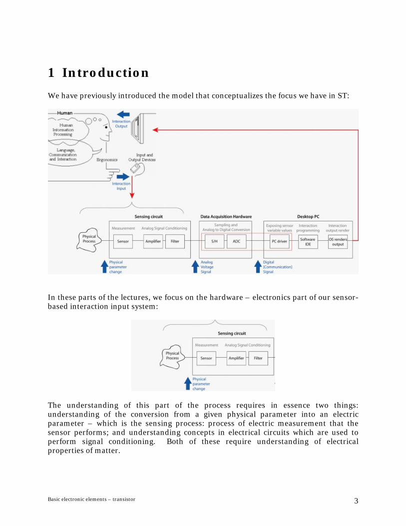
1 Introduction We have previously introduced the model that conceptualizes the focus we have in ST:
In these parts of the lectures, we focus on the hardware – electronics part of our sensor-based interaction input system:
The understanding of this part of the process requires in essence two things: understanding of the conversion from a given physical parameter into an electric parameter – which is the sensing process: process of electric measurement that the sensor performs; and understanding concepts in electrical circuits which are used to perform signal conditioning. Both of these require understanding of electrical properties of matter.
Basic electronic elements – transistor 3
So far, we have discussed circuit theory analysis of resistive circuits - and among them, sensor resistive circuits as well. We have also looked at the capacitor as a non-ohmic element, its influence in an electric circuit and the possibilities to use it in a sensor context. We have also looked at the diode (PN junction) as a semiconductor element. We now continue introducing basic electronic elements - this lecture is concerned with discussing the transistor. The transistor too is a semiconductor element. Special types of transistors also can be applied as sensor devices - these will be briefly introduced as well.
Basic electronic elements – transistor 4
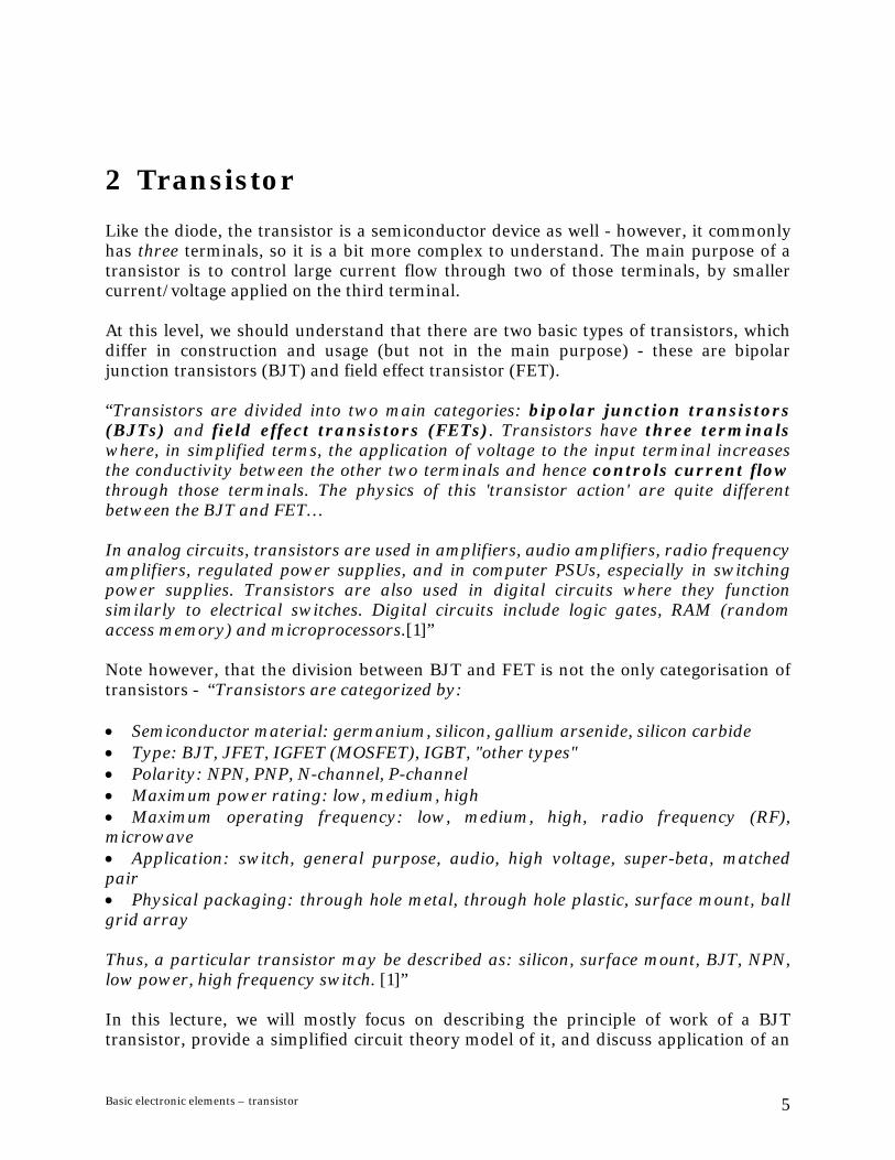
2 Transistor Like the diode, the transistor is a semiconductor device as well - however, it commonly has three terminals, so it is a bit more complex to understand. The main purpose of a transistor is to control large current flow through two of those terminals, by smaller current/voltage applied on the third terminal. At this level, we should understand that there are two basic types of transistors, which differ in construction and usage (but not in the main purpose) - these are bipolar junction transistors (BJT) and field effect transistor (FET). “Transistors are divided into two main categories: bipolar junction transistors (BJTs) and field effect transistors (FETs). Transistors have three terminals where, in simplified terms, the application of voltage to the input terminal increases the conductivity between the other two terminals and hence controls current flow through those terminals. The physics of this 'transistor action' are quite different between the BJT and FET… In analog circuits, transistors are used in amplifiers, audio amplifiers, radio frequency amplifiers, regulated power supplies, and in computer PSUs, especially in switching power supplies. Transistors are also used in digital circuits where they function similarly to electrical switches. Digital circuits include logic gates, RAM (random access memory) and microprocessors.[1]” Note however, that the division between BJT and FET is not the only categorisation of transistors - “Transistors are categorized by: • Semiconductor material: germanium, silicon, gallium arsenide, silicon carbide • Type: BJT, JFET, IGFET (MOSFET), IGBT, "other types" • Polarity: NPN, PNP, N-channel, P-channel • Maximum power rating: low, medium, high • Maximum operating frequency: low, medium, high, radio frequency (RF), microwave • Application: switch, general purpose, audio, high voltage, super-beta, matched pair • Physical packaging: through hole metal, through hole plastic, surface mount, ball grid array Thus, a particular transistor may be described as: silicon, surface mount, BJT, NPN, low power, high frequency switch. [1]” In this lecture, we will mostly focus on describing the principle of work of a BJT transistor, provide a simplified circuit theory model of it, and discuss application of an
Basic electronic elements – transistor 5

NPN BJT (as the calculations with it are easier) in several basic circuits. We will not go in further details of transistor design and analysis, which in itself is a rather complex area; we are only briefly going to mention FETs.
3 Bipolar junction transistor (BJT) The following excerpt gives a good introduction to BJTs: “The bipolar junction transistor (BJT) was the first type of transistor to be commercially mass-produced. Bipolar transistors are so named because conduction channel uses both majority and minority carriers for main electric current. The terminals are named emitter, base and collector. Two p-n junctions exist inside the BJT, collector-base junction and base-emitter junction. It is commonly described as a current operated device because the collector current is controlled by the current flowing between base and emitter terminals. [1]” Note that in a P semiconductor, majority carriers are holes, and minority carriers are free electrons; in a N semiconductor, majority carriers are free electrons, and minority carriers are holes. As an introduction, let’s include the following excerpt: “A BJT consists of three differently doped semiconductor regions, the emitter region, the base region and the collector region. These regions are, respectively, p type, n type and p type in a PNP transistor, and n type, p type and n type in a NPN transistor. Each semiconductor region is connected to a terminal, appropriately labeled: emitter (E), base (B) and collector (C).
Figure 1. Simplified cross-section of an npn BJT (left), closeup of a transistor (right) (Ref. [2])
The base is physically located between the emitter and the collector and is made from lightly doped, high resistivity material. The collector surrounds the emitter region, making it almost impossible for the electrons injected into the base region to escape
Basic electronic elements – transistor 6
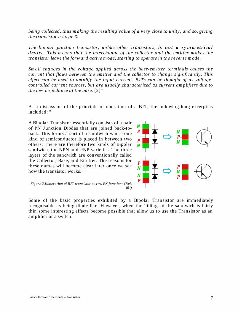
being collected, thus making the resulting value of a very close to unity, and so, giving the transistor a large ß. The bipolar junction transistor, unlike other transistors, is not a symmetrical device. This means that the interchange of the collector and the emitter makes the transistor leave the forward active mode, starting to operate in the reverse mode. Small changes in the voltage applied across the base-emitter terminals causes the current that flows between the emitter and the collector to change significantly. This effect can be used to amplify the input current. BJTs can be thought of as voltage-controlled current sources, but are usually characterized as current amplifiers due to the low impedance at the base. [2]” As a discussion of the principle of operation of a BJT, the following long excerpt is included: " A Bipolar Transistor essentially consists of a pair of PN Junction Diodes that are joined back-to-back. This forms a sort of a sandwich where one kind of semiconductor is placed in between two others. There are therefore two kinds of Bipolar sandwich, the NPN and PNP varieties. The three layers of the sandwich are conventionally called the Collector, Base, and Emitter. The reasons for these names will become clear later once we see how the transistor works.
Figure 2.Illustration of BJT transistor as two PN junctions (Ref. [6])
Some of the basic properties exhibited by a Bipolar Transistor are immediately recognisable as being diode-like. However, when the 'filling' of the sandwich is fairly thin some interesting effects become possible that allow us to use the Transistor as an amplifier or a switch.
Basic electronic elements – transistor 7
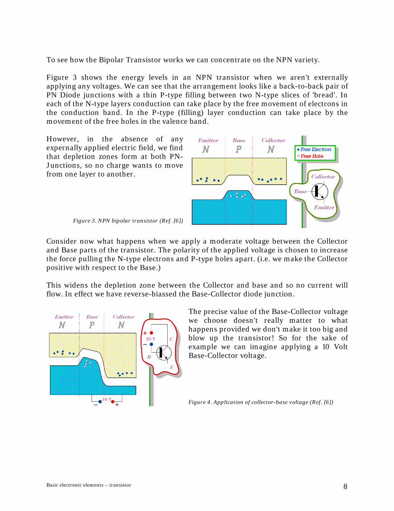
To see how the Bipolar Transistor works we can concentrate on the NPN variety. Figure 3 shows the energy levels in an NPN transistor when we aren't externally applying any voltages. We can see that the arrangement looks like a back-to-back pair of PN Diode junctions with a thin P-type filling between two N-type slices of 'bread'. In each of the N-type layers conduction can take place by the free movement of electrons in the conduction band. In the P-type (filling) layer conduction can take place by the movement of the free holes in the valence band. However, in the absence of any expernally applied electric field, we find that depletion zones form at both PN-Junctions, so no charge wants to move from one layer to another.
Figure 3. NPN bipolar transistor (Ref. [6])
Consider now what happens when we apply a moderate voltage between the Collector and Base parts of the transistor. The polarity of the applied voltage is chosen to increase the force pulling the N-type electrons and P-type holes apart. (i.e. we make the Collector positive with respect to the Base.) This widens the depletion zone between the Collector and base and so no current will flow. In effect we have reverse-biassed the Base-Collector diode junction.
The precise value of the Base-Collector voltage we choose doesn't really matter to what happens provided we don't make it too big and blow up the transistor! So for the sake of example we can imagine applying a 10 Volt Base-Collector voltage. Figure 4. Application of collector-base voltage (Ref. [6])
Basic electronic elements – transistor 8
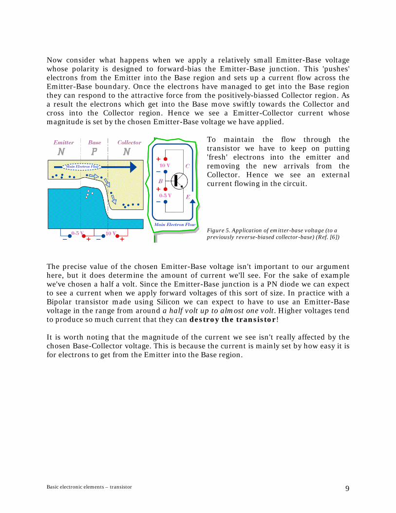
Now consider what happens when we apply a relatively small Emitter-Base voltage whose polarity is designed to forward-bias the Emitter-Base junction. This 'pushes' electrons from the Emitter into the Base region and sets up a current flow across the Emitter-Base boundary. Once the electrons have managed to get into the Base region they can respond to the attractive force from the positively-biassed Collector region. As a result the electrons which get into the Base move swiftly towards the Collector and cross into the Collector region. Hence we see a Emitter-Collector current whose magnitude is set by the chosen Emitter-Base voltage we have applied.
To maintain the flow through the transistor we have to keep on putting 'fresh' electrons into the emitter and removing the new arrivals from the Collector. Hence we see an external current flowing in the circuit. Figure 5. Application of emitter-base voltage (to a previously reverse-biased collector-base) (Ref. [6])
The precise value of the chosen Emitter-Base voltage isn't important to our argument here, but it does determine the amount of current we'll see. For the sake of example we've chosen a half a volt. Since the Emitter-Base junction is a PN diode we can expect to see a current when we apply forward voltages of this sort of size. In practice with a Bipolar transistor made using Silicon we can expect to have to use an Emitter-Base voltage in the range from around a half volt up to almost one volt. Higher voltages tend to produce so much current that they can destroy the transistor! It is worth noting that the magnitude of the current we see isn't really affected by the chosen Base-Collector voltage. This is because the current is mainly set by how easy it is for electrons to get from the Emitter into the Base region.
Basic electronic elements – transistor 9
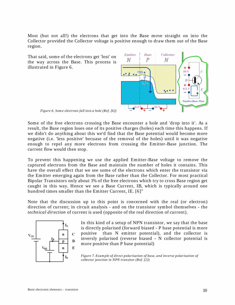
Most (but not all!) the electrons that get into the Base move straight on into the Collector provided the Collector voltage is positive enough to draw them out of the Base region. That said, some of the electrons get 'lost' on the way across the Base. This process is illustrated in Figure 6.
Figure 6. Some electrons fall into a hole (Ref. [6])
Some of the free electrons crossing the Base encounter a hole and 'drop into it'. As a result, the Base region loses one of its positive charges (holes) each time this happens. If we didn't do anything about this we'd find that the Base potential would become more negative (i.e. 'less positive' becuase of the removal of the holes) until it was negative enough to repel any more electrons from crossing the Emitter-Base junction. The current flow would then stop. To prevent this happening we use the applied Emitter-Base voltage to remove the captured electrons from the Base and maintain the number of holes it contains. This have the overall effect that we see some of the electrons which enter the transistor via the Emitter emerging again from the Base rather than the Collector. For most practical Bipolar Transistors only about 1% of the free electrons which try to cross Base region get caught in this way. Hence we see a Base Current, IB, which is typically around one hundred times smaller than the Emitter Current, IE. [6]" Note that the discussion up to this point is concerned with the real (or electron) direction of current; in circuit analysis - and on the transistor symbol themselves - the technical direction of current is used (opposite of the real direction of current).
In this kind of a setup of NPN transistor, we say that the base is directly polarised (forward biased - P base potential is more positive than N emitter potential), and the collector is inversly polarised (reverse biased - N collector potential is more positive than P base potential) Figure 7. Example of direct polarisation of base, and inverse polarisation of collector junction in NPN transitor (Ref. [2])
Basic electronic elements – transistor 10

Another representation of the conduction process in an NPN transistor is given below, this time through the technical direction of current:
Figure 8. Process of transistor conduction, illustarted with conventional (technical) direction of current. (Ref. [5] )
In an NPN transistor, electrons flow into the emitter, which is the real direction of current; so the technical (conventional) direction of emitter current will be out of the emitter. "Bipolar transistors, having 2 junctions, are 3 terminal semiconductor devices. The three terminals are emitter, collector, and base. A transistor can be either NPN or PNP. See the schematic representations below:
Figure 9. Schematic symbols of PNP and NPN BJT transistors (Ref. [6])
Note that the direction of the emitter arrow defines the type of transistor. Biasing and power supply polarity are positive for NPN and negative for PNP transistors. The transistor is primarily used as an current amplifier. When a small current signal is applied to the base terminal, it is amplified in the collector circuit. This current amplification is referred to as hFE or beta (β) and equals Ic/Ib. As with all semiconductors, breakdown voltage is a design limitation. There are breakdown voltages that must be taken into account for each combination of terminals. i.e. Vce, Vbe, and Vcb. However, Vce(collector-emitter voltage) with open base, designated as Vceo, is usually of most concern and defines the maximum circuit voltage.
Basic electronic elements – transistor 11
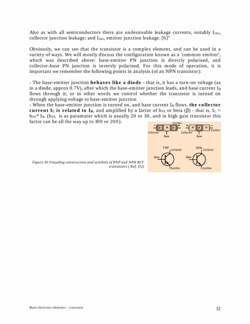
Also as with all semiconductors there are undesireable leakage currents, notably Icbo, collector junction leakage; and Iebo, emitter junction leakage. [6]" Obviously, we can see that the transistor is a complex element, and can be used in a variety of ways. We will mostly discuss the configuration known as a 'common emitter', which was described above: base-emitter PN junction is directly polarised, and collector-base PN junction is inversly polarised. For this mode of operation, it is important we remember the following points in analysis (of an NPN transistor): - The base-emitter junction behaves like a diode - that is, it has a turn-on voltage (as in a diode, approx 0.7V), after which the base-emitter junction leads, and base current IB flows through it; or in other words we control whether the transistor is turned on through applying voltage to base-emitter junction - When the base-emitter junction is turned on, and base current IB flows, the collector current IC is related to IB, and amplified by a factor of hFE or beta (β) - that is, IC = hFE* IB. (hFE is as paramater which is usually 20 or 30, and in high gain transistor this factor can be all the way up to 100 or 200).
Figure 10.Visualing construction and symbols of PNP and NPN BJT transistors ( Ref. [5])
Basic electronic elements – transistor 12
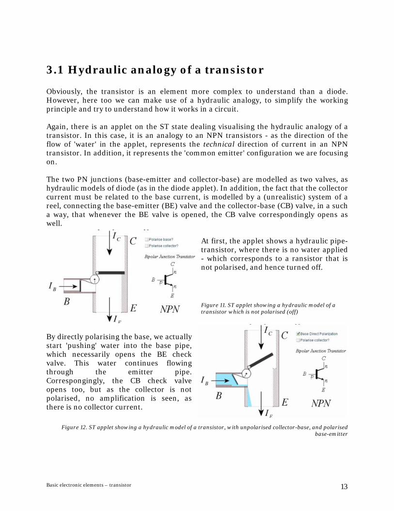
3.1 Hydraulic analogy of a transistor Obviously, the transistor is an element more complex to understand than a diode. However, here too we can make use of a hydraulic analogy, to simplify the working principle and try to understand how it works in a circuit. Again, there is an applet on the ST state dealing visualising the hydraulic analogy of a transistor. In this case, it is an analogy to an NPN transistors - as the direction of the flow of 'water' in the applet, represents the technical direction of current in an NPN transistor. In addition, it represents the 'common emitter' configuration we are focusing on. The two PN junctions (base-emitter and collector-base) are modelled as two valves, as hydraulic models of diode (as in the diode applet). In addition, the fact that the collector current must be related to the base current, is modelled by a (unrealistic) system of a reel, connecting the base-emitter (BE) valve and the collector-base (CB) valve, in a such a way, that whenever the BE valve is opened, the CB valve correspondingly opens as well.
At first, the applet shows a hydraulic pipe-transistor, where there is no water applied - which corresponds to a ransistor that is not polarised, and hence turned off. Figure 11. ST applet showing a hydraulic model of a transistor which is not polarised (off)
By directly polarising the base, we actually start 'pushing' water into the base pipe, which necessarily opens the BE check valve. This water continues flowing through the emitter pipe. Correspongingly, the CB check valve opens too, but as the collector is not polarised, no amplification is seen, as there is no collector current.
Figure 12. ST applet showing a hydraulic model of a transistor, with unpolarised collector-base, and polarised base-emitter
Basic electronic elements – transistor 13
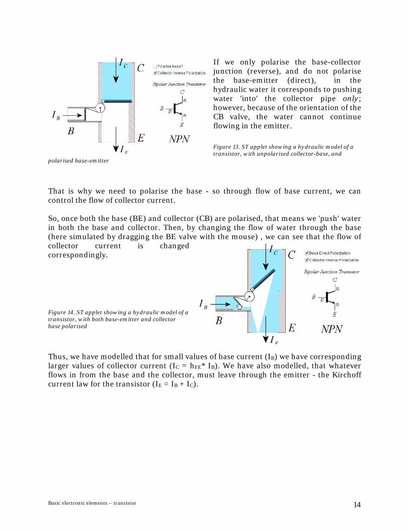
If we only polarise the base-collector junction (reverse), and do not polarise the base-emitter (direct), in the hydraulic water it corresponds to pushing water 'into' the collector pipe only; however, because of the orientation of the CB valve, the water cannot continue flowing in the emitter. Figure 13. ST applet showing a hydraulic model of a transistor, with unpolarised collector-base, and
polarised base-emitter
That is why we need to polarise the base - so through flow of base current, we can control the flow of collector current. So, once both the base (BE) and collector (CB) are polarised, that means we 'push' water in both the base and collector. Then, by changing the flow of water through the base (here simulated by dragging the BE valve with the mouse) , we can see that the flow of collector current is changed correspondingly. Figure 14. ST applet showing a hydraulic model of a transistor, with both base-emitter and collector base polarised
Thus, we have modelled that for small values of base current (IB) we have corresponding larger values of collector current (IC = hFE* IB). We have also modelled, that whatever flows in from the base and the collector, must leave through the emitter - the Kirchoff current law for the transistor (IE = IB + IC).
Basic electronic elements – transistor 14
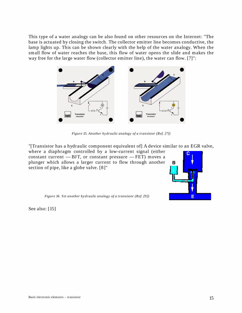
This type of a water analogy can be also found on other resources on the Internet: "The base is actuated by closing the switch. The collector emitter line becomes conductive, the lamp lights up. This can be shown clearly with the help of the water analogy. When the small flow of water reaches the base, this flow of water opens the slide and makes the way free for the large water flow (collector emitter line), the water can flow. [7]":
Figure 15. Another hydraulic analogy of a transistor (Ref. [7])
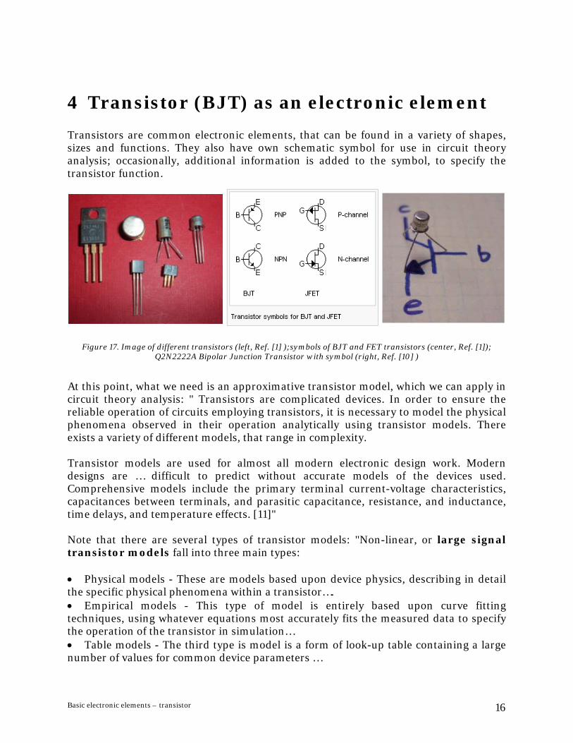
"[Transistor has a hydraulic component equivalent of] A device similar to an EGR valve, where a diaphragm controlled by a low-current signal (either constant current — BJT, or constant pressure — FET) moves a plunger which allows a larger current to flow through another section of pipe, like a globe valve. [8]"
Figure 16. Yet another hydraulic analogy of a transistor (Ref. [9])
See also: [15]
Basic electronic elements – transistor 15
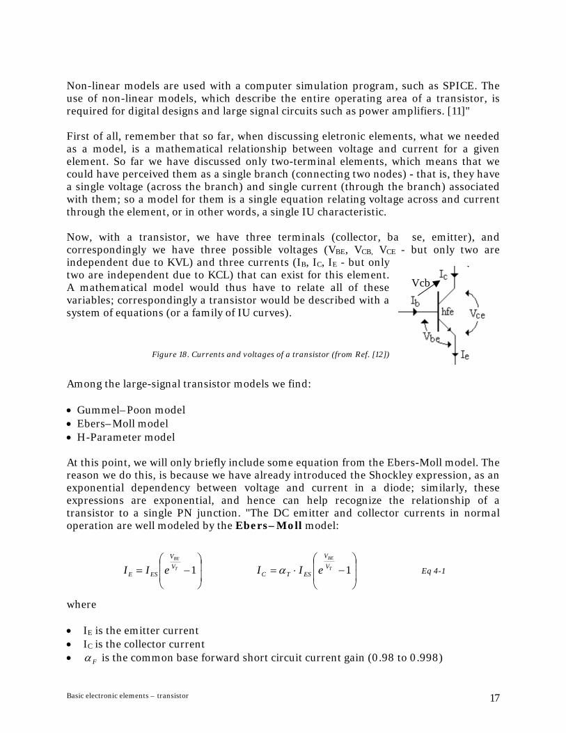
4 Transistor (BJT) as an electronic element Transistors are common electronic elements, that can be found in a variety of shapes, sizes and functions. They also have own schematic symbol for use in circuit theory analysis; occasionally, additional information is added to the symbol, to specify the transistor function.
Figure 17. Image of different transistors (left, Ref. [1] );symbols of BJT and FET transistors (center, Ref. [1]);
Q2N2222A Bipolar Junction Transistor with symbol (right, Ref. [10] )
At this point, what we need is an approximative transistor model, which we can apply in circuit theory analysis: " Transistors are complicated devices. In order to ensure the reliable operation of circuits employing transistors, it is necessary to model the physical phenomena observed in their operation analytically using transistor models. There exists a variety of different models, that range in complexity. Transistor models are used for almost all modern electronic design work. Modern designs are … difficult to predict without accurate models of the devices used. Comprehensive models include the primary terminal current-voltage characteristics, capacitances between terminals, and parasitic capacitance, resistance, and inductance, time delays, and temperature effects. [11]" Note that there are several types of transistor models: "Non-linear, or large signal transistor models fall into three main types: • Physical models - These are models based upon device physics, describing in detail the specific physical phenomena within a transistor…. • Empirical models - This type of model is entirely based upon curve fitting techniques, using whatever equations most accurately fits the measured data to specify the operation of the transistor in simulation… • Table models - The third type is model is a form of look-up table containing a large number of values for common device parameters …
Basic electronic elements – transistor 16
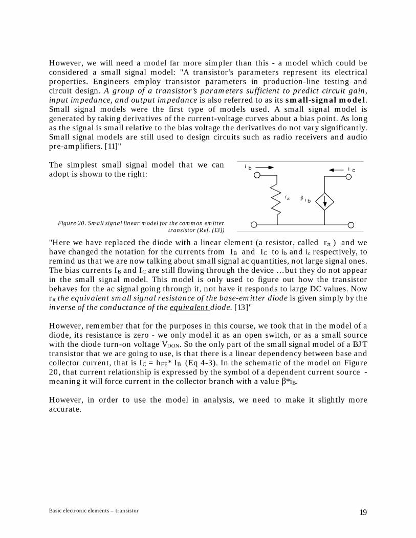
Non-linear models are used with a computer simulation program, such as SPICE. The use of non-linear models, which describe the entire operating area of a transistor, is required for digital designs and large signal circuits such as power amplifiers. [11]" First of all, remember that so far, when discussing eletronic elements, what we needed as a model, is a mathematical relationship between voltage and current for a given element. So far we have discussed only two-terminal elements, which means that we could have perceived them as a single branch (connecting two nodes) - that is, they have a single voltage (across the branch) and single current (through the branch) associated with them; so a model for them is a single equation relating voltage across and current through the element, or in other words, a single IU characteristic. Now, with a transistor, we have three terminals (collector, ba se, emitter), and correspondingly we have three possible voltages (VBE, VCB, VCE - but only two are independent due to KVL) and three currents (IB, IC, IE - but only two are independent due to KCL) that can exist for this element. A mathematical model would thus have to relate all of these variables; correspondingly a transistor would be described with a system of equations (or a family of IU curves).
Vcb
Figure 18. Currents and voltages of a transistor (from Ref. [12])
Among the large-signal transistor models we find: • Gummel–Poon model • Ebers–Moll model • H-Parameter model At this point, we will only briefly include some equation from the Ebers-Moll model. The reason we do this, is because we have already introduced the Shockley expression, as an exponential dependency between voltage and current in a diode; similarly, these expressions are exponential, and hence can help recognize the relationship of a transistor to a single PN junction. "The DC emitter and collector currents in normal operation are well modeled by the Ebers–Moll model:
⎟⎟
⎠
⎞
⎜⎜
⎝
⎛−= 1T
EB
VV
ESE eII ⎟⎟
⎠
⎞
⎜⎜
⎝
⎛−⋅= 1T
EB
VV
ESTC eII α Eq 4-1
where • IE is the emitter current • IC is the collector current • Fα is the common base forward short circuit current gain (0.98 to 0.998)
Basic electronic elements – transistor 17

• IES is the reverse saturation current of the base-emitter diode (on the order of 10-15
to 10-12 amperes) • VT is the thermal voltage kT/q (approximately 26 mV at room temperature ˜ 300 K). • VBE is the base-emitter voltage • Fβ (aka hFE) is current gain - the ratio of the allowed collector-emitter current to the base-emitter current. The collector current is slightly less than the emitter current, since the value of αT is very close to 1.0. In the BJT a small amount of base–emitter current causes a larger amount of collector–emitter current. The ratio of the allowed collector–emitter current to the base–emitter current is called current gain, β or hFE. A β value of 100 is typical for small bipolar transistors. In a typical configuration, a very small signal current flows through the base–emitter junction to control the emitter–collector current. β is related to α through the following relations:
ETC II ⋅= α Eq 4-2
BFC II ⋅= β Eq 4-3
T
TF α
αβ−
=1
Eq 4-4
[2]" Note that a typical transistor characteristic is given as a family of curves, which show certain voltage-current characteristics for a pair of terminals, obtained when a parameter of a third terminal is changed. A typical collector characteristic curve - dependence of Ic on Uce, when Ib is changed - is shown here:
Figure 19. Typical collector characteristic curve for a transistor (Ref. [6])
Basic electronic elements – transistor 18
However, we will need a model far more simpler than this - a model which could be considered a small signal model: "A transistor’s parameters represent its electrical properties. Engineers employ transistor parameters in production-line testing and circuit design. A group of a transistor’s parameters sufficient to predict circuit gain, input impedance, and output impedance is also referred to as its small-signal model. Small signal models were the first type of models used. A small signal model is generated by taking derivatives of the current-voltage curves about a bias point. As long as the signal is small relative to the bias voltage the derivatives do not vary significantly. Small signal models are still used to design circuits such as radio receivers and audio pre-amplifiers. [11]" The simplest small signal model that we can adopt is shown to the right:
Figure 20. Small signal linear model for the common emitter transistor (Ref. [13])
"Here we have replaced the diode with a linear element (a resistor, called rπ ) and we have changed the notation for the currents from IB and IC to ib and ic respectively, to remind us that we are now talking about small signal ac quantities, not large signal ones. The bias currents IB and IC are still flowing through the device … but they do not appear in the small signal model. This model is only used to figure out how the transistor behaves for the ac signal going through it, not have it responds to large DC values. Now rπ the equivalent small signal resistance of the base-emitter diode is given simply by the inverse of the conductance of the equivalent diode. [13]" However, remember that for the purposes in this course, we took that in the model of a diode, its resistance is zero - we only model it as an open switch, or as a small source with the diode turn-on voltage VDON. So the only part of the small signal model of a BJT transistor that we are going to use, is that there is a linear dependency between base and collector current, that is IC = hFE* IB (Eq 4-3). In the schematic of the model on Figure 20, that current relationship is expressed by the symbol of a dependent current source - meaning it will force current in the collector branch with a value β*iB. However, in order to use the model in analysis, we need to make it slightly more accurate.
Basic electronic elements – transistor 19
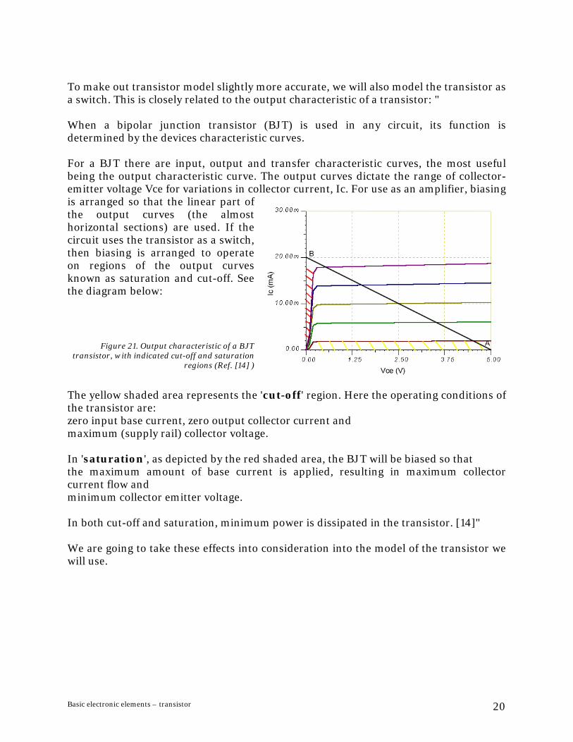
To make out transistor model slightly more accurate, we will also model the transistor as a switch. This is closely related to the output characteristic of a transistor: " When a bipolar junction transistor (BJT) is used in any circuit, its function is determined by the devices characteristic curves. For a BJT there are input, output and transfer characteristic curves, the most useful being the output characteristic curve. The output curves dictate the range of collector-emitter voltage Vce for variations in collector current, Ic. For use as an amplifier, biasing is arranged so that the linear part of the output curves (the almost horizontal sections) are used. If the circuit uses the transistor as a switch, then biasing is arranged to operate on regions of the output curves known as saturation and cut-off. See the diagram below:
Figure 21. Output characteristic of a BJT transistor, with indicated cut-off and saturation
regions (Ref. [14] )
The yellow shaded area represents the 'cut-off' region. Here the operating conditions of the transistor are: zero input base current, zero output collector current and maximum (supply rail) collector voltage. In 'saturation', as depicted by the red shaded area, the BJT will be biased so that the maximum amount of base current is applied, resulting in maximum collector current flow and minimum collector emitter voltage. In both cut-off and saturation, minimum power is dissipated in the transistor. [14]" We are going to take these effects into consideration into the model of the transistor we will use.
Basic electronic elements – transistor 20
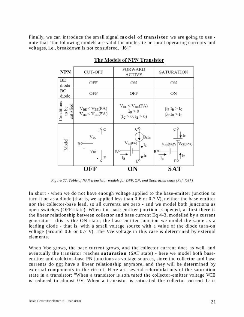
Finally, we can introduce the small signal model of transistor we are going to use - note that "the following models are valid for moderate or small operating currents and voltages, i.e., breakdown is not considered. [16]"
ON SAT OFF
Figure 22. Table of NPN transistor models for OFF, ON, and Saturation state (Ref. [16] )
In short - when we do not have enough voltage applied to the base-emitter junction to turn it on as a diode (that is, we applied less than 0.6 or 0.7 V), neither the base-emitter nor the collector-base lead, so all currents are zero - and we model both junctions as open switches (OFF state). When the base-emitter junction is opened, at first there is the linear relationship between collector and base current Eq 4-3, modelled by a current generator - this is the ON state; the base-emitter junction we model the same as a leading diode - that is, with a small voltage source with a value of the diode turn-on voltage (around 0.6 or 0.7 V). The Vce voltage in this case is determined by external elements. When Vbe grows, the base current grows, and the collector current does as well, and eventually the transistor reaches saturation (SAT state) - here we model both base-emitter and colelctor-base PN junctions as voltage sources, since the collector and base currents do not have a linear relationship anymore, and they will be determined by external components in the circuit. Here are several reformulations of the saturation state in a transistor: "When a transistor is saturated the collector-emitter voltage VCE is reduced to almost 0V. When a transistor is saturated the collector current Ic is
Basic electronic elements – transistor 21

determined by the supply voltage and the external resistance in the collector circuit, not by the transistor's current gain. [18]". Also "generally if you apply enough base current that the maximum current possible will always flow, then the transistor is operating like a switch (rather than operating like an amplifier). In this mode, the transistor is said to be saturated. … A BJT transistor will cause a drop in voltage between the collector and the emitter even when it is saturated (it isn't a perfect conductor). This voltage drop is called out in the data sheet as Vce(sat). Typically, this will be between .2 and 1 volts for silicon transistors. [19]" "For active operation, the collector-base junction must be reversed biased (positive Vcb). Once Vcb enters the -.5V ballpark it ceases to be reversed biased, and the collector current now depends on Vcb. Practically speaking this provides an output voltage minimum for Vce [which is VceSAT] [27]" Figure 23.Common saturation voltage range of an NPN transistor (Ref. [27])
This is also included in the following excerpt: "The Bipolar Junction Transistor (BJT) is an active device. In simple terms, it is a current controlled valve. The base current (IB) controls the collector current (IC).
Regions of BJT operation:
Cut-off region: The transistor is off. There is no conduction between the collector and the emitter. (IB = 0 therefore IC = 0)
Active region: The transistor is on. The collector current is proportional to and controlled by the base current (IC = βIB) and relatively insensitive to VCE. In this region the transistor can be an amplifier.
Saturation region: The transistor is on. The collector current varies very little with a change in the base current in the saturation region. The VCE is small, a few tenths of volt. The collector current is strongly dependent on VCE unlike in the active region. It is desirable to operate transistor switches will be in or near the saturation region when in their on state.
Rules for Bipolar Junction Transistors (BJTs):
• For an npn transistor, the voltage at the collector VC must be greater than the voltage at the emitter VE by at least a few tenths of a volt; otherwise, current will not flow through the collector-emitter junction, no matter what the applied voltage at the base.
Basic electronic elements – transistor 22
• For the npn transistor, there is a voltage drop from the base to the emitter of 0.6 V. In terms of operation, this means that the base voltage VB of an npn transistor must be at least 0.6 V greater that the emitter voltage VE; otherwise, the transistor will not pass emitter-to-collector current. [17]"
So, for this kind of a model, all we need are the basic equations of the BJT, below.
Figure 24. Basic equations of the BJT in our simplified model (Ref. [17] )
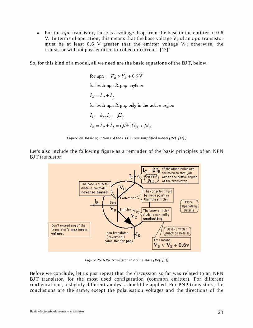
Let's also include the following figure as a reminder of the basic principles of an NPN BJT transistor:
Figure 25. NPN transistor in active state (Ref. [5])
Before we conclude, let us just repeat that the discussion so far was related to an NPN BJT transistor, for the most used configuration (common emitter). For different configurations, a slightly different analysis should be applied. For PNP transistors, the conclusions are the same, except the polarisation voltages and the directions of the
Basic electronic elements – transistor 23

currents are going to be reversed, in respect to NPN transistors. (Note that most of the resources included in this document discuss both NPN and PNP transistors).
Basic electronic elements – transistor 24
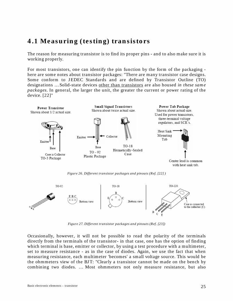
4.1 Measuring (testing) transistors The reason for measuring transistor is to find its proper pins - and to also make sure it is working properly. For most transistors, one can identify the pin function by the form of the packaging - here are some notes about transistor packages: "There are many transistor case designs. Some conform to JEDEC Standards and are defined by Transistor Outline (TO) designations … Solid-state devices other than transistors are also housed in these same packages. In general, the larger the unit, the greater the current or power rating of the device. [22]"
Figure 26. Different transistor packages and pinouts (Ref. [22] )
Figure 27. Different transistor packages and pinouts (Ref. [23])
Occasionally, however, it will not be possible to read the polarity of the terminals directly from the terminals of the transistor- in that case, one has the option of finding which terminal is base, emitter or collector, by using a test procedure with a multimeter, set to measure resistance - as in the case of diodes. Again, we use the fact that when measuring resistance, each multimeter 'becomes' a small voltage source. This would be the ohmmeters view of the BJT: "Clearly a transistor cannot be made on the bench by combining two diodes. … Most ohmmeters not only measure resistance, but also
Basic electronic elements – transistor 25
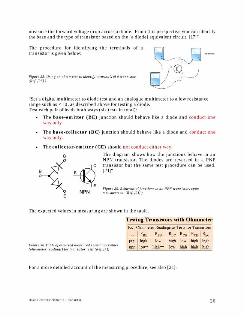
measure the forward voltage drop across a diode. From this perspective you can identify the base and the type of transistor based on the [a diode] equivalent circuit. [17]" The procedure for identifying the terminals of a transistor is given below: Figure 28. Using an ohmmeter to identify terminals of a transistor (Ref. [26] )
"Set a digital multimeter to diode test and an analogue multimeter to a low resistance range such as × 10, as described above for testing a diode. Test each pair of leads both ways (six tests in total):
• The base-emitter (BE) junction should behave like a diode and conduct one way only.
• The base-collector (BC) junction should behave like a diode and conduct one way only.
• The collector-emitter (CE) should not conduct either way.
The diagram shows how the junctions behave in an NPN transistor. The diodes are reversed in a PNP transistor but the same test procedure can be used. [21]" Figure 29. Behavior of junctions in an NPN transistor, upon measurement (Ref. [21] )
The expected values in measuring are shown in the table.
Figure 30.Table of expected measured resistance values (ohmmeter readings) for transistor tests (Ref. [4])
For a more detailed account of the measuring procedure, see also [21].
Basic electronic elements – transistor 26
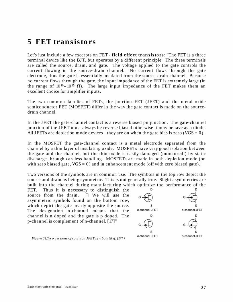
5 FET transistors Let's just include a few excerpts on FET - field effect transistors: "The FET is a three terminal device like the BJT, but operates by a different principle. The three terminals are called the source, drain, and gate. The voltage applied to the gate controls the current flowing in the source-drain channel. No current flows through the gate electrode, thus the gate is essentially insulated from the source-drain channel. Because no current flows through the gate, the input impedance of the FET is extremely large (in the range of 1010–1015 Ω). The large input impedance of the FET makes them an excellent choice for amplifier inputs. The two common families of FETs, the junction FET (JFET) and the metal oxide semiconductor FET (MOSFET) differ in the way the gate contact is made on the source-drain channel. In the JFET the gate-channel contact is a reverse biased pn junction. The gate-channel junction of the JFET must always be reverse biased otherwise it may behave as a diode. All JFETs are depletion mode devices—they are on when the gate bias is zero (VGS = 0). In the MOSFET the gate-channel contact is a metal electrode separated from the channel by a thin layer of insulating oxide. MOSFETs have very good isolation between the gate and the channel, but the thin oxide is easily damaged (punctured!) by static discharge through careless handling. MOSFETs are made in both depletion mode (on with zero biased gate, VGS = 0) and in enhancement mode (off with zero biased gate). Two versions of the symbols are in common use. The symbols in the top row depict the source and drain as being symmetric. This is not generally true. Slight asymmetries are built into the channel during manufacturing which optimize the performance of the FET. Thus it is necessary to distinguish the source from the drain. [] We will use the asymmetric symbols found on the bottom row, which depict the gate nearly opposite the source. The designation n-channel means that the channel is n doped and the gate is p doped. The p-channel is complement of n-channel. [17]"
Figure 31.Two versions of common JFET symbols (Ref. [17] )
Basic electronic elements – transistor 27

6 Transistor construction Transistors, like diodes, are produced using a variety of chemical processes. All of these elements are made by different combinations of P and N semiconductor - a visual overview of the differences in construction are provided below:
Figure 32.Differences in construction of semiconductor elements (Ref. [25])
A very good illustration of the transistor - both BJT and FET - fabrication process is given in [24].
Figure 33. Cross-section of a semiconductor FET and BJT transistor (Ref. [24] )
Basic electronic elements – transistor 28
7 Basic circuits In this section, we analyze several basic circuits that are based on the functionality of a BJT NPN transistor.
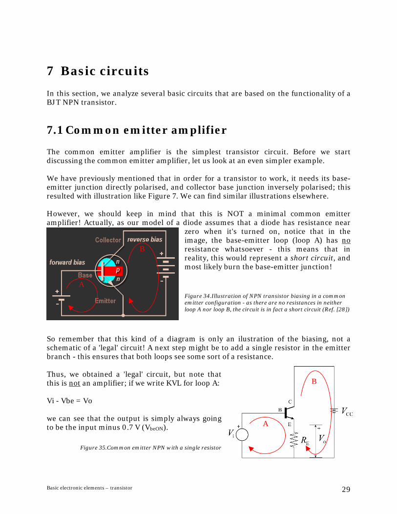
7.1 Common emitter amplifier The common emitter amplifier is the simplest transistor circuit. Before we start discussing the common emitter amplifier, let us look at an even simpler example. We have previously mentioned that in order for a transistor to work, it needs its base-emitter junction directly polarised, and collector base junction inversely polarised; this resulted with illustration like Figure 7. We can find similar illustrations elsewhere. However, we should keep in mind that this is NOT a minimal common emitter amplifier! Actually, as our model of a diode assumes that a diode has resistance near
zero when it's turned on, notice that in the image, the base-emitter loop (loop A) has no resistance whatsoever - this means that in reality, this would represent a short circuit, and most likely burn the base-emitter junction!
B
A Figure 34.Illustration of NPN transistor biasing in a common emitter configuration - as there are no resistances in neither loop A nor loop B, the circuit is in fact a short circuit (Ref. [28])
So remember that this kind of a diagram is only an ilustration of the biasing, not a schematic of a 'legal' circuit! A next step might be to add a single resistor in the emitter branch - this ensures that both loops see some sort of a resistance.
B
A
Thus, we obtained a 'legal' circuit, but note that this is not an amplifier; if we write KVL for loop A: Vi - Vbe = Vo we can see that the output is simply always going to be the input minus 0.7 V (VbeON).
Figure 35.Common emitter NPN with a single resistor
Basic electronic elements – transistor 29
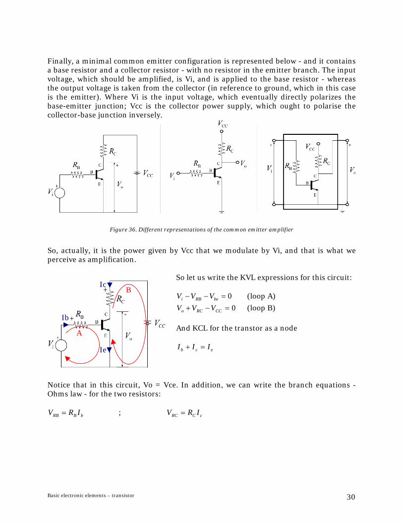
Finally, a minimal common emitter configuration is represented below - and it contains a base resistor and a collector resistor - with no resistor in the emitter branch. The input voltage, which should be amplified, is Vi, and is applied to the base resistor - whereas the output voltage is taken from the collector (in reference to ground, which in this case is the emitter). Where Vi is the input voltage, which eventually directly polarizes the base-emitter junction; Vcc is the collector power supply, which ought to polarise the collector-base junction inversely.
Figure 36. Different representations of the common emitter amplifier
So, actually, it is the power given by Vcc that we modulate by Vi, and that is what we perceive as amplification.
So let us write the KVL expressions for this circuit:
A
+
Ie
Ic +
Ib
B 0=−− beRBi VVV (loop A)
0=−+ CCRCo VVV (loop B)
And KCL for the transtor as a node
ecb III =+
Notice that in this circuit, Vo = Vce. In addition, we can write the branch equations - Ohms law - for the two resistors:
bBRB IRV = ; cCRC IRV =
Basic electronic elements – transistor 30

From loop A we can express the base-emitter voltage:
bBiRBibe IRVVVV −=−=
If this voltage is less than the turn-on voltage of base-emitter junction (assumed 0.6V), then the transistor is OFF. If it is greater then 0.6V, then the transistor turns on. We can express this differently - if we express the current Ib (from KVL for loop A):
B
beib R
VVI
−=
From here, as Vbe keeps a value of around 0.6V when the transistor is ON, the input voltage Vi must be at least greater than 0.6V, so we have positive base current (flowing into the base) so to turn the transistor ON. Once the transistor is turned on, while in the active state, we additionally have the linear relationship between collector and base current:
bFEc IhI ⋅=
In this state, we can directly express the relationship between input and output voltage - from KVL for loop B:
bFECCCcCCCRCCCo IhRVIRVVVV −=−=−=
( ) ( )6.0−−≈−−= iB
CFECCbei
B
CFECCo V
RRhVVV
RRhVV
From here, we can see that the output voltage Vo (in this case Vce as well) is maximum when the input voltage is <= 0.6; before the transistor turns on, the output voltage Vo = Vcc. As Vi grows, Vo (which is also Vce) drops (gets smaller); and this is the case as long as the transistor stays in the active state. However, as Vi grows, the base current grows as well, so does the collector current, and the transistor eventually goes in saturation (SAT). For saturation, the linear dependancy between base and collector current is not valid anymore, and we know that Vce reaches the value of VceSAT for that transistor - typically some 0.2 V. Thus, in saturation, the collector current will be fixed on:
C
CC
C
ceSATCC
C
oCCc R
VR
VVR
VVI
2.0max
−≈
−=
−=
Basic electronic elements – transistor 31

The corresponding maximum base current, at the moment of transition between ON and SAT will be:
CFE
CC
FE
cb Rh
VhI
I2.0max
max−
≈=
And so the input voltage when the transistor crosses into saturation is
6.02.0
6.0maxmax +−
=+≈+=CFE
CCBbBbeRBi Rh
VRIRVVV
Of course, as here the output voltage is the collector-emitter voltage, so the output voltage in saturation will be Vo = VceSAT = 0.2V. So, now we have the ranges of our analysis: Vi < 0.6V -> T is OFF -> Vo = Vcc
0.6V < Vi < 6.02.0
+−
CFE
CCB Rh
VR -> T is ON -> ( )6.0−−= i
B
CFECCo V
RRh
VV
Vi > 6.02.0
+−
CFE
CCB Rh
VR -> T is SAT -> Vo = 0.2V
Now, if we have Vcc = 5V, hFE = 100, and RC = RB, we obtain: Vi < 0.6V -> T is OFF -> Vo = 5V 0.6V < Vi < 0.648 -> T is ON -> Vo = 65 - 100*Vi (5 > Vo > 0.2) Vi > 0.648 -> T is SAT -> Vo = 0.2 V Notice for a voltage change from 0.6 to 0.648 V (total change = 0.048V) we got a swing from 5 to 0.2 V (total change = - 4.8 V). So the obtained change of output voltage is about 100 times greater than the change of the input voltage - hence we obtained amplification. We can express change through the delta operator, and apply it to the equation relating input and output voltage:
( 6.0−−≈ iB
CFECCo V
RRhVV ) / delta differentiate
iB
CFEo V
RRhV ∆−≈∆
Basic electronic elements – transistor 32
So, an amplification factor can be calculated as the relationship between output and input change of voltage:
B
CFE
i
o
RRh
VVA −≈
∆∆
=
And it only depends on the transistor current gain parameter hFE (or β), and the values of the resistors. If Rc=Rb, then it solely depends on hFE, and knowing that a typical hFE is between 50 and 200 - that means with a typical transistor in this configuration we'd get between 50 and 200 factor of voltage amplification. ------------------------------- Notice that in this simple case, one cannot simply amplify an AC signal (which typically goes from negative to positive voltages, centered around the zero). That is because we need at least 0.6V to have the transistor turn on. In this case, to analyse our circuit we can only use an AC signal changing from 0.6V to 0.648V; this can be modelled with a DC generator, and a zero centered AC signal: The amplitude of the AC signal is ( 0.648 - 0.6 ) /2 = 0.024 V The DC generator should have the central value ( 0.648 + 0.6 ) /2 = 0.624 V So, our signal can be modelled with
( )tVi ωsin024.0624.0 ⋅+=
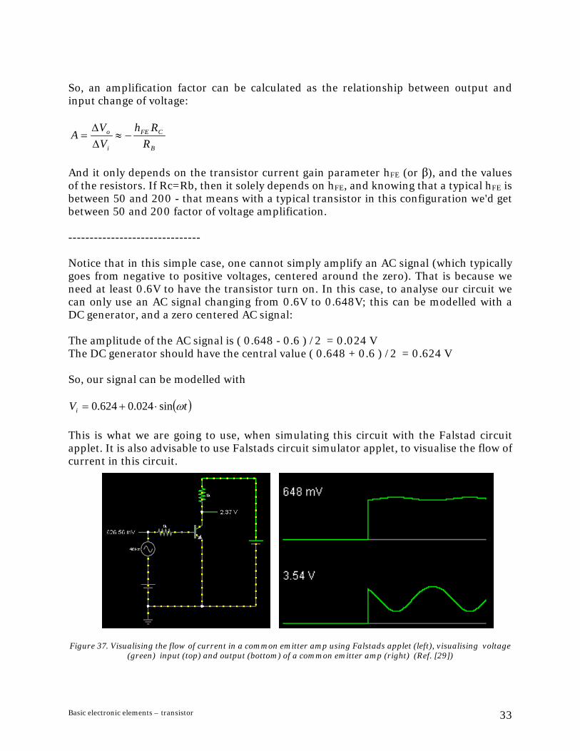
This is what we are going to use, when simulating this circuit with the Falstad circuit applet. It is also advisable to use Falstads circuit simulator applet, to visualise the flow of current in this circuit. Figure 37. Visualising the flow of current in a common emitter amp using Falstads applet (left), visualising voltage
(green) input (top) and output (bottom) of a common emitter amp (right) (Ref. [29])
Basic electronic elements – transistor 33
Note that in the Falstad simulator, the parameters of the transistor cannot be changed. However, it is obvious by comparing the input and output signal, that the input signal as been amplified - but also, the input is in counter-phase with the output voltage (when the input voltage grows, the output drops and vice versa). Notice that the applet has the finetuned voltage described above, so a clean sinusoid is obtained on the output - this means the transistor works all the time in the active state (ON). Try changing the DC and the AC component of the voltage component, to see how soon the transistor will start going into either OFF or SAT, and thereby distort the signal. ----------------- Note finally, that for practical applications, this simplest form of the common emitter amplifier is rarely used. A more common, practical form of the common emitter amplifier is shown below.
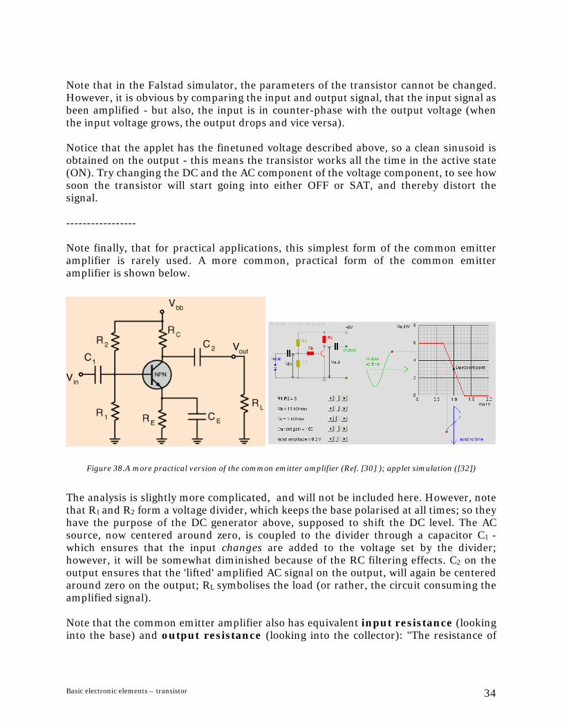
Figure 38.A more practical version of the common emitter amplifier (Ref. [30] ); applet simulation ([32])
The analysis is slightly more complicated, and will not be included here. However, note that R1 and R2 form a voltage divider, which keeps the base polarised at all times; so they have the purpose of the DC generator above, supposed to shift the DC level. The AC source, now centered around zero, is coupled to the divider through a capacitor C1 - which ensures that the input changes are added to the voltage set by the divider; however, it will be somewhat diminished because of the RC filtering effects. C2 on the output ensures that the 'lifted' amplified AC signal on the output, will again be centered around zero on the output; RL symbolises the load (or rather, the circuit consuming the amplified signal). Note that the common emitter amplifier also has equivalent input resistance (looking into the base) and output resistance (looking into the collector): "The resistance of
Basic electronic elements – transistor 34
the input loop is the base resistance in series with the resistance in the emitter-side of the circuit, referred to the base by the β transform.
( ) ( EEBin RrRCEr +⋅++= )β1)(
At the output node, the BJT transistor model shows a current source (infinite resistance) in parallel with load resistance RL. The output resistance is therefore RL. The CE amplifier has relatively high input resistance due to the β -transform effect at the base. It is better as a voltage-input port. Its output resistance is relatively low if the load resistor is not made too large. [35]" Note that in the previous simple case, RE was zero, so this effect of increase of input resistance due to hFE could not be seen. For more on the common-emitter amplifier, see [30], [31], [32], [33], [34] … ---------------------------------------------- Note that when talking about powering transistors, some special notation is used for the supplies: "VCC (note: lower case is often used instead of subscript, e.g. 'Vcc') is an electronics designation that refers to voltage from a power supply connected to the 'collector' terminal of a bipolar transistor. In an NPN bipolar junction transistor, it would be +VCC, while in a PNP transistor, it would be −VCC. There is debate over the origins of the double letter subscript naming convention. One proposal is that it originated as an abbreviation of the supply voltage for a common collector amplifier with the other power supply names mimicking this fashion. Double letters may also have been used to clearly indicate that a power supply voltage is being referred to. [37]"
Basic electronic elements – transistor 35
7.2 Current source and current mirror So far we have mostly discussed voltage sources as power supplies (emf generators) in a circuit - their job is to keep constant potential difference on their ends; which means they adjust the current that flows through them depending on the total resistance of the circuit. We haven't so far discussed the other types of sources - current sources; which try to maintain constant current, whereas the voltage is set by the resistance of the rest of the circuit.
A very simple way of implementing a current source, is simply biasing a common emitter transistor permanently; as the base current is fixed, so will be the collector current, flowing through the RL, as long as we are in the transistor active state: "Once the bias is set, this circuit will supply a constant current to the load resistor RL so long as operation is withing the linear range of the transistor. [3]" Figure 39. Schematic of a simple comm0n-emitter current source (Ref. [3])
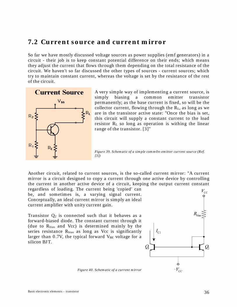
Another circuit, related to current sources, is the so-called current mirror: "A current mirror is a circuit designed to copy a current through one active device by controlling the current in another active device of a circuit, keeping the output current constant regardless of loading. The current being 'copied' can be, and sometimes is, a varying signal current. Conceptually, an ideal current mirror is simply an ideal current amplifier with unity current gain. Transistor Q2 is connected such that it behaves as a forward-biased diode. The constant current through it (due to Rbias and Vcc) is determined mainly by the series resistance Rbias as long as Vcc is significantly larger than 0.7V, the typical forward VBE voltage for a silicon BJT.
Figure 40. Schematic of a current mirror
Basic electronic elements – transistor 36

It is important to have Q2 in the circuit instead of a regular diode because, assuming the two transistors are closely matched, the base current for each transistor should be nearly identical since VBE for each transistor is identical. With nearly identical base currents, the matched transistors should then have nearly identical collector currents as long as VCE2 is not significantly larger than VBE. [36]" Notice that the analysis is based mostly on the Ebers-Moll equations. Of course, one needs to complete the circuit extending above Q1 in order to have current Ic1 flowing. Note also that the figure also shows a -Vcc supply; however this potential can be well set to ground without a problem - as long as the conditions described above are satisfied. It is also advisable to use Falstads circuit simulator applet, to visualise the flow of current in this circuit (there is a built example).
Figure 41. Visualising the flow of current in a PNP current mirror using Falstads applet (Ref. [29])
Basic electronic elements – transistor 37
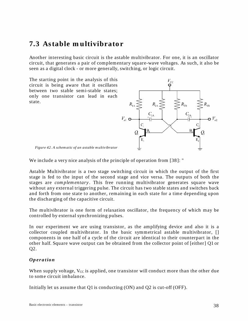
7.3 Astable multivibrator Another interesting basic circuit is the astable multivibrator. For one, it is an oscillator circuit, that generates a pair of complementary square-wave voltages. As such, it also be seen as a digital clock - or more generally, switching, or logic circuit. The starting point in the analysis of this circuit is being aware that it oscillates between two stable semi-stable states; only one transistor can lead in each state.
Figure 42. A schematic of an astable multivibrator
We include a very nice analysis of the principle of operation from [38]: " Astable Multivibrator is a two stage switching circuit in which the output of the first stage is fed to the input of the second stage and vice versa. The outputs of both the stages are complementary. This free running multivibrator generates square wave without any external triggering pulse. The circuit has two stable states and switches back and forth from one state to another, remaining in each state for a time depending upon the discharging of the capacitive circuit. The multivibrator is one form of relaxation oscillator, the frequency of which may be controlled by external synchronizing pulses. In our experiment we are using transistor, as the amplifying device and also it is a collector coupled multivibrator. In the basic symmetrical astable multivibrator, [] components in one half of a cycle of the circuit are identical to their counterpart in the other half. Square wave output can be obtained from the collector point of [either] Q1 or Q2. Operation When supply voltage, VCC is applied, one transistor will conduct more than the other due to some circuit imbalance. Initially let us assume that Q1 is conducting (ON) and Q2 is cut-off (OFF).
Basic electronic elements – transistor 38
Then VC1, the output of Q1 is equal to VCESAT which is approximately zero and VC2 is equal to VCC. At this instant C1 charges exponentially with the time constant R1C1 towards the supply voltage through R1 and correspondingly VB2 also increases exponentially towards VCC. When VB2 crosses the coupling voltage Q2 starts conducting and VC2 falls to VCESAT. Also VB1 falls due to capacitive coupling between collector of Q2 and base of Q1, thereby driving Q1 into OFF state. The rise in voltage VC1 is coupled through C1 to the base of Q2 causing a small overshoot in voltage VB2. Thus Q1 is OFF and Q2 is ON. At this instant the voltage levels are: VB1 is negative, VC1=VCC, VB2=VBESAT and VC2=VCESAT.
When Q1 is OFF and Q2 is ON the voltage VB1 increases exponentially with a time constant R2C2 towards VCC. Therefore Q1 is driven to saturation and Q2 to cut-off. Now the voltage levels are: VB1=VBESAT, VC1=VCESAT, VB2 is negative and VC2=VCC. From the above it is clear that when Q2 is ON the falling voltage VC2 permits the discharging of capacitor C2 which inturn drives Q1 into cut-off. The rising voltage of VC1 is fed back to the base of Q2 tending to turn it ON. This process is regenerative. … Charging and discharging time periods are given by
111 693.0 CRt =
222 693.0 CRt = The total time period T is given by 21 ttT += For symmetrical astable multivibrator: RRR == 21 , CCC == 21 -> RCT 386.1= The free running frequency is given by
RCTf
386.111
== [38]"
Basic electronic elements – transistor 39
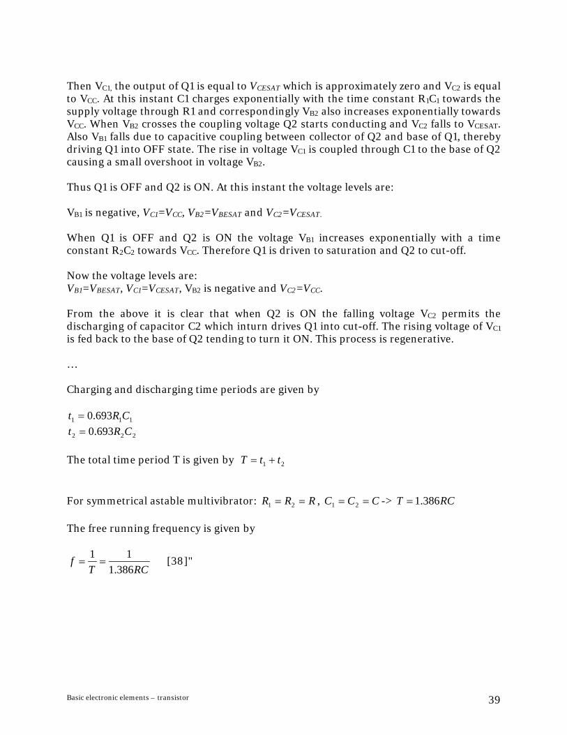
It is also advisable to use Falstads circuit simulator applet, to visualise the flow of current in this circuit (there is a built example).
Figure 43. Visualising the flow of current in an astable multivibrator using Falstads applet (Ref. [29])
Basic electronic elements – transistor 40
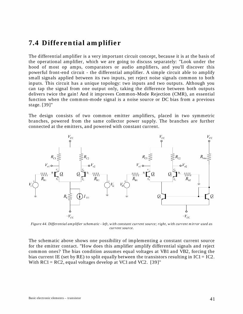
7.4 Differential amplifier The differential amplifier is a very important circuit concept, because it is at the basis of the operational amplifier, which we are going to discuss separately: "Look under the hood of most op amps, comparators or audio amplifiers, and you'll discover this powerful front-end circuit - the differential amplifier. A simple circuit able to amplify small signals applied between its two inputs, yet reject noise signals common to both inputs. This circuit has a unique topology: two inputs and two outputs. Although you can tap the signal from one output only, taking the difference between both outputs delivers twice the gain! And it improves Common-Mode Rejection (CMR), an essential function when the common-mode signal is a noise source or DC bias from a previous stage. [39]" The design consists of two common emitter amplifiers, placed in two symmetric branches, powered from the same collector power supply. The branches are further connected at the emitters, and powered with constant current.
Figure 44. Differential amplifier schematic - left, with constant current source; right, with current mirror used as
current source.
The schematic above shows one possibility of implementing a constant current source for the emitter contact. "How does this amplifier amplify differential signals and reject common ones? The bias condition assumes equal voltages at VB1 and VB2, forcing the bias current IE (set by RE) to split equally between the transistors resulting in IC1 = IC2. With RC1 = RC2, equal voltages develop at VC1 and VC2. [39]"
Basic electronic elements – transistor 41
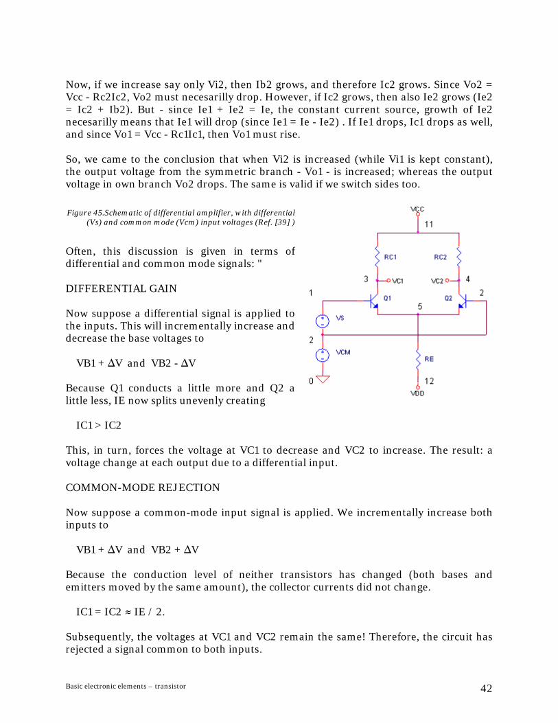
Now, if we increase say only Vi2, then Ib2 grows, and therefore Ic2 grows. Since Vo2 = Vcc - Rc2Ic2, Vo2 must necesarilly drop. However, if Ic2 grows, then also Ie2 grows (Ie2 = Ic2 + Ib2). But - since Ie1 + Ie2 = Ie, the constant current source, growth of Ie2 necesarilly means that Ie1 will drop (since Ie1 = Ie - Ie2) . If Ie1 drops, Ic1 drops as well, and since Vo1 = Vcc - Rc1Ic1, then Vo1 must rise. So, we came to the conclusion that when Vi2 is increased (while Vi1 is kept constant), the output voltage from the symmetric branch - Vo1 - is increased; whereas the output voltage in own branch Vo2 drops. The same is valid if we switch sides too. Figure 45.Schematic of differential amplifier, with differential
(Vs) and common mode (Vcm) input voltages (Ref. [39] )
Often, this discussion is given in terms of differential and common mode signals: " DIFFERENTIAL GAIN Now suppose a differential signal is applied to the inputs. This will incrementally increase and decrease the base voltages to VB1 + ∆V and VB2 - ∆V Because Q1 conducts a little more and Q2 a little less, IE now splits unevenly creating IC1 > IC2 This, in turn, forces the voltage at VC1 to decrease and VC2 to increase. The result: a voltage change at each output due to a differential input. COMMON-MODE REJECTION Now suppose a common-mode input signal is applied. We incrementally increase both inputs to VB1 + ∆V and VB2 + ∆V Because the conduction level of neither transistors has changed (both bases and emitters moved by the same amount), the collector currents did not change. IC1 = IC2 ≈ IE / 2. Subsequently, the voltages at VC1 and VC2 remain the same! Therefore, the circuit has rejected a signal common to both inputs.
Basic electronic elements – transistor 42

Well, the last statement is almost true. Actually, a change in emitter voltage had a small ill effect. It changed the bias current IE set by RE. And this directly impacted IC1 = IC2 ≈ IE / 2, slightly shifting the levels at VC1, VC2. As you can see the rejection is not perfect. However, it can still be effective at removing a large part of noise or a DC bias common to both inputs. [39]" Let us also include the following excerpt: "A differential amplifier is a type of an electronic amplifier that multiplies the difference between two inputs by some constant factor (the differential gain). A differential amplifier is the input stage of operational amplifiers, or op-amps, and emitter coupled logic gates. Note that a differential amplifier is a more general form of amplifier than one with a single input; by grounding one input of a differential amplifier, a single-ended amplifier results. [40]" It is also advisable to use Falstads circuit simulator applet, to visualise the flow of current in this circuit (there is a built example).
Figure 46. Visualising the flow of current in an differential amplifier using Falstads applet (Ref. [29])
Basic electronic elements – transistor 43
8 Sensing application Special implementations of the transistor can also be used as sensor elements. The most typical example is a phototransistor.
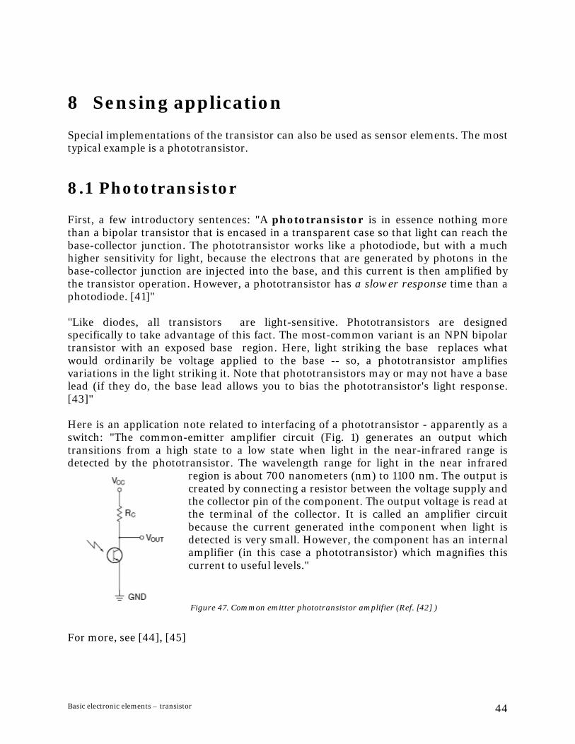
8.1 Phototransistor First, a few introductory sentences: "A phototransistor is in essence nothing more than a bipolar transistor that is encased in a transparent case so that light can reach the base-collector junction. The phototransistor works like a photodiode, but with a much higher sensitivity for light, because the electrons that are generated by photons in the base-collector junction are injected into the base, and this current is then amplified by the transistor operation. However, a phototransistor has a slower response time than a photodiode. [41]" "Like diodes, all transistors are light-sensitive. Phototransistors are designed specifically to take advantage of this fact. The most-common variant is an NPN bipolar transistor with an exposed base region. Here, light striking the base replaces what would ordinarily be voltage applied to the base -- so, a phototransistor amplifies variations in the light striking it. Note that phototransistors may or may not have a base lead (if they do, the base lead allows you to bias the phototransistor's light response. [43]" Here is an application note related to interfacing of a phototransistor - apparently as a switch: "The common-emitter amplifier circuit (Fig. 1) generates an output which transitions from a high state to a low state when light in the near-infrared range is detected by the phototransistor. The wavelength range for light in the near infrared
region is about 700 nanometers (nm) to 1100 nm. The output is created by connecting a resistor between the voltage supply and the collector pin of the component. The output voltage is read at the terminal of the collector. It is called an amplifier circuit because the current generated inthe component when light is detected is very small. However, the component has an internal amplifier (in this case a phototransistor) which magnifies this current to useful levels." Figure 47. Common emitter phototransistor amplifier (Ref. [42] )
For more, see [44], [45]
Basic electronic elements – transistor 44
9 PE Questions • What is the composition of a (bipolar junction) transistor ? • What is the main behavior of a transistor in electric circuits? • Which states do we use to model the behavior of transistor?
Basic electronic elements – transistor 45
Resources and references [1]. Transistor, http://en.wikipedia.org/wiki/Transistor [2]. Bipolar junction transistor, http://en.wikipedia.org/wiki/Bipolar_junction_transistor [3]. Current source, http://hyperphysics.phy-astr.gsu.edu/hbase/electronic/npnce.html#c4 [4]. Testing Transistors with Ohmmeter, http://hyperphysics.phy-astr.gsu.edu/hbase/electronic/trantest.html#c1 [5]. The junction transistor, http://hyperphysics.phy-astr.gsu.edu/hbase/solids/trans.html [6]. habil.dr. Vladimir Gavryushin. “Bipolar Junction Transistors.” Functional combinations in solid states. http://www.mtmi.vu.lt/pfk/funkc_dariniai/transistor/bipolar_transistor.htm [7]. Technolab SA - Techical Education Equipment. “HAKO Section 6 Overhead Models.” Hako - Movable Overheadmodels, Cut-away models. http://www.technolab.org/Hako/Katalog-e/Section6.htm [8]. “Hydraulic analogy - Wikipedia, the free encyclopedia.” http://en.wikipedia.org/wiki/Hydraulic_analogy [9]. SatCure. “How do Transistors Work.” Hobby Electronics Tutorial. http://www.satcure-focus.com/tutor/page4.htm [10]. Dr. Robin N. Strickland. “Course Notes.” ECE 220 Basic Circuits. http://apache.ece.arizona.edu/~ece220/Course_Notes/courseNotes.html [11]. “Transistor models - Wikipedia, the free encyclopedia.” http://en.wikipedia.org/wiki/Transistor_models [12]. “Transistor (Java calculator).” http://www.ee.ucl.ac.uk/~amoss/java/trans.htm [13]. Bill Wilson. “Small Signal Model for Bipolar Transistor.” Connexions . http://cnx.org/content/m11349/latest/ [14]. Andy Collinson. “The Transistor as a Switch.” Circuit Analysis, Design & Theory. http://www.zen22142.zen.co.uk/Design/bjtsw.htm [15]. Tecat: Technical Writing and Educational Consulting. “Visualization Techniques / Understanding Transistors.” http://www.tecat.ca/Visualization.htm [16]. Murat Aşkar. “TABLE OF TRANSISTOR MODELS.” EE 312 Digital Electronics. http://www.eee.metu.edu.tr/~askar/EE312/Transistor_Models.pdf [17]. Dr. Lloyd Bumm. “Lecture Notes on BJT & FET Transitors v1.1.1.” Electronics Lab (Phys2303). http://www.nhn.ou.edu/~bumm/ELAB/Lect_Notes/BJT_FET_transitors_v1_1.html [18]. John Hewes. “Transistor Circuits.” The Electronics Club. http://www.kpsec.freeuk.com/trancirc.htm [19]. Chuck McManis. “Bipolar Junction Transistor Theory.” http://www.mcmanis.com/chuck/Robotics/tutorial/h-bridge/bjt_theory.html [20]. John Hewes. “Multimeters.” The Electronics Club. http://www.kpsec.freeuk.com/multimtr.htm
Basic electronic elements – transistor 46
[21]. Allaboutcircuits.com. “Meter check of a transistor .” Volume III - Semiconductors » BIPOLAR JUNCTION TRANSISTORS . http://www.allaboutcircuits.com/vol_3/chpt_4/3.html [22]. Kilowatt Classroom, LLC. “Introduction to Transistors.” http://web.archive.org/web/20060526125209/http://www.kilowattclassroom.com/Archive/Transistor.pdf [23]. Toy Mayeda, Allan Weber. “Transistor Packages.” EE 459L - Embedded Systems Design Laboratory - Library. http://ee.usc.edu/library/ee459/datasheets/Transistors.pdf [24]. C.R.Wie, SUNY-Buffalo. “BJT-FET Fabrication Applet.” Educational Java Applet Service. http://jas.eng.buffalo.edu/education/fab/BjtFet/index.html [25]. Joe Wolfe . “How do diodes and transistors work?” FAQ in high school physics. http://www.phys.unsw.edu.au/~jw/FAQ.html#diodes [26]. Raymond W.N Chan. “Investigation of the Characteristics of a Transistor (A).” Show One Experiment - Experiment E19. http://www.radian.com.hk/alphyprac/showOneExpt.asp?exptcode=E19 [27]. Bryan Audiffred. “Bipolar Transistor Introduction.” EE 2230 Electronics I - Topics. http://baudiff-2.lsu.edu/~bryan/notebook/S07/EE2230/pages/28.html [28]. Christian Wolff . “npn Transistor Operation.” Radar Basics - Theory of Semiconductors. http://www.radartutorial.eu/21.semiconductors/hl18.en.html [29]. Paul Falstad. “Circuit Simulator Applet.” Math, Physics, and Engineering Applets. http://www.falstad.com/circuit/ [30]. Hyperphysics. “NPN Common Emitter Amplifiers.” http://hyperphysics.phy-astr.gsu.edu/hbase/electronic/npnce.html#c2 [31]. Doug Gingrich . “The Common Emitter Amplifier.” PHYS 395 ELECTRONICS LECTURE NOTES . http://www.phys.ualberta.ca/~gingrich/phys395/notes/node81.html [32]. Chiu-king Ng. “Amplifier (Applet).” http://www.ngsir.netfirms.com/englishhtm/Amplifier.htm [33]. “Common emitter - Wikipedia, the free encyclopedia.” http://en.wikipedia.org/wiki/Common_emitter [34]. Allaboutcircuits.com. “The common-emitter amplifier .” Volume III - Semiconductors » BIPOLAR JUNCTION TRANSISTORS . http://www.allaboutcircuits.com/vol_3/chpt_4/5.html [35]. Innovatia. “Amplifier Circuits.” http://www.innovatia.com/Design_Center/Amplifier_Circuits.htm [36]. “Current mirror - Wikipedia, the free encyclopedia.” http://en.wikipedia.org/wiki/Current_mirror [37]. “IC power supply pin - Wikipedia, the free encyclopedia.” http://en.wikipedia.org/wiki/IC_power_supply_pin [38]. Visionics. “Astable Multivibrator.” http://www.visionics.ee/curriculum/Experiments/Astable/Astable%20Multivibrator1.html [39]. eCircuit Center. “BJT Differential Amplifier.” http://www.ecircuitcenter.com/Circuits/BJT_Diffamp1/BJT_Diffamp1.htm [40]. “Differential amplifier - Wikipedia, the free encyclopedia.” http://en.wikipedia.org/wiki/Differential_amplifier
Basic electronic elements – transistor 47

[41]. “Photodiode - Wikipedia, the free encyclopedia.” http://en.wikipedia.org/wiki/Photodiode [42]. Fairchild Semiconductor Corporation. “Design Fundamentals for Phototransistor Circuits.” Application Note AN-3005. http://www.fairchildsemi.com/an/AN/AN-3005.pdf [43]. Eric Seale. “Phototransistors.” The EncycloBEAMia. http://encyclobeamia.solarbotics.net/articles/phototransistor.html [44]. Radio-Electronics.Com. “Photo transistor (Phototransistor).” http://www.radio-electronics.com/info/data/semicond/phototransistor/photo_transistor.php [45]. PerkinElmer, Inc. “Typical Phototransistor and IRED Applications.” http://optoelectronics.perkinelmer.com/content/ApplicationNotes/APP_IREDAndPhototransistorTypicalApps.pdf [46].
Basic electronic elements – transistor 48


