NASA/TMm2003-211983 Basic Equations for the Modeling of Gallium Nitride (GaN) High Electron Mobility Transistors (HEMTs) Jon C. Freeman Glenn Research Center, Cleveland, Ohio February 2003 https://ntrs.nasa.gov/search.jsp?R=20030014725 2018-05-27T13:07:24+00:00Z
• Telephone the NASA Access Help Desk at301-621-0390
Write to:
NASA Access Help Desk
NASA Center for AeroSpace Information7121 Standard Drive
Hanover, MD 21076
NASA/TM--2003-211983
Basic Equations for the Modeling of Gallium
Nitride (GaN) High Electron Mobility
Transistors (HEMTs)
Jon C. Freeman
Glenn Research Center, Cleveland, Ohio
National Aeronautics and
Space Administration
Glenn Research Center
February 2003
NASA Center for Aerospace Information7121 Standard Drive
Hanover, MD 21076
Available from
National Technical Information Service
5285 Port Royal Road
Springfield, VA 22100
Available electronically at http://gltrs.grc.nasa.gov
Basic Equations for the Modeling of Gallium Nitride (GaN)
High Electron Mobility Transistors (HEMTs)
Jon C. Freeman
National Aeronautics and Space AdministrationGlenn Research Center
Cleveland, Ohio 44135
Summary
Gallium nilride (GaN) is a most promising wide band-gap semiconductor for use in high-power
microwave devices. It has functioned at 320 °C, and higher values are well within theoretical limits. By
combining four devices, 20 W has been developed at X-band. GaN High Electron Mobility Transistors
(HEMTs) are unique in that the two-dimensional electron gas (2DEG) is supported not by intentional
doping, but instead by polarization charge developed at the interface between the bulk GaN regionand the A1GaN epitaxial layer. The polarization charge is composed of two parts: spontaneous and
piezoelectric. This behavior is unlike other semiconductors, and for that reason, no commerciallyavailable modeling software exists. The theme of this document is to develop a self-consistent approach
to developing the pertinent equations to be solved. A Space Act Agreement, "Effects in A1GaN/GaN
HEMT Semiconductors" with Silvaco Data Systems to implement this approach into their existingsoftware for III-V semiconductors, is in place (summer of 2002).
Introduction
This report describes a method to model gallium nitride (GaN) with the Silvaco product ATLAS
and its subroutine BLAZE. Unlike other semiconductor systems, GaN requires the addition of strains
at all parts of the device to include the effects of piezoelectricity. One must also include a spontaneouspolarization at certain interfaces. For these reasons this report consists of 11 sections. Section 1 introduces
notations and definitions, in the area of linear elasticity. Section 2 discusses piezoelectricity and gives the
complete set of basic equations to be solved in a general GaN device. Section 3 introduces spontaneouspolarization. Section 4 indicates the additions needed in the Poisson-Schrodinger solver for GaN analysis.Section 5 gives some critical and basic details on the layer structure ofAIGaN/GaN HEMTs. Section 6
covers band-gap variations, while the remaining sections treat necessary issues to complete the analysis.
Discussion
Our goal is to model A1GaN/GaN HEMTs using Silvaco's existing software platform. For the
A1GaN/GaN system and other III-V nitrides, the effects of both spontaneous and piezoelectric
polarization fields must be included in an analysis. These fields dominate the properties of the 2DEG, and
this report serves as a starting point to incorporate them. The polarizations enter the problem via the
constitutive equation relating D, E, and P :
D=_o_rE +P
NASA/TM--2003-211983 1
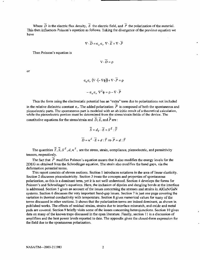
WhereD is the electric flux density, E the electric field, and P the polarization of the material.
This then influences Poisson's equation as follows. Taking the divergence of the previous equation wehave
or
Then Poisson's equation is
V' +V'F
V.D=p
=0
-eoe_ V2_ =p-V.P
Thus the form using the electrostatic potential has an "extra" term due to polarizations not included
in the relative dielectric constant e r. The added polarization P is composed of both the spontaneous and
piezoelectric parts. The spontaneous part is modeled with an ab initio result of a theoretical calculation,while the piezoelectric portion must be determined from the stress/strain fields of the device. The
constitutive equations for the stress/strain and D, E, and P are"
"_=dr .-E +S E :_
--6=, s.2 +a = 7=a :f
The quantities _, S, S E, d, _ s, are the stress, strain, compliance, piezoelectric, and permittivity
tensors, respectively.
The fact that P modifies Poisson's equation means that it also modifies the energy levels for the
2DEG as obtained from the Schrodinger equation. The strain also modifies the band gaps, via thedeformation potential terms.
This report consists of eleven sections. Section 1 introduces notations in the area of linear elasticity.
Section 2 discusses piezoelectricity. Section 3 treats the concepts and properties of spontaneous
polarization, as this is a dominant term, yet it is not well understood. Section 4 develops the forms forPoisson's and Schrodinger's equations. Here, the inclusion of dipoles and dangling bonds at the interface
is addressed. Section 5 gives an account of the issues concerning the stresses and strains in AIGaN/GaN
systems. Section 6 discusses the very important band-gap issues. Section 7 is just one page covering the
variation in thermal conductivity with temperature. Section 8 gives numerical values for many of theterms discussed in other sections. It shows that the polarization terms are indeed dominant, as shown in
published works. The effects of residual strains, strains due to interface mismatch, and oxide and metal
pads are covered. Section 9 briefly visits some of the issues concerning heterojunctions. Section 10 givesdata on many of the known traps discussed in the open literature. Finally, section ! 1 is a discussion of
amplifiers and the best power levels reported to date. The appendix gives the closed-form expression for
the field due to the spontaneous polarization.
NASAfI'M--2003-211983 2
1. Elasticity
This section serves to introduce the needed definitions in elasticity theory that will be utilized later.
Let u = mechanical displacement, then the strain is defined as (ref. 1)
_o. (r,t) = I(OU t O//j]
-2_-_ra+--_r, ) i,j=x,y,z(1)
where Sv means i = direction of displacement (or force)j = normal to surface (face)
Strain is commonly given the symbols e=, U_x,...Now
sxjiSl ss1S= Sxy Syy Sy z A is 6 5 2 -}s4Is= s,__s= L_s_{s4 S 3 J
(2)
Following Auld (ref. 1), Nye (ref. 2), and many others, we use the convention that compressive strain
is negative, while tensile is positive. Note that the factors of ½ and sign convention vary in the literature.Write
S1
$2
_= $3$4
$5
.$6
(3)
The stress is given as
= = T6
rx: ry: r.. r5 r4 r3
(4)
Alternate symbols for Tj are cry,, rw....
NASA/TM--2003-211983 3
Write
rlr2
=r37-4
r5
T6_
Tj < 0 for compression
Ti > 0 for tension
Assume linear theory is applicable, then Hooke's law is valid, so
(5)
TO.= co.laSki (6)
or
S_jkl = So._ Tkl (7)
where Cvklare the stiffness constants (N/m 2) and svkl are the compliance constants (m2/N).
The compact notation is
T = c : S (6a)
S = s : T (7a)
where : stands for the tensor dyadic product. GaN and A1N form in either the Wurtzite (Wz)(hexagonal)
or Zincblende (cubic) crystal classes. For Wz with symmetry notations 6 mm, ca ....
cO =
-Cll C12 C13 0 0 0
C12 ell ¢13 0 0 0
¢13 ¢13 C33 0 0 0
0 0 0 C44 0 0
0 0 0 0 ¢44 0
0 0 0 0 0 Cli --C12
(8)
To summarize
rl
r3
r5
.T6.
¢11
C12
c13
= 0
0
0
¢12 ¢13 0 0 0
ell ¢13 0 0 0
¢13 ¢33 0 0 0
0 0 C44 0 0
0 0 0 ¢44 0
0 0 0 0 Cll -- C12
2
!S1
_$2
$3
$4
$5
_s6J
(9)
NASA/TM--2003-211983 4
$1
S 2
$3
S 4
$5
_$6
SI1 S12 S13 0 0 0
S12 Sll SI3 0 0 0
=/S13 S13 $33 0 0 0
L! 0 0 $44 0 00 0 0 $44 0
0 0 0 0 2(s11 - s12
I
r3
r4rs_r6J
(10)
The determination of the five c,a values is rather difficult. Presently GaN must be grown on a substrate(Sapphire, SiC, ZnO, Si, etc.). The epitaxial growth may be MOCVD, MBE, HVPE, among others; and
the growth rates, gas pressures, and temperatures vary considerably. Under the present situation the filmsvary greatly. They differ in stoichiometry, defects, crystal faults, surface morphology, and film thickness
(nm to lam). For these reasons, among others, one may only expect ranges of values for the fundamental
constants for GaN or A1N. Table I gives two sets of values for the c,a.The first column was derived fromacoustic velocity measurements (ref. 3) on plasma-induced MBE films on Sapphire without a nucleation
layer, with thickness between 800 and 1300 nm. The second column is from best guesses after averagingentries from the literature (refs. 4 to 8).
GaN
Cll
C12
c13
c3_
C44
C66
TABLE I.--STIFFNESS CONSTANTS FOR GaN
c v in GPa
370
145
110
390
9O
112.5
cy (average.
from literature)
382
145
106
389
103
123
IDifference
(percent)[3.2
3.60.26
14
AIN
Cll
C12
C13
¢33
TABLE II.--STIFFNESS CONSTANTS FOR A1N
c,j in GPa
410
140
100
c,/ (average.from literature)
390
125
120
[ Difference
(percent) I4.9
10.7
2O
390 395 1.28
C_ 120 118 1.7
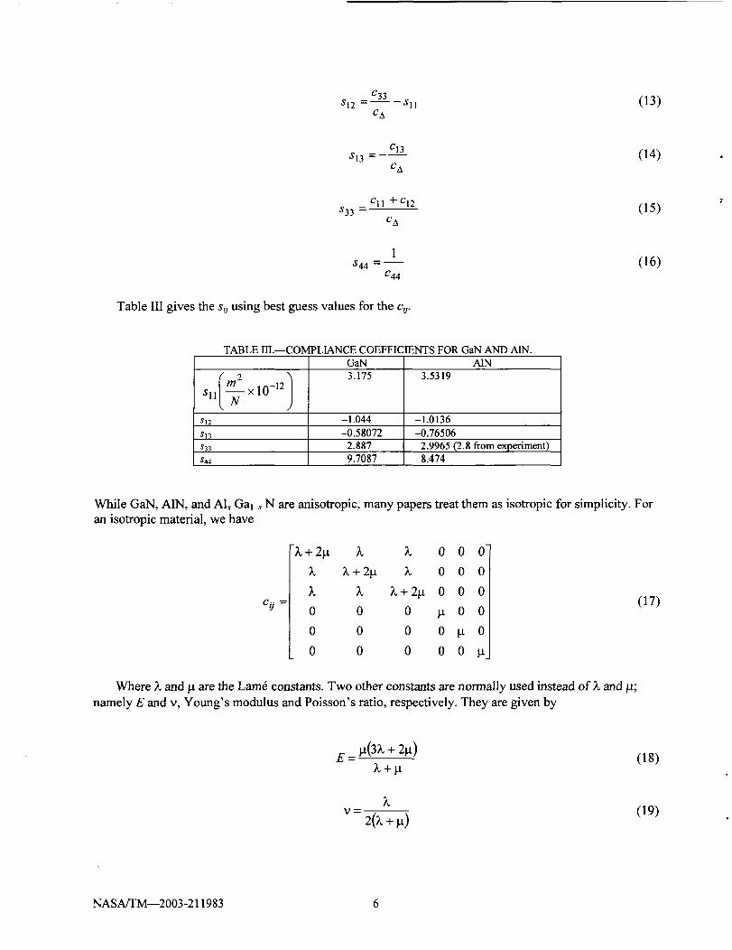
Given the cv the s,j are (ref. 1)
let
CA = C33 (Cll + C12 ) -- 2 c23 (11)
then
,Fc33 1 I (12)
NASA/TM--2003-211983 5
s12 - (13)C33
------SllCA
C13S13 -
C A
(14)
Cll +c12$33 -
c A
1$44 =--
C44
Table III gives the s v using best guess values for the cv.
(15)
(16)
TABLE m.--COMPLIANCE COEFFICIENTS FOR GaN AND A1N.
GaN A1N
2 _ 3.175 3.5319
Sll m x10-12N
s12 -1.044 -1.0136
sl3 -0.58072 -0.76506
$33 2.887
$44 9.7087
2.9965(2.8 _omexperiment)
8.474
While GaN, AIN, and Alx Gal_x N are anisotropic, many papers treat them as isotropic for simplicity. For
an isotropic material, we have
c_ =
r3,+2g 3. 3. 0 0 0-
_. _,+2g _, 0 0 0
_. 2_ ;_+2g 0 0 0
0 0 0 I.t 0 0
0 0 0 0 g 0
0 0 0 0 0
(17)
Where 3. and p are the Lam6 constants. Two other constants are normally used instead of 3. and/.t;
namely E and v, Young's modulus and Poisson's ratio, respectively. They are given by
(18)
(19)
NASA/TM--2003-211983 6
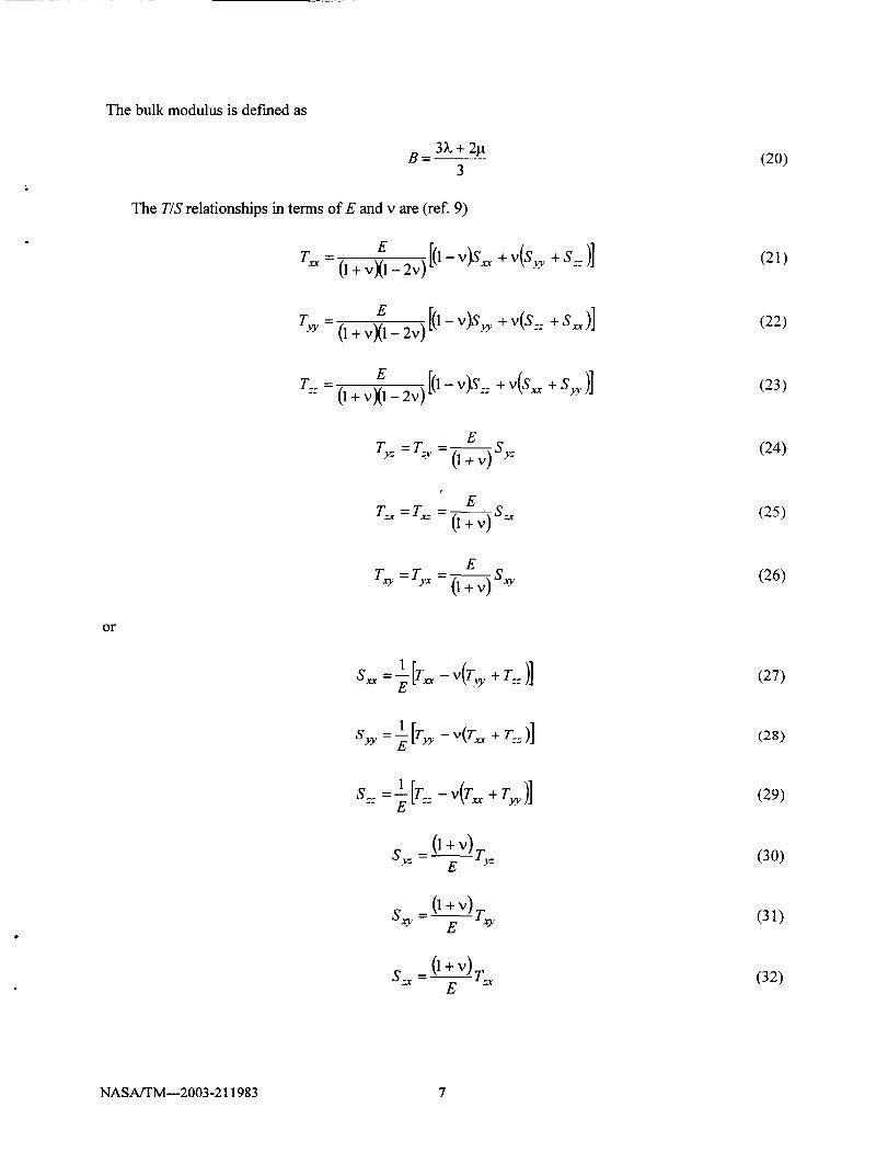
Thebulkmodulusis defined as
3_, + 2_tB-
3
The T/S relationships in terms of E and v are (ref. 9)
E
r==0+,,)0- 20[0-,,)Sx_+_(s.¢+s::)]
E [0-,,)S_y+,,(s::+s_)]Tyy = (1 + vX1 - 2v)
E
T:: - (1 + vX1 - 2v)[(1 - v)s= + v(S_ + Syy )]
E
Ty: = T. v =-_ Sy:.
E
T:_ =Tx: =-o-_S:x
E
ray = Tyx =-_--_ Sxy
(20)
(21)
(22)
(23)
(24)
(25)
(26)
or
1 T ._
1_ =_ [,-_y-,#= +_:)]
(27)
(28)
1
s,_- (l_)r_.
s_ -_7;_(1+v)_
(29)
(30)
(31)
(32)
NASA/TM--2003-211983 7
There are several special cases:
Plane strain (6'.-:= 0)
or
E
r= 0+vXl-2v):,_ ,. [(,__ +%]
_ g
T - Ev
E
(33)
(34)
(35)
(36)
(37)
Plane stress (T= = 0)
S..=O
Sy: =S_: =0
08)
(39)
(40)
(41)
(42)
NASAFFM_2003.211983
E
E
T:_--0
E
8
(43)
(44)
(45)
(46)
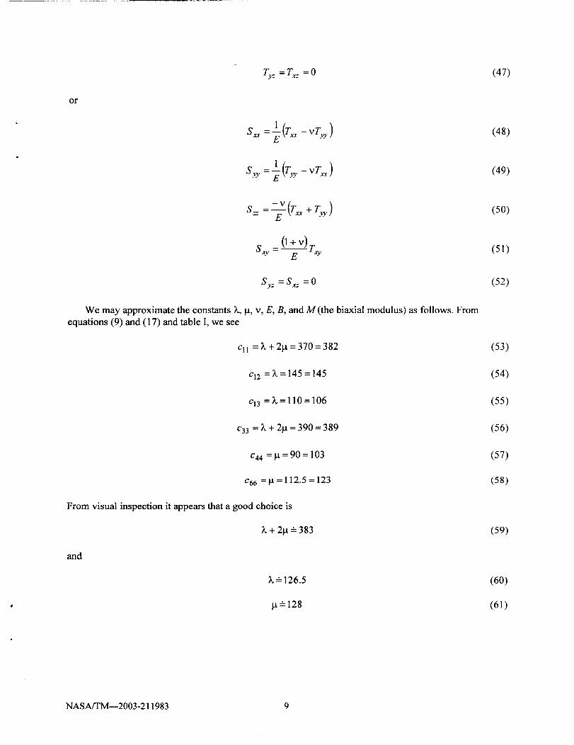
Ty. = Tx_ = 0 (47)
or
1 Tsxx=7(xx-v ,)
1 T VTxx)S,y =_-( _,-
= +T._
(48)
(49)
(5O)
sx,,- (1Ev)Y y
Sy: = Sx: = 0 (52)
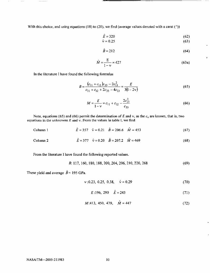
We may approximate the constants _, _t, v, E, B, and M (the biaxial modulus) as follows. Fromequations (9) and (17) and table I, we see
Cll = _. + 2p = 370 = 382 (53)
c12 = _. = 145 = 145 (54)
c13 = _. = 110 = 106 (55)
¢33 = _"+ 2_t = 390 = 389 (56)
C44 = }.1,= 90 = 103 (57)
c66 = }J. = 112.5 = 123 (58)
From visual inspection it appears that a good choice is
In the literature I have found the following formulas
B= (¢11 +c12)c33 - 2c23 _ E
Cll + c12 + 2c33 - 4c13 3(1 - 2v)(65)
E 2c23M- -ell +c12 ---
1 - v c33(66)
Note, equations (65) and (66) permit the determination of E and v, as the cu are known, that is, twoequations in the unknowns E and v. From the values in table I, we find
Columnl J_=357 _=0.21 /_=206.6 )V/=453 (67)
Column2 E=377 (,=0.20 /_=207.2 /Q=469 (68)
From the literature I have found the following reported values.
This demonstrates the uncertainty in the magnitudes of the quantities in this section.
Estimation of Stress and Strain
We assume the stress in the layers may be conceptually described by the superposition of three
components:
_TOTAL = OEXTERNAL + _THERMAL + GINTRINSIC
The thermal part is the most straightforward, it is
OTHERMA L = OTH = ActAT--E
1-v
(81)
(82)
NASA/TM--2003-211983 12
Where Aot is the difference in thermal expansion coefficients (TEC), between the layers. Also AT is
the difference between the growth temperature and the sample temperature (generally room temperature
(RT)). The above assumes the substrate and epilayer are relaxed at the growth temperature (not true ingeneral), and that no relaxation during cooling has taken place.
The external portion (aEXV) is due to loading by adjacent layers; lattice mismatch, metal pads, andany recognizable force. The last term is referred to as intrinsic or residual stress; it acts as a catch-all for
stresses that do not fit into the two previous categories. The residual stresses are difficult to handle
because they depend on growth parameters, which differ greatly for the basic growth methods. The basicmethods are MBE, MOCVD, HVPE, and variations of them. Some of the parameters are growth
temperature, pressure, gas flow rates, substrate crystal orientation, surface conditions, and preparation
procedure. The GaN is often grown on a nucleation layer of either GaN or AIN. The properties of thenucleation layer include thickness, growth temperature, and doping. Finally, defects produced by
vacancies, cracks, misfit dislocations, threading dislocations, etc.
After the stress has been quantified the strain will still not be known exactly, as the material responds
to stress in at least two ways. One is to strain via Hooke's law, the other is to generate defects andpropagate them throughout the material (relaxation). Finally, cracks do occur in GaN and sapphire, and
many in the GaN are not visible by observation of the surface.
External Stress/Strain
Most often the strain due to lattice mismatch is assumed to be the dominant factor. Def'me the misfit
parameter
fm- a - a o (83)a0
where a0 is the relaxed lattice parameter and a is the strained value. The strain is then
_xx=+ fm (84)
where the appropriate sign is chosen. Maeda (ref. 11) introduced a "lattice relaxation ratio, R" by
0 R) (85)E X,lt. _ -- __
a0
This is very useful, as it permits some relaxation at the interfaces. The corresponding stresses are
E Ac Ea m .... _.. (86)
2v co 2v "
E Aac_ - = M exx (87)
1-v a 0
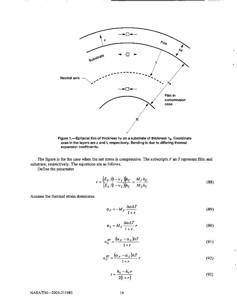
where Ac/co is the strain along the c-axis, and Aa/ao is that in the basal plane. The composite stress in agiven film, or layers of film may be calculated at several levels of approximation. We start with Etzkorn
(ref. 12).
NASA/TM--2003-211983 13
R
/Figure 1.--Epitaxial film of thickness hF on a substrate of thickness hs. Coordinate
axes in the layers are z and t, respectively. Bending is due to differing thermalexpansion coefficients.
The figure is for the case when the net stress is compressive. The subscripts F an S represent film and
substrate, respectively. The equations are as follows.
Def'me the parameter
r= [Es/O_Vs)]hs- Mshs (88)
Assume the thermal strain dominates
ActAT(_F = -ME -- (89)
l+r
ActATo s = M s -- r (90)
l+r
e_v= (ct F -ct s )aT (91)l+r
eRSr- (a F -a s )AT r (92)l+r
t = hs - hFr2(1 +r) (93)
NASA/TM--2003 -211983 14
AaAT 6(h s - 2t) _ 6(h F + 2t) + (hs + hF (94)
z+t_EF (Z) =_RT nt (95)
R
Notice equation (95) gives the strain as a linear function of distance z from the interface. Equation
(94) gives the radius of curvature. Observe that this formulation only requires material parameters and thethickness of the substrate and film.
Next, the equation of Skromme (ref. 13):
Msh +MFh - 3MFh (hs+CSURFACE = 6(hs + h F )hF R
(96)
where R is the radius of curvature which must be measured. Kozawa (ref. 14) has a slightly simpler form
(assumes v the same in both layers)
Esh3s + EFh3F
c Y = 6(1 -- vXh s + h y )h y R(97)
TABLE V.--DATA FROM REF. 14 WITH OTHER
ENTRIES IN PARENTHESES
E (GPa)_c Oo-_)v
Sapphire300
425
GaN
2.5 to 48.8
196(295)5.457.5
0.3 (0.25) 0.3 (0.25)
From Hearne (ref. 15) we have Stoney's formula:
Msh2s(YF--
6hER
where for MOCVD at 1050 °C; sapphire: M = 450 or 479, depending on wafer; 6H-SiC: M = 586 GPa.Then
I_F -= axx = MF _xx
The composite stress was measured to be tensile with range
0.14 < 6_ < 0.29 GPa
(98)
(99)
NASA/TM--2003-211983 15
Thethermalcomponent(bymeasurements)was-0.66+ 1 GPa, and the theoretical thermal
component is -1.4 + 0.7 GPa. Thus, the residual and perhaps some lattice portion dominates the stress
in the given films. The radius of curvature R is determined by surface profilometry or laser reflection.
Generally
2m<R<20m
and in most cases R < 6 m. However, R = 0.58 m for HVPE films.
Some experimental data (though incomplete) is helpful. From reference 16 a sample consisting of
a 6H-SiC substrate with 3p of porous GaN, then 3_t of HVPE GaN on top. The surface was in tension(wafer like a cup that holds water). The radius of curvature R was -6.5 m, the in-plane stress was0.64 GPa, and the strain along the c-axis was -1.12 x 10 -3. The substrate thickness was not given.
A common range of parameters for GaN on sapphire is: 250 btm of sapphire with 500 A of AIN
nucleation layer, and 1 to 5 lam of GaN. The residual strain in the GaN is of the order of 1.0 × 10⁻⁴.
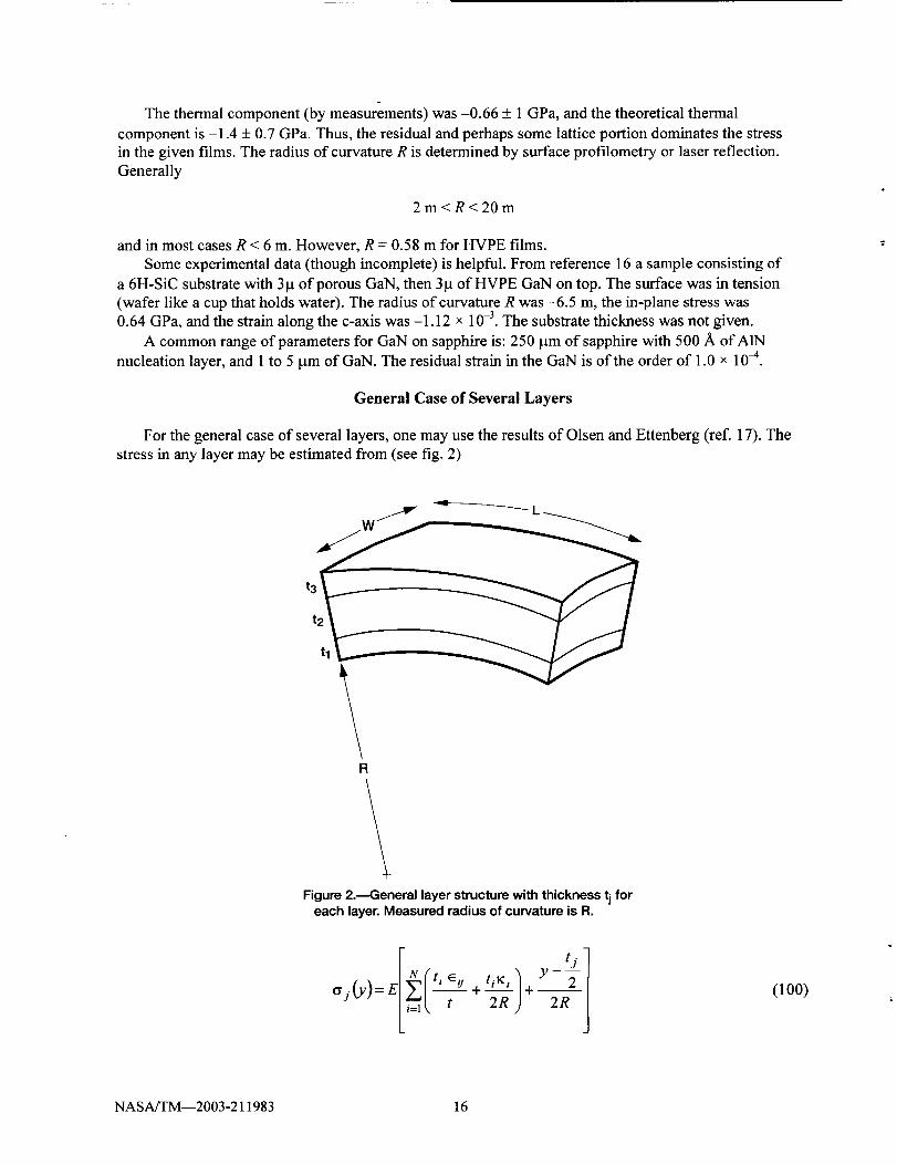
General Case of Several Layers
For the general case of several layers, one may use the results of Olsen and Ettenberg (ref. 17). Thestress in any layer may be estimated from (see fig. 2)
t2
tl
1R
Figure 2.---General layer structure with thickness tj foreach layer. Measured radiusof curvature is R.
+m2R
(100)
NASA/TM--2003-211983 16
Hereit isassumedthattheelasticmoduli(Young'smoduli)ofall layersarethesameandequalto E. Inequation (100)y is measured from the bottom ofthej th layer. The terms in equation (100) are
N
t=_t i
t=l
(lOl)
( /-IN N
R=t 3 6_ _'tit J _gk i=1 j>l
(]02)
_:, =1 i<j
_ci =0 i=j
_:i =-1 i>j
(103)
In equation (102) the strain at the interface of the ithandj th layer _v is related to the measured radius
of curvature. However, it is assumed the strains e 0 are known, along with the thickness t, of each layer.Ifw-L, then one may assume spherical bending, then a two-dimensional (2D) solution may be obtained
from the given one-dimensional (1D) by
(Y)ID_j/ \
°i lY)2D - (104)l-v
Reasonable choices for the interface strains are the larger of thermal, lattice mismatch, or residualstrains (ref. 18). The reviews in references 19 to 22 should be consulted for more information.
2. Piezoelectricity
This section details equations we will use later. It is important to note that this discussion treats
dielectrics, not semiconductors, that is, effects of cartier screening are ignored. We start with the defining
equation for D, E, and P.
Here
D=e 0 E+P (105)
B
P = PELECTRONIC + PIONIC + POTHER (106)
In most cases only the first two terms in equation (106) are assumed to exist, and POTHER is assumed
equal to zero. This case then has the constitutive assumption that the polarization is linearly related to the
E field,
PELECTRONIC + PIONIC_ C 0 _e _ (107)
NASA/TM--2003-211983 17
where)_eis the polarizability. Then
D=E 0 E+E 0 Ze _
=EOE r g (P-oTHER ____O)
which is the normal case. For anisotropic material we write
1 D = Kyx K_ Ky:
K zx Kzy K zz
We use K since c is used so often for strain. Thus
1--D=_c.ECO
(108)
(109)
(11o)
or
1
C o
-- Oj = KijE j i, j = x,y,z
for GaN and A1N, we have (ref. 20)
KI1 0 0 10 r:11 00 K33
(111)
for GaN, KI_ = 9.5 and _¢33= 10.4
for AIN, Kll ---- 9.0 and K33 ---- 10.7
Now when the dielectric material is also piezoelectric (following Auld, (ref. 1))
(112)
which are the piezoelectric strain equations. Another form is
T=-e:E+c E :S
D=c o Ks .E+e:S(113)
which are the corresponding stress equations. The superscripts mean constant electric field E, constant
stress T, or constant strain S. By inspection we observe (now ffOTI-mR = ffPlZZOELECTmC)
P=d:7 _ (114)
NASA/TM--2003-211983 18
where d,j are the piezoelectric strain constants. We also have
P=e;S
where e v are the stress constants. For our Wz crystals we have (refs. 1 and 23)
Py = 0 0 d15 0
P.. d31 d31 d33 0 0r4r5
56J
(115)
(116)
with the associations T1 = 01 = on, Tz = 02 = Oyy, T3 = 03 = 0=, T4 = o4 = 0., T5 = o5 = ox.-, T6 = (_6 = (_xy
As in section 1, the range of the coefficients is large.
The following strain constants are in units of 10 -l° cm/V (see refs. 22 to 26):
d3_
d_
dis
TABLE VI.--PIEZOELECTRIC STRAIN CONSTANTS OF GaN
Measured
-0.9Calculated
-1.16
Estimated
-1.7
Bulk
-1.9
Clamped
-1.4
Polycrystal
-1.0
2.39 3.7 2.8 2.0
-3.1 -2.75
The following strain constants are in units of 10 -1° cm/V:
d31
d33
dis
TABLE VII.--PIEZOELECTRIC STRAIN CONSTANTS OF A1N
Measured
-2.05.0
Calculated
-2.65
5.53
-3.4
Estimated-2.71
6.72
Bulk
-2.8
5.6
Clamped
-2.0
4.0 (3.2 film)
Polycrystal
-2.71
-3.6
Theory says d31 = -(1/2) d33. The alternate representation is
P=e:S
or
000e15!]Py = 0 0 el5 0
P: e31 e31 e33 0 0
f.u¢
tyy
ty=
tzx
_xy.
(117)
NASA/TM--2003-211983 19
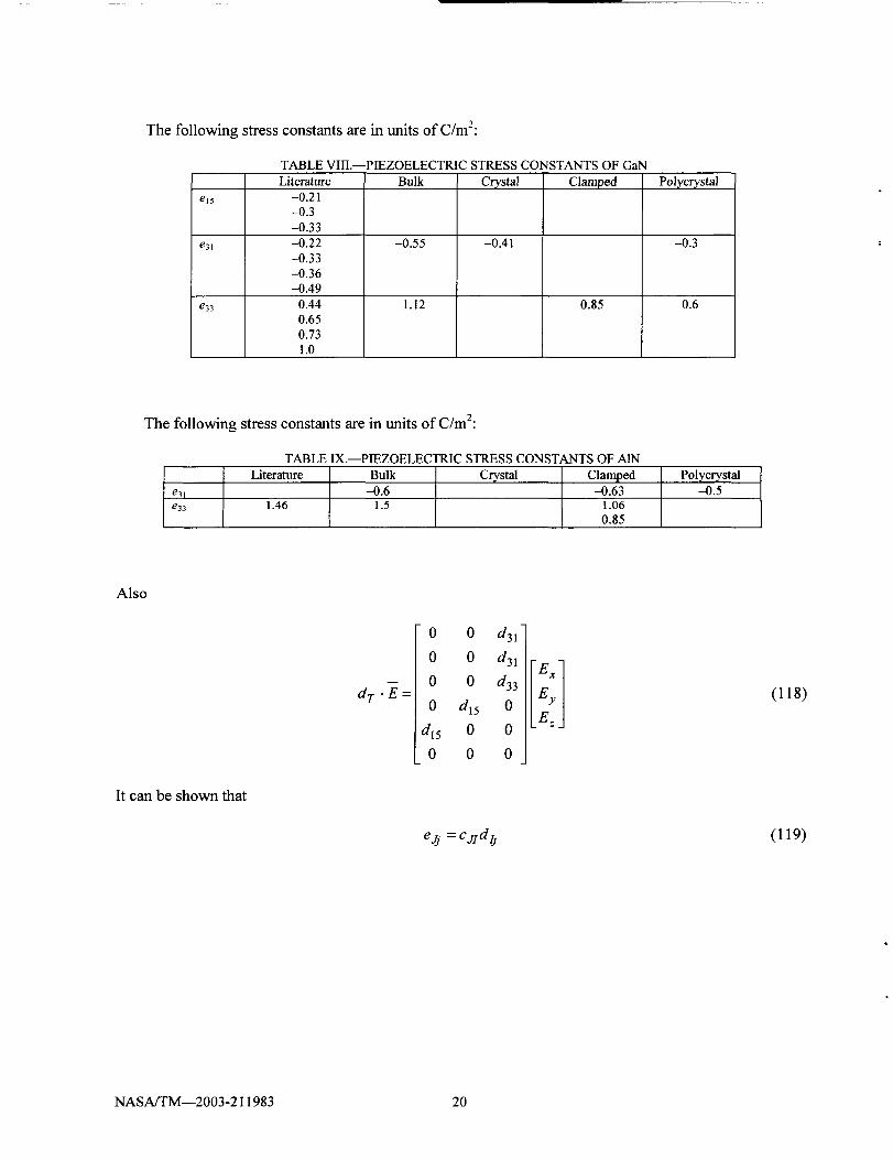
Thefollowingstressconstantsareinunitsof C/m2:
TABLEVIII.--PIEZOELECTRICSTRESSCONSTANTSOFGaN
el5
e31
e33
Literature-0.21-0.3-0.33-0.22-0.33-O.36-0.49
0.440.650.731.0
Bulk
-0.55
1.12
Crystal
-0.41
Clamped
0.85
Polycrystal
-0.3
0.6
The following stress constants are in units of C/m2:
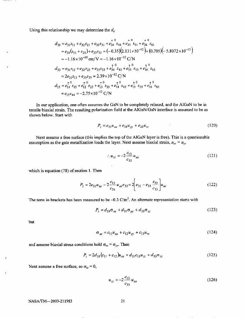
to 1, o _o ?o 1,o tod15 =ell s15 +el2 $25 +el3 $35 +el4 s45 +el5 s55 +el6 $65
= e15s44 = -2.75 × 10⁻¹² C/N
In our application, one often assumes the GaN to be completely relaxed, and the AIGaN to be intensile biaxial strain. The resulting polarization field at the AIGaN/GaN interface is assumed to be asshown below. Start with
P. = e31Uxx + e31Uyy + e33uz: (120)
Next assume a free surface (this implies the top of the A1GaN layer is free). This is a questionable
assumption as the gate metallization loads the layer. Next assume biaxial strain, Ux_= Uyy
The corresponding electric field is (assuming D = 0, which means no charge is present)
E. P" 2d31 I c2 ]13 (129)-- -- ell + C12 ---- Uxx
E0E r E0E r C33 .J
This field is about 6x10⁶ V/cm. equations 128 and 129 are found in the literature, (refs. 5, 27, and 28),
and many have a factor of two before the c_3/c33 term. I interpret them as errors by attempting to add
u_ and u_ together as the "net strain" in the basal plane. For our case ofAlx Gal_xN, some authorsmultiply the P= in equation (128) by the mole fraction x to obtain the effective value.
With the preceding concepts in place, we may introduce the entire set of equations to be solved in theGaN/A1GaN system. The first group consists of the mechanical equations of equilibrium (ref. 29)
OTyx OT._
_x + Oy + Oz -qn-_x=0
OTxy + _t_yy + t_]"=y _qn_d_ =OOx Oy Oz
OTx=OT,,xOx + --_-- + --0_-z"- q" -0--zz=0
(130)
The last term in each equation is the "body force," which we assume is the charge density times the
electric field. Next, the electromechanical constitutive equations are
(Yxx
(Yyy
r.x
Cll
C12
C13
= 0
0
0
C12 C13 0 0 0
ell C13 0 0 0
C13 C33 0 0 0
0 0 C44 0 0
0 0 0 C44 0
0 0 0 0 C11 - C12
2
Exx
Eyy
Yy=
_Y_yJ
0 0 e31 -
0 0 e31
0 0 e33
0 e15 0
e15 0 0
0 0 0
I ]Ey
E:
(131)
NASA/TM--2003-211983 22
[ox][Ka0 000Dy =E 0 0 Kll 0 E v + 0 0 el5
D: 0 0 K33 E_ e31 e31 e33 0
1Exx
0 0Ezz
o _'y:J0
_Yxy
Ou 8v 8w=_-xx, =_-y),, E
8x 8z ""
8v 8w 8u Ow 8u o%,
-- + -- = Y v:" -- + -- = Y:X"SzOy " Oz Ox -_ Ox+-- = YxY
which couple the stress, strain, electric field, and electric displacement. The latter expressions are the
compatibility expressions (ref. 29) relating strains to the material displacements. Notice the notation formechanical displacements uses u, v and w; rather than just u with a subscript. The last expressions to be
used are the continuity, Gauss, and current equations.
a, aj_+aJ_ aJ.+---= = 0EX _--m
G - a, J_=_,x.(_)Ex+D. a.(___))oy ax
On(_ )E. =_L* Jy = g:(_)ey + D.
" az ay
J. =....(_)E:+z_.o.(_)" 8z
(132)
(133)
(134)
019x + ODy 019.+ -----_"= qn(_) (135)Ox oy az
_ e-
n = n(_)= n(x, y, z ) _mm3 (136)
where we have assumed just electrons are present. Similar terms for holes may be added for the most
general case. Notice, we have 20 equations in 20 unknowns. This is an extension of the general elasticityproblem to include a piezoelectric semiconductor. In elasticity theory, one has 15 equations in15 unknowns.
The total set of equations has been provided for the sake of completeness. In principle they wouldbe solved along with Poisson's and Schrodinger's equations in the Poisson-Schrodinger solver which
presently exists in the software package.
NASA/TM--2003-211983 23
3. Spontaneous Polarization
There is some uncertainty about spontaneous polarization, PSPON, (see refs. 30 to 41). Bernardini
et al., have performed ab initio calculations for spontaneous polarization in nitrides (refs. 30 to 34).Reference 34 discusses some of the controversial issues on the subject. On page 912 of (ref. 37)we quote
"The latter distortion--henceforth called internal strain--determines a preferred polarity of the tetragonal
axis and is responsible for the occurrence of spontaneous polarization." I interpret the discussion to meanthat there is an alteration of the position of atoms in a cell, which is deemed an internal strain (not
apparent macroscopically), which causes the spontaneous polarization. From reference 38, "The so-called
pyroelectric fields then arise from the temperature dependence of the spontaneous polarization when the
temperature is changed." Figure 1 in reference 39 shows both a macroscopic strain _ and an internal
strain u. Apparently u may exist when _ = 0, so a polarization may exist due solely to u; which would be
a (macroscopically) strain-free polarization (spontaneous). A procedure to measure PSPON is given inreference 41.
PsPoN is screened by charges adsorbed onto the surfaces of the material, as well as being screened
by free charge in the bulk. It is assumed (or defined) to be either uniform or zero in the bulk. One paper,
not referenced here, stated it was zero in the bulk. Its presence is known only at interfaces with other
materials (air being one of them). Pyroelectricity is the production of an electric field between twosurfaces of the material held at different temperatures.
PI'VRO = P A Temperature (137)
=(Px_x +pyay + (138)
For GaN
Px = Py = 104 V basal planem.K
p: = 7 x 10⁵ V along the c-axism.K
F
Both Wz AlxGal_xN and GaN possess PsPoN, and at their interface a positive bound surface charge exists
(cubic GaN is piezoelectric but does not possess spontaneous polarization). This assumes a Ga face (onlycase we consider). This immobile charge is assumed (calculated) to reside in a layer 3 to 4 ,_ thick, (I will
draw it in the AIxGal__N region for clarity). Figure 3 depicts two ideal samples with their bound
polarization charges (no screening).
NASA/TM--2003-211983 24
I AINPSPON
i (0001)C-axis
+ + + + + + + +
PSPON(AIN)= -8)<10 .2 C/m2az I PSPONGaN
÷ ÷ ÷
PSPON(GaN)= _2.9×10-2 C/m2 az
Figure 3•mldeal samples of AIN and GaN illustratingspontaneouspolarizations.
Note the z-axis and the c-axis are collinear. This relationship was assumed by Bernardini et al., and is
important with respect to algebraic signs. Recall that the polarization vector P is defined to originate onnegative bound charge and terminate on positive bound charge. The materials are assumed to grow from
the bottom and increase in thickness as one moves up the c-axis (0001). From a simple charge super-
position argument, a net positive bound charge density a(SURF) exists at the surface• Analytically, we
have
t_SLrRF = (8- 2•9)x 10-2 C/m 2 = 5•1 x 10⁻² C/m 2
= 3.19 x 10¹³ e/cm 2(139)
Recall that at a boundary (see fig. 4)
Pn2 - Pnl =-o( su#ac_•Bound
@
Figure4.--Definition for bound surfacecharge atinterface between two polarized dielectrics.Here P2 "-_= Pn2....
For our case
Pn2 = _ •n=(-8xl0-2a:)•a- - =-8x10⁻² C/m2
Pr_ = fill"n=(- 2•9× 10⁻²a:)•a= =-2.9x 10⁻² C/m2
• Pn2 -Pr_ = -8x10⁻² + 2-9x10-2 = -5"1×10⁻² C/m2
• -5.1 × 10⁻² C/m2 _,_(SUR_ACE)= _"BOUND
• 9_o_CE)_c(SURF)= 5.1× 10 -2 C/m 2
(140)
NASA/TM--2003-211983 25
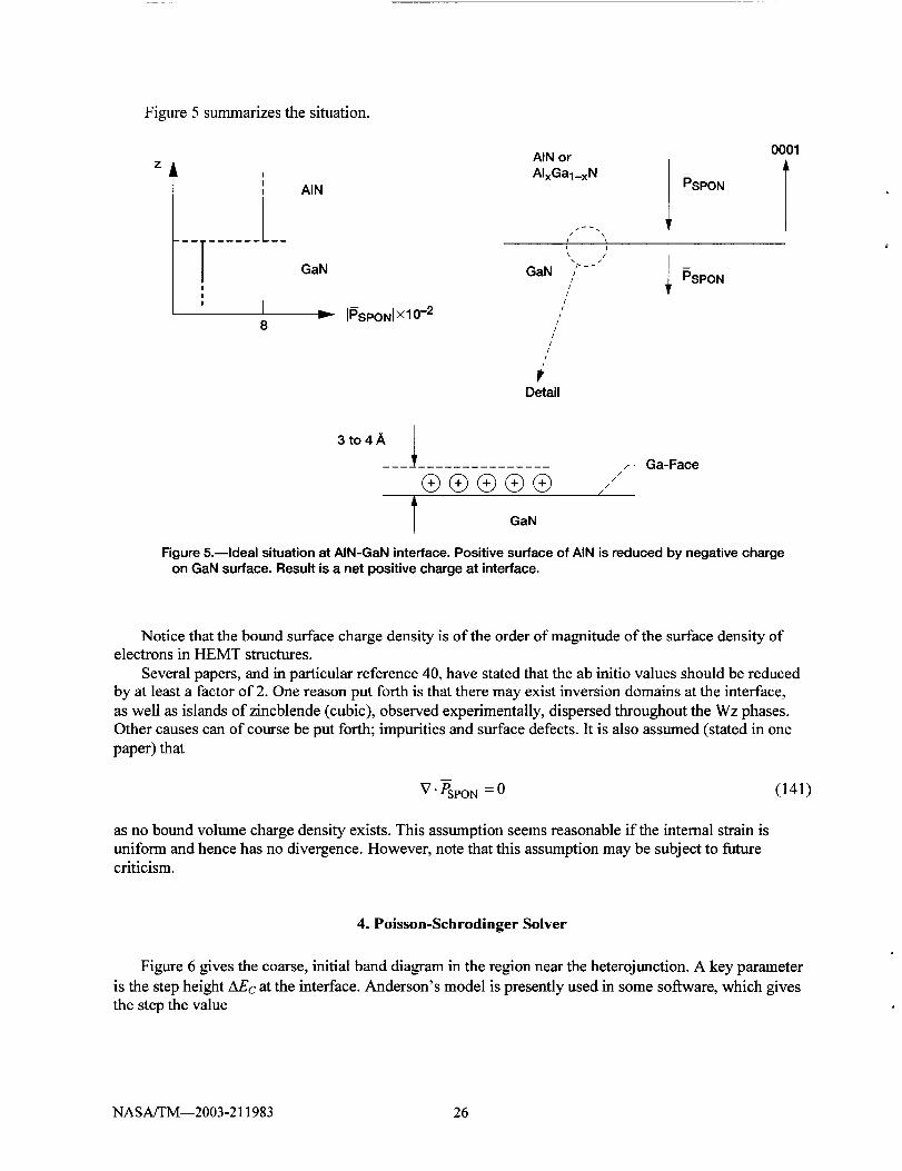
Figure 5 summarizes the situation.
I
I
, AIN
--[ ...... [-- GaN
I
" I8
_ I#SPONIXIO-2
AIN orAIxGal_x N
GaN
PSPON
I f
\
\ // t
!
/
/t
i I
I/
i/
//
/
iDetail
PSPON
0001
T
3to4A.... r Ga-Face
l GaN
Figure 5.--Ideal situation at AIN-GaN interface. Positive surface of AIN is reduced by negative charge
on GaN surface, Result is a net positivecharge at interface,
Notice that the bound surface charge density is of the order of magnitude of the surface density ofelectrons in HEMT structures.
Several papers, and in particular reference 40, have stated that the ab initio values should be reduced
by at least a factor of 2. One reason put forth is that there may exist inversion domains at the interface,
as well as islands of zincblende (cubic), observed experimentally, dispersed throughout the Wz phases.Other causes can of course be put forth; impurities and surface defects. It is also assumed (stated in one
paper) that
V "PsPoN = 0 (141)
as no bound volume charge density exists. This assumption seems reasonable if the internal strain is
uniform and hence has no divergence. However, note that this assumption may be subject to futurecriticism.
4. Poisson-Sehrodinger Solver
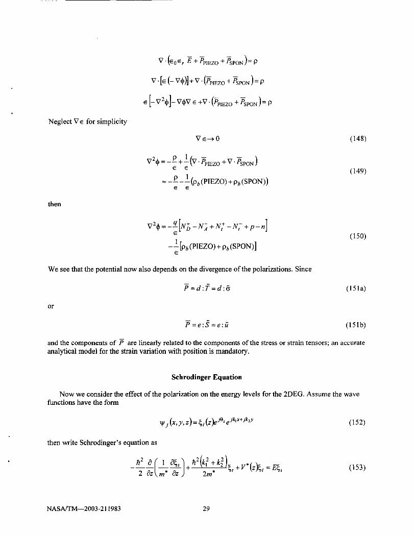
Figure 6 gives the coarse, initial band diagram in the region near the heterojunction. A key parameter
is the step height AEc at the interface. Anderson's model is presently used in some sottware, which gives
the step the value
NASA/TM--2003-211983 26
AIxGal_x N GaN
Z
E C
Figure 6.mldeal triangular well for confinement of 2DEG at interface
of AIxGa l_x N and GaN layers. Conduction band edges are denoted
as E c.
AEc = _ AlxGa__xN --_,GaN (142)
where ;( is the electron aff'mity. We will discuss alternative ways to estimate AEc in later sections. Thetriangular well is composed of the step and the sloping side. The linear variation means a constant electric
field is present. Apparently the establishment of the field comes about as follows. At the heterojunction,
the step in Ec along with the position of the Fermi level causes electrons to accumulate in the notch. The
region into the bulk on the left is therefore depleted, and the existing donors establish the field. The fieldis modeled by the standard depletion approximation
E(o):q [ND :'qNs ] (143)
where
No = depletion region sheet density
Ns = free carrier sheet density
11 = a weighting factor (-0.5 to 0.8)
GaAs value at the heterojunction is
E(0)= 2.39 x 10⁶ V/m (144)
For our case of AlxGal_xN/GaN, the situation is apparently quite different. From Sacconi (ref. 42), if
we initially neglect all polarization, then the step height and Fermi levels (for typical doping) are not
sufficient for a notch to form. Then electrons do not accumulate and create the 2DEG. After adding the
spontaneous and piezoelectric factors, the notch forms, and the 2DEG is present. Apparently a depletionregion does not form, as the polarization charge is sufficient to establish the field. If one does form,
perhaps it is swamped by the polarization charge. One may look at the situation as follows: the 2DEG
NASAfI'M---2003-211983 27
forms to screen the bound spontaneous and piezoelectric charge residing at the interface. This introduces
the question, "where do the electrons come from that establish the 2DEG?" There are valid reasons that
state they cannot come from the bulk GuN, so apparently they come from donors somewhere in theAlxGaI__,N region. This is not a trivial issue, as charge neutrality must hold, but the bookkeeping is not
generally agreed upon in the literature. Instead of using the field expression developed from the depletionapproximation, authors assume it should be represented by equation (129) in section 2,
[ 2]E. 2d31 c13-- Cll +C12 ---- U_r
E 0 E r C33
(145)
If the strain in the AlxGal__N is tensile Uxx> 0, then the field is oriented toward the bulk just as in the
case of the depletion approximation. Figure 7 summarizes the discussion.
AIGaAs
Donors --_r -X .....
I I
I i
I---I_-- 2DEG
(a)
Depletionmodel
AIxGal_x N
Polarization r_
charge _ _ J+lII
(b)
Figure 7.m2DEG formation. (a) By intentional doping. (b) By polarization charge.
Poissou's Equation
Without spontaneous or piezoelectric polarization, Poisson's equation is
vErb= P- q[N/_-N]+N +-N t-+p-n]E E
(146)
+ - + Nt-- are ionized donor/acceptor densities, and ionized donor/acceptor trap densities,where No, N A , N _ ,
respectively. Also
E=EOE r(147)
q=lel= +l.6×lO-19C
The relative dielectric constant _ r considers the standard electronic plus ionic polarizabilities. When
both spontaneous and piezoelectric polarizations are included, the form is as follows.Start with
V-D =p
v.( o
NASA/TM--2003-211983 28
NeglectV e for simplicity
then
v (e0_,E+p_._,o+_o_)=
V "[E (-- V(_)]+ V" (PPIEZO + PSPON )= [3
V _--_ 0
v__=--_+l(v._zo+v.Go_)E E
= __P_ ! (Pb (PIEZO) + Pb (SPON))E
q + +p-n]V2dp=--_[ND-N] + Nt-N t
1 [Pb(I'IEZO) + Pb(SPON)]E
We see that the potential now also depends on the divergence of the polarizations. Since
-P=d:T =d:6
(148)
(149)
(150)
(151a)
or
ff=e:S =e:ff (151b)
and the components of P are linearly related to the components of the stress or strain tensors; an accurateanalytical model for the strain variation with position is mandatory.
Sehrodinger Equation
Now we consider the effect of the polarization on the energy levels for the 2DEG. Assume the wavefunctions have the form
V j(x,Y,Z)=¢i(g) ejOzejk'x+jk2y
then write Schrodinger's equation as
h22 Oza( lm, O_')Oz+h2(k}+k2)2m* _,+V*(z)_ i=E_,
(152)
(153)
NASA/TM--2003-211983 29
Weusean asterisk on the potential energy (PE) term V*(z), to denote that it represents the total potential
energy field that establishes the well. The potential energy near the well is given in figure 8. The figure
needs to be discussed in some detail. First, recall the relationships between the electric field E(z), the
electrostatic potential dp(z) and the electron potential energy band diagram (ref. 43)
Ec(AIxGal-xN) __
Ec(GaN)
I
I
Figure 8.--First-order approximationof potential energy well at heterojunction.
I dE, (154)E(z)=-_dp(z)= q dz
Here E(z) is the magnitude of the component of electric field of interest, and E, the energy band edge.
Here E, is a convenient reference energy level, and q is positive as given in equation (147). If onlyelectrostatic forces are considered (the normal case in semiconductors), then the energy band edges take
the shape of d?(z), with the negative sign treated appropriately. For heterojunctions, the band edges and
d?(z) do not track one another. This is due to the differences in electron affmities on either side, and how
they change with position as one moves away from the interface. An electric field is generated with a
magnitude of dz(z)/dz. The variation of Z(z) is difficult to determine thus some standard approximationshave been used (ref. 44). Another force field is due to the spatial variation of the density of states (see
refs. 45 to 47 for more information). The portion of the well near the notch is assumed to model the entire
(or total) potential energy, and as one moves away, the field decreases and reaches fiat-band deep into theGaN region. Most authors express V*(z) as
V*(z)=-ed_(z)+ AEcU(z ) (155)
where U(z) is the unit step function. These two terms are sufficient to defme the well. The first shouldinclude all charges in the vicinity, while the second is of a quantum nature. Another quantum term is the
exchange-correlation potential Vxc, but it is generally small, and may be neglected. Not all of the chargehas been included in equations 146 or 150; namely, that which forms dangling bonds and interface
dipoles. Some authors have also included the classic image-force potential. The exchange-correlation is
(ref. 48)
Vxc =- l+0.7734xln l+x)l[,nCXrs) y(156)
NASA/TM--2003-211983 30
where
C/
4x c o rO_2
m*q 2(157)
_:-er (GaN)= er (AlxGa,-x N) (158)
r s =rs(Z)=I-_-(G*_FI(Z)1-1/3(159)
x(z)= z)21
(]60)
(161)
(162)
The classic image potential is
VIM --
K c _ Kb )q2
16x_0 _Cc(_Cc+ Kt,)l_l(163)
where z is in the channel (GaN). The subscripts c and b stand for channel and barrier (A1GaN) regions.
VIM=
K c _ Kb )q2
16x_ 0 Kc(_ c +Kb)(-z)(164)
where z is in the barrier (z > 0 ). In practice V_has been scaled by factors of 0.43, 0.53, and 0.75 for
better fits to measured results. The dangling bonds have been represented by the ad hoc term (ref. 49)
q2Vat, - (z < 0, channel) (165)
4n c o_c dB
where ec = _:c. The value for ds is as.vr3/4 where as is the lattice constant in the barrier. In the barrier
q2,Vat, - (z > 0, barrier) (166)
4x _0_b d B
NASAfI'M--2003-211983 31
whered c = ac _ / 4 where ac is the lattice constant in the channel (GaN region, z < 0). Apparently these
are special cases of a more general form which varies with position. Assume
Vab (Z): n a q24n_O_r (Zo +lzl) (167)
where na is the number of dangling bonds at the interface.
Since the junction is strained, the band gaps on either side will be perturbed via the deformationpotential. Write the perturbation as (ref. 50)
%,(z)+ u==(z)] (168)
where the negative sign reflects the experimental fact that hydrostatic compression (u. < O) causes the
gap to widen. The deformation potential is ac. Therefore, from the existing literature, the most general
where Es(z) is the conduction band edge (ref. 50). This term is assumed piecewise constant on either side
of the junction, and differs by the step height AEc. In effect, it reflects the difference in electron aff'mities
between the two sides. The choice of assuming it is constant with position neglects the field due to dx/dz
(ref. 44). Only one paper included Vdband many neglect Vx_and V_ as they are usually small with respect
to AEc and _b(z). Reference 50 is the only one to my knowledge to include Es(z) and AEg in V*(z).
The previous paragraphs assumed no interface charge was present, and that _b(z) is continuous acrossthe interface. However, dipoles may exist at the junction (refs. 46, 51 to 58), and depending on the
horizontal mesh size in a simulation, their effects should be included. Consider a 2D dipole formed bynearly adjacent layers of positive and negative charge as shown in figure 9.
(_(z)
+ --
+ --
+ --
+ --
Figure 9.mDiscontinuity in potentialdue to dipole (double layer).
NASA/TM--2003-211983 32
The step change in dp(z) is (ref. 59)
odA_b= -- (170)
E o
where o = sheet charge density and d = separation between the sheets.
If the horizontal step size in a simulation is greater than at, then the dipole charge would beoverlooked. Equation (170) allows its inclusion without an exceedingly small step (d is on the order of5 A). Some heterojunctions have negligible interface dipoles (ref. 58), but this may not be the case for
the A1GaN/GaN system. Recall that a dipole (or double layer) is an assembly of charge as indicated
above and d is less than other dimensions in the problem. Notice dipoles can add or subtract from AEc
depending on their polarity. This may be used to adjust AEc for a given simulation. From experiments,
AEc appears to vary from about 0.6 to 2.4 eV. Some of this variation may be due to variations in )_(z), or
doping, but a portion may indeed be due to dipoles.
At the beginning of this section we showed the change in Poisson's equation when polarization wasincluded; now we show how it modifies V*(z). Rewrite equation (169):
where we have added two more terms; VomoLe and -eUp(Z), the dipole and polarization potentials
respectively. It is very important to notice that the -_b,(z) now given the subscript n, in equation 171 isthat given by equation 146, and not that given in equation 150. We do this to conceptually separate the
effects of the normal charges included in Poisson's right hand side, and the image, dangling bond, dipole,and polarization terms.
The potential energy for a dipole is
VDIPOLE (Z) = --e_DIPOL E (172)
where (ref. 60)
_)DIPOLE -- _/f2 (173)
47_ E0E r
and _ = OTOT/d,_
(3rTOT = charge on the positive side of the dipole
de = separation between sheets
f2 = the solid angle subtended by the patch at the observation point (see fig. 10)
Before we introduce polarization effects, recall the definition of the electrostatic potential
(174)
NASA/TM--2003-211983 33
O,oo,e,oato,,Figure lO._Geometry for determining potential of finite patch of double
layer(dipole).
Observation point
When a polarization field exists, its potential is (ref. 61)
Up(_)= 1 P(U). (_- U)dv'4xe0 ]_' 7UI _
(175)
which may be written as
v'. Pdv'
up(F)=4_% 4_'___., I 4rc-_0
4x c 0 IF - F' I _-4x _-_---0-IF - F' I
(176)
where
Psb = P" h = Pn (178)
9 vb = -V. P (179)
which are the bound surface and volume charge densities, respectively. The surface integrals are takenover surfaces bounding the polarization distribution.
Now we attempt to ascertain the effects Up(F ) may have on the final energy levels for the 2DEG viaV*(z). Apparently, the spontaneous polarization has the distribution of surface bound charge density as
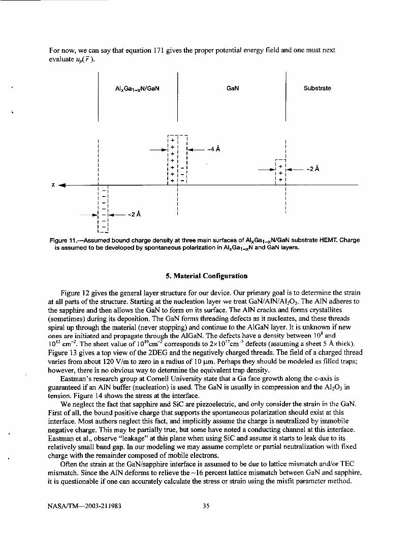
shown in figure 11.
The values of the charges are (from left to right)
C ,5x10_ 2 C , C-8×10⁻² m--T _i- and 2"9 ×10⁻² m-T
These charges are Psb and would contribute to Up(F ) by the first term in equation 177. Assuming
V. PSPON = 0, we have no further contributions from PSPON • We neglect any pyroelectric terms, as no
temperature difference can exist across 4 A.
For the piezoelectric term, we have
Pemzo =d:6=e:S 080)
where the stress/strain may be decomposed into residual, thermal, and lattice mismatch components.It can also include stresses due to metal bonding pads. These terms will be dealt with in a later section.
NASA/TM--2003-211983 34
Fornow,wecansaythatequation171givestheproperpotentialenergyfieldandonemustnextevaluateup( F ).
AIxGal_xN/GaN GaN Substrate
z .11 I
I-II
i-II I
i_1I - I-- I-ql--
I -II Ii._ /
I+
I +I+Ii +I+
I+I
~2A
In.4_ -4 A
I+
I+I
~2b,
Figure11 .---Assumed bound charge densityat three mainsurfacesof AIxGal_xN/GaNsubstrate HEMT. Chargeis assumed to be developed by spontaneouspolarizationin AIxGal_xN and GaN layers.
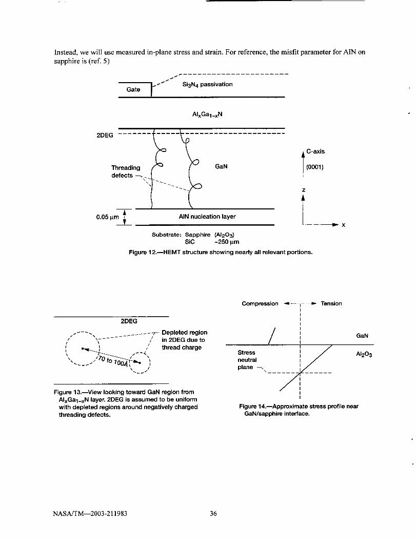
5. Material Configuration
Figure 12 gives the general layer structure for our device. Our primary goal is to determine the strainat all parts of the structure. Starting at the nucleation layer we treat GaN/A1N/AI203. The A1N adheres to
the sapphire and then allows the GaN to form on its surface. The A1N cracks and forms crystallites
(sometimes) during its deposition. The GaN forms threading defects as it nucleates, and these threads
spiral up through the material (never stopping) and continue to the A1GaN layer. It is unknown if newones are initiated and propagate through the A1GaN. The defects have a density between 108 and
1012 cm -2. The sheet value of 10]°cm -2 corresponds to 2x 1017cm-3 defects (assuming a sheet 5 A thick).
Figure 13 gives a top view of the 2DEG and the negatively charged threads. The field of a charged thread
varies from about 120 V/m to zero in a radius of 10 btrn. Perhaps they should be modeled as filled traps;
however, there is no obvious way to determine the equivalent trap density.Eastman's research group at Cornell University state that a Ga face growth along the c-axis is
guaranteed if an A1N buffer (nucleation) is used. The GaN is usually in compression and the A1203 in
tension. Figure 14 shows the stress at the interface.We neglect the fact that sapphire and SiC are piezoelectric, and only consider the strain in the GaN.
First of all, the bound positive charge that supports the spontaneous polarization should exist at this
interface. Most authors neglect this fact, and implicitly assume the charge is neutralized by immobile
negative charge. This may be partially true, but some have noted a conducting channel at this interface.Eastman et al., observe "leakage" at this plane when using SiC and assume it starts to leak due to its
relatively small band gap. In our modeling we may assume complete or partial neutralization with fixed
charge with the remainder composed of mobile electrons.Often the strain at the GaN/sapphire interface is assumed to be due to lattice mismatch and/or TEC
mismatch. Since the A1N deforms to relieve the -16 percent lattice mismatch between GaN and sapphire,
it is questionable if one can accurately calculate the stress or strain using the misfit parameter method.
NASA/TM--2003-211983 35
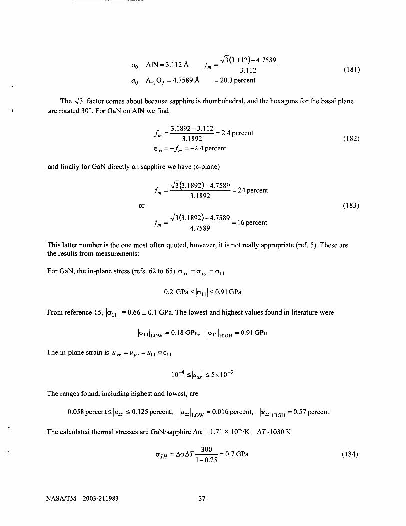
Instead, we will use measured in-plane stress and strain. For reference, the misfit parameter for A1N on
sapphire is (ref. 5)
Gate
.s
,.-'""" Si3N4 passivation
AIxGal_x N
Threading (," _ ( GaN
defects--_"_"\I" -" - "- "" "_
0.05 I_m _ AIN nucleation layer&
T
C-axis
(0001)
z
Substrate: Sapphire (AI203)
SiC -250 I_m
Figure 12.--HEMT structure showing nearly all relevant portions.
x
2DEG
t" -, ...... -z-- Depleted region/ _....... / in 2DEG due to
I _ /
! | // thread charge\ \
Figure 13.reView looking toward GaN region fromAIxGal_xN layer. 2DEG is assumed to be uniformwith depleted regions around negatively charged
The calculated thermal stresses are GaN/sapphire Act = 1.71 x 10"5/1(
300OTH = ActAT - 0.7 GPa
1-0.25
U.._ [HIGH = 0.57 percent
AT-1030 K
(184)
NASA/TM---2003-211983 37
Recallequation50of section 1, and repeated after equation 79 reads
ETxx =---S..
2v --(185)
Using the measured (_11 and letting E = 300 GPa, we fmd
e..: = 0.33 percent
which is within the experimental limits.
For AlxGal_xN, the measured stress and strains are
0.8 GPa _<Crxx< 1.4 GPa
0.016GPa _<Uxx <0.026GPa
0.0012 GPa _<u.. < 0.0057 GPa
Moving up through the structure, we may state that the GaN is seldom intentionally doped, however,the minimum n-type carrier density is in the low 1017cm -3 range. We have discussed the AlxGal_xN/GaNinterface in section 4, and in general, the AI_Ga1__N is in tensile strain. Most often, authors have assumed
the GaN to be fully relaxed, which we will show is not true. The interface between the AlxGal_xN and theSi3N4 passivation layer has not been reported on extensively, however, it is assumed to play an integral
role in the problems presently plaguing the HEMT. It is assumed that the negative charge that supports
the spontaneous polarization is neutralized by adsorbed ions. It is also assumed that donors may bepresent that actually deliver the charge that forms the 2DEG. There is disagreement as to the source of the
2DEG charge. This interface is assumed by some to contain traps that interact with the gate, which causesthe unexplained current collapse when radio frequency is applied. Some attribute the collapse phenomena
to dielectric loss and bulk traps in the Si3N4.
Stress/Strain With Position
This is a most important topic, but unfortunately, not discussed much in the literature. Only one
reference, Demarest (ref. 62), used the standard software package for stress/strain from ANSYS. The
paper shows the strain variation around metal pads on SiO2 layers. It should be mentioned that when GaN
is grown on sapphire and SiC with A1N nucleation layers, polymorphs of Wz and zincblende regions maycoexist. In some cases as much as 25 percent may be zincblende (on an Si wafer). During growth the GaN
is in tension, but during cooling it goes into compression in the basal plane. Misfits form during the entire
process, so the state of strain is highly variable from sample to sample due primarily to the differenttemperatures for growth, cooldown rates, and other factors.
For reference, the basal plane strains at an interface are
e_=_vy = +fro = ± a° -astn3 (186)aSUB
where astm is the lattice constant in the layer in which the strain is sought. The corresponding strain alongthe c-axis is
NASA/TM--2003-211983 38
_. 2 cl3_--=- --_xx (187)C33
For GaN, c,l, and a'[', that is, as c decreases, a increases. The net strain is the combination of lattice
mismatch, thermal mismatch (TEC), and residual strain. The latter often dominates, so we should rely on
measured results as much as possible. For thin layers (up to about 2 _tm), we may assume the stress
is linear (ref. 63). Figure 15 depicts the measured stress for films of GaN on 6H-SiC (by MOCVD). In
the region near 2 _tm the material apparently relaxes and remains in horizontal tension for further growth.
In figure 16 from (ref. 64), which shows the biaxial stress o_ = o_v = o 11 to be negative
(compression).
0o6 --
IX
0,5 n
0.4--
0.3 --
0.2 --/
/
0.1 -- //
//
0.0 _"s
-0.1 :-_'_
--0.2
/ \
//
/ \/
/ \/
/
I I I I0 1 2 3 4
t, _tm
Figure 15.--Measured stress in GaN epilayer grown on 6H-SiC by MOCVD. Note, stress-free region occurs near 0.5 I_m thickness (see ref. 66).
0.50.4
0 0.3
-_ 0.20.10.0 I I I
3010 20
t, I_m
Figure 16.--Reduction in stress with thickness of GaN on sapphire.
Here (rxx = ¢ryy _--_rll which is negative (film in compression).Absolute value is plotted.
This trend is common; GaN on sapphire is often in compression while on SiC it is in tension. This,
however, is not necessary, and the films may be in either state of strain on both substrates. It all depends
on the mode, and temperature of growth, the nucleation layer preparation, the thickness of both the
nucleation layer and the GaN layer, and the crystal orientation of the substrate and its surface condition.
For GaN on sapphire (A1203), it appears that the strain decreases with thickness to some power, or
almost linearly, or exponentially from the AIN layer (refs. 14, 65, 66). Table X gives the vertical strain
with thickness t in _tm (ref. 65).
NASA/TM--2003-211983 39
TABLE X.--STRAIN ALONG THE c-AXIS
VERSUS FILM THICKNESS
t, _tm Strain Fit equation result
1 12.3 12.3
5 7.3 7.3
20 4.6 4.66
60 1.5 3.26
The fit equation is
_: =[12.3×10⁻⁴]t -°.32416
Table XI gives the basal plane compressive stress versus thickness (ref. 14), and it looks almostlinear.
TABLE XI.--MEASURED STRESS VERSUS
FILM TH]CKNESS FROM REF. 14
_m1
Compressive stress, GPA
-0.64
10 -0.59
20 -0.5650 -0.47
(188)
The paper by Detchprohm (ref. 67) shows the vertical (c-axis) strain varies exponentially from the
nucleation surface. The strain does not relax until the layer is about 100 lam thick. This data was taken
with MOCVD and HVPE grown samples (see fig. 17).
ff
{5
5.191
5.185
5.179 I I I I I0 50 100 150 200 250
t, _tm
Figure 17.--Relaxation of c-axis strain for GaN on sapphire.
NASA/TM--2003-211983 40
The c-axis lattice constant was fitted to an exponential
c (z) = 5.185 + (0.006)e -° 0692
then the strain with position is
+)- 5.185"" 5.185
0.006 -0.0692E..-- e
-" 5.185
c in A, z in B (189)
(190)
For Si3N4
Ac
c 2s13
Aa s11 +s12
a
- 1.2GPa < oll _<-0.02 GPa
(191)
6. Band-Gap Issues
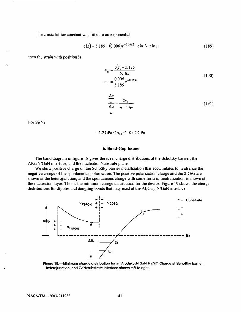
The band diagram in figure 18 gives the ideal charge distributions at the Schottky barrier, the
AIGaN/GaN interface, and the nucleation/substrate plane.We show positive charge on the Schottky barrier metallization that accumulates to neutralize the
negative charge of the spontaneous polarization. The positive polarization charge and the 2DEG are
shown at the heterojunction, and the spontaneous charge with some form of neutralization is shown atthe nucleation layer. This is the minimum charge distribution for the device. Figure 19 shows the charge
distributions for dipoles and dangling bonds that may exist at the AlxGa___N/GaN interface.
+ - - ÷ Substrate
(rPSPON + - (r2DEG
e#Pb + -
+
+
EF
_Ec E1
Figure 18.mMinimum charge distribution for an AIxGal_x N GaN HEMT. Charge at Schottky barrier,
heterojunction,and GaN/substrate interfaceshown left to right.
NASA/TM--2003-211983 41
I
Dipole that increases&Ec
Dipole that decreases &Ec
_ Dangling bonds
1 angling bonds
Figure 19.mDetail of possible chargeconditionsat heterojunction.
The charge state in the AlxGal_xN and the Si3N4 passivation layer are not considered here. The
AlxGal_xN barrier contains A1, but the total charge there is unknown. Often an Si donor layer is placeda few hundred angstroms from the interface to provide the 2DEG carriers. This doping apparently has
a strong effect on the strain state of the barrier, which is a significant source of piezoelectric charge.
We can omit the step discontinuity in _ given in equation 170 of section 4, by combining it with the
step; that is, eA_b + AEc = AE'c . This keeps ¢ continuous, if that causes problems with the software
solvers. While this is convenient, it eliminates the force field of the dipole in the Schrodinger equation.
Recall that the step AEc is due to the absence of available states in the barrier region, and not some form
of repulsive field due to charge. The dangling bonds do not cause a jump in dpand pose no problem.
The range of AEc reported in the literature is about
0.17eV < AE c < 1.8eV (192)
Anderson's model assumes
AEc -- )_AlxGal_xN-- )_GaN (193)
However the uncertainties in Z are very large (refs. 68 and 69)
For GaN 2.1 < Z < 4.26 eV (194)
For AlxGal_x N Z(x) = 3- 4x for x < 0.75 (195)or = 3.25- 2.95x x < 0.75
where OEg/&_l_ = 21 to 27 meV/GPa= 42 meV/GPa for hydrostatic stress (and Si doped)
NASA/TM--2003-211983 43
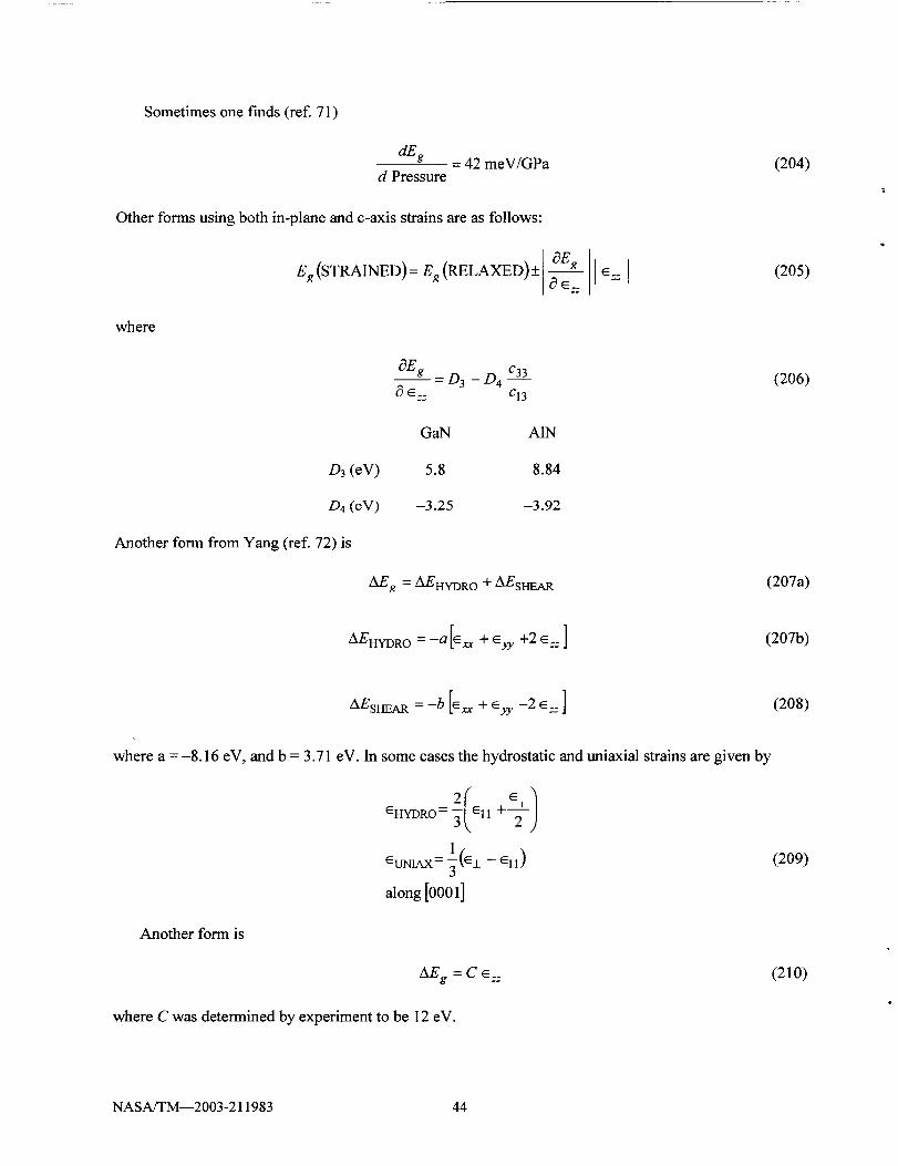
Sometimesone fmds (ref. 71)
dEe' - 42 meV/GPad Pressure
Other forms using both in-plane and c-axis strains are as follows:
Eg (STRAINED)
where
D3 (eV)
D4 (eV)
Another form from Yang (ref. 72) is
= Eg(RELAXED)+ C3Eg _..E... z "
Ogg- D 3 - D 4 c33
E:: C13
GaN A1N
5.8 8.84
-3.25 -3.92
AEg = AEHYDR O + z_kEsHEA R
AEHYDR0 =-a[e_ + _yy +2 ez: ]
AEsrma R =-b [Cx_ +_yy -2%:]
where a = -8.16 eV, and b = 3.71 eV. In some cases the hydrostatic and uniaxial strains are given by
1
- 11)along [0001]
Another form is
AEg = C E ::
where C was determined by experiment to be 12 eV.
(204)
(205)
(206)
(207a)
(207b)
(208)
(209)
(210)
NASA/TM--2003-211983 44
Finally, one finds in terms of stress
in terms of strain
OEg = 10.1-15.4 eV
OEg _ -6.1 eV EII_ 0.0032
= -8.2 to - 13 eV (TENSILE)
= -16 eV el l > 0.0032
(211)
(212)
The expression for AEg in equation 168 in section 4 is that due to hydrostatic stress only.In figure 20 (based on a figure in the literature); we show the energy gap of GaN with in-plane strain.
Some authors claim that the curve is symmetrical, that is, the gap increases for both compression andtension.
e_
e-"I,kl
4.0 --
3.8 --
3.6 --
3.40.00
f
/
fJ
/ It
II
/
,,o 1/
I.s
11I
Is 1
11
I
I I I I I0.01 0.02 0.03 0.04 0.05
qEII
Figure 20.--Vadation of bandgap of GaN with basal plane strainell = exx = eyy(see ref. 73).
Now we consider the change in band gaps with temperature (refs. 73 to 75).
For GaN
T 2
Eg = 3.503 + 5.08 x 10 -4 eVT - 996 K
T 210 -4
or --/_g = 3.509 - 7.32 x eVT + 700 K
or Eg =Eg(T=O)-8.32xlO -4 T2T+836K
eV
(213)
NASA/TM--2003-211983 45
ForAIN
Eg = 6.118-1.8x 10⁻³T 2
T + 1462 KeV
Eg(x,T)=(3.42x +0.068)-8.73×10 -4T 2
T+830KeV
(214)
The band gap of AlxGal_xN is assumed to vary with mole-fraction x as
where the bowing parameter "b" varies from 0.53 to 2.6 eV in the literature. Some have even stated it is 0,
+0.2, or +0.3 eV. The following forms are found.
Eg = 3.43 + 2x + 0.7x 2(216)
= 3.43 + 2.56x
7. Thermal Conductivity
Let K(To) be the thermal conductivity at To (normally 20 °C). Then the variation with temperature is
wK(T)= K(T0 cm K
TABLE XII.--SUMMARIZES THE VALUES
FOR OUR MATERIALS
Material K r
Sapphire 0.25 to 0.50 0.544SiC 3.3 SI, 0.5 0.524
GaN 1.3 to 1.7
Si3N4 0.37
A1N 2.0
Si 2.0
Some experimental results for AIN are below.
TABLE XIII.--THERMAL CONDUCTIVITY
VARIATION WITH TEMPERATURE FOR AIN
T Experimental value for K300 2.85
400 1.80
600 0.96
1000 0.48
NASA/TM--2003-211983 46
8. Orders of Magnitude of Terms and Approximations
The exact form for the potential of a rectangle of charge is given in the appendix. It is tedious so we
will assume the potential of a disc of charge is a reasonable approximation. The potential of a disc ofradius "a" is
°° I_a 2 z 2 ] (218)%(z)- 2%% + -z2
where er0is the surface charge density. Assume the source-drain spacing is 2 _tm, then a = 1 _tm. For thespontaneous polarization at the interface, the effective charge density is
o0 = 5.1x10_ 2 Cm2 (219)
Evaluate at 70 A from the surface
_b(70A) = 320V (220)
This would be the value if no screening existed due to mobile charge. We will assume the screening can
be modeled using the classic Debye-screening factor
fDS = e-= / eD (221)
where eD is the Debye length
_D = - f-_-_
"_29oq (222)C
P0 =n0q =1.6×10⁶ m3
The densities in the 2DEG are on the order of 1019 cm -3, which yields a length of about 8.25 A. The
evaluating point of 70 A is then about 8.5 Debye lengths, and the reduction factor becomes
fDS = 2 x 10⁻⁴ (223)
Thus, the potential is 64 mV, which is well within acceptable limits.
Now we estimate the terms in equation 171 in section 4, to ascertain their relative magnitudes. The
step in the conduction band is bounded as
0.17eV _<AE c < 1.8eV (224)
Therefore, all the other terms should be less than an eV or so. The change in the bandgap due to strain,
AE_, has a large dispersion. From section 6, we fmd
+(70A)= Es (0) (70A)= (4.8)< 108 V/m)(70 × 10 -1° m)
= 3.36 V .'. e+ = -3.36 eV(226)
which is high. If we reduce the field by a factor of 10, which is reasonable, then the value is acceptable.
There are two justifications for the reduction by the factor of 10; one is the uncertainty in the stiffnessparameters while the other is the chosen order of magnitude of the strain. The exchange correlation is
-38.6 meV and the image force gives -0.146 meV. The dangling bond gives
Vab = 20.7n d meV (227)
where nd is the number of bonds. This would give a very large value for even one bond. Using thescreening factor reduces it by 10-4, which brings it into a reasonable range. The dipole contribution gives
-896 eV without screening (for just 100 electrons on a sheet). The screening reduces it to -89.6 meV,which is excellent.
Now we estimate some of the strains that will contribute to Poisson's equation 150 in section 4.
We start with the strains due to metal pads and dielectric films on the AlxGal_xN top surface. Consider asemi-inf'mite film of thickness h on a substrate. The stresses due to this "single edge" (refs. 76 and 77)
(see fig. 21).
-2 fE ( x31 (228),< t..-7-J
h=df
H
h<<HfE = °'fdf
jsf
I"/
/
f/
_ -y
z rl i
: rl"N_ilx I ,z)
Figure 21.--Geometry for calculationof stress in region z _>0. Singlestage at x = 0 developsstressesfor x >__0.
NASA/TM--2003-211983 48
-2vfET2 = t_ yy -
7t
-2f T 3 --t_.. -
T4 =¢_yz =0
T 5 =Gxz --
T6 =_xy =0
These are correct for x > 0. They are not correct for large negative x (which is out of our range).
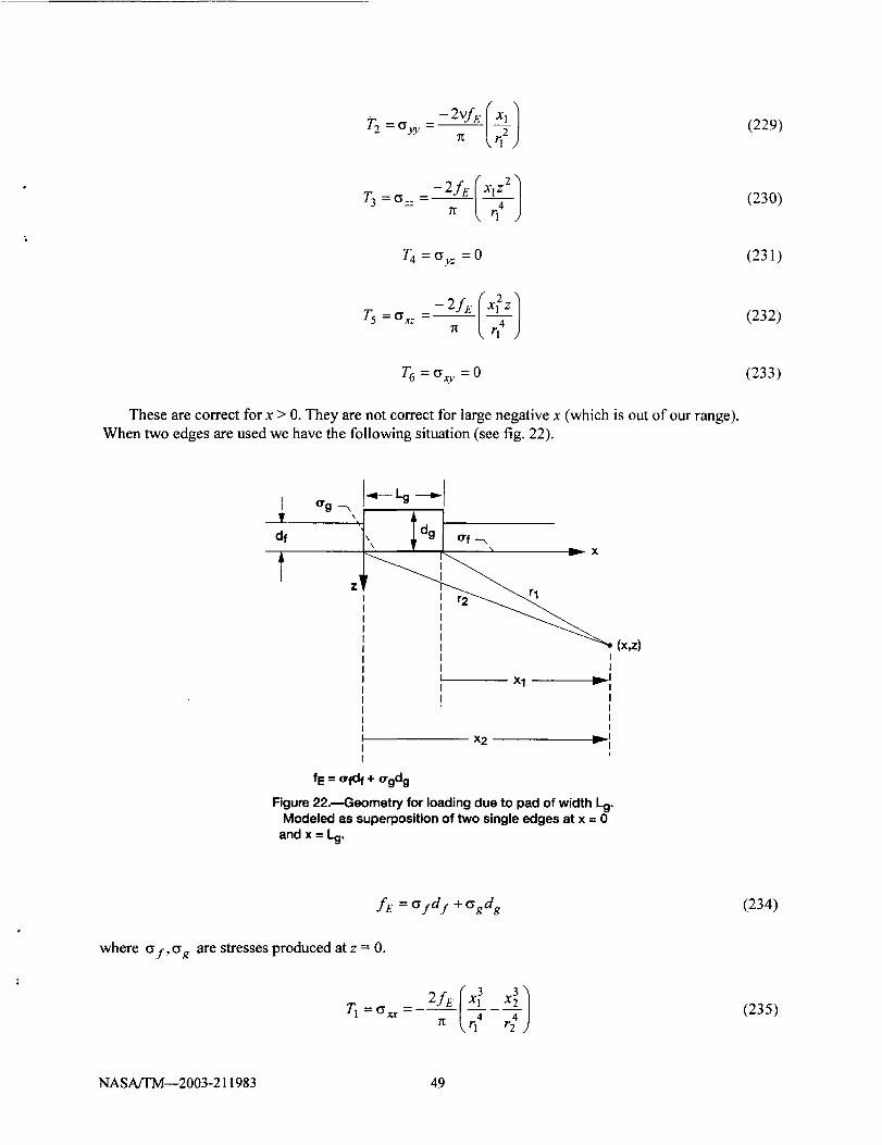
When two edges are used we have the following situation (see fig. 22).
(229)
(230)
(231)
(232)
(233)
df '\ Idg ! of--,,
l Z _ I _ X
II
X1 _'_[
IIII
x2 _1I
fE = °'NIf + _gdg
Figure 22.---Geometry for loading due to pad of width Lg.
Modeled as supe_osition of two single edges at x = 0
and x = Lg.
(x,z)
where of, Crg are stresses produced at z = 0.
T] =G_ --
fE = Old/+ Ggdg (234)
(235)
NASA/TM--2003-211983 49
x2T2 =_yy. - d
T3 =or.. - 2fE ( Xlz2X222
-- _ _ra4 r4
T4 = _yx = 0 (238)
T 6 = CYxy = 0 (240)
This is known as the "effective edge" model. For AlxGal_xN or GaN we have
rl
i ][00000.ilP2 = 0 0 d]5 0 T3 (241)
P3 d31 d3! d33 0 0 T4%
_T6.
P_-- dlsT5 (242)
P2 = 0 (243)
P3 = d31 (T1 + T2 )+ d31T3 (244)
then
Px =d15(@-)( x2--z xlzl (245)<4 4)
Py : 0 (246)
,. --_1(2J_ x_+_'_f2rJ__(Xlx_+d_[2--J_x,z x_z_" k. 7_ .]< I"1 4 < n )_ r, 2 d n r; r_
Notice the coordinate system is not that used in other sections. To conform to that system observe thefollowing changes: z (here) goes to (-z) there, and y (here) goes to (-y) there. Thus, the only changes
required are the signs ofy and z. This has already been done in equations 245 and 247 above.
(236)
(237)
(247)
NASA/TM--2003-211983 50
A previousstudyusingtheaboveequationshasbeendonein theAlxGal_xAs/GaAsheterojunctionsystem(ref.78).It wasobservedthatthestresschangedfromtensionto compressionatthemole-fractionx = 0.03. The crystal type was zincblende (cubic) so
rz/11
[!°°e'4°°°1--o°o°o°0el4u44U55
_U66 _
(248)
Note, only shearing stresses cause ff in this system. If grown in the [100] direction, then P = 0; if grown
in any other direction, then P ¢ 0. For GaAs
v = 0.23
d14 = 2.6× 10-l° cmV
Px = dl4°'zx
(close to GaN) (249)
Py = dl4_ y.z. (250)
----kal,(_--O_) (251)
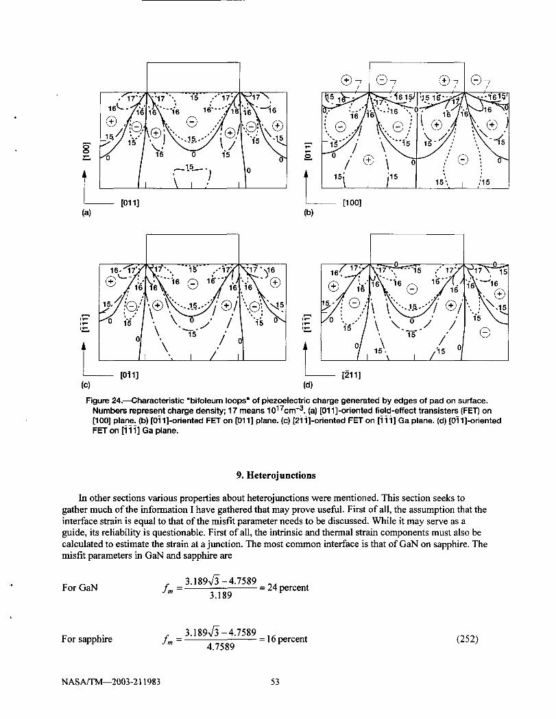
Figure 23 shows qualitatively the differences between the "edge" model and a more accuratecalculation using ANSYS (ref. 79). Figure 24 is from (ref. 80), which shows the piezoelectric charge neara gate pad. Observe the charge density oscillates from positive to negative as one traverses the device on ahorizontal line. The densities are as large as 1017cm -s, which is the same order of magnitude as the
background density obtained in GaN.
NASA/TM--2003-211983 51
O3
EO
t-
¢0¢-
¢0
c"
1018
1017
1016
1015
1014
m
z
m
1013 Io.o o.1
(.-)
_AAAAA
A
q(N d - Na)
Ppz line load
A Ppz FEM
AA
A
A A
(-)
AA _A
A
I I I I0.2 0.3 0.4 0.5
Depth, I_m
Figure23.--Doping profile and piezoelectric charge density Ppzcalculated by "edge" loadline method, and more accurate ANSYS finite element method (FEM) solution.
NASA/TM--2003-211983 52
16('-- --_
-'-. "0
-- [o111(a)
i
,_... ,_ ...h_!(..J_ L7
15 0 15
,,_...15._.....
E
T(b)
@7r@ __,
.---:_e.1_\...:,_"7.,(
I
[_oo]
==
15", I ,;15
IV--
II--
,._-.
®*@ ' _:S"@ '
,s,47: '. . . ..j_!
.\ \.o./..I "-_ 0"- ii ;_ \I o ,\ .I-- [0il] [2111
(c) (d)
Figure 24.mCharacteristic "bifoleum loops" of piezoelectric charge generated by edges of pad on surface.
Numbers represent charge density; 17 means 1017cm-3. (a) [0i 1]-oriented field-effect transisters (FET) on
[100] plane. (b) [0i 1]-oriented FET on [011] plane. (c) [2i 1]-oriented FET on [i i i] Ga plane. (d) [041]-oriented
FET on [111] Ga plane.
9. Heterojunetions
In other sections various properties about heterojunctions were mentioned. This section seeks to
gather much of the information I have gathered that may prove useful. First of all, the assumption that theinterface strain is equal to that of the misfit parameter needs to be discussed. While it may serve as a
guide, its reliability is questionable. First of all, the intrinsic and thermal strain components must also be
calculated to estimate the strain at a junction. The most common interface is that of GaN on sapphire. Themisfit parameters in GaN and sapphire are
It wouldappearthattheGaNwouldbefialateral tension (and thus in vertical compression), and
visa-versa for the sapphire. Experimentally, while GaN is growing on sapphire, it is in tension. The
corresponding TEC are
For GaN ot = 5.59× 10⁻⁶/K
For sapphire tx = 7.3 × 10⁻⁶/K
This implies the GaN would be in compression. Theory would say the thermal stress is
I",l I-- A°tAT E(GaN)l-v
3201 - 0.25
= 0.74 GPa
(253)
Experimentally, the net stress is near 0.66 GPa, compression.The next combination is A1N on sapphire (which is the standard nucleation layer). The misfit
parameters are
For A1N fm _ 13.189 -- 4.75891 _ 53 percent3.112
For sapphire f,, _ ]3.112 -4.7589] _ 35 percent (254)4.7589
The TEC for sapphire is a = 7.3 x 10⁻⁶/°C. It would appear that the A1N is in lateral tension latticewise and
= (-- 0.029-- 0.052X) =:, 3.25X (1013) electrons/cm z
c_Li(PIEZO) GaN = 0.0163x m2
if(total) GaN = PSPON(GaN) + Ppmzo (GaN)
C
=(-0.029 + 0.0163x) m2
(260)
(261 )
(262)
(263)
NASA/TM--2003-211983 55
alxoalxN)--426x( oc2
m
= (2.66 - 3XxX1013 ) electrons/cm 2
p (totalXbothmaterials)=(_8.4x_l.9x2)×lO_6 C2m
C- -0.096x --
m 2
(264)
(264a)
The stiffness coefficients are
C2.6 x 10-2 < P(total) < 4 x 10⁻²
m 2
q3(x) = 5x + 103 - 1lx + 105 GPa
C33 (X) = -32x + 405 GPa
The stress coefficients are (refs. 5, 81, 82)
e31 (x)= -0.1 lx -0.49 --C
m 2
ce33 (x) = -0.73x + 0.73 m2
The relative dielectric constant is
_(x)---0.sx+9.5
The Schottky barrier heights are (ref. 83)
ed_b = (1.3x + 0.84)eV
eO_b= (2.44x + 0.91)eV
The effective masses are
The electric field is
Ni
Ti/Al
me(X)= [O.3x + O.20- x)]m o
mhh(x)=[3.53x + 1.76(1- x)]m 0
(265)
(266)
(267)
(268)
(269)
(270)
(271)
(272)
(273)
(274)
NASA/TM--2003-211983 56
Finally,thesurfacesheetdensityis
e(x) = (7.9x 10⁻⁴ +l.15x 107 x)V/cm
ore(x)=(9.5x + 2.1x2 )x lO6 V/cm
or e(x)= 1.2x x 10 6 V/cm
(275a)
(275b)
(275c)
OTOT(X) = 0.068X _ (276)m 2
ns(X)=6x×lO12 e (277a)cm 2
Orns(X)_ 5.5xxlO13 ecm 2
(277b)
10. Defects
For unintentionally doped AIGaN the cartier density is near 1.017cm 3. The carders are assumed to be
caused by N vacancies, but there is no general agreement. Listed are some speculations on defects.
1. Surface traps cause the radio frequency compression. These are emptied and filled by the gatevoltage. Some speculate that the gate voltage alters the strain in the barrier and passivation
layers and thus the amount of trapped charge.2. Shallow traps cause I-V dc current loops.
3. Deep traps in the buffer are the cause for the I-V dc current collapse. Hot electrons are
introduced into the buffer for drain voltages above 20 V. Gate voltages have no effect on this
process.
A surface donor at 1.4 eV, 1.65 eV.A deep trap at 1.91 eV.
A shallow trap at .95 to 1.0 eV with capture cross-section 4× 10-12cm 2.
For mole-fractions, the density of these traps are:
TABLE XIV.--APPROXIMATE TRAP
DENSITY IN A]xGal_xN
0.05
0.15
0.25
N, cn1-3
5x10¹⁷
2x10 TM
5×10¹⁸
For semi-insulating (SI) GaN a trap exists at 2.15 eV below Ec with density between 3 x 10⁹ and3 x 101° cm -2. For normal GaN, traps at 1.8 and 2.85 eV below Ec. A deep acceptor trap exists at 2.2 eV
below E¢ with density -1 x 101° cm -2.
NASA/TM--2003-211983 57
Thenitrogenvacancyhasastate40meVbelowEc, and the E2 trap exists 0.55 eV below Ec. The trap
that causes dc current collapse is 1.19 eV above Ev. The dominant Mg trap is 150 to 200 meV above Ev.
A trap exists at 0.95 eV above Ev and the characteristic yellow emission is due to a transition betweenlevels 1 eV below E¢ to one 0.2 eV above Ev. The following list gives the levels (I assume with respect
to Ev) of many of the standard impurities found in GaN (ref. 22).
Zn 0.34, 1.8-1.9, 2.2, 2.5-2.6, 2.8
Mg 0.25, 2.95, 3.2 (note, 0.15 to 0.2 in the paragraph above)Cd 0.55, 2.7, 2.85
Be 0.7, 2.2Hg 0.41, 2.9, 2.43
C 0.86, 2.15
Li 0.75, 2.23P 2.85
As 2.58
Si 0.225
11. Amplifiers
The best ever performance: 9.1 W/mm at 10 GHz on 4H-SiC (refs. 84 to 86). The maximum availableis 12 W/ram, for then the channel goes above 300 °C and/or the SiC substrate starts to leak, and largeanomalous current starts.
Devices have been plagued by both dc and tuning-induced failures.
Eastman says degrade most theoreticalf by 30 percent. SiC has maximum thermal dissipation of27.8 W/mm, but starts leaking at 10.9 W/mm. SiC leaks more than sapphire due to smaller bandgap.
Eastman 0.2 < x < 0.4
Channel temperature < 300 °C
P(max) at 10 GHz = 12.5 W/mm
The channel temperature is
rc. czL = r0(StmSrRArE)+ e,jDVz s
Rth = 24[l +(T- To)× lO-3] K'mmW
(MAX)=500K
The devices are predominantly thermally limited, so thermal simulations would be important.
NASA/TM--2003-211983 58
Appendix
I i>_ _"ZO - 1 111>-.. _ I
Figure 25.--Epitaxial AIxGa l_x N layer (z _>0) on GaN (z < 0) with spontaneous
polarization P and bound charge on plane z = 0 and z = z0.
The field due to the spontaneous polarization of the epitaxial layer of AlxGal_xN is developed.Figure 25 gives the geometry. The spontaneous polarization is specified by
PSPON = -Poa: (A1)
Where P0 = 0.08 C/m 2 on the top surface and 0.051 C/m 2 on the bottom surface. This assumes no
neutralization of the negative charge on the top surface due to adsorbed charge. It also models the netcharge at the heterojunction. Starting with the In'st term of equation 176 of section 4
-fi. h ds 'l,ip (_) =
_r
Lr-"'l(A2)
On the upper surface h = -d:, so if- h = -P0. While on the lower surface we have h = --d:, P- h = P0.
Thus, the two surfaces at z = 0 and z = z0 are just uniform charge sheets.On the lower surface we have
where we have used 380.311,261.01,380.001, and 380.111 from reference 87. The second term of
equation (A7) is the negative of equation (A9) with Yo = 0.
On the upper surface we have
?-- ?--
r' = x a x + y ay + z Oa.
: x_+_ +z_:I_-_'1:[(x-x')_+_ -y')_+(_-zo)_l'_
ds'=dx'dy'
(A6)
(A7)
(A8)
(A9)
(AlO)
(All)
(A12)
NASA/TM--2003-211983 60
then
u_ 4_0_0_o ___x/2___y,/2___._0/21'2 (A13)
By observation of equation (A6), we see equation (A 13) only differs by a negative sign and thereplacement ofz 2 with (z-z0)2; thus only minor modifications are necessary on equation (A9), to evaluate
equation (A13). The superposition of the results of equation (A9) and (AI3) constitute the complete
potential of the two sheets of charge. The valid range is yo -<y, and all x and z.
NASA/TM--2003-211983 61
References
.
2.3.
4.
5,
6.
7.
8.9.
10.
11.
12.
13.14.
15.
16.
17.
18.19.
20.
21.
22.
23.
24.25.
26.
27.
28.
29.
B.A. Auld, Acoustic Waves and Fields in Solids (volumes I and II), John Wiley, 1973.
J.F. Nye, Physical Properties of Crystals, Oxford, Clarenden Press, 1957.
C. Deger, et al., "Sound velocity of A1GaN thin films obtained by surface acoustic-wave
measurements," Applied Physics Letters (APL), 71, p. 2400, 1998.M. Eickhoff and O. Ambacher, "Piezoresistivity of AlxGal.xN layers and AlxGal._N/GaN
heterostructures," Journal of Applied Physics (JAP), 90 p. 3383, 2001.O. Ambacher, et al., "Two dimensional electron gases induced by spontaneous and piezoelectric
polarization in undoped and doped A1GaN/GaN heterostructures," JAP, 87, p. 334, 2000.
A. Polian, et al., "Elastic constants of gallium nitride," JAP, 79, p. 3343, 1996.R. Schwarz, et al., "Elastic moduli of gallium nitride," APL, 70, p. 1122, 1997.
B. Foutz, http://iiiv.tn.cornell.edtL/www/foutz/nitride.html
Hughes and Gaylord, Basic Equations of Engineering Science, Schaum's Outline Series,McGraw-Hill, 1964.
C. Kisielowski, et al., "Strain-related phenomena in GaN thin films," Phys. Rev. B, 54, p. 17745,1996.
N. Maeda, et al., "Two-dimensional electron-gas density in AIGaN/GaN heterostructure field-
effect transistors," APL 73, p.1856, 1998.E. Etzkorn and D. Clarke, "Cracking of GaN films," JAP, 89, p. 1025, 2001.
B. Skromme, et al., "Strain determination in heteroepitaxial GaN," APL, 71, p. 829, 1997.T. Kozawa, et al., "Thermal stress in GaN epitaxial layers grown on sapphire substrates," JAP,
77, p. 4389, 1995.S. Hearne, et al., "Stress evolution during metalorganic chemical vapor deposition of GaN," APL,
74, p. 356, 1999.
M. Mynbaeva, et al., "Strain relaxation in GaN layers grown on porous GaN sublayers," MRSInter. Jour. Nitride Semicond. Res. 4, 14, 1999.
G. Olsen and M. Ettenberg, "Calculated stresses in multilayered heteroepitaxial structures," JAP,
48, p. 2543, 1977.
N. Itoh, et al., "Study of cracking mechanism in GaN/a-AI203 structure," JAP, 58, p. 1828, 1985.S. Pearton, et al., "GaN Electronics," Advanced Materials, 12, p. 1571, 2000.
H. Morkoc, et al., "Polarization effects in nitride semiconductor device structures and
performance of modulation doped field effect transistors," Solid-State Electronics, 43, p. 1753,1999.
H. Morkoc, et al., "GaN-based modulation doped FETs and UV detectors," Solid-State
Electronics, 46, p. 157, 2002.
H. Morkoc, et al., "Large-band-gap SiC, III-V nitride, and II-VI ZnSe-based semiconductor
H. Jaffe and D. Berlincourt, "Piezoelectric Transducer Materials," Proc. IEEE, 53, p. 1372, 1965.
S. Muensit, et al., "Shear piezoelectric coefficients of gallium nitride and aluminum nitride,"APL, 75, p. 3965, 1999.
A. Wright, "Elastic properties of zinc-blende and wurtzite A1N, GaN, and INN," JAP, 82, p. 2833,1997.
P. Ramvall, et al., "Influence of a piezoelectric field of the electron distribution in a doubleGaN/AlxGal_xN heterojunction," APL, 74, p. 3866, 1999.
J. Im, et al., "Reduction of oscillator strength due to piezoelectric fields in GaN/AlxGa_./Nquantum wells," Phys Rev B, 57, p. R9435, 1998.
A. Durelli, E. Phillips, and C. Tsao, Introduction to the Theoretical and Experimental Analysis ofStress and Strain, McGraw-Hill, 1958.
NASA/TM--2003-211983 62
30.
31.
32.
33.
34.
35.
36.
37.
38.
39.40.
41.
42.
43.44.45.
46.
47.
48.
49.
50.
51.
52.53.
54.
55.
F.Bernardini,etal.,"Spontaneouspolarizationandpiezoelectricconstantsof III-V nitrides,"Phys.Rev.B,56,p.R10024,1997.F.BernardiniandV.Fiorentini,"Polarization-BasedCalculationoftheDielectricTensorof PolarCrystals,"Phys.Rev.Lttrs.,79,p.3958,1997.F.BemardiniandV. Fiorentini,"Macroscopicpolarizationandbandoffsetsatnitrideheterojunctions,"Phys.Rev.B,57,p.R9427,1998.F.BernardiniandV. Fiorentini,"SpontaneousVersusPiezoelectricPolarizationin III-V Nitrides:ConceptualAspectsandPracticalConsequences,"Phys.StatusSolidi,(b)216,p.391,1999.F.BernardiniandV. Fiorentini,"Polarizationfieldsinnitridenanostructures:10pointstothinkabout,"AppliedSurfaceScience,166,p.23-29,Oct.9,2000.O.Ambacher,etal.,"Roleof SpontaneousandPiezoelectricPolarizationInducedEffectsinGroup-IIINitrideBasedHeterostructuresandDevices,"Phys.StatusSolidi,(b),216,p.381,1999.J.Garrido,etal.,"PolarizationFieldDeterminationinAIGaN/GaNHFETs,"Phys.StatusSolidi,(a),176,p. 195,1999.R.Resta,"Macroscopicpolarizationincrystallinedielectrics,"Rev.Mod.Phys.,66,p.899,1994(seep. 912).A.Hangleiter,"Opticalpropertiesandpolarizationfieldsin thenitrides,"J.of Luminescence,87-89,p. 130,2000(seep. 132).R.Martin,"Piezoelectricity,"Phys.Rev.B,5, p. 1607, 1972 (see p. 1611).S. Park, et al., "Comparison of zinc-blende and Wurtzite GaN semiconductors with spontaneous
polarization and piezoelectric field effects," JAP, 87, p. 353, 2000.
Fafara, et al., "Collective and Molecular Modes in Ferroelectric and Antiferroelectric Liquid
Crystals," IEEE Trans. Dielectrics and Electrical Insulation, 8, p. 477, 2001.F. Sacconi, et al., "Spontaneous and Piezoelectric Polarization Effects on the Output
Characteristics ofA1GaN/GaN Heterojanction Modulation doped FETs," IEEE Trans. Electron
Devices, 48, p. 450, 2001.B. Streetman, Solid State Electronic Devices, Prentice Hall, 1990, p. 115.
W. Liu, Handbook oflll-VHeterojunction Bipolar Transistors, John Wiley, p. 127, 1998.M. Lundstrom and R. Schuelke, "Modeling Semiconductor Heterojunctions in Equilibrium,"
Solid-State Electronics, 25, p. 683, 1982.
A. Chatterjee and A. Marshak, "Theory of Abrupt Heterojunctions in Equilibrium," Solid-StateElectronics, 24, p. 1111, 1981.
A. Marshak and K. van Vliet, "Electrical Current in Solids With Position-Dependent BandStructure," Solid-State Electronics, 21, p. 417, 1978.
F. Stem and S. Sarma, "Electron energy levels in GaAs-Gal./Alx As heterojunctions," Phys Rev
B, 30, p. 840, 1984.
H. Unlu and A. Nussbaum, "Band Discontinuities as Heterojunction Device Design Parameters,"IEEE Trans. Electron Devices, 33, p. 616, 1986.
Jogai, "Free electron distribution in AIGaN/GaN heterojunction field-effect transistors," JAP, 91,p. 3721, 2002.L. Van Ruyven, et al., "Optical Phenomena in Ge-GaP Heterojtmctions," Solid-State Electronics,
8, p. 631, 1965.W. Harrison, "Elementary theory of heterojunctions," J. Vac. Sci. Tech., 14, p. 1016, 1977.
R. Grant, et al., "Observation of the Orientation Dependence of Interface Dipole Energies inGe-GaAs," Phys. Rev Lttrs, 40, p. 656, 1978.
W. Frensley and H. Kroemer, "Theory of the energy-band lineup at an abrupt semiconductorheterojunction," Phys. Rev B, 16, p. 2642, 1977.
G. Baraff, et al., "Self-Consistent Calculation of the Electronic Structure at an Abrupt GaAs-GeInterface," Phys Rev Lttrs, 38, p. 237, 1977.
NASA/TM--2003-211983 63
56.
57.
58.
59.60.61.62.
63.
64.
65.
66.
67.
68.69.
70.
71.
72.
73.
74.
75.
76.
77.78.
79.
80.
81.
W.Pickett,etal., "Ge-GaAs (100) Interface: A Self-Consistent Calculation of Interface States
and Electronic Structure," Phys Rev Lttrs, 39, p. 109, 1977.
J. Donnelly and A. Milnes, "The Capacitance ofp-n Heterojunctions Including the Effects ofInterface States," IEEE Trans. Electron Devices, 14, p. 63, 1967.
H. Stormer, et al., "Two-Dimensional Electron Gas at a Semiconductor-Semiconductor
Interface," Solid-State Comm., 29, p. 705, 1979.
W. Hauser, Introduction to the Principles of Electromagnetism, Addison-Wesley, p. 125, 1971.W. Smythe, Static and Dynamic Electricity 2nd Ed., p. 14, McGraw-Hill, 1950.
J. Reitz and F. Milford, Foundations of Electromagnetic Theory, Addison-Wesley, p. 70, 1960.Demarest, et al., "Nanoscale characterization of stresses in semiconductor devices by quantitative
electron diffraction," APL, 77, p. 412, 2000.
N. Edwards, et al., "Trends in residual stress for GaN/A1N/6H-SiC heterostructures," APL 73,
p. 2808, 1998.E. Valcheva, et al., "Elimination ofnonuniformities in thick GaN films using metalorganic
chemical vapor deposited GaN templates," JAP, 90, p. 6011,2001.
Reynolds, et al., "Strain variation with sample thickness in GaN grown by hydride vapor phaseepitaxy," JAP, 88, p. 1460, 2000.
W. Li, et al., "Residual strain in GaN epilayers grown on sapphire and (6H)SiC substrates," APL,
68, p. 2705, 1996.T. Detchprohm, et al., "Relaxation Process of the Thermal Strain in the GaN/-A1 OHeterostructure and Determination of the Intrinsic Lattice Constants of GaN Free From the
Strain," Japanese JAP, p. L1454, 1992.S. Grabowski, et al., "Electron affmity of AlxGal.xN (0001) surfaces," APL 78, p. 2503, 2001.
P. Bridger, et al., "Measurement of induced surface charges, contact potentials, and surface states
in GaN by electric force microscopy," APL, 74, p. 3522, 1999.M. Nardelli, et al., "Strain effects on the interface properties of nitride semiconductors," Phys
Rev B, 55, p. R7323, 1997.P. Perlin, et al., "Pressure studies of gallium nitride: Crystal growth and fundamental electronic
properties," Phys. Rev. B, 45, p. 13307, 1992.
T. Yang and M. Kim, "Screening and strain effects on the ground-state energy of quasi-two-dimensional quantum well system," JAP, 89, p. 1156, 2001.
Z. Yang and Z. Xu, "Electronic and optical properties of unstrained and strained Wurtzite GaN,"
Phys. Rev. B, 54, p. 17577, 1996.T. Zheleva, "Thermal mismatch stress relaxation via lateral epitaxy in selectively grown GaN
structures," APL, 74, p. 2492, 1999.
R. Passler, "Parameter Sets Due to Fittings of the Temperature Dependencies of FundamentalBandgaps in Semiconductors," Phys. Status Solidi, (b) 216, p. 975, 1999.
S. Wong, et al., "Analytic solution of stress distribution under a thin film edge in substrates,"
APL, 79, p. 1628, 2001.S. Hu, "Film-edge-induced stress in silicon substrates," APL, 32, p. 5, 1978.
P. Asbeck, et al., "Piezoelectric Effects in GaAs FET's and Their Role in Orientation-Dependent
Device Characteristics," IEEE Trans. Electron Devices, 31, p. 1377, 1984.
J. Ramirez, et al., "Development and Experimental Verification of a Two-Dimensional NumericalModel of Piezoelectrically Induced Threshold Voltage Shifts in GaAs MESFET's," IEEE Trans.
Electron Devices, 35, p. 1232, 1988.T. Onodera and H. Nishi, "Theoretical Study of the Piezoelectric Effect on GaAs MESFET's on
(100), (011), and (111) Ga, and (111) As Substrates," IEEE Trans. Electron Devices, 36, p. 1580,1989.
Danielsson, et al., "The influence of band offsets on the IV characteristics for GaN/SiC
heterojunctions," Solid State Electronics, 46, p. 827, 2002.
L. Eastman, et al., "Undoped AIGaN/GaN HEMTs for Microwave Power Amplification," IEEE
Trans. Electron. Devices, 48, p. 479, 2001.Y. Wu, et al., "Very-High Power Density AIGaN/GaN HEMTs," IEEE Trans. Electron Devices,
48, p. 586, 2001.
H. Dwight, Tables of Integrals and other Mathematical Data, Macmillan, 1961.
NASA/TM--2003-211983 65
REPORT DOCUMENTATION PAGE Form ApprovedOMBNO.0704-0188
Public reporting burden for this collection of information is esttmatad to average 1 hour per response, including the time for revtewlng instructtons, searching extstmg data sources,gathermg and maintaining the data needed, and completing and reviewing the collectton of information Send comments regarding this burden estimate or any other aspect of thincollection of information, including suggestions for reducing this burden, to Washington Headquarters Services, Directorate for Information Operations and Reports, 1215 JeffersonDavis Highway, Su=te 1204, Arlington, VA 22202-4302, and to the Offtce of Management and Budget, Paperwork Reduction Project (0704-0188), Washmgton, DC 20503
1. AGENCY USE ONLY (Leave blank) 2. REPORT DATE 3. REPORT TYPE AND DATES COVERED
February 2003 Technical Memorandum
4. TITLE AND SUBTITLE 5. FUNDING NUMBERS
Basic Equations for the Modeling of Gallium Nitride (GaN) High Electron
Mobility Transistors (HEMTs)
6. AUTHOR(S)
Jon C. Freeman
7. PERFORMING ORGANIZATION NAME(S) AND ADDRESS(ES)
National Aeronautics and Space Administration
John H. Glenn Research Center at Lewis Field
Cleveland, Ohio 44135-3191
9. SPONSORING/MONITORING AGENCY NAME(S) AND ADDRESS(ES)
National Aeronautics and Space Administration
Washington, DC 20546-0001
WBS-22-755-12-27
8. PERFORMING ORGANIZATION
REPORT NUMBER
E-13653
10. SPONSORING/MONITORING
AGENCY REPORT NUMBER
NASA TM--2003-211983
11. SUPPLEMENTARY NOTES
Responsible person, Jon C. Freeman, organization code 5620, 216--433-3380.
12a. DISTRIBUTION/AVAILABILITY STATEMENT
Unclassified - Unlimited
Subject Categories: 33, 76 and 31 Distribution: Nonstandard
Available eleclronically at http://gltrs.grc.nasa.gov
This publication is available from the NASA Center for AeroSpace Information, 301-621_)390.
12b. DISTRIBUTION CODE
13. ABSTRACT (Maximum 200 words)
Gallium nitride (GaN) is a most promising wide band-gap semiconductor for use in high-power microwave devices. It
has functioned at 320 °C, and higher values are well within theoretical limits. By combining four devices, 20 W has
been developed at X-band. GaN High Electron Mobility Transistors (HEMTs) are unique in that the two-dimensional
electron gas (2DEG) is supported not by intentional doping, but instead by polarization charge developed at the inter-
face between the bulk GaN region and the A1GaN epitaxial layer. The polarization charge is composed of two parts:
spontaneous and piezoelectric. This behavior is unlike other semiconductors, and for that reason, no commercially
available modeling software exists. The theme of this document is to develop a self-consistent approach to developing
the pertinent equations to be solved. A Space Act Agreement, "Effects in A1GaN/GaN HEMT Semiconductors" with
Silvaco Data Systems to implement this approach into their existing software for III-V semiconductors, is in place