66
Basic Fundamentals of Solar Cell Semiconductor Physics for High School Level Physics
| Date post: | 30-Dec-2015 |
| Category: |
Documents |
| Upload: | vincent-matthews |
| View: | 225 times |
| Download: | 3 times |
Basic Fundamentalsof
Solar Cell Semiconductor Physicsfor
High School Level Physics

Review Topics

Wavelength and Frequency
Period (sec)
time
amplitude
Frequency () = 1/Period [cycles/sec or Hertz]Wavelength () = length of one Period [meters]For an electromagnetic wave c = ,where c is the speedof light (2.998 x 10⁸ m/sec)
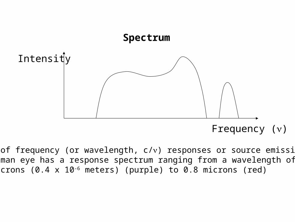
Spectrum
Frequency ()
Range of frequency (or wavelength, c/) responses or source emissions.The human eye has a response spectrum ranging from a wavelength of 0.4 microns (0.4 x 10⁻⁶ meters) (purple) to 0.8 microns (red)
Intensity
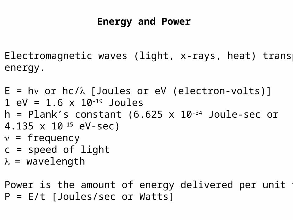
Energy and Power
Electromagnetic waves (light, x-rays, heat) transport energy.
E = h or hc/[Joules or eV (electron-volts)]1 eV = 1.6 x 10⁻¹⁹ Joulesh = Plank’s constant (6.625 x 10⁻³⁴ Joule-sec or4.135 x 10-15 eV-sec) = frequencyc = speed of light= wavelength
Power is the amount of energy delivered per unit time.P = E/t [Joules/sec or Watts]

Photons
A light particle having energy. Sunlight is a spectrum of photons. X-rays and heat are photons also.
Photon EnergyE = h or hc/[Joules or eV (electron-volts)]
(higher frequency = higher energy)
(lower energy)

Irradiance
Amount of power over a given area, Watts/m2
Area = 2.00 m2
4 red photons every second
Energy of 1 red photon = hc/ = (6.63 x 10⁻³⁴ J-s)(2.99 x 10⁸ m/s)/(0.80 x 10-6 meters) = 2.48 x 10⁻¹⁹ J = 1.55 eVIrradiance = Power/Area = (4 photons/sec)(Energy of 1 photon)/2.00 m2
= 4.96 x 10⁻¹⁹ W/m2 Typical sunlight irradiance is 0.093 W/cm2 = 930 W/m2 at = .55 m

Solar Spectrum at Earth Surface (noon time)
E (eV) = hc/ = hc/E
Visable range.75 m (red) - .4 m (purple)1.6 eV - 3.1 eV
Solar Spectrum at Earth Surface.5 eV - 3.6 eVm (infrared) - 0.34 m (ultraviolet)
visible
ultravioletinrfared
Solar Spectrum at Earth Surface
(noon time)
925 W/m2
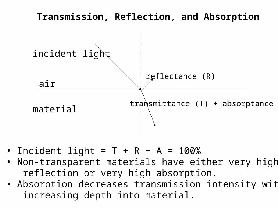
Transmission, Reflection, and Absorption
air
material
incident light
reflectance (R)
transmittance (T) + absorptance (A)
• Incident light = T + R + A = 100%• Non-transparent materials have either very high reflection or very high absorption.• Absorption decreases transmission intensity with increasing depth into material.

Polarization
Unpolarized light(e.g. sunlight) Linearly polarized light
Polarizer
Only one plane of vibration passes
Basics of Semiconductor Physics

Semiconductor Crystal Lattice
Simple Cubic Structure
atomcovalent bond
Silicon has a more complex lattice structurebut a lattice structure exists nevertheless.
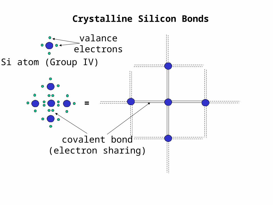
Si atom (Group IV)
Crystalline Silicon Bonds
covalent bond(electron sharing)
=
valanceelectrons

Breaking of Covalent Bond CreatingElectron-Hole Pair
Si atom
covalent bond+
e-free electron movingthrough lattice
created hole(missing electron)
Photon (light, heat)
Photon hits valance electron with enough energy tocreate free electron
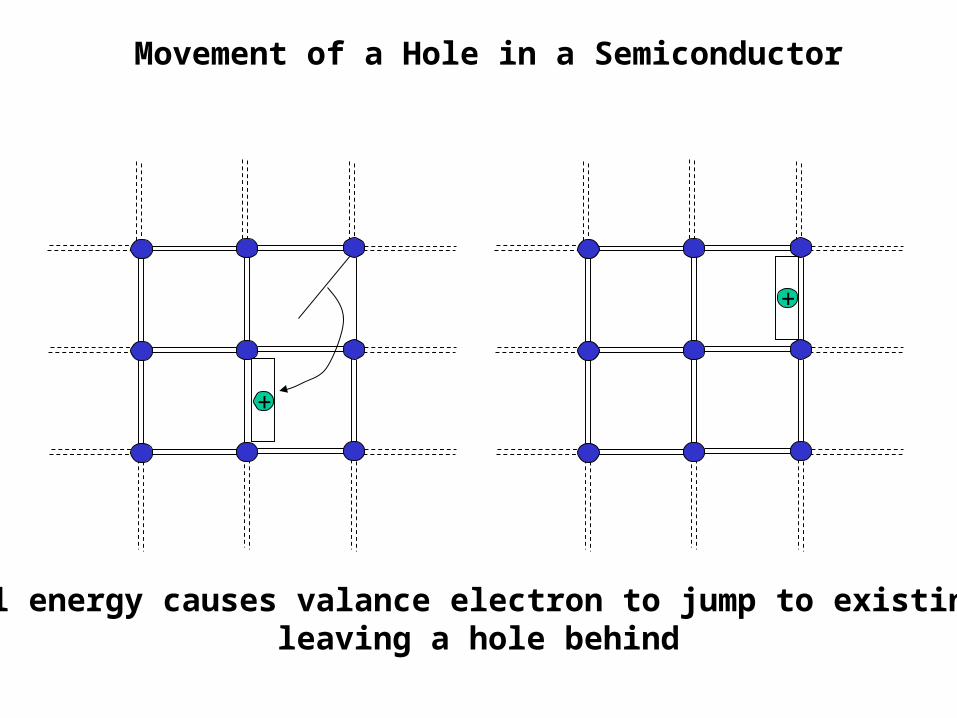
Movement of a Hole in a Semiconductor
+
Thermal energy causes valance electron to jump to existing holeleaving a hole behind
+
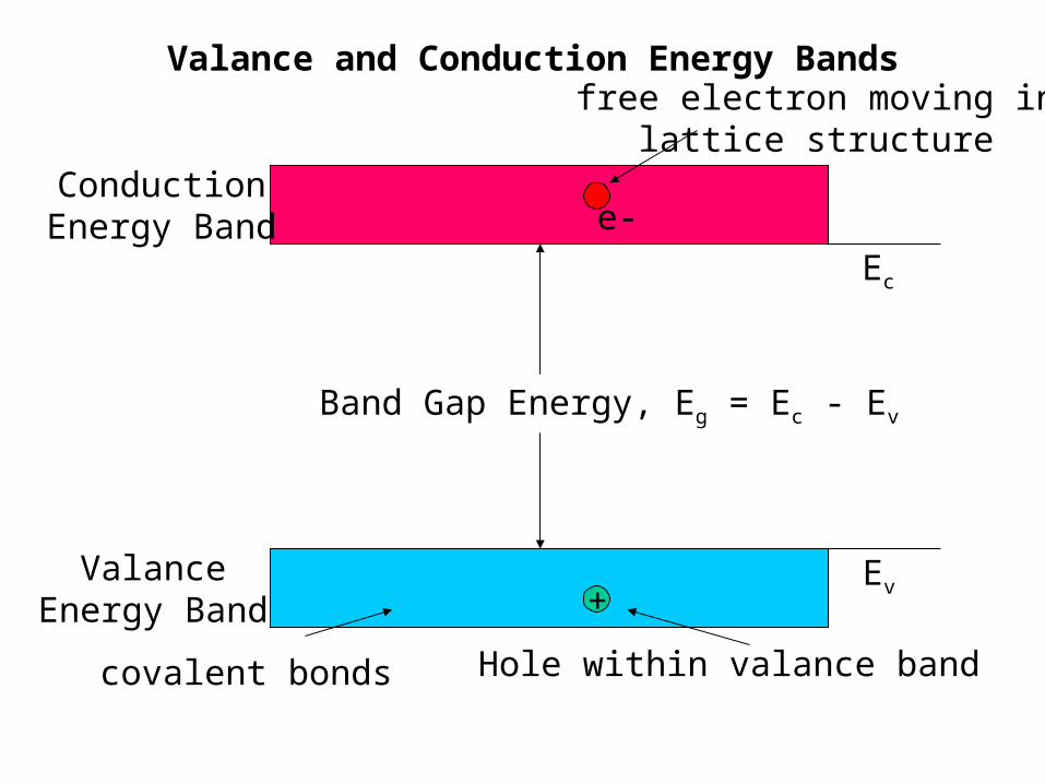
Valance and Conduction Energy Bands
covalent bonds
+
e-
free electron moving inlattice structure
ConductionEnergy Band
ValanceEnergy Band
Band Gap Energy, Eg = Ec - Ev
Hole within valance band
Ec
Ev

Valance and Conduction Energy BandsThermal Equalibrium
covalent bonds
+
e-
free electron withinlattice structure
Heat energyabsorbed
Energy absorbed = Energy given up
ConductionEnergy Band
ValanceEnergy Band
Eg
Hole created within valance band
+
e-
Heat enerygiven up
Ec
Ev
free electron combineswith hole
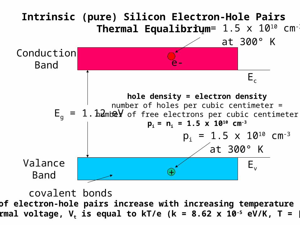
Intrinsic (pure) Silicon Electron-Hole PairsThermal Equalibrium
covalent bonds
+
e-
ni = 1.5 x 1010 cm-3
at 300° K
•Number of electron-hole pairs increase with increasing temperature•The thermal voltage, Vt is equal to kT/e (k = 8.62 x 10⁻⁵ eV/K, T = [Kelvin])
ConductionBand
ValanceBand
Eg = 1.12 eV
pi = 1.5 x 1010 cm-3
at 300° K
hole density = electron densitynumber of holes per cubic centimeter =
number of free electrons per cubic centimeterpi = ni = 1.5 x 1010 cm-3
Ec
Ev

Creating a Semiconductor

Doping or Substitutional ImpuritiesGroup V Atom (Donor or N-type Doping)
Si atom (Group IV)
covalent bond
e-
The donor electron is not part of a covalent bond soless energy is required to create a free electron
Phospherous (Group V)
P atom

Energy Band Diagram of Phospherous Doping
covalent bonds
+
e-
N-type Semiconductor
ConductionBand
ValanceBand
Eg
n > p (more electrons in conduction band)A small amount of thermal energy (300° K) elevatesthe donor electron to the conduction band
Donor ElectronEnergy
e-
intrinsic hole
intrinsic free electron donor free electron
Ec
Ev
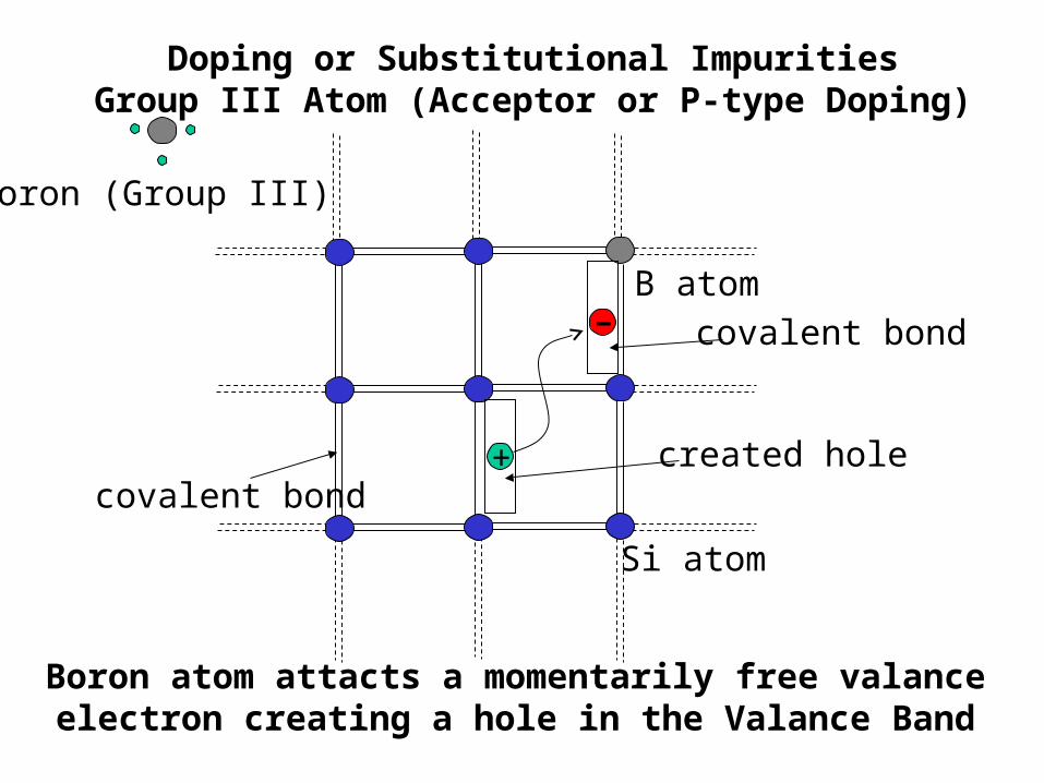
Doping or Substitutional ImpuritiesGroup III Atom (Acceptor or P-type Doping)
Si atom
covalent bond
Boron (Group III)
B atom
+
- covalent bond
created hole
Boron atom attacts a momentarily free valanceelectron creating a hole in the Valance Band

Energy Band Diagram of Boron Doping
covalent bonds
+
e-
P-type Semicondutor
ConductionBand
ValanceBand
Eg
p > n (more holes in valance band)A small amount of thermal energy (300° K) elevatesthe acceptor electron to the Acceptor band
Acceptor ElectronEnergy e-
intrinsic hole
intrinsic free electron
acceptor electron
+
created hole
Ec
Ev

Charge Transport Mechanismswithin a Semiconductor
• Drift Current Density• Diffusion Current Density

y
x
+
Current The number of holes or electrons passing through
a cross sectional area, A, in one second
+ +
++
+
+
+
+
Applied Electric Field
e-
e-e-
e-
e-e-
e-
I = q/t[I] = [coulombs/sec] = [amps]
e-
e-
and Direction of Current
• holes move in Current direction• electrons move in opposite direction

y
x
+
Current DensityThe number of holes or electrons passing through
a cross sectional area, A, in one second divided by A
A (area) = xy cm2
+ +
++
+
+
+
+
Applied Electric Field
e-
e-e-
e-
e-e-
e-
I (amps) = coulombs/secJ (current density) = I/A[J] =[amps/cm2]
e-
e-
and Direction of Current

Drift VelocityThe average velocity of a hole (vp) or electon (ve) moving
through a conducting material
Applied Electric Field
• Scattering Sites are caused by impurities and thermal lattice vibrations• Electrons typically move faster than holes (ve>vp)
+e-
Scattering Sitesvp = dp/t1
ve = dn/t1
dp
dn

Drift Velocity and Applied Electric Field
Newton’s Second Law of MotionF = ma
Analogy with Electic Fieldsm q (mass charge)a E (accelerating field applied electric field)
F = qE
Without scattering sites, the charged particlewould undergo a constant acceleration.
Scattering sites create an average drift velocity.Similar to the terminal velocity of a falling object caused by air friction.
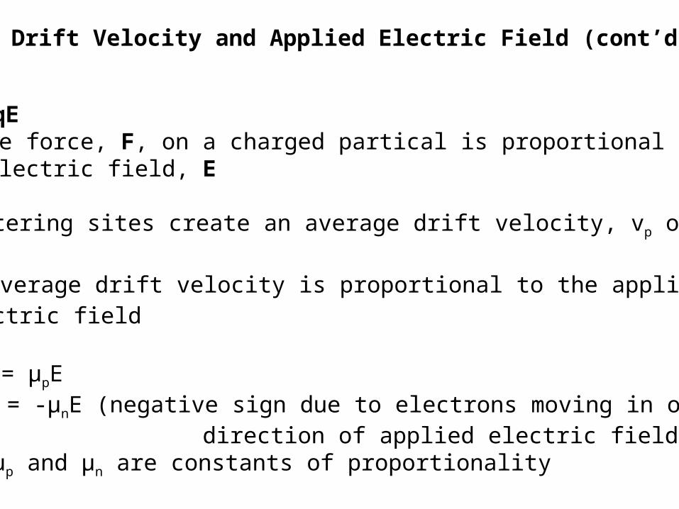
Drift Velocity and Applied Electric Field (cont’d)
• F = qE• The force, F, on a charged partical is proportional to the electric field, E
• Scattering sites create an average drift velocity, vp or ve
• The average drift velocity is proportional to the applied electric field
• vp = μpE• ve = -μnE (negative sign due to electrons moving in opposite direction of applied electric field)
where μp and μn are constants of proportionality
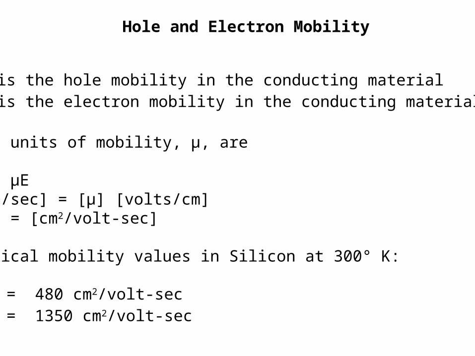
Hole and Electron Mobility
μp is the hole mobility in the conducting materialμn is the electron mobility in the conducting material
The units of mobility, μ, are
v = μE[cm/sec] = [μ] [volts/cm][μ] = [cm2/volt-sec]
Typical mobility values in Silicon at 300° K:
μp = 480 cm2/volt-secμn = 1350 cm2/volt-sec

Mobility and Current Density Relation
CurrentI = q/tq = number of charged particles passing through a cross sectional areat = timeCurrent DensityJ = I/A = (q/t)/AA = cross sectional area
p = number of holes per cubic centimeter (hole density [1/cm3])n = number of electrons per cubic centimeter (electron density [1/cm3])
Each hole has an average velocity of vp
Each electron has an average velocity of ve
++
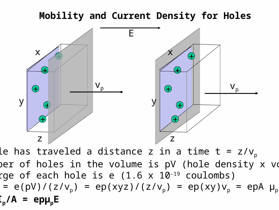
Mobility and Current Density for Holes
Each hole has traveled a distance z in a time t = z/vp
The number of holes in the volume is pV (hole density x volume)The charge of each hole is e (1.6 x 10⁻¹⁹ coulombs)I = q/t = e(pV)/(z/vp) = ep(xyz)/(z/vp) = ep(xy)vp = epA μpEJp|drf = Ip/A = epμpE
E
x
y
z
x
y
z
vp+
+
+
+
+
+
+
+
vp

veve
e-
e-
Mobility and Current Density for Electrons
Replacing p with n and vp with ve gives:The charge of each electron is -e (-1.6 x 10⁻¹⁹ coulombs)I = q/t = -epV/(z/ve) = -ep(xyz)/(z/ve) = -ep(xy)ve = -epA(-μnE)I = epA(μnE)Jn |drf = In/A = enμnE
Ex
y
z
x
y
z
e-
e-e-
e-
e-
e-
e-e-

Drift Current Density Expressions
Jp|drf = Ip/A = enμpEJn|drf = In/A = enμnE
Jp|drf and Jn|drf are in same direction
Total Drift Current = Jp|drf + Jn|drf

Diffusion Process
gas filled chamber empty chamber
sealed membrane After seal is broken
Gas molecules move from high concentration region to lowconcentration region after membrane is broken
If gas molecules are replaced by charge then a current existsduring charge transport creating a Diffusion Current
gas

Electron Diffusion Current
distance
Ele
ctro
n co
ncen
trat
ion,
n
electron flow
Electron diffusioncurrent density
x
slope = n/x
• electron flow is from high to low concentration (-x direction)• electron diffusion current density is in positive x direction• Jn|dif = eDnn/x where Dn is the electron diffusion constant
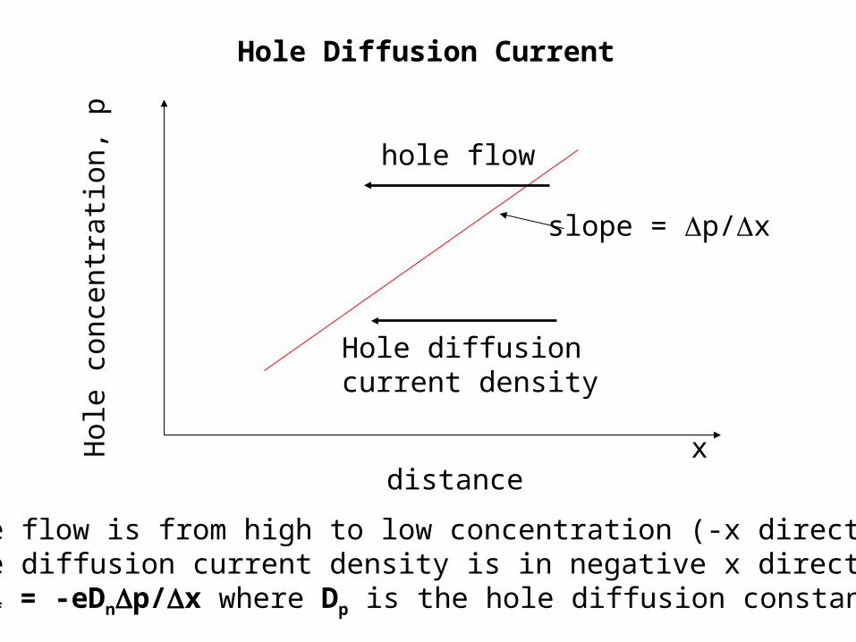
Hole Diffusion Current
distance
Hol
e co
ncen
trat
ion,
p hole flow
Hole diffusioncurrent density
x
slope = p/x
• hole flow is from high to low concentration (-x direction)• hole diffusion current density is in negative x direction• Jp|dif = -eDnp/x where Dp is the hole diffusion constant
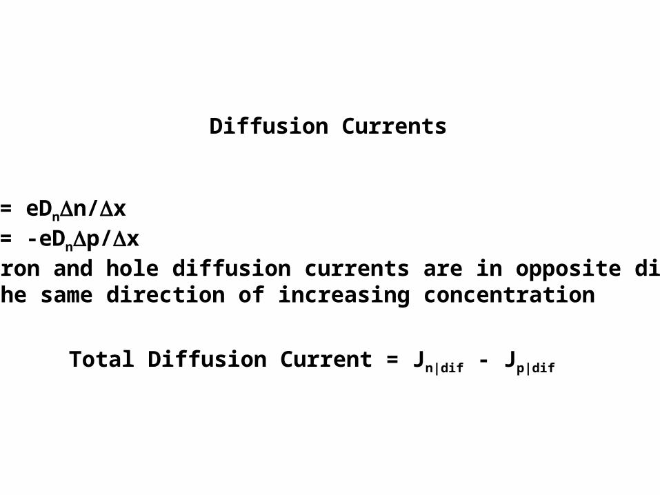
Diffusion Currents
• Jn|dif = eDnn/x• Jp|dif = -eDnp/x• Electron and hole diffusion currents are in opposite directions for the same direction of increasing concentration
Total Diffusion Current = Jn|dif - Jp|dif

Formation and Basic Physicsof
PN Junctions
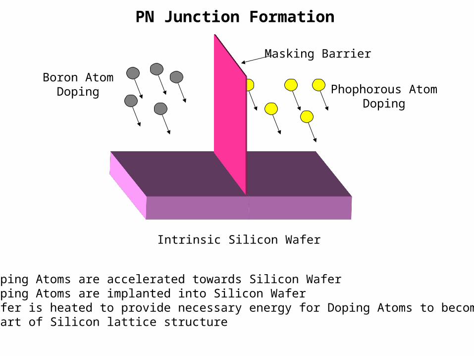
PN Junction Formation
Phophorous AtomDoping
• Doping Atoms are accelerated towards Silicon Wafer• Doping Atoms are implanted into Silicon Wafer• Wafer is heated to provide necessary energy for Doping Atoms to become part of Silicon lattice structure
Intrinsic Silicon Wafer
Masking Barrier
Boron AtomDoping

PN Junction in Thermal Equilibrium(No Applied Electric Field)
metallurgicaljunction
• Free electrons from n-region diffuse to p-region leaving donor atoms behind.• Holes from p-region diffuse to n-region leaving acceptor atoms behind.• Internal Electric Field is created within Space Charge Region.
P-type N-Type
metallurgicaljunction
E field
Space Charge Region
p n
Initial Condition
Equilibrium Condition
++++
----

PN Junction in Thermal Equilibrium(No Applied Electric Field)
Diffusion Forces = E Field Forcesmetallurgical
junction
E field
Space Charge Region
p n
++++
----
Diffusion forceon holes
Diffusion forceon electrons
E field forceon electrons
E field forceon holes

Definition of Electric Potential Difference (Volts)
Work (energy) per test charge required to move a positive test charge, +q, a distance x=d against an electric field,
E field
x=a x=b
Positive test charge, +q0
V = (Vb - Va) = Wab/q0 = E(b - a) = Ed [volts or Joules/coulomb]
d

PN Junction in Thermal EquilibriumElectric Field
metallurgicaljunction
Internal E field direction
Space Charge Region
p n
- - - - - - - - -- - - - - - - - -- - - - - - - - -- - - - - - - - -- - - - - - - - -
+ + + + + + + + ++ + + + + + + + ++ + + + + + + + ++ + + + + + + + ++ + + + + + + + +
E
- xp + xnx = 0
E = 0E = 0

metallurgicaljunction
Internal E field direction
Space Charge Region
p n
- - - - - - - - -- - - - - - - - -- - - - - - - - -- - - - - - - - -- - - - - - - - -
+ + + + + + + + ++ + + + + + + + ++ + + + + + + + ++ + + + + + + + ++ + + + + + + + +
Positive test charge, +q0
E = 0E = 0
V
- xp + xnx = 0
V = Vbi
PN Junction in Thermal EquilibriumBuilt-in Potential, Vbi

Conduction and Valance Band Diagram for PN Junctionin Thermal Equilibrium
Built-in Potential, Vbi
- xp + xnx = 0
eVbi
Ec
Ev
p region n regionspace charge region
Ec
Ev

Conduction Band Diagram for PN Junctionin Thermal Equilibrium
- xp + xnx = 0
eVbi
Ec
p region n regionspace charge region
Ec---------------
Work or Energy is required to move electrons fromn region to p region (going uphill)
Electron Energy
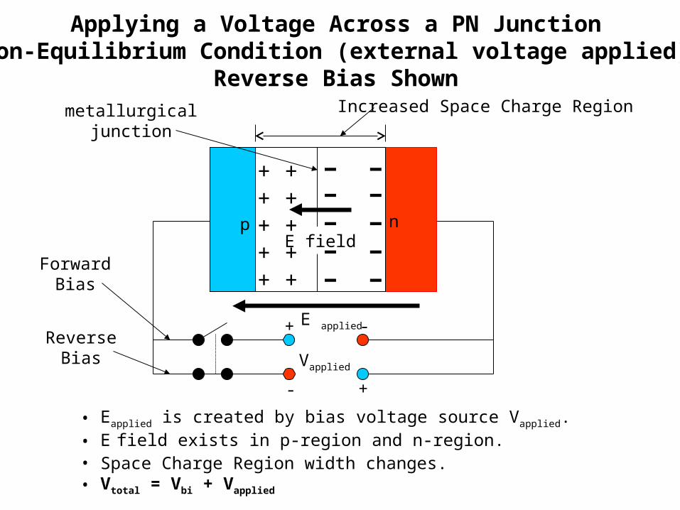
Applying a Voltage Across a PN JunctionNon-Equilibrium Condition (external voltage applied)
Reverse Bias Shown
• Eapplied is created by bias voltage source Vapplied.• E field exists in p-region and n-region.• Space Charge Region width changes.• Vtotal = Vbi + Vapplied
metallurgicaljunction
E field
Increased Space Charge Region
p n
E applied
Vapplied
-
+
+ ++ ++ ++ ++ +
- -- -- -- -- -
+
-
ForwardBias
ReverseBias

Reverse Bias PN JunctionNon-Equilibrium Condition (external voltage applied)
• ER is created by reverse bias voltage source VR.• ER is in same direction as internal E field.• Space Charge Region width increases.• Vtotal = Vbi + VR
• Ireverse is created from diffusion currents in the space charge region
metallurgicaljunction
E field
Increased Space Charge Region
p n
E R
VR
- +
+ ++ ++ ++ ++ +
- -- -- -- -- -
Ireverse

Conduction and Valance Band Diagram for PN JunctionReverse Bias Voltage Applied
Vtotal = Vbi + VR
- xp + xnx = 0
eVbi + eVR
Ec
Ev
p region n region
space charge region Ec
Ev

Forward Bias PN Junction (Diode)Non-Equilibrium Condition
• Eapplied is created by voltage source Va.• Eapplied must be greater than internal E field for IForwad to exist.• When Eapplied = E field, Va is called the “turn on” voltage.
metallurgicaljunction
E field
Space Charge Region
p n
E applied
Va
IForward
+ -
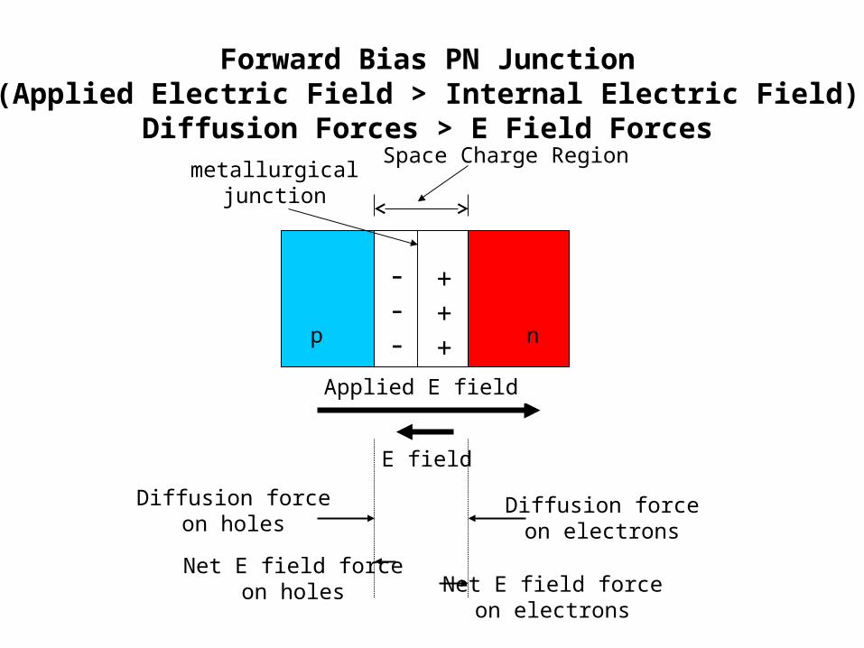
Forward Bias PN Junction(Applied Electric Field > Internal Electric Field)
Diffusion Forces > E Field Forcesmetallurgical
junction
E field
Space Charge Region
p n
+++
---
Diffusion forceon holes
Diffusion forceon electrons
Net E field forceon electrons
Net E field forceon holes
Applied E field
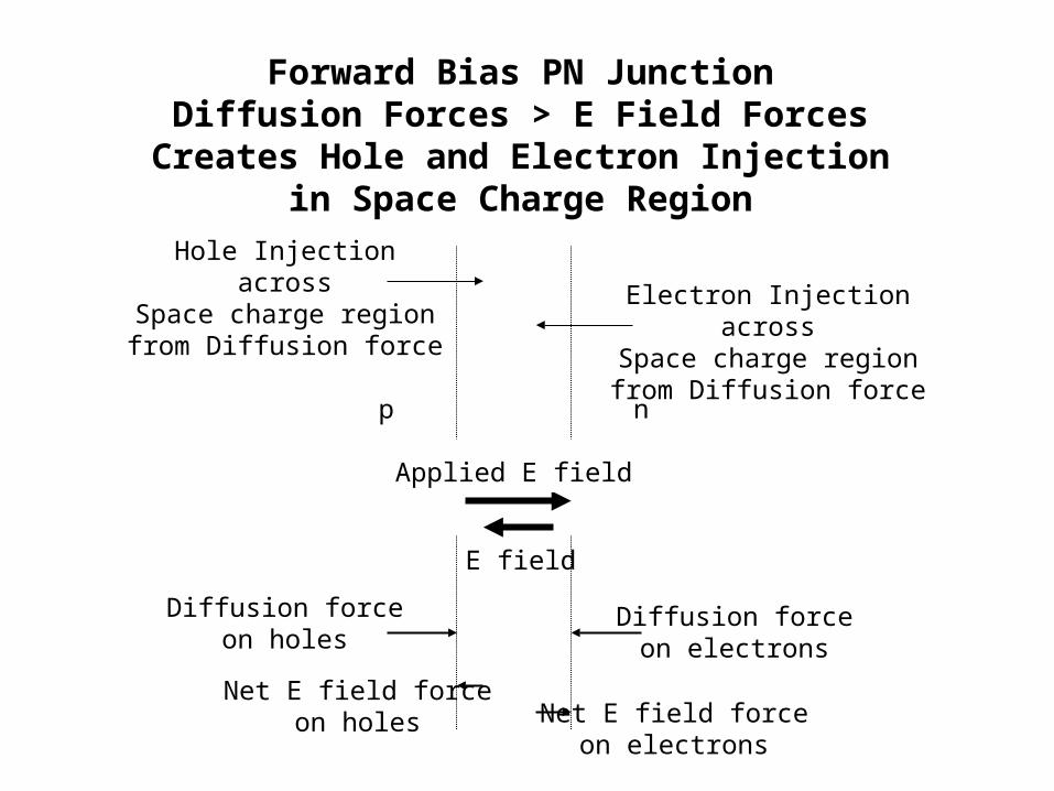
Forward Bias PN JunctionDiffusion Forces > E Field Forces
Creates Hole and Electron Injectionin Space Charge Region
E field
p
Diffusion forceon holes
Diffusion forceon electrons
Net E field forceon electrons
Net E field forceon holes
Applied E field
n
Hole Injectionacross
Space charge regionfrom Diffusion force
Electron Injectionacross
Space charge regionfrom Diffusion force

Forward Bias PN JunctionDiffusion Forces > E Field Forces
Creates Hole and Electron Injectionin Space Charge Region
p n
Hole Injectionacross
Space charge regionfrom Diffusion force
Jp|inj
Electron Injectionacross
Space charge regionfrom Diffusion force
Jn|inj
Currentdensity
Total Current density
Jtotal
Jtotal = Jp|inj + Jn|inj

Forward Bias PN JunctionElectron and Hole Current
Components
p n
hole diffusioncurrent
Jp|dif
electron diffusioncurrent
Jn|dif
Currentdensity
Total Current density
Jtotal
hole driftcurrent
Jp|drf
electron driftcurrent
Jn|drf
hole injectioncurrent
Jp|inj
electron injectioncurrent
Jn|inj

Forward Bias PN JunctionElectron and Hole Current
Components
p n
Jp|difJn|dif
Currentdensity
Jtotal
p-region: Jtotal = Jp|drf + Jn|dif
n-region: Jtotal = Jn|drf + Jp|dif
space charge region: Jtotal = Jn|inj + Jp|inj
Jp|drf Jn|drf
Jp|inj
Jn|inj

Ideal PN JunctionCurrent-Voltage Relationship
JS
Jtotal
JS = Reverse Bias Current DensityVa = Applied VoltageJtotal = JS[exp(eVa/(kT) - 1]
Va
turn on voltage

Key Concepts of PN Junction
• Thermal Equalibrium (no voltage source applied)• Internal E field created by diffusion currents• Built in potential, Vbi, exists• Space charge region created• E field is zero outside of space charge region• No current flow
• Forward Bias Applied• Hole and electron injection in space charge region• Total current density is constant through out semiconductor• Diffusion, injection, and drift currents exist• E field is not zero outside of space charge region
• Reverse Bias Applied• A constant reverse bias current exists for large applied voltages due to diffusion currents

PN Junction Hole and Electron InjectionReversible Process
Forward biased voltage applied to a PN junction creates hole and electron injection carriers within the space charge region.
External photon energy absorbed in space charge region creates holeand electron injection carriers that are swept out by the internalE field creating a voltage potential.

PN Junction Solar Cell OperationStep 1Photon
h > EgSpace Charge Region
+
+
+
+
+
E field
p n
e-e-e-e-e-
• Photons create hole-electron pairs in space charge region
• Created hole-electron pairs swepted out by internal E field

PN Junction Solar Cell OperationStep 2
• Created hole-electron pairs are swept out by the E field.• creates excess holes in p-region• creates excess electrons in n-region• Einjected is created by excess holes and electrons
• Photocurrent, IL, is in reverse bias direction
Photonh > Eg
Space Charge Region
E field
p nIL
E injected
+
+
+
+
+
e-e-e-e-e-
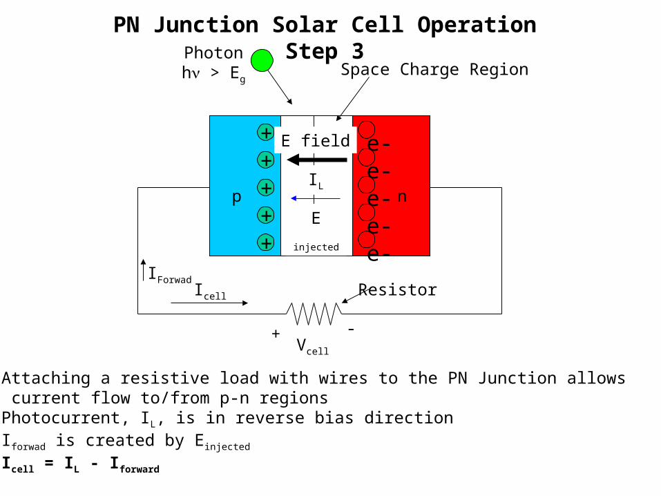
PN Junction Solar Cell OperationStep 3
• Attaching a resistive load with wires to the PN Junction allows current flow to/from p-n regions• Photocurrent, IL, is in reverse bias direction• Iforwad is created by Einjected
• Icell = IL - Iforward
Photonh > Eg
Space Charge Region
E field
p n
Resistor
Vcell
IL
Icell
IForwad
+ -
E injected
+
+
+
+
+
e-e-e-e-e-

PN Junction Solar Cell OperationStep 3
• Icell = IL - Iforward
• Icell = IL - IS[exp(eVcell/(kT) -1]• Icell is always in reverse bias direction
Photonh > Eg
Space Charge Region
E field
p n
Resistor
Vcell
IL
Icell
IForwad
+ -
E injected
+
+
+
+
+
e-e-e-e-e-
heat

Typical Silicon Solar Cell Design
N-typeSiliconWafer
P-typeDoping
Protective High Transmission Layer
To load
Wires
4-6 inches
0.6 mm
Photons
• Photons transmit through thin protective layer and thin P-type doped layer and create hole-electron pairs in space charge region• Typical Silicon Single Cell Voltage Output = ~ 0.5 volts

Silicon Solar Cell 6 Volt Panel Series-Parallel Design
12 cells in series = 6 volts
6 volts
p to n connection
-
+

External Factors Influencing Solar Cell Effeciency
• Photon transmission, reflection, and absorption of protective layer• Maximum transmission desired• Minimum reflection and absorption desired
• Polarization of protective layer• Minimum polarized transmission desired
• Photon Intensity• Increased intensity (more photons) increases cell current, Icell
• Cell voltage, Vcell, increases only slightly• Larger cell area produces larger current (more incident photons)
• Theoretical Silicon Solar Cell Maximum Efficiency = 28%• Typical Silicon Solar Cell Efficiency = 10-15%


