34
MicroLab, vlsi27 (1/34) JMM v1.0 Analog Microelectronics Basic OpAmp Design and Compensation Today’s handouts: (1) Lecture Slides
| Date post: | 08-Apr-2016 |
| Category: |
Documents |
| Upload: | ammar-ajmal |
| View: | 21 times |
| Download: | 0 times |
MicroLab, vlsi27 (1/34)
JMM v1.0
Analog MicroelectronicsBasic OpAmp Design and Compensation
Today’s handouts:(1) Lecture Slides
MicroLab, vlsi27 (2/34)
JMM v1.0
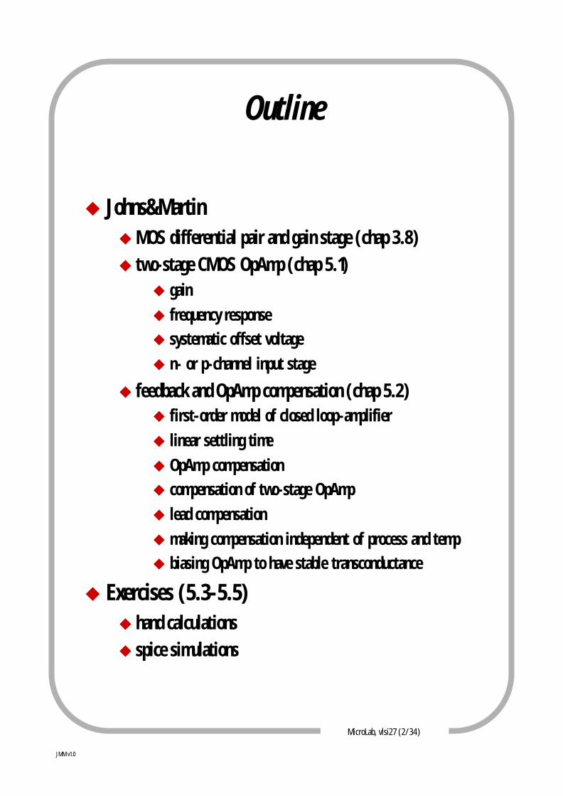
Outline
u Johns&MartinuMOS differential pair and gain stage (chap 3.8)u two-stage CMOS OpAmp (chap 5.1)
u gainu frequency responseu systematic offset voltageu n- or p-channel input stage
u feedback and OpAmp compensation (chap 5.2)u first-order model of closed loop-amplifieru linear settling timeu OpAmp compensationu compensation of two-stage OpAmpu lead compensationu making compensation independent of process and tempu biasing OpAmp to have stable transconductance
u Exercises (5.3-5.5)u hand calculationsu spice simulations
MicroLab, vlsi27 (3/34)
JMM v1.0
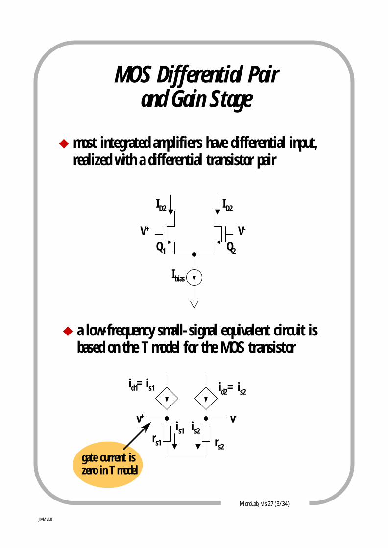
MOS Differential Pair and Gain Stage
u most integrated amplifiers have differential input, realized with a differential transistor pair
Ibias
Q1 Q2
V+
ID2
V-
ID2
u a low-frequency small-signal equivalent circuit is based on the T model for the MOS transistor
rs1
v+is2
v-
id2=is2
rs2
id1=is1
is1
gate current is zero in T model
MicroLab, vlsi27 (4/34)
JMM v1.0
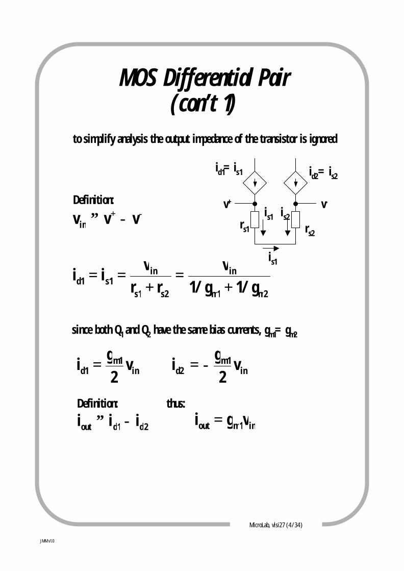
MOS Differential Pair (con’t 1)
to simplify analysis the output impedance of the transistor is ignored
−+ −≡ vvv in
Definition:
2m1m
in
2s1s
in1s1d g/1g/1
vrr
vii+
=+
==
since both Q1 and Q2 have the same bias currents, gm1=gm2
in1m
1d v2
gi =
rs1
v+is2
v-
id2=is2
rs2
id1=is1
is1
is1
in1m
2d v2
gi −=
2d1dout iii −≡Definition:
in1mout vgi =thus:
MicroLab, vlsi27 (5/34)
JMM v1.0
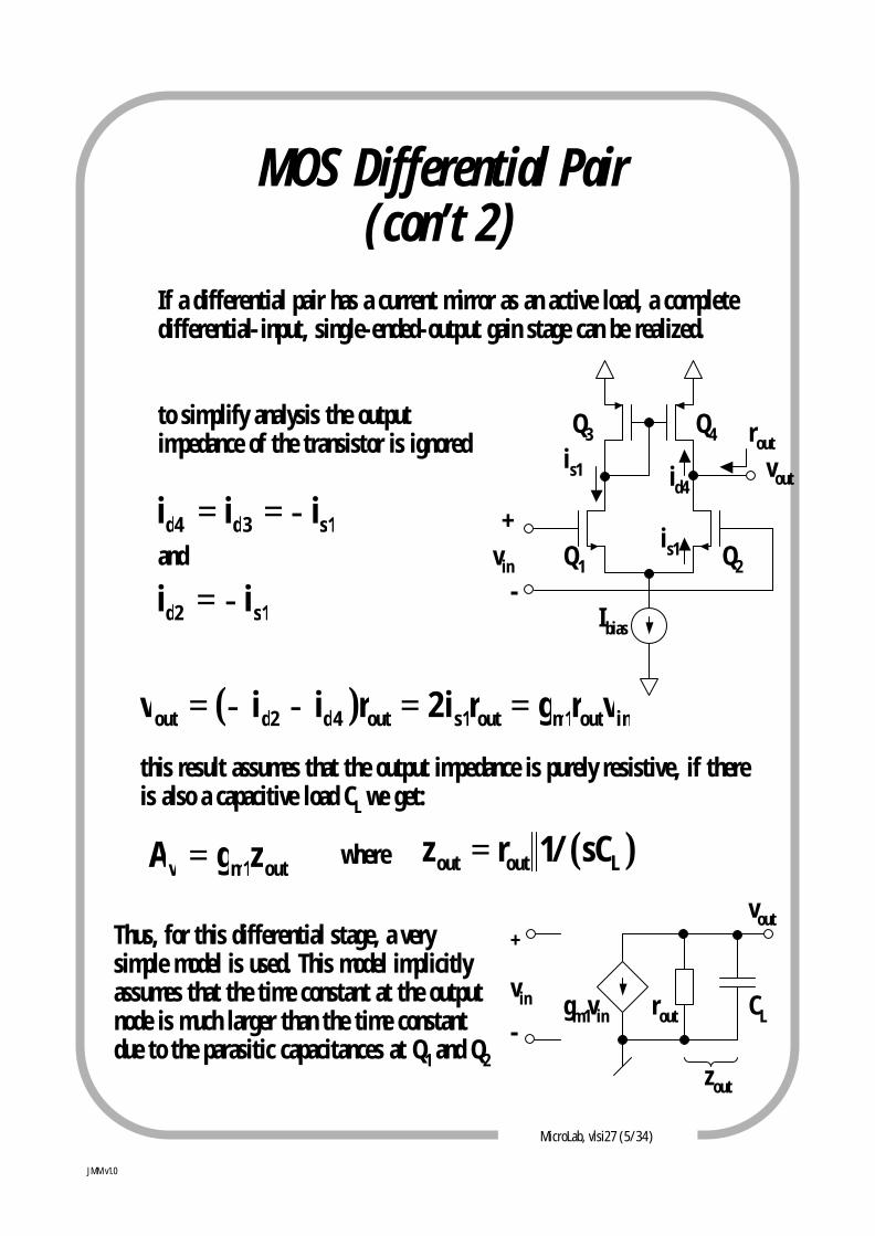
MOS Differential Pair (con’t 2)
If a differential pair has a current mirror as an active load, a completedifferential-input, single-ended-output gain stage can be realized.
Ibias
Q1 Q2vin
id4is1
Q4 routQ3
vout
is1+
-
to simplify analysis the output impedance of the transistor is ignored
1s3d4d iii −==
1s2d ii −=and
( ) inout1mout1sout4d2dout vrgri2riiv ==−−=
this result assumes that the output impedance is purely resistive, if thereis also a capacitive load CL we get:
out1mv zgA = ( )Loutout sC/1rz =where
Thus, for this differential stage, a very simple model is used. This model implicitlyassumes that the time constant at the outputnode is much larger than the time constantdue to the parasitic capacitances at Q1 and Q2
vout
vin
+
-gm1vin rout CL
zout

MicroLab, vlsi27 (6/34)
JMM v1.0
MOS Differential Pair (con’t 3)
The evaluation of the output resistance rout is determined by using thesmall-signal equivalent circuit and applying a voltage at the output node.Note that the T-model is used for Q1, Q2 and Q3, and the the hybrid-πmodel is used for Q4.
Ibias
Q1 Q2vin
id4is1
Q4 routQ3
vout
is1+
-
x
xout i
vr ≡
( )4ds2ds1mv rrgA =
4ds2dsout rrr =
rs1
is1
is1 rds1 rs2
is2
is2rds2
vx +-
is5 ix1 ix4 ix
ix3ix2
rds4rds3//rs3
gm4vava
+
-
MicroLab, vlsi27 (7/34)
JMM v1.0
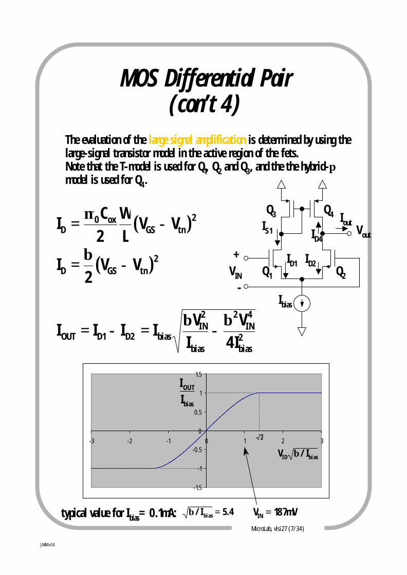
MOS Differential Pair (con’t 4)
The evaluation of the large signal amplification is determined by using thelarge-signal transistor model in the active region of the fets.Note that the T-model is used for Q1, Q2 and Q3, and the the hybrid-πmodel is used for Q4.
( )2tnGS
ox0D VV
LW
2CI −
µ=
Ibias
Q1 Q2VIN
ID4IS1
Q4 IoutQ3
Vout
ID2+
-
ID1
2bias
4IN
2
bias
2IN
bias2D1DOUT I4V
IVIIII β
−β
=−=
( )2tnGSD VV
2I −
β=
-1.5
-1
-0.5
0
0.5
1
1.5
-3 -2 -1 0 1 2 3
bias
OUT
II
2
b i a sI D I/V β
4.5I/ b i a s =βtypical value for Ibias=0.1mA: mV187VIN =

MicroLab, vlsi27 (8/34)
JMM v1.0
Two-Stage CMOS OpAmp
u Basic OpAmp design are discussedu OpAmp gainu frequency responseu slew rateu systematic offset voltageu n-channel or p-channel input stage
-A2 1A1-
+
CC
Vin Vout
second gain stage
differentialinput stage
outputbuffer
singleended output e.x. common-source
gain stage withactive load
capacitor ensures stability when OpAmp
is used in feedbackCC is often calledMiller capacitanceto illustrate itseffect on input
output gain stage only present when resistive loads need to be driven
MicroLab, vlsi27 (9/34)
JMM v1.0
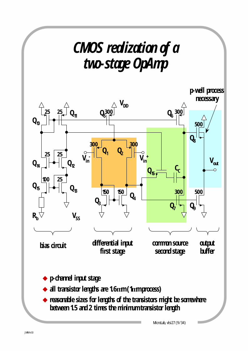
CMOS realization of a two-stage OpAmp
bias circuit differential inputfirst stage
common sourcesecond stage
outputbuffer
u p-channel input stageu all transistor lengths are 1.6µm (1µm process)u reasonable sizes for lengths of the transistors might be somewhere
between 1.5 and 2 times the minimum transistor length
p-well processnecessary
Q1 Q2Vin
-
Q4Q3
Vin+
Q15 Q13
Q12Q14
Q10
Q11 Q525 25
25 25
100 25
300
300 300
150 150
Rb
Q7
300 500
Q6
Q8
300
Q9
Q16CC
Vout
VDD
VSS
500
MicroLab, vlsi27 (10/34)
JMM v1.0
Two-Stage OpAmpGain
u overall gain for low frequency application is the most critical parameter of an OpAmp
( )4111 dsdsmv rrgA =
222
11
11
biasoxpDoxpm
IL
WCI
LW
Cg
=
= µµ
tiDGiDi
idsi VV
IL
r +≅ α
gain of the first stage(differential stage)
approximation to the finite outputresistance, where a is technology dependent parameter: 5e-6 V1/2/mignoring short channel effects
gain of the second stage(common-source stage)
( )7672 dsdsmv rrgA −=
989
93
dsdsmL
mv gggG
gA
+++=gain of the third stage
(common-drain stage)
9889
93
dsdssmL
mv ggggG
gA
++++=gain of the third stage
with body effect (bulknot connected to source)
FSB
ms V
gg
φγ
22 +=body effect constant γ=0.5V1/2
2φF=0.7V
MicroLab, vlsi27 (11/34)
JMM v1.0
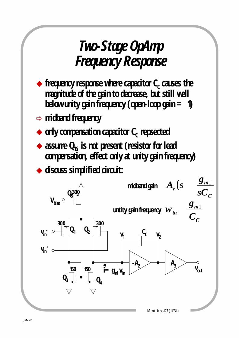
Two-Stage OpAmpFrequency Response
u frequency response where capacitor Cc causes the magnitude of the gain to decrease, but still well below unity gain frequency (open-loop gain = 1)
ð midband frequencyu only compensation capacitor CC repsectedu assume Q16 is not present (resistor for lead
compensation, effect only at unity gain frequency)u discuss simplified circuit:
Q1 Q2vin-
Q4Q3
vin+
Q5300
300 300
150 150
Vbias
CC
-A2 A3 vout
v1 v2
i=gm1 vin
( )C
mv sC
gsA 1≅
C
mta C
g 1≅ω
midband gain
untity gain frequency
MicroLab, vlsi27 (12/34)
JMM v1.0
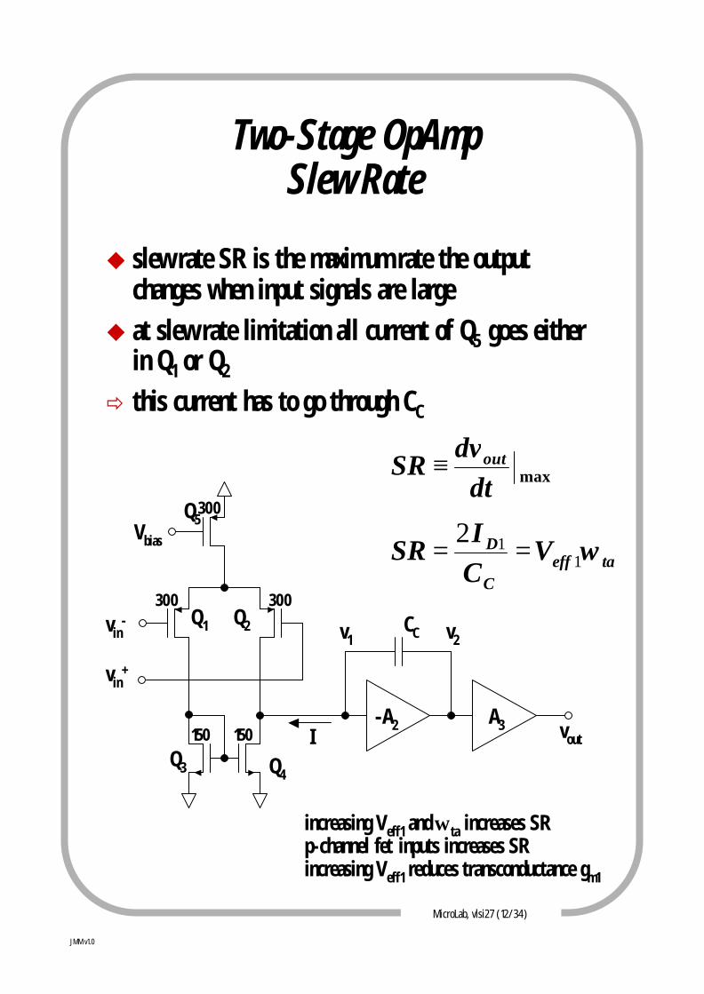
Two-Stage OpAmpSlew Rate
u slew rate SR is the maximum rate the output changes when input signals are large
u at slew rate limitation all current of Q5 goes either in Q1 or Q2
ð this current has to go through CC
maxdtdv
SR out≡
taeffC
D VCI
SR ω112
==
increasing Veff1 and ω ta increases SRp-channel fet inputs increases SRincreasing Veff1 reduces transconductance gm1
Q1 Q2vin-
Q4Q3
vin+
Q5300
300 300
150 150
Vbias
CC
-A2 A3 vout
v1 v2
I
MicroLab, vlsi27 (13/34)
JMM v1.0
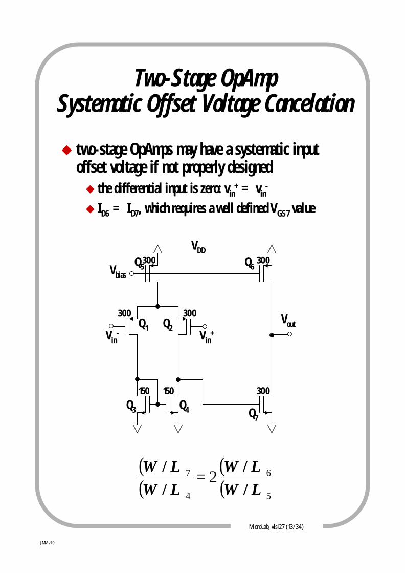
Two-Stage OpAmpSystematic Offset Voltage Cancelation
u two-stage OpAmps may have a systematic input offset voltage if not properly designedu the differential input is zero: vin
+= vin-
u ID6 = ID7, which requires a well defined VGS7 value
( )( )
( )( )5
6
4
7 2LWLW
LWLW
//
//
=
Q1 Q2Vin
-
Q4Q3
Vin+
Q5300
300 300
150 150
Q7
300
Q6300
Vout
VDD
Vbias
MicroLab, vlsi27 (14/34)
JMM v1.0
Two-Stage OpAmpn- or p- channel input stage
u comparison between n- and p-channel input stage OpAmpsu overal dc gain is largely unaffected since both designs
have one stage with n-channel and one stage with one or more p-channel driving fets.
u for a given power dissipation, and therefore bias current, having a p-channel input-pair stage maximizes the slew rate.
u having a p-channel input first stage implies that the second stage has an n-channel input drive fet. This arrangement maximizes the transconductance of the drive fet of teh 2nd stage, which is critical when high frequency operation is important.
u output stage: n-channel source follower is preferable because this will have less of a voltage drop (if separate p-well is used). Its higher transconductance reduces the effect of the load cap on the second pole. There is also less degradation on the gain when small load resistances are being driven.
ð p-channel input fets for the first stage is almost always the best choice
MicroLab, vlsi27 (15/34)
JMM v1.0
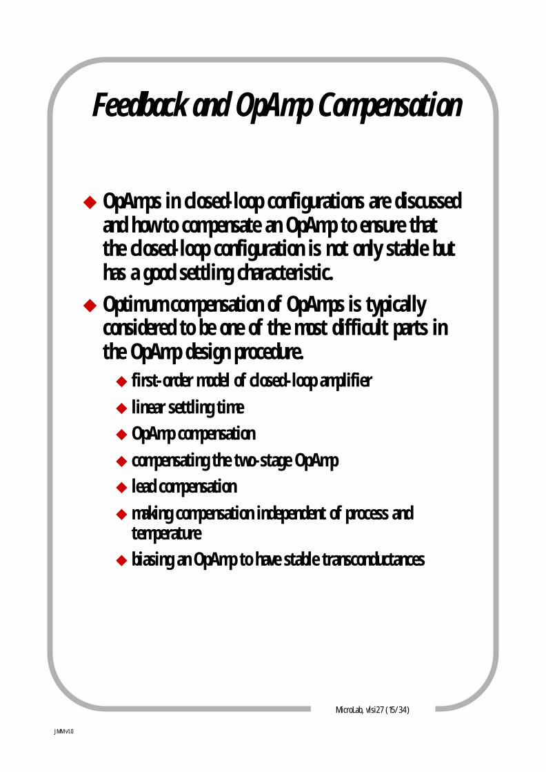
Feedback and OpAmp Compensation
u OpAmps in closed-loop configurations are discussed and how to compensate an OpAmp to ensure that the closed-loop configuration is not only stable but has a good settling characteristic.
u Optimum compensation of OpAmps is typically considered to be one of the most difficult parts in the OpAmp design procedure.u first-order model of closed-loop amplifieru linear settling timeu OpAmp compensationu compensating the two-stage OpAmpu lead compensationumaking compensation independent of process and
temperatureu biasing an OpAmp to have stable transconductances
MicroLab, vlsi27 (16/34)
JMM v1.0
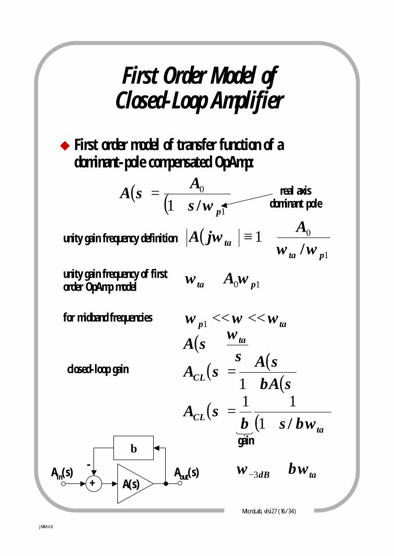
First Order Model of Closed-Loop Amplifier
u First order model of transfer function of a dominant-pole compensated OpAmp:
( ) ( )1
0
1 psA
sAω/+
= real axisdominant pole
( )1
01pta
taA
jAωω
ω/
≅≡
10 pta A ωω ≅
( )s
sA taω≅
+ A(s)
β-
Ain(s) Aout(s)
( ) ( )( )sA
sAsACL β+
=1
( ) ( )taCL s
sAβωβ /+
=1
11
gain
unity gain frequency definition
unity gain frequency of first order OpAmp model
for midband frequencies tap ωωω <<<<1
closed-loop gain
tadB βωω ≅−3
MicroLab, vlsi27 (17/34)
JMM v1.0
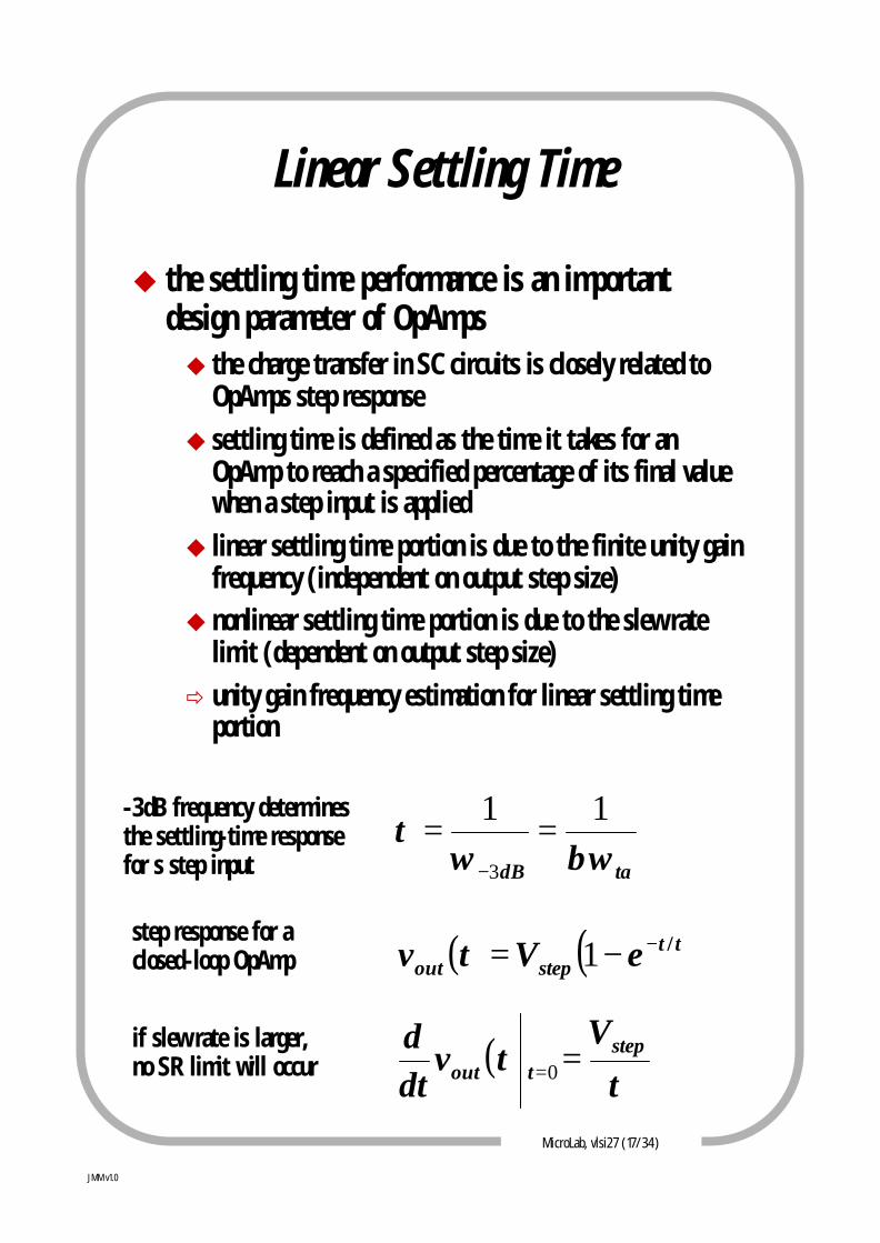
Linear Settling Time
u the settling time performance is an important design parameter of OpAmpsu the charge transfer in SC circuits is closely related to
OpAmps step responseu settling time is defined as the time it takes for an
OpAmp to reach a specified percentage of its final value when a step input is applied
u linear settling time portion is due to the finite unity gain frequency (independent on output step size)
u nonlinear settling time portion is due to the slew rate limit (dependent on output step size)
ð unity gain frequency estimation for linear settling time portion
( ) ( )τ/tstepout eVtv −−= 1
tadB βωωτ
11
3
==−
( )τstep
tout
Vtv
dtd
==0
-3dB frequency determines the settling-time response for s step input
step response for a closed-loop OpAmp
if slew rate is larger,no SR limit will occur
MicroLab, vlsi27 (18/34)
JMM v1.0
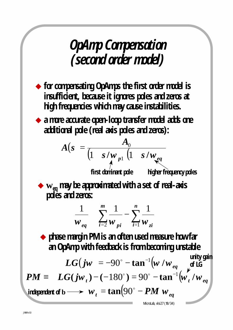
OpAmp Compensation(second order model)
u for compensating OpAmps the first order model is insufficient, because it ignores poles and zeros at high frequencies which may cause instabilities.
u a more accurate open-loop transfer model adds one additional pole (real axis poles and zeros):
( ) ( )( )eqp ssA
sAωω // ++
=11 1
0
first dominant pole higher frequency poles
uωeq may be approximated with a set of real-axis poles and zeros:
∑∑==
−≅n
i zi
m
i pieq 12
111ωωω
u phase margin PM is an often used measure how far an OpAmp with feedback is from becoming unstable
( )eqttjLGPM ωωω /tan)()( 190180 −−=−−∠≡ oo
( ) eqt PM ωω −= o90tan
( ) ( )eqjLG ωωω /tan 190 −−−=∠ o
independent of β
unity gain of LG
MicroLab, vlsi27 (19/34)
JMM v1.0
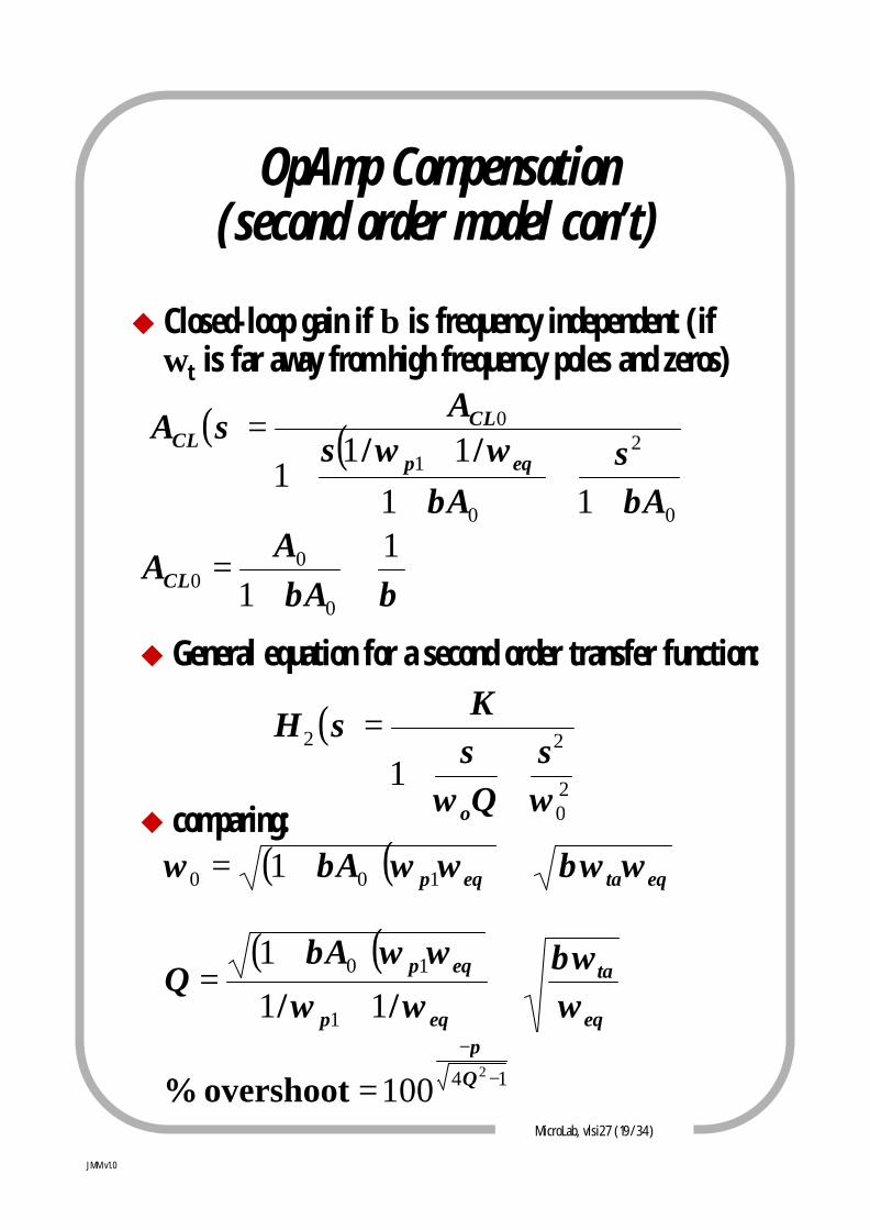
OpAmp Compensation(second order model con’t)
u Closed-loop gain if β is frequency independent (if ωt is far away from high frequency poles and zeros)
( ) ( )0
2
0
1
0
1111
1A
sA
sA
sAeqp
CLCL
ββωω
++
++
+=
//
ββ1
1 0
00 ≅
+=
AA
ACL
u General equation for a second order transfer function:
( )20
22
1ωωs
QsK
sH
o
++=
u comparing:( )( ) eqtaeqpA ωβωωωβω ≅+= 100 1
( )( )eq
ta
eqp
eqpAQ
ωβω
ωω
ωωβ≅
+
+=
// 11
1
1
10
14 2
100 −
−
= Q
π
overshoot %
MicroLab, vlsi27 (20/34)
JMM v1.0
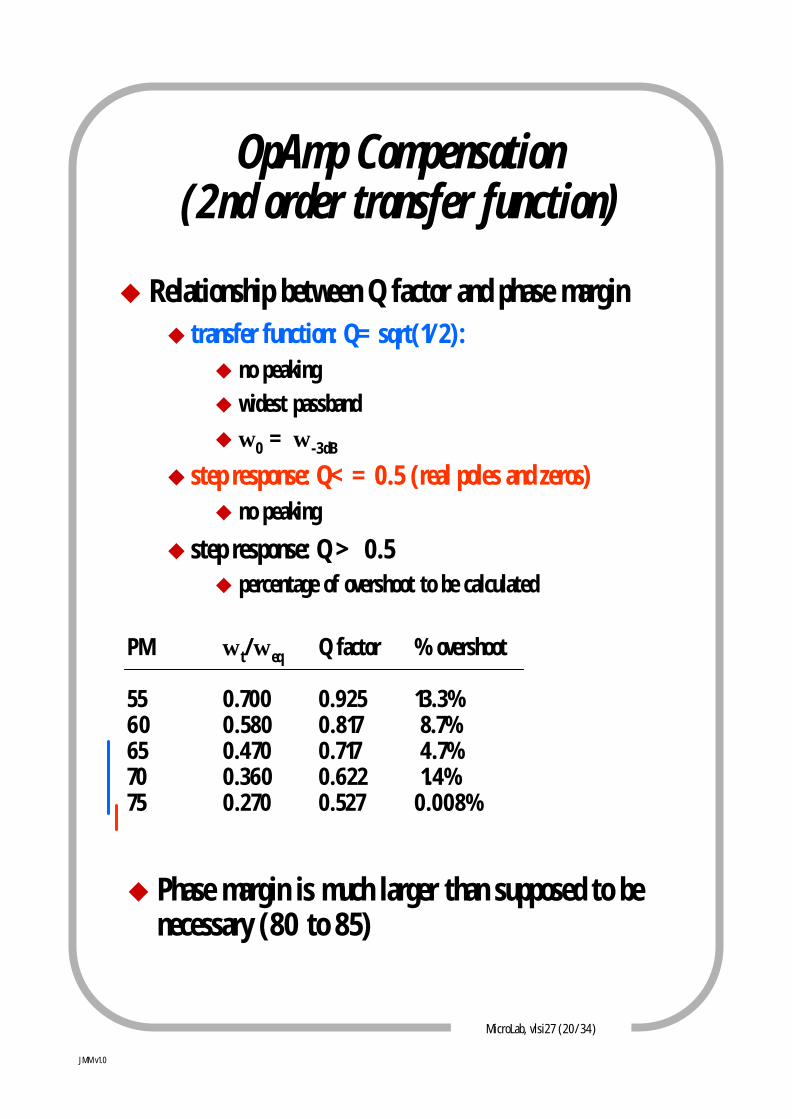
OpAmp Compensation(2nd order transfer function)
u Relationship between Q factor and phase marginu transfer function: Q=sqrt(1/2):
u no peakingu widest passbandu ω0 = ω-3dB
u step response: Q<=0.5 (real poles and zeros)u no peaking
u step response: Q > 0.5u percentage of overshoot to be calculated
PM ω t/ωeq Q factor % overshoot
55 0.700 0.925 13.3%60 0.580 0.817 8.7%65 0.470 0.717 4.7%70 0.360 0.622 1.4%75 0.270 0.527 0.008%
u Phase margin is much larger than supposed to be necessary (80 to 85)
MicroLab, vlsi27 (21/34)
JMM v1.0
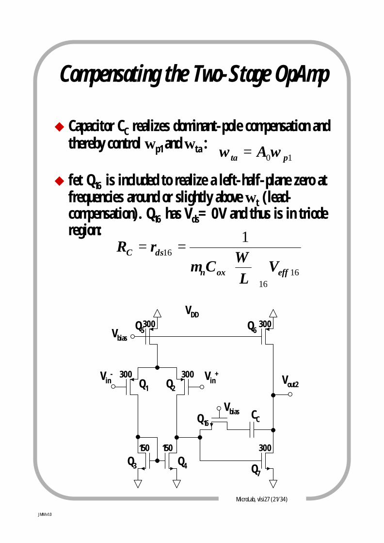
Compensating the Two-Stage OpAmp
u Capacitor CC realizes dominant-pole compensation and thereby control ωp1 and ωta :
u fet Q16 is included to realize a left-half-plane zero at frequencies around or slightly above ωt (lead-compensation). Q16 has Vds=0V and thus is in triode region:
Q1 Q2Vin
-
Q4Q3
Vin+
Q5300
300 300
150 150
Q7
300
Q6300
Vout2
VDD
Vbias
Q16
Vbias CC
10 pta A ωω =
1616
161
effoxn
dsC
VL
WCrR
==µ
MicroLab, vlsi27 (22/34)
JMM v1.0
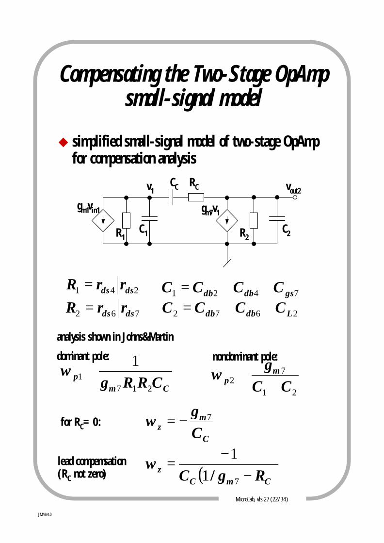
Compensating the Two-Stage OpAmpsmall-signal model
u simplified small-signal model of two-stage OpAmp for compensation analysis
gm7v1
R1C2R2
C1
CCv1
gm1vin1
RC vout2
241 dsds rrR =
762 dsds rrR =7421 gsdbdb CCCC ++=
2672 Ldbdb CCCC ++=
Cmp CRRg 2171
1≅ω
21
72 CC
gmp +
≅ω
C
mz C
g 7−=ω
( )CmCz RgC −
−=
711
/ω
analysis shown in Johns&Martin
dominant pole: nondominant pole:
for RC=0:
lead compemsation(RC not zero)
MicroLab, vlsi27 (23/34)
JMM v1.0
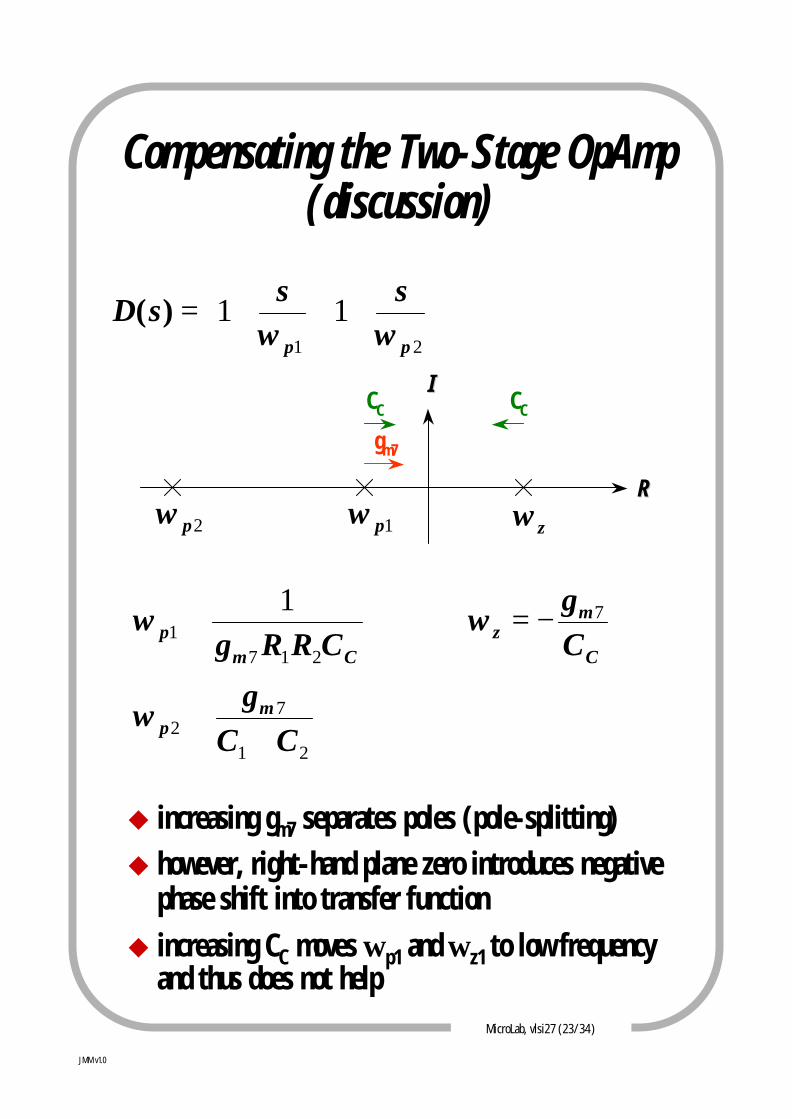
Compensating the Two-Stage OpAmp(discussion)
u increasing gm7 separates poles (pole-splitting)u however, right-hand plane zero introduces negative
phase shift into transfer functionu increasing CC moves ωp1 and ωz1 to low frequency
and thus does not help
RR
II
1pω2pω zω
gm7
CCCC
+
+=
21
11pp
sssD
ωω)(
Cmp CRRg 2171
1≅ω
21
72 CC
gmp +
≅ω
C
mz C
g 7−=ω

MicroLab, vlsi27 (24/34)
JMM v1.0
Compensating the Two-Stage OpAmp(lead compensation)
u with a non-zero RC, a third pole is introduced, but is at high frequency and has almost no effect
u However the zero opens a number of possibilities:
u one could eliminate the right-half plane zero:
u one could choose RC to be even larger and thus move the right-half-plane zero into the left half plane to cancel the nondominant pole ωp2:
u one could choose RC even larger to move the now left-half-plane zero to a frequency slightly greater than the unity-gain frequency that would result without the resistor - say 20% larger (recommended):
( )CmCz RgC −
−=
711
/ω
71 mC gR /=
++=
CmC C
CCg
R 21
7
11
1211
mC g
R.
≅tz ωω 21.=
MicroLab, vlsi27 (25/34)
JMM v1.0
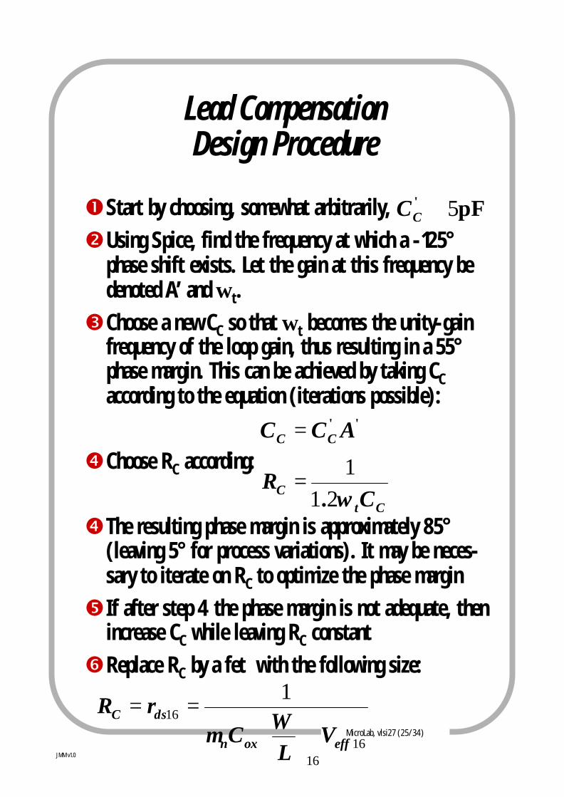
Lead CompensationDesign Procedure
Start by choosing, somewhat arbitrarily,Using Spice, find the frequency at which a -125°
phase shift exists. Let the gain at this frequency be denoted A’ and ωt.Choose a new CC so that ωt becomes the unity-gain
frequency of the loop gain, thus resulting in a 55° phase margin. This can be achieved by taking CCaccording to the equation (iterations possible):
Choose RC according:
The resulting phase margin is approximately 85° (leaving 5° for process variations). It may be neces-sary to iterate on RC to optimize the phase marginIf after step 4 the phase margin is not adequate, then
increase CC while leaving RC constantReplace RC by a fet with the following size:
pF' 5≅CC
'' ACC CC =
CtC C
Rω211
.=
1616
161
effoxn
dsC
VL
WCrR
==µ
MicroLab, vlsi27 (26/34)
JMM v1.0
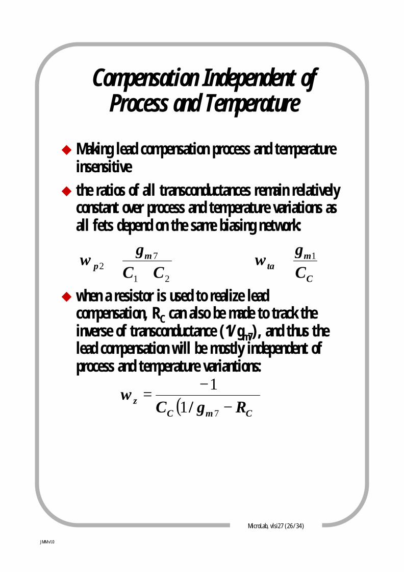
Compensation Independent of Process and Temperature
u Making lead compensation process and temperature insensitive
u the ratios of all transconductances remain relatively constant over process and temperature variations as all fets depend on the same biasing network:
u when a resistor is used to realize lead compensation, RC can also be made to track the inverse of transconductance (1/gm7), and thus the lead compensation will be mostly independent of process and temperature variantions:
( )CmCz RgC −
−=
711
/ω
21
72 CC
gmp +
≅ωC
mta C
g 1≅ω
MicroLab, vlsi27 (27/34)
JMM v1.0
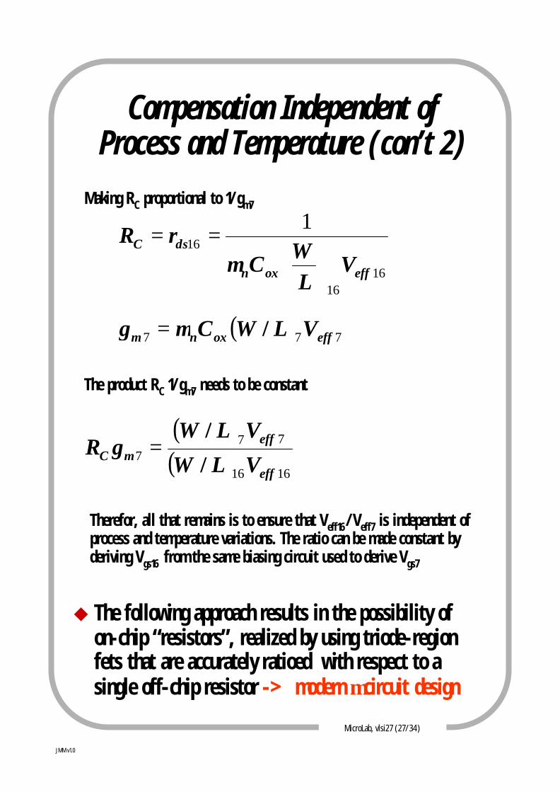
Compensation Independent of Process and Temperature (con’t 2)
1616
161
effoxn
dsC
VL
WCrR
==µ
( ) 777 effoxnm VLWCg /µ=
Making RC proportional to 1/gm7
The product RC 1/gm7 needs to be constant
( )( ) 1616
777
eff
effmC VLW
VLWgR
/
/=
Therefor, all that remains is to ensure that Veff16/Veff7 is independent of process and temperature variations. The ratio can be made constant by deriving Vgs16 from the same biasing circuit used to derive Vgs7
u The following approach results in the possibility of on-chip “resistors”, realized by using triode-region fets that are accurately ratioed with respect to a single off-chip resistor -> modern µcircuit design
MicroLab, vlsi27 (28/34)
JMM v1.0
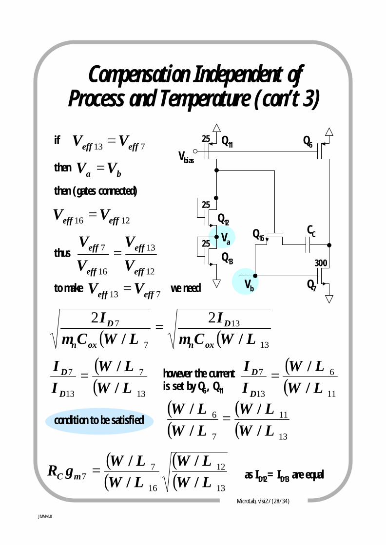
Compensation Independent of Process and Temperature (con’t 3)
if
Q7
300
Q6
Q16
Vb
CC
Q13
Q12
Q1125
25
25
Vbias
Va
713 effeff VV =
then ba VV =then (gates connected)
1216 effeff VV =
thus12
13
16
7
eff
eff
eff
eff
V
V
V
V=
to make 713 effeff VV = we need
( ) ( )13
13
7
7 22LWC
ILWC
I
oxn
D
oxn
D
// µµ=
( )( )13
7
13
7
LWLW
II
D
D
//
= however the current is set by Q6, Q11
( )( )11
6
13
7
LWLW
II
D
D
//
=
( )( )
( )( )13
11
7
6
LWLW
LWLW
//
//
=
as ID12=ID13 are equal ( )( )
( )( )13
12
16
77 LW
LWLWLW
gR mC //
//
=
condition to be satisfied
MicroLab, vlsi27 (29/34)
JMM v1.0
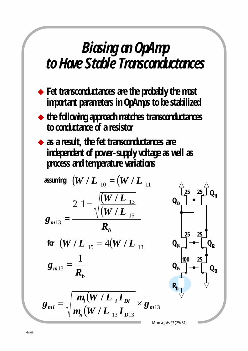
Biasing an OpAmp to Have Stable Transconductances
u Fet transconductances are the probably the most important parameters in OpAmps to be stabilized
u the following approach matches transconductances to conductance of a resistor
u as a result, the fet transconductances are independent of power-supply voltage as well as process and temperature variations
Q15 Q13
Q12Q14
Q10
Q1125 25
25 25
100 25
Rb
( ) ( )1110 LWLW // =assuming
( )( )
bm R
LWLW
g
−
= 15
13
13
12//
( ) ( )1315 4 LWLW // =for
bm R
g1
13 =
( )( ) 13
1313m
Dn
Diiimi g
ILWILW
g ×=//
µµ
MicroLab, vlsi27 (30/34)
JMM v1.0
Exercises VLSI-27
Ex ana3.9 (difficulty: easy): Consider a differential pair amplifier shown on transparency vlsi-27/3 where Ibias=200µA and all transistors have W=100µm and L=1.6µm. GivenµnCox=92µA/V2 and rds-n=8000 [L (µm)]/[ID (mA)]. Find the output impedance and the gain.
Result: Av =68.6V/V, rout=64kΩ (see Johns/Martin pp146)
Ex ana5.1 (difficulty: easy): Find the gain of theOpAmp shown on transparency vlsi-27/9. Assume ID5=100µA, first stage VDG=0.5V, 2nd and 3rd stage VDG=1V and bulk of Q8 connected to VSS. Given µnCox =3µpCox=96µA/V2, VDD=-VSS=2.5V, RL=10kΩ, γ=0.5V1/2, φF=0.35V, α=5e6V1/2/m, Vtn=- Vtn=0.8V.
Result: Av =-6092V/V (see Johns/Martin pp224)
MicroLab, vlsi27 (31/34)
JMM v1.0
Exercises VLSI-27 (con’t 2)
Ex ana5.2 (difficulty: easy): Find the unity gain frequency of the OpAmp shown on transparency vlsi-27/9, with CC=5pF . Assume ID5=100µA, first stage VDG=0.5V, 2nd and 3rd stage VDG=1V and bulk of Q8 connected to VSS. Given µnCox=3µpCox=96µA/V2, VDD=-VSS=2.5V, RL=10kΩ, γ=0.5V1/2, φF=0.35V, α=5e6V1/2/m, Vtn=- Vtn=0.8V.
Result: fta = 24.7MHz (see Johns/Martin pp227)
Ex ana5.3 (difficulty: easy): Find the slew rate of OpAmp on transparency vlsi-27/9, with CC=5pF . Assume ID5=100µA. What circuit chane could be done to double the slew rate but to keep ωta and bias currents unchanged?
Result: SR = 20V/µs, to double SR: CC=2.5pF and W1= W2= 75µm (see Johns/Martin pp229)
MicroLab, vlsi27 (32/34)
JMM v1.0
Exercises VLSI-27 (con’t 3)
Ex ana5.4 (difficulty: easy): Consider the OpAmpshown on transparency vlsi-27/9, where Q3 qnd Q4are each changed to widths of 120µm and we want the output stage have a bias current of 150µA. Find the new sizes of Q6 qnd Q7 such that there is no systematic offset voltage.
Result: W6 = 450µm, W7 = 360µm(see Johns/Martin pp231)
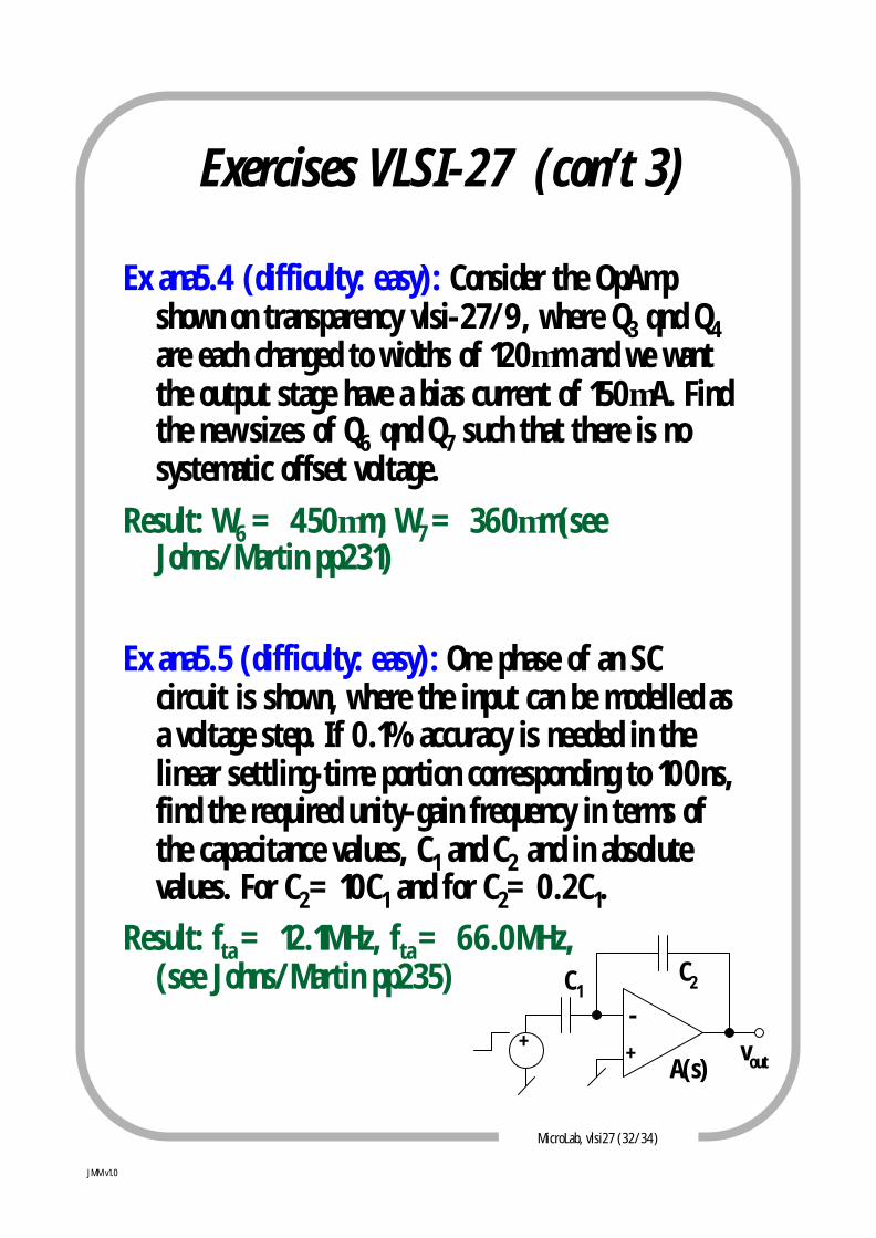
Ex ana5.5 (difficulty: easy): One phase of an SC circuit is shown, where the input can be modelled as a voltage step. If 0.1% accuracy is needed in the linear settling-time portion corresponding to 100ns, find the required unity-gain frequency in terms of the capacitance values, C1 and C2 and in absolute values. For C2=10C1 and for C2=0.2C1.
Result: fta = 12.1MHz, fta = 66.0MHz, (see Johns/Martin pp235)
+
-+
C1C2
voutA(s)

MicroLab, vlsi27 (33/34)
JMM v1.0
Exercises VLSI-27 (con’t 4)
Ex ana5.7 (difficulty: medium): OpAmp has an open-loop transfer function given by:
Assume that ω2=2π 50MHz and A0=104
a) Assuming ωz=inf, find ωp1 and the unity-gain frequency ωt‘ so that the OpAmp has a unity-gain phase margin of 55°
b) Assuming ωz=1.2 ωt‘ (use ωt‘ from a), what is the unity-gain frequency ωt. Also find the new phase margin.
Result: a) ωt‘=2π 35MHz, ωp1=2π 4.27kHz, b) ωt=2π 46.6MHz, PM= -85° (see Johns/Martin pp245)
( ) ( )( )( )21
0
111
ωωω
///
sssA
sAp
z
+++
=

MicroLab, vlsi27 (34/34)
JMM v1.0
Coming Up...
u Next topic… Advanced Current Mirrors and OpAmps
u Readings for next time… Johns&Martin: Sections 3.8 and 5
u Exercises: Have a look at the exercises in Johns&Martin.


