+ All Categories
Home > Documents > BasicFabricationSteps andLayout - Sharif

BasicFabricationSteps andLayout - Sharif

Date post: 11-Dec-2021
Category:
Upload: others
View: 2 times
Download: 0 times
Share this document with a friend
35
Basic Fabrication Steps and Layout and Layout Somayyeh Koohi Department of Computer Engineering Sharif University of Technology Adapted with modifications from lecture notes prepared by author
Transcript

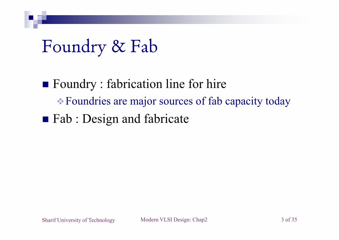
Basic Fabrication Stepsand Layoutand Layout

Somayyeh KoohiDepartment of Computer Engineering

Sharif University of TechnologyAdapted with modifications from lecture notes prepared by

author

Outline

� Fabrication steps� Transistor structures� Transistor behavior

Modern VLSI Design: Chap2 2 of 35Sharif University of Technology

� Transistor behavior�NMOS�PMOS

� Latch up

Foundry & Fab

� Foundry : fabrication line for hire�Foundries are major sources of fab capacity today

� Fab : Design and fabricate

Modern VLSI Design: Chap2 3 of 35Sharif University of Technology

� Fab : Design and fabricate

Silicon Lattice

� Semiconductor� Conductivity changed by adding

impurities� Impurities, called dopants, create

either n-type or p-type regions Si SiSi

Si SiSi

Modern VLSI Design: Chap2 4 of 35Sharif University of Technology

either n type or p type regions

� Transistors are built on asilicon substrate

� Silicon is a Group IV material� Forms crystal lattice with bonds

to four neighbors

Si SiSi

Si SiSi

Dopants

� Silicon is a semiconductor� Pure silicon has no free carriers and conducts poorly� Adding dopants increases the conductivity

� Gro p V (A i Ph h ): e tra electron (n t pe)

Modern VLSI Design: Chap2 5 of 35Sharif University of Technology

� Group V (Arsenic, Phosphorus): extra electron (n-type)� Group III (Boron): missing electron, called hole (p-type)

As SiSi

Si SiSi

Si SiSi

B SiSi

Si SiSi

Si SiSi

-

+

+

-

p-n Junctions

� A junction between p-type and n-typesemiconductor forms a diode

� Current flows only in one direction

Modern VLSI Design: Chap2 6 of 35Sharif University of Technology

� Current flows only in one direction

N-Diff P-Diff

anodecathode

Fabrication processes

� IC built on silicon substrate:� some structures diffused into substrate� other structures built on top of substrate

Modern VLSI Design: Chap2 7 of 35Sharif University of Technology

� Substrate regions are doped with n-type and p-typeimpurities� (n+ = heavily doped)

� Wires made of polycrystalline silicon (poly), multiplelayers of aluminum (metal)

� Silicon dioxide (SiO2) is insulator

Simple cross section

SiO2

metal2

metal3

Modern VLSI Design: Chap2 8 of 35Sharif University of Technology

substraten+ n+p+

substrate

metal1

poly

transistor via

Photolithography

Mask patterns are put on wafer using photo-sensitive material:

Modern VLSI Design: Chap2 9 of 35Sharif University of Technology

Process steps

First place tubs to provide properly-doped substrate forn-type, p-type transistors:

p-tub n-tub

Modern VLSI Design: Chap2 10 of 35Sharif University of Technology

Pattern polysilicon before diffusion regions:substrate

p-tub n-tub

poly polygate oxide

Process steps, cont’d

Add diffusions, performing self-masking:

Modern VLSI Design: Chap2 11 of 35Sharif University of Technology

p-tub n-tub

poly poly

n+n+ p+ p+

Process steps, cont’d

Start adding metal layers:

metal 1 metal 1

Modern VLSI Design: Chap2 12 of 35Sharif University of Technology

p-tub n-tub

poly poly

n+n+ p+ p+

vias

Outline

� Fabrication steps� Transistor structures� Transistor behavior

Modern VLSI Design: Chap2 13 of 35Sharif University of Technology

� Transistor behavior�NMOS�PMOS

� Latch up

Transistor structure

n-type transistor:

Modern VLSI Design: Chap2 14 of 35Sharif University of Technology

0.25 micron transistor (Bell Labs)

silicide

gate oxide

Modern VLSI Design: Chap2 15 of 35Sharif University of Technology

poly

source/drain

Transistor layout

n-type (tubs may vary):

L

Modern VLSI Design: Chap2 16 of 35Sharif University of Technology

w

Basic transistor parasitics

� Gate to substrate, also gate to source/drain� Source/drain capacitance, resistance

Modern VLSI Design: Chap2 17 of 35Sharif University of Technology

Basic transistor parasitics (Cont’d)

� Gate capacitance Cg�Determined by active area

� Source/drain overlap capacitances C C d

Modern VLSI Design: Chap2 18 of 35Sharif University of Technology

� Source/drain overlap capacitances Cgs, Cgd�Determined by source/gate and drain/gate overlaps�Independent of transistor L�Cgs = Col W

� Drain/bulk & source/bulk capacitance

Outline

� Fabrication steps� Transistor structures� Transistor behavior

Modern VLSI Design: Chap2 19 of 35Sharif University of Technology

� Transistor behavior�NMOS�PMOS

� Latch up

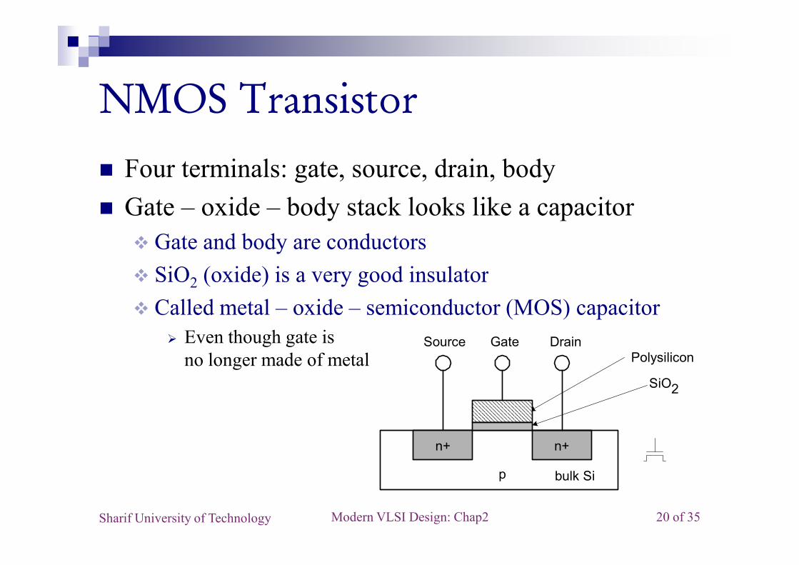
NMOS Transistor� Four terminals: gate, source, drain, body� Gate – oxide – body stack looks like a capacitor

� Gate and body are conductors� SiO2 (oxide) is a very good insulator

Modern VLSI Design: Chap2 20 of 35Sharif University of Technology

2 ( ) y g� Called metal – oxide – semiconductor (MOS) capacitor

� Even though gate isno longer made of metal

n+

p

GateSource Drain

bulk Si

SiO2

Polysilicon

n+

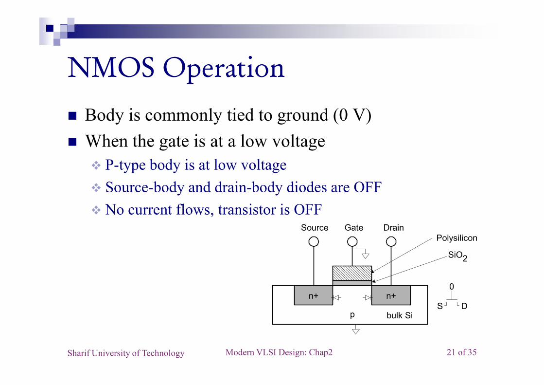
NMOS Operation� Body is commonly tied to ground (0 V)� When the gate is at a low voltage

� P-type body is at low voltage� Source-body and drain-body diodes are OFF

Modern VLSI Design: Chap2 21 of 35Sharif University of Technology

y y� No current flows, transistor is OFF

n+

p

GateSource Drain

bulk Si

SiO2

Polysilicon

n+D

0

S

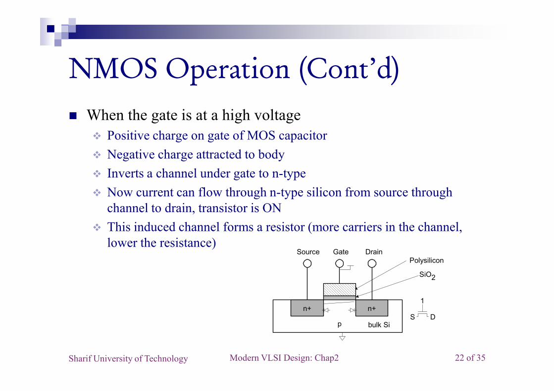
� When the gate is at a high voltage� Positive charge on gate of MOS capacitor� Negative charge attracted to body� Inverts a channel under gate to n-type� Now current can flow through n-type silicon from source through

NMOS Operation (Cont’d)

Modern VLSI Design: Chap2 22 of 35Sharif University of Technology

� Now current can flow through n type silicon from source throughchannel to drain, transistor is ON

� This induced channel forms a resistor (more carriers in the channel,lower the resistance)

n+

p

GateSource Drain

bulk Si

SiO2

Polysilicon

n+D

1

S

� Poly-oxide-silicon sandwich under the gate is acapacitor�To increase voltage, need to add positive charge to

l d i h ili

NMOS Operation (Cont’d)

Modern VLSI Design: Chap2 23 of 35Sharif University of Technology

poly and negative charge to silicon� Initially, negative charge comes from pushing

away holes� After threshold voltage is reached, channel of

mobile electrons formed

PMOS Transistor� Channel carriers have positive charge� Similar, but doping and voltages reversed

� Body tied to high voltage (VDD)� Gate low: transistor ON

� Attracts holes to form a thin p-region allows holes to flow from p+ to p+� G t hi h t i t OFF

Modern VLSI Design: Chap2 24 of 35Sharif University of Technology

� Gate high: transistor OFF� When channel not formed, p+ regions are isolated by back-to-back diodes

� Bubble indicates inverted behavior

SiO2

n

GateSource Drain

bulk Si

Polysilicon

p+ p+

Drain current characteristics

Modern VLSI Design: Chap2 25 of 35Sharif University of Technology
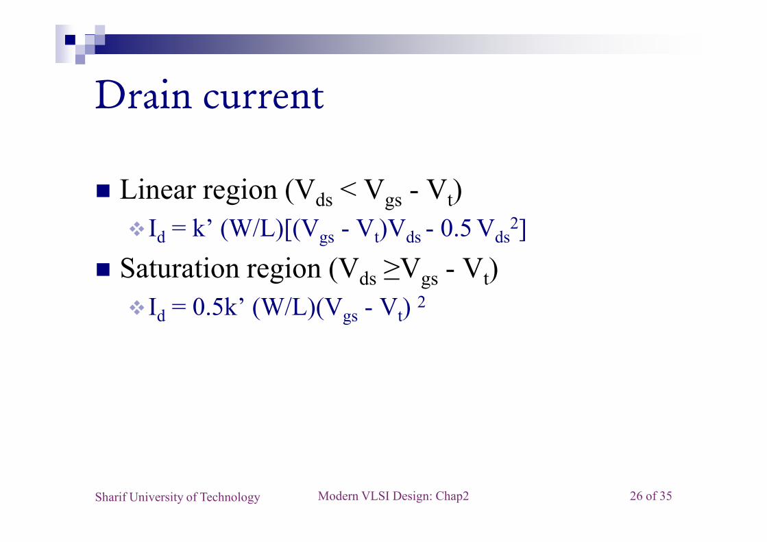
Drain current

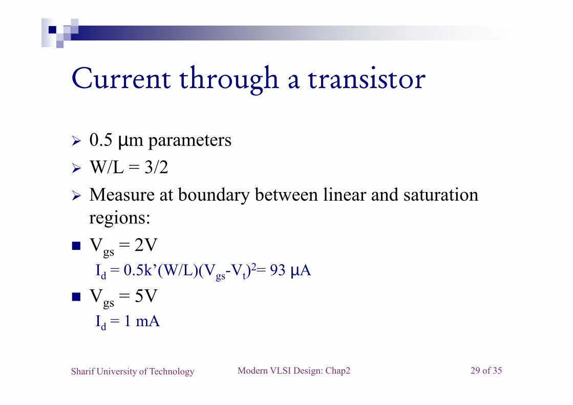
� Linear region (Vds < Vgs - Vt)�Id = k’ (W/L)[(Vgs - Vt)Vds - 0.5 Vds

2]� Saturation region (V ≥V - V )

Modern VLSI Design: Chap2 26 of 35Sharif University of Technology

� Saturation region (Vds ≥Vgs - Vt)�Id = 0.5k’ (W/L)(Vgs - Vt) 2

Power Supply Voltage

� GND = 0 V� In 1980’s, VDD = 5V� VDD has decreased in modern processes

Modern VLSI Design: Chap2 27 of 35Sharif University of Technology

� VDD has decreased in modern processes�High VDD would damage modern tiny transistors�Lower VDD saves power

� VDD = 3.3, 2.5, 1.8, 1.5, 1.2, 1.0, …

0.5 µm transconductances

From a MOSIS process:� n-type:

�k ’ = 73 µA/V2

Modern VLSI Design: Chap2 28 of 35Sharif University of Technology

�kn = 73 µA/V�Vtn = 0.7 V

� p-type:�kp’ = 21 µA/V2

�Vtp = -0.8 V

Current through a transistor

� 0.5 µm parameters� W/L = 3/2� Measure at boundary between linear and saturation

Modern VLSI Design: Chap2 29 of 35Sharif University of Technology

yregions:

� Vgs = 2VId = 0.5k’(W/L)(Vgs-Vt)2= 93 µA

� Vgs = 5VId = 1 mA

Outline

� Fabrication steps� Transistor structures� Transistor behavior

Modern VLSI Design: Chap2 30 of 35Sharif University of Technology

� Transistor behavior�NMOS�PMOS

� Latch up

Latch-up

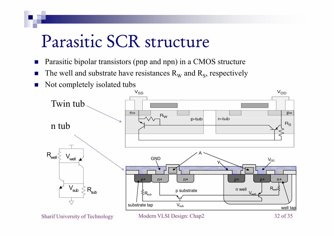
� CMOS ICs have parastic silicon-controlled rectifiers(SCRs)

� When powered up

Modern VLSI Design: Chap2 31 of 35Sharif University of Technology

� SCRs can turn on� Creating low-resistance path from power to ground� Current can destroy chip

� Early CMOS problem� Can be solved with proper circuit/layout structures

Parasitic SCR structure� Parasitic bipolar transistors (pnp and npn) in a CMOS structure� The well and substrate have resistances RW and RS, respectively� Not completely isolated tubs

Twin tub

Modern VLSI Design: Chap2 32 of 35Sharif University of Technology

n+

p substrate

p+

A

YGND VDD

n+p+

substrate tap well tap

n+ p+

n wellRsub

Rwell

Vsub

VwellRsub

Rwell

Vsub

Vwell

n tub

Parasitic SCR� Two modes of operation:

� Both BJTs off� Both BJTs saturated � short circuit power supply

Modern VLSI Design: Chap2 33 of 35Sharif University of Technology

circuit I-V behavior

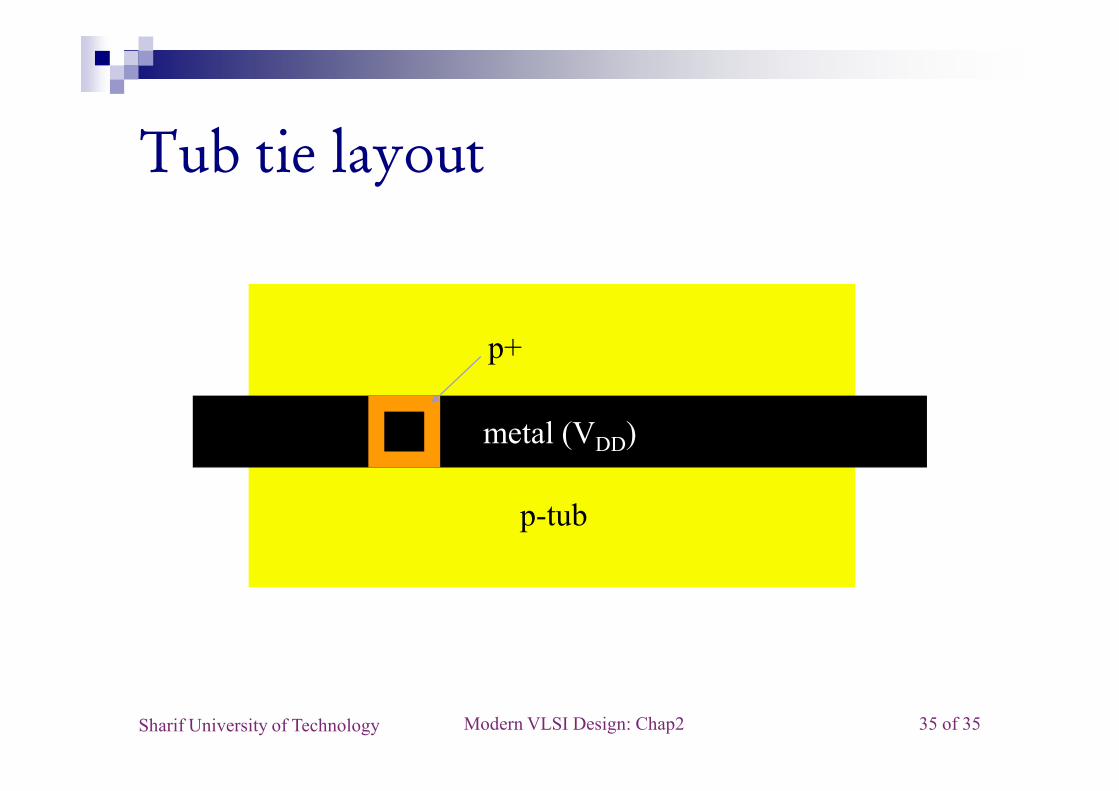
Solution to latch-up� Use tub ties with small resistance to connect tub to

power rail� n+ (heavily doped): low resistance

� Use enough to create low-voltage connection

Modern VLSI Design: Chap2 34 of 35Sharif University of Technology

� Use enough to create low voltage connection

Tub tie layout

p+

Modern VLSI Design: Chap2 35 of 35Sharif University of Technology

metal (VDD)

p-tub


Recommended