Application ReportSLVA862A–December 2016–Revised April 2018
Basics of eFuses
Rakesh Panguloori....................................................................................................... Power Switches
ABSTRACTeFuses are integrated power path protection devices that are used to limit circuit currents, voltages to safelevels during fault conditions. eFuses offer many benefits to the system and can include protectionfeatures that are often difficult to implement with discrete components. This application note highlights thechallenges and limitations of discrete circuit-protection solutions and discusses how they can be improvedwith an eFuse. This report also provides an example comparison between eFuse solution and discretecircuit-protection solution for a typical hard disk drive (HDD) application.
Contents1 Need for Protection and Ways to Achieve................................................................................ 22 Discrete Circuit-Protection Solutions ...................................................................................... 23 What is an eFuse?........................................................................................................... 44 Typical Application Example for Comparison........................................................................... 115 Conclusion .................................................................................................................. 126 References .................................................................................................................. 12
List of Figures
1 Typical Discrete Protection Circuit......................................................................................... 32 Active Current Protection Circuit Using Discrete Components ........................................................ 33 Block Diagram of eFuse .................................................................................................... 44 Overload Response of eFuse With Current-Limiting Function......................................................... 55 Overload Response of eFuse With Circuit-Breaker Function.......................................................... 56 Fast-Trip Current............................................................................................................. 67 Short-Circuit Response of TPS259241 With ILIM Set to 5 A ............................................................ 68 Fast-Trip Comparator Response for a Hot-Short Fault ................................................................. 69 Reverse Current Protection Using (a) Diode (b) External MOSFET and Ideal Diode Controller (c) eFuse ..... 610 Output Voltage-Cutoff for an Overvoltage Fault ........................................................................ 711 Output Voltage-Clamp during Transient Input Overvoltage ............................................................ 712 TPS25942L: Latched for Short-Circuit Fault ............................................................................. 813 TPS25942A: Auto-Retry and Recovery From Short Circuit ........................................................... 814 Input Reverse Polarity Protection Using (a) Diode (b) P-MOSFET (c) Fuse + TVS Diode (d) TPS2600 eFuse 915 Surge Protection Solution Using TPS2660 eFuse ...................................................................... 916 Circuit Implementation With Quick Output Discharge Function ...................................................... 10
TrademarksAll trademarks are the property of their respective owners.
1 Need for Protection and Ways to AchieveModern electronic systems are designed with high level of integration to offer superior performance withmultitude of functionality. These systems use multi-voltage power distribution to support various types ofloads for their proper operation. One of the major expectations is the minimal system downtime during anytransient abnormal events such as overload or short-circuit conditions. For example, while hot-plugging ahard disk drive into a storage system, huge inrush current can result in voltage sag on the connected busand eventually affect other operating loads on the same bus. To overcome this scenario, today’s systemdesigners use protection devices to manage inrush, overload, short circuit, and overvoltage events and toguard the sensitive loads for reliable system operation. The key requirement is to bring down the faultcurrents within the limits and bring the system back to active state once the fault is cleared, without anymanual intervention.
Fuses, positive temperature coefficient (PTC) resistors, and active circuit protection are a few of theprotection devices with varied capabilities and drawbacks. Fuses are traditionally considered as protectiondevices used to isolate overload or short-circuit faults from the main system. Although these devicesprovide protection, the fault current needs to be exceedingly higher than the rating of the fuse withresponse time ranging from milliseconds to seconds. This makes it extremely difficult to predict the preciseovercurrent level at which the fuse will open. A conservative selection on fuse current rating may lead tofuse blowup during inrush current events. In addition, once the fuse blows during an overload event, it hasto be physically replaced, which increases system down time and maintenance costs. On the other hand,PTC resistors provide resettable overcurrent protection and, unlike a fuse, these can avoid the physicalintervention. However, because they are actuated by the heating effect of an overcurrent load, theirreaction time is limited to several milliseconds. Also the ON-resistance of PTC fuse increases after everyreset, which raises concerns on achieving repeatable performance over time.
The best way to prevent system downtime is to detect, respond and correct potentially damagingconditions as quickly as possible. As the response of fuse and PTC resistors depends on heating effect(temperature, a lagging parameter) for their operation, many system designers prefer to use a leadingindicator, current, to provide effective circuit protection. Both fuse and PTC resistors do not cover many ofthe protection requirements such as inrush control, overvoltage; reverse current, reverse polarityprotections needed in modern electronic systems. The next section describes the active circuit-protectionsolutions using discrete components and the challenges involved.
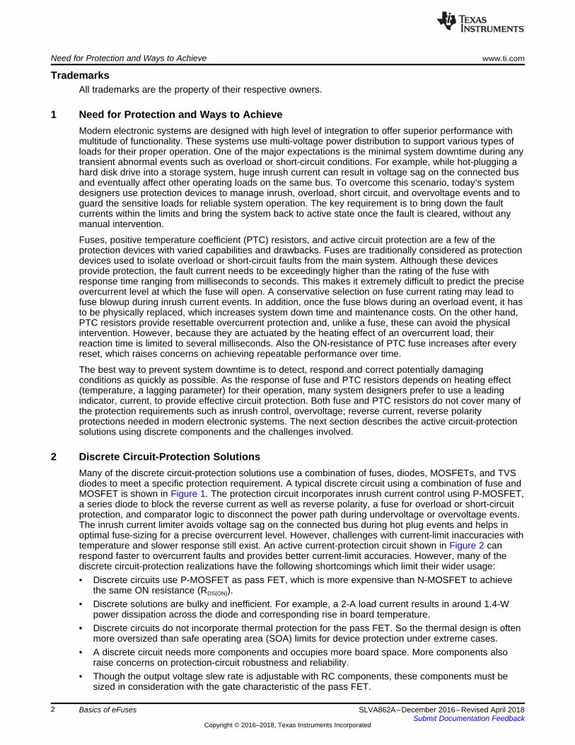
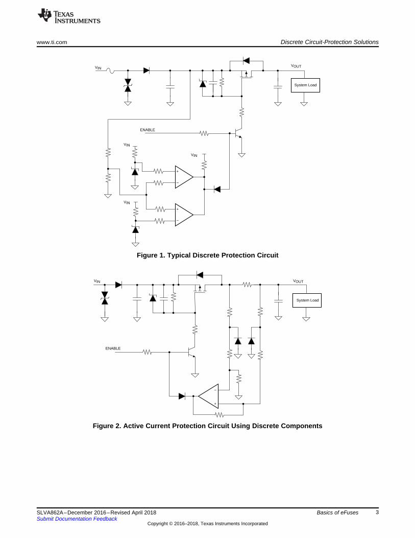
2 Discrete Circuit-Protection SolutionsMany of the discrete circuit-protection solutions use a combination of fuses, diodes, MOSFETs, and TVSdiodes to meet a specific protection requirement. A typical discrete circuit using a combination of fuse andMOSFET is shown in Figure 1. The protection circuit incorporates inrush current control using P-MOSFET,a series diode to block the reverse current as well as reverse polarity, a fuse for overload or short-circuitprotection, and comparator logic to disconnect the power path during undervoltage or overvoltage events.The inrush current limiter avoids voltage sag on the connected bus during hot plug events and helps inoptimal fuse-sizing for a precise overcurrent level. However, challenges with current-limit inaccuracies withtemperature and slower response still exist. An active current-protection circuit shown in Figure 2 canrespond faster to overcurrent faults and provides better current-limit accuracies. However, many of thediscrete circuit-protection realizations have the following shortcomings which limit their wider usage:• Discrete circuits use P-MOSFET as pass FET, which is more expensive than N-MOSFET to achieve
the same ON resistance (RDS(ON)).• Discrete solutions are bulky and inefficient. For example, a 2-A load current results in around 1.4-W
power dissipation across the diode and corresponding rise in board temperature.• Discrete circuits do not incorporate thermal protection for the pass FET. So the thermal design is often
more oversized than safe operating area (SOA) limits for device protection under extreme cases.• A discrete circuit needs more components and occupies more board space. More components also
raise concerns on protection-circuit robustness and reliability.• Though the output voltage slew rate is adjustable with RC components, these components must be
sized in consideration with the gate characteristic of the pass FET.
3 What is an eFuse?An integrated circuit protection solution called “eFuse” can overcome the limitations with discrete circuitprotection realizations. An eFuse is an “active circuit protection device with an integrated FET used to limitcurrents, voltages to safe levels during fault conditions”. It embeds various functions to protect systemagainst inrush current, overcurrent, overvoltage, reverse current, reverse polarity and short circuit faults.The eFuse is more accurate, faster and can ‘repair’ itself without user intervention. Most of the TI eFusesare recognized as Solid State Overcurrent Protectors under the UL2367 standard. Also these are certifiedunder safety standard UL 60950 and are safe to use.
Figure 3 shows a block diagram of an eFuse. An understanding of the functionality of various features inan eFuse helps in choosing the right eFuse for a particular application. This section discusses thefunctionality of each feature the eFuse offers. As shown in Figure 3, an eFuse requires very few externalcomponents (resistor RILIM for current limit setting and a capacitor CdVdT for setting the output voltage ramprate) resulting in significant board space saving and robust protection when compared to discretesolutions.
Figure 3. Block Diagram of eFuse
3.1 Inrush Current ControlInrush currents are a major concern in DC power systems. For example, while hot-plugging a hard diskdrive into a storage system, huge inrush current can result due to quickly charging its filter or loadcapacitor. This huge inrush current with fast slew rate causes voltage sag on the backplane which couldaffect operation of other connected loads. This problem can be solved by controlling the output voltageramp rate, thereby limiting the inrush current and disturbance on the backplane. Discrete circuits(Figure 1, Figure 2) use RC components around pass FET for inrush current control, which must be sizedin consideration with the gate characteristic of the pass FET and the load. Sometimes, it needs manydesign iterations to keep inrush current within the desired limit. If the input power is cycled rapidly, theload capacitor gets discharged quickly while the external gate capacitor remains charged and maintainspass FET in the ON condition. This inhibits the current-limiting feature allowing a large current surge whenpower is restored.
In an eFuse, the output voltage ramp rate is inversely proportional to the CdVdT capacitor value and can beconfigured easily at the desired rate. The built-in overtemperature protection in an eFuse prevents devicefailure that could happen due to severe dynamic power stress during startup. Refer to Section 4 for theinrush performance comparison between eFuse and a discrete solution.
3.2 Overcurrent ProtectionWhen an overcurrent event happens, protection for the downstream circuitry from excessive currents isessential to avoid any potential circuit damage or fire. The active current protection circuit shown inFigure 2 uses an external current sense resistor and a fast comparator for overcurrent protection. Thiscircuit realization often needs tradeoff between accuracy, cost, and power loss. TI eFuses provide activecurrent protection either by limiting the fault current (called current-limiting operation) or by breaking thefault circuit after an overload timeout (called circuit-breaker operation). The latest devices, such as theTPS25942 and TPS25944, offer ±8% current-limit accuracy over the load range of 0.6 A to 5.3 A.
An eFuse with the current-limiting feature limits the output current to a threshold set by an external resistorRILIM. Figure 4 shows the current-limit response of the TPS25942A eFuse, with the current limit (ILIM) set to5 A. For an overload condition, the eFuse limits the input current to 5 A until either the overload isremoved or the eFuse junction temperature TJ reaches thermal shutdown temperature (typically TTSD =150°C). Once the eFuse enters thermal shutdown, it either remains in the OFF position (a latch-offversion) or attempts to restart after TJ falls below TTSD by 12°C and with auto retry delay (128 ms forTPS25942A, an auto-retry device). It is observed in Figure 4, the TPS25942A makes circuit closure afterevery thermal shutdown and finally restores to normal condition when the overload fault is cleared. Thecurrent-limiting feature is beneficial in applications such as solid-state drives (SSDs), especially if theovercurrent event is temporary and to avoid system downtime.
Figure 4. Overload Response of eFuse With Current-Limiting Function
Figure 5. Overload Response of eFuse With Circuit-Breaker Function
For sensitive loads, such as a hard drive in data servers, an immediate power path opening is a safeoption in response to an overcurrent fault. An eFuse TPS25944A provides circuit-breaker operation withoverload timeout. When the load current exceeds the set current limit of 5 A, the TPS25944A starts thefault timer and breaks the circuit path if the load current does not fall below ILIM before the fault timerexpires (4 ms). Figure 5 shows circuit-breaker response of the TPS25944A eFuse, and since theTPS25944A is an auto retry device, it attempts to restart after a circuit-breaker retry delay of 128 ms. Thecircuit-breaker feature essentially avoids system downtime by allowing pulsed overloads at the output for afault period interval of 4 ms..
3.3 Short-Circuit ProtectionOne of the advantages of an eFuse over discrete solutions is the ability to respond faster for hot-shortfaults at the output. During a transient short-circuit event, the current through the eFuse increases veryrapidly. The current-limit amplifier of an eFuse cannot respond very quickly due to its limited bandwidth. TIeFuses incorporate a fast-trip current comparator, which shuts down the pass FET very quickly when theload current IOUT > fast-trip current threshold IFASTRIP. This terminates the rapid short-circuit peak current inless than 200 ns as shown in Figure 8. The fast trip threshold is set to 60% higher than the programmedoverload current limit (IFASTRIP = 1.6 × ILIM). After the transient short-circuit peak current has beenterminated by the fast-trip comparator, the current-limit amplifier smoothly regulates the output current toILIM as shown in Figure 7. If during current-limit operation, power dissipation of the pass FET [(VIN –VOUT) × IOUT] exceeds 10 W, there is approximately a 0 to 15% thermal fold back in the current-limit valueso that ILIM drops to ISC. Eventually, the device shuts down due to over temperature.
Figure 7. Short-Circuit Response of TPS259241 With ILIMSet to 5 A
Figure 8. Fast-Trip Comparator Response for a Hot-ShortFault
3.4 Reverse Current ProtectionReverse currents can flow through the system when the voltage at the output is higher than at the input. Inapplications such as power muxing for redundant power systems or SSD with a large hold-up outputcapacitor, there is a risk of large reverse currents when the input power is disconnected. The reversecurrent can damage internal circuitry or system power supplies, if it is not limited. For certain applicationssuch as PLC controller modules, this feature is mandatory to pass ‘voltage interruption tests’.
Figure 9. Reverse Current Protection Using (a) Diode (b) External MOSFET and Ideal Diode Controller (c)eFuse
A series diode can block reverse currents but results in significant power loss in the system which couldlower the system efficiency and battery life. An external MOSFET with an ideal diode controller IC (shownin Figure 9(b)) is a more efficient option and also offers flexibility in current support; however, it occupiesmore board space. TI's TPS2594 family of eFuses integrates blocking FET and a fast reverse comparatorto provide true reverse current blocking. When an input power fail condition is detected, the internal FET isturned OFF in 1 µs (typical). True reverse current blocking facilitates simplified efficient power muxing inredundant power systems. For additional information regarding power multiplexing using eFuses, seereference (1).
3.5 Overvoltage ProtectionTransient induced voltages or inductive switching can cause overvoltage in the system which lasts from afew hundred microseconds to milliseconds. An eFuse with output voltage-cutoff guards the sensitivecircuits from overvoltage by turning OFF the internal FET. The trip point for overvoltage cutoff can beprogrammable through an external resistor at the OVP pin of eFuse. As shown in Figure 10, theTPS25942x remains active for a nominal 12-V input voltage. When the input voltage exceeds theovervoltage trip point (16.5 V here), the eFuse turns OFF the internal FET causing the output voltageVOUT to fall to zero. The eFuse remains in the OFF condition as long as the input voltage exceeds theset overvoltage trip point. Once the input voltage returns to nominal operating voltage, the device turnsback ON and VOUT once again returns to 12 V. The latest eFuse device, TPS2660, protects the load upto 60-V DC Safe Extra Low Voltage (SELV) faults and is suitable for industrial applications.
Figure 10. Output Voltage-Cutoff for an Overvoltage Fault Figure 11. Output Voltage-Clamp during Transient InputOvervoltage
Some of the TI eFuses have an output voltage-clamp (OVC) feature, which keeps eFuse in operation byclamping the output voltage to the nominal voltage. As shown in Figure 11, the TPS25926x eFuseintegrates a 15-V output voltage-clamp. When the input voltage exceeds the internal OVC trip point, theinternal clamping circuitry activates and limits the output voltage to 15.6 V (typically 15 V). If the transienton the input is only temporary, the eFuse hides the overvoltage fault from downstream circuitry. If the faultlasts long enough to activate the eFuse’s thermal shutdown (typically TJ = 150°C), then the fault will stillcause the eFuse to turn OFF (similar to output voltage-cutoff).
3.6 Over Temperature ProtectionDiscrete protection realizations need careful selection of pass FET and thermal design to keep the devicein SOA limits under any extreme fault conditions. However, TI eFuses come with inbuilt over temperatureprotection and gets shutdown if the eFuse junction temperature, TJ, exceeds 150°C (typ). Once eFuseenters thermal shutdown, it either remains in the OFF position (a latch-off version) or attempts to restart(an auto retry version) after TJ falls below TTSD by 12°C and with auto retry delay.
3.7 Fault Response and RecoveryTI eFuses are available in two versions; latch off and auto retry. A latch-off version remains in the OFFposition and needs power recycle to turn ON again. A system with the latch-off version provides moresafety by immediately isolating the faulty component but also reduces the system uptime. Figure 12 showsthe short-circuit response of the latched device TPS25942L, where the device provides a limited current of5 A before getting into thermal shutdown. A reset at the enable pin is required to bring the device backinto operation. On the other hand, a device with auto retry continues to power cycle itself until the fault iscleared. As shown in Figure 13, the device TPS25942A attempts to power cycle after retry delay (128 ms)and resumes normal operation when short circuit is cleared. Since, over-temperature protection is inbuilt,no special thermal considerations are required for surviving a prolonged output short.
Figure 12. TPS25942L: Latched for Short-Circuit Fault Figure 13. TPS25942A: Auto-Retry and Recovery FromShort Circuit
3.8 Input Reverse Polarity ProtectionIn applications such as PLC systems, the input side needs reverse polarity protection against any fieldsupply mis-wiring. A blocking diode is the simplest means of protecting against reverse polarityconnections. Since no control signal is required, circuit complexity and component count are low. On theother hand, the diode dissipates energy all the time due to its forward voltage (VF) drop, which can causesignificant power loss in high-current applications and needs thermal management. Another approach is touse a P-MOSFET, which can be implemented with simpler drive circuitry comprising a Zener diode and aresistor, as shown in Figure 14(b). A P-MOSFET based solution is expensive and has the risk of failurewhen the input power is removed causing the output capacitor discharge through the fully enhanced P-MOSFET. Another simple solution, shown in Figure 14(c), uses a combination of fuse and TVS diode,where the fuse blows and protects the load against reverse polarity. But after the fault, the fuse needs tobe replaced. As shown in Figure 14(d), the TI eFuse TPS2660 integrates a reverse input polarityprotection circuit and does not need any external components. The TPS2660 ensures that the device isnot functional during reverse polarity conditions and internal FET blocks the reverse current path.
3.9 Surge ProtectionThe TPS2660 eFuse-based surge protection solution (reference (2)) is shown in Figure 15. It requires onlya single TVS diode to protect the load from surges. The device does not need any passive wave shapingcircuits to reduce the slew rate of the surge. It can handle slew rates as fast as 20 V/µs. Built-in back-to-back FETs and reverse polarity protection circuits effectively block negative voltage that can be generateddue to a negative surge. The ±70-V transient absolute maximum ratings of the TPS2660 device enablethe use of a single TVS diode for clamping the surge. Overvoltage and undervoltage protection makessure that the downstream converters are isolated from input when the surge is at peak or valley level. Aproprietary high-speed protection algorithm immediately disconnects the output from the input andprevents the surge passing from the input to the output.
Figure 15. Surge Protection Solution Using TPS2660 eFuse
3.10 Controlled Power DownWhen the device is disabled, the output voltage is left floating and power down profile is entirely dictatedby the load. In some applications, this can lead to undesired activity as the load is not powered down to adefined state. Controlled output discharge can ensure the load is turned OFF completely and not in anundefined operational state. The BFET pin in the TPS25927x family of eFuses facilitates the quick outputdischarge (QOD) function as illustrated in Figure 16. When the device is disabled, the BFET pin pulls lowwhich enables the external P-MOSFET, Q1, for the discharge feature to function. The output voltagedischarge rate is dictated by the output capacitor, COUT, the discharge resistance, RDCHG, and the load.
Figure 16. Circuit Implementation With Quick Output Discharge Function
3.11 UL CertificationsMost of the TI eFuses are UL 2367 (solid-state overcurrent protectors) recognized which would help indesigning sections of the system as “limited energy” or “low power” circuits to expedite the UL certificationprocess. Additionally, these devices are also UL 60950 (safe during single-point failure) recognized, whichrestricts the voltage, current within the circuit limits under any single fault. For additional informationregarding benefits of UL recognition, the reader is directed to reference (3).
3.12 Additional Features
3.12.1 Health Monitoring and ReportingThe TPS2594xx family of eFuses provide advanced features such as precise load current monitor, voltagemonitoring, and fault flag. The current source at the IMON terminal of the TPS2594xx eFuse is configured tobe proportional to the current flowing through the device. A resistor from this pin to GND converts currentto proportional voltage, which can be used as a means of monitoring the health of the system.
The power good comparator has an internal reference of V(PGTHR) = 0.99 V at the negative terminal andthe positive terminal PGTH can be utilized for monitoring of either input or output of the device or anyother voltage rail in the system. The comparator output PGOOD is an open-drain, active-high signal,which can be used to indicate the status and control the downstream units for power sequencing. PGOODis asserted high when the internal FET is fully enhanced and the PGTH pin voltage is higher than internalreference, V(PGTHR), eliminating the need for a separate supply voltage supervisor chip.
The FLT open-drain output is asserted (active low) during undervoltage, overvoltage, reverse voltage,reverse current, and thermal shutdown conditions.
3.12.2 Diode ModeThe TPS25942x and TPS25944x family of eFuses incorporate the diode mode feature, where the powerpath from IN to OUT acts as a non-ideal diode rather than a FET. This feature is useful in power-muxapplications to switch over from master to slave supplies and vice-versa smoothly, when two supplies arewithin a diode drop of each other.
3.12.3 Low Power ModeThe TPS25940 eFuse provides a dedicated DevSleep interface terminal (DEVSLP) to drive the device tolow power mode. The DEVSLP terminal is compatible with standard hardware signals asserted from thehost controller. When pulled high, it puts the device in low power DevSleep mode. In this mode, thequiescent current consumption of the device is limited to less than 95 μA (typical) and the functionality ofseveral non-critical modes are disabled.
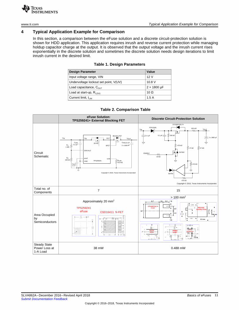
4 Typical Application Example for ComparisonIn this section, a comparison between the eFuse solution and a discrete circuit-protection solution isshown for HDD application. This application requires inrush and reverse current protection while managingholdup capacitor charge at the output. It is observed that the output voltage and the inrush current risesexponentially in the discrete solution and sometimes the discrete solution needs design iterations to limitinrush current in the desired limit.
Table 1. Design Parameters
Design Parameter ValueInput voltage range, VIN 12 VUndervoltage lockout set point, V(UV) 10.8 VLoad capacitance, COUT 2 × 1800 µFLoad at start-up, RL(SU) 10 ΩCurrent limit, ILIM 1.5 A
Table 2. Comparison Table
eFuse Solution:TPS259241+ External Blocking FET Discrete Circuit-Protection Solution
TPS259241+ External Blocking FET Discrete Circuit-Protection Solution
InrushPerformancewith RL(SU) =OPEN
InrushPerformancewith RL(SU) = 10Ω
5 ConclusionModern electronic systems need more than one type of protection. Though each of the protectionrequirements can be met with discrete components, the solution needs more board space, is less efficient,more expensive, and inferior in performance than TI’s integrated circuit protection solution “eFuse”. TheeFuse is more accurate, faster, and can ‘repair’ itself without user intervention. Most of the TI eFuses arerecognized as Solid State Overcurrent Protectors under UL2367 standard. Also these are certified undersafety standard UL 60950 and are safe during single point failure.
6 References1. Power Multiplexing Using Load Switches and eFuses (SLVA811)2. The TPS2660 Simplifies Surge and Power-Fail Protection Circuits in PLC System (SLVA833)3. How to save time and money with low power circuits
Changes from Original (December 2016) to A Revision ................................................................................................ Page
• Changed title of the Application Report to Basics of eFuses........................................................................ 1
IMPORTANT NOTICE FOR TI DESIGN INFORMATION AND RESOURCES
Texas Instruments Incorporated (‘TI”) technical, application or other design advice, services or information, including, but not limited to,reference designs and materials relating to evaluation modules, (collectively, “TI Resources”) are intended to assist designers who aredeveloping applications that incorporate TI products; by downloading, accessing or using any particular TI Resource in any way, you(individually or, if you are acting on behalf of a company, your company) agree to use it solely for this purpose and subject to the terms ofthis Notice.TI’s provision of TI Resources does not expand or otherwise alter TI’s applicable published warranties or warranty disclaimers for TIproducts, and no additional obligations or liabilities arise from TI providing such TI Resources. TI reserves the right to make corrections,enhancements, improvements and other changes to its TI Resources.You understand and agree that you remain responsible for using your independent analysis, evaluation and judgment in designing yourapplications and that you have full and exclusive responsibility to assure the safety of your applications and compliance of your applications(and of all TI products used in or for your applications) with all applicable regulations, laws and other applicable requirements. Yourepresent that, with respect to your applications, you have all the necessary expertise to create and implement safeguards that (1)anticipate dangerous consequences of failures, (2) monitor failures and their consequences, and (3) lessen the likelihood of failures thatmight cause harm and take appropriate actions. You agree that prior to using or distributing any applications that include TI products, youwill thoroughly test such applications and the functionality of such TI products as used in such applications. TI has not conducted anytesting other than that specifically described in the published documentation for a particular TI Resource.You are authorized to use, copy and modify any individual TI Resource only in connection with the development of applications that includethe TI product(s) identified in such TI Resource. NO OTHER LICENSE, EXPRESS OR IMPLIED, BY ESTOPPEL OR OTHERWISE TOANY OTHER TI INTELLECTUAL PROPERTY RIGHT, AND NO LICENSE TO ANY TECHNOLOGY OR INTELLECTUAL PROPERTYRIGHT OF TI OR ANY THIRD PARTY IS GRANTED HEREIN, including but not limited to any patent right, copyright, mask work right, orother intellectual property right relating to any combination, machine, or process in which TI products or services are used. Informationregarding or referencing third-party products or services does not constitute a license to use such products or services, or a warranty orendorsement thereof. Use of TI Resources may require a license from a third party under the patents or other intellectual property of thethird party, or a license from TI under the patents or other intellectual property of TI.TI RESOURCES ARE PROVIDED “AS IS” AND WITH ALL FAULTS. TI DISCLAIMS ALL OTHER WARRANTIES ORREPRESENTATIONS, EXPRESS OR IMPLIED, REGARDING TI RESOURCES OR USE THEREOF, INCLUDING BUT NOT LIMITED TOACCURACY OR COMPLETENESS, TITLE, ANY EPIDEMIC FAILURE WARRANTY AND ANY IMPLIED WARRANTIES OFMERCHANTABILITY, FITNESS FOR A PARTICULAR PURPOSE, AND NON-INFRINGEMENT OF ANY THIRD PARTY INTELLECTUALPROPERTY RIGHTS.TI SHALL NOT BE LIABLE FOR AND SHALL NOT DEFEND OR INDEMNIFY YOU AGAINST ANY CLAIM, INCLUDING BUT NOTLIMITED TO ANY INFRINGEMENT CLAIM THAT RELATES TO OR IS BASED ON ANY COMBINATION OF PRODUCTS EVEN IFDESCRIBED IN TI RESOURCES OR OTHERWISE. IN NO EVENT SHALL TI BE LIABLE FOR ANY ACTUAL, DIRECT, SPECIAL,COLLATERAL, INDIRECT, PUNITIVE, INCIDENTAL, CONSEQUENTIAL OR EXEMPLARY DAMAGES IN CONNECTION WITH ORARISING OUT OF TI RESOURCES OR USE THEREOF, AND REGARDLESS OF WHETHER TI HAS BEEN ADVISED OF THEPOSSIBILITY OF SUCH DAMAGES.You agree to fully indemnify TI and its representatives against any damages, costs, losses, and/or liabilities arising out of your non-compliance with the terms and provisions of this Notice.This Notice applies to TI Resources. Additional terms apply to the use and purchase of certain types of materials, TI products and services.These include; without limitation, TI’s standard terms for semiconductor products http://www.ti.com/sc/docs/stdterms.htm), evaluationmodules, and samples (http://www.ti.com/sc/docs/sampterms.htm).