KUPPAM ENGINEERING COLLEGE DEPARTMENT OF ELECTRICAL & ELECTRONICS ENGINEERING PRESENTED BY: S.FIRDOSE BEGUM 11F41A0239 B.V.PAVAN KUMAR :11F41A0204 R.BHABITHA :11F41A0236 P.JAYALAKSHMI :11F41A0233 UNDER THE GUIDANCE OF Mr P.KIRAN KUMAR M.Tech Assistant professor HIGH STEP-UP CONVERTER WITH THREE- WINDING COUPLED INDUCTOR
Transcript
KUPPAM ENGINEERING COLLEGE DEPARTMENT OFELECTRICAL & ELECTRONICS ENGINEERING
UNDER THE GUIDANCE OF Mr P.KIRAN KUMAR M.Tech Assistant professor
HIGH STEP-UP CONVERTER WITH THREE- WINDING COUPLED INDUCTOR
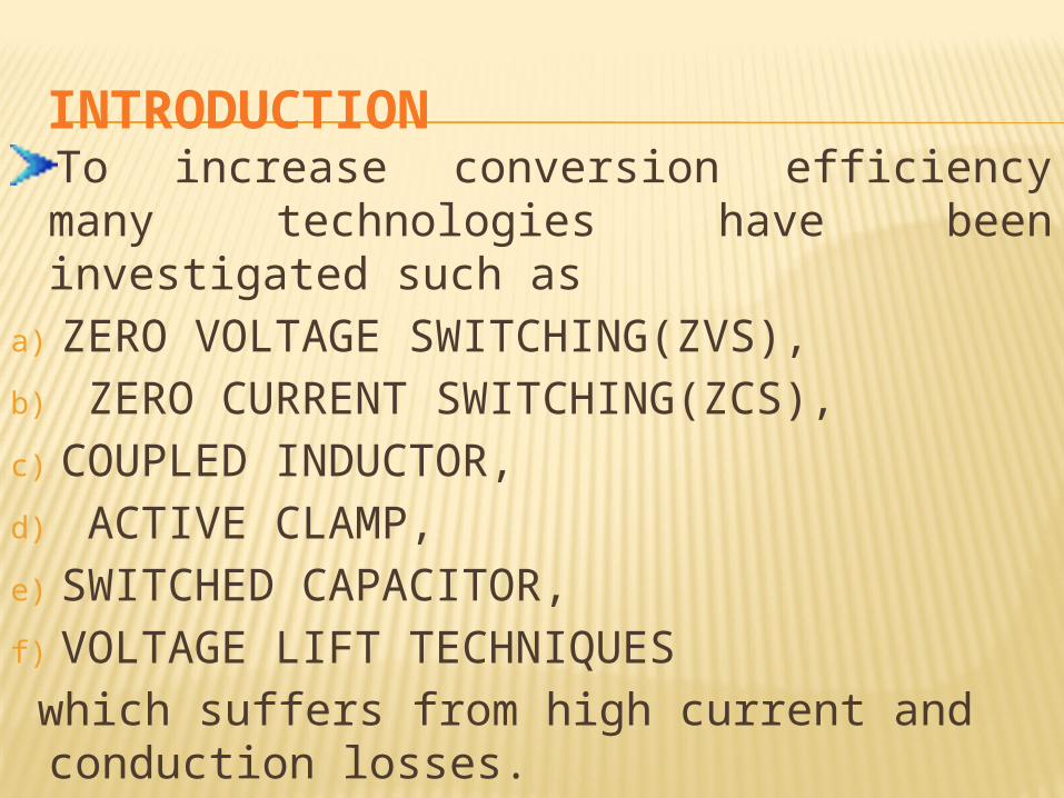
INTRODUCTION
To increase conversion efficiency many technologies have been investigated such as
a) ZERO VOLTAGE SWITCHING(ZVS),b) ZERO CURRENT SWITCHING(ZCS), c) COUPLED INDUCTOR,d) ACTIVE CLAMP,e) SWITCHED CAPACITOR,f) VOLTAGE LIFT TECHNIQUES which suffers from high current and
conduction losses.
CONTINUATION OF INTRODUCTIONRecently coupled inductor technique with performance of
i. Leakage energy recycle,ii. Adjustable voltage gain,iii.High efficiency continuous conduction mode,iv. Low voltage stress is developed.
It Avoids high peak current ripple, large input current ripple It employs a switched capacitor to supply an extra step up performance and voltage doubler circuit to lift the output voltage by increasing the turns ratio of coupled inductor.
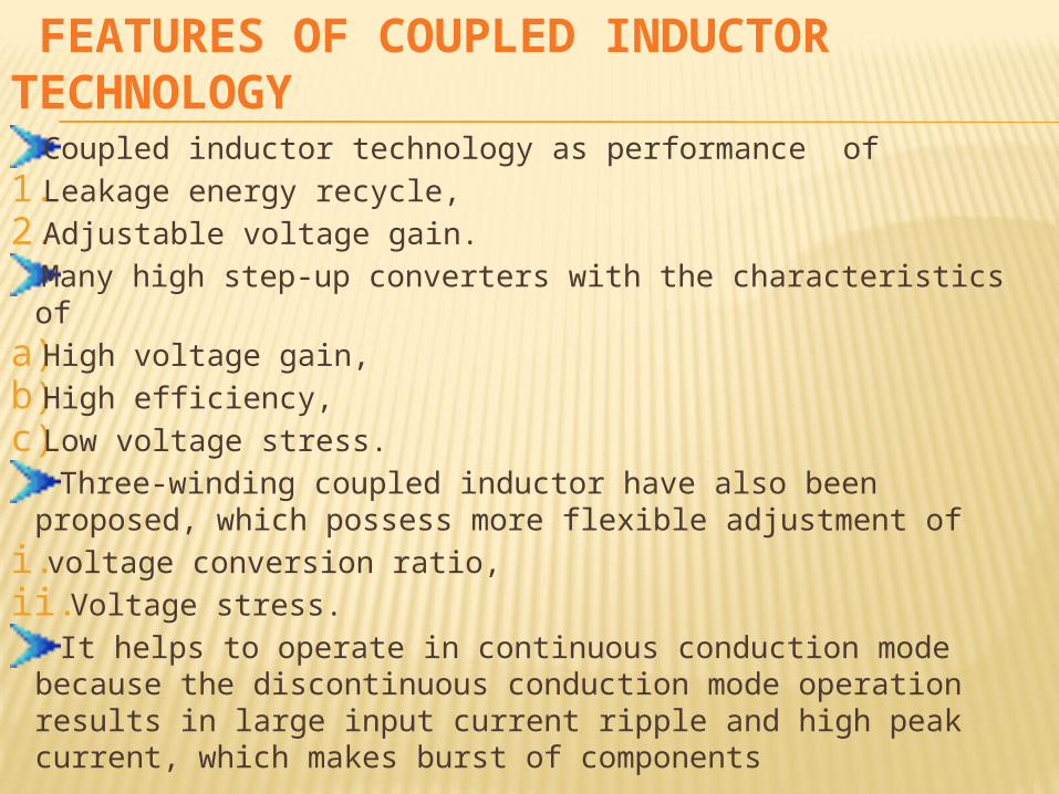
FEATURES OF COUPLED INDUCTOR TECHNOLOGY
Coupled inductor technology as performance of1. Leakage energy recycle,2. Adjustable voltage gain.
Many high step-up converters with the characteristics of a)High voltage gain,b)High efficiency,c) Low voltage stress.
Three-winding coupled inductor have also been proposed, which possess more flexible adjustment of
i. voltage conversion ratio,ii. Voltage stress.
It helps to operate in continuous conduction mode because the discontinuous conduction mode operation results in large input current ripple and high peak current, which makes burst of components
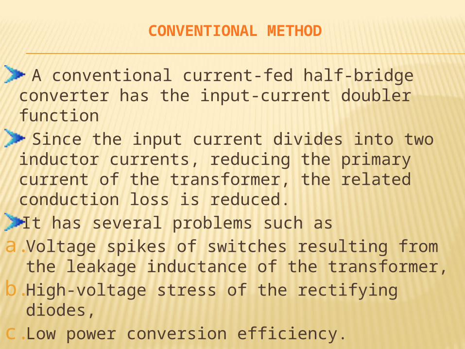
CONVENTIONAL METHOD
A conventional current-fed half-bridge converter has the input-current doubler function Since the input current divides into two inductor currents, reducing the primary current of the transformer, the related conduction loss is reduced.It has several problems such as
a.Voltage spikes of switches resulting from the leakage inductance of the transformer,
b.High-voltage stress of the rectifying diodes,c. Low power conversion efficiency.
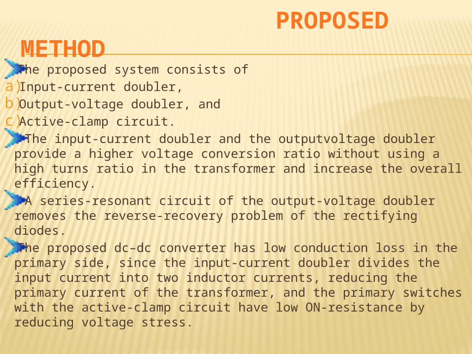
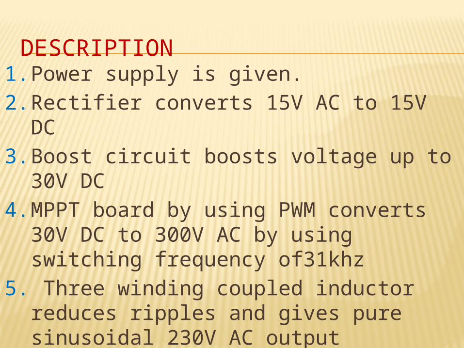
PROPOSED METHOD The proposed system consists of
a) Input-current doubler, b) Output-voltage doubler, and c) Active-clamp circuit.
The input-current doubler and the outputvoltage doubler provide a higher voltage conversion ratio without using a high turns ratio in the transformer and increase the overall efficiency. A series-resonant circuit of the output-voltage doubler removes the reverse-recovery problem of the rectifying diodes. The proposed dc–dc converter has low conduction loss in the primary side, since the input-current doubler divides the input current into two inductor currents, reducing the primary current of the transformer, and the primary switches with the active-clamp circuit have low ON-resistance by reducing voltage stress.
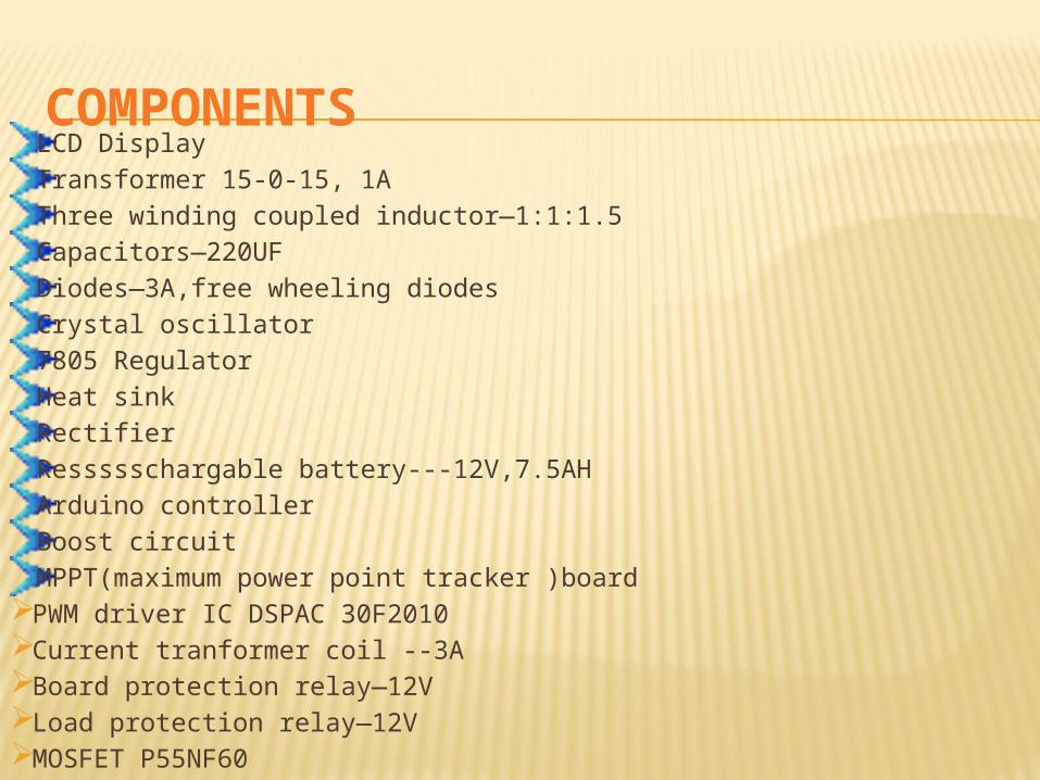
DESIGN CONSIDERATIONS
The required step-up conversion ratio is up to 6.7. Therefore, in order to make the duty cycle lower than 0.5 to decrease the conduction losses, the key design step is to determine the turns ratio of the coupled inductor.
Thus, the turns ratio of the coupled inductor is set as 1:1:1.5. The magnetizing inductor can be designed based on the current ripple
percentage of magnetizing inductor under full-load operation, and the related equations are given as
ILm ={(1 + n3)/( 1 − Dmax)} Io,max Lm = (Vin,min × Dmax) /(f × 2ΔiLm) The capacitors can be designed based on the voltage ripple
percentage of capacitor under full-load operation, and the related equations are given as
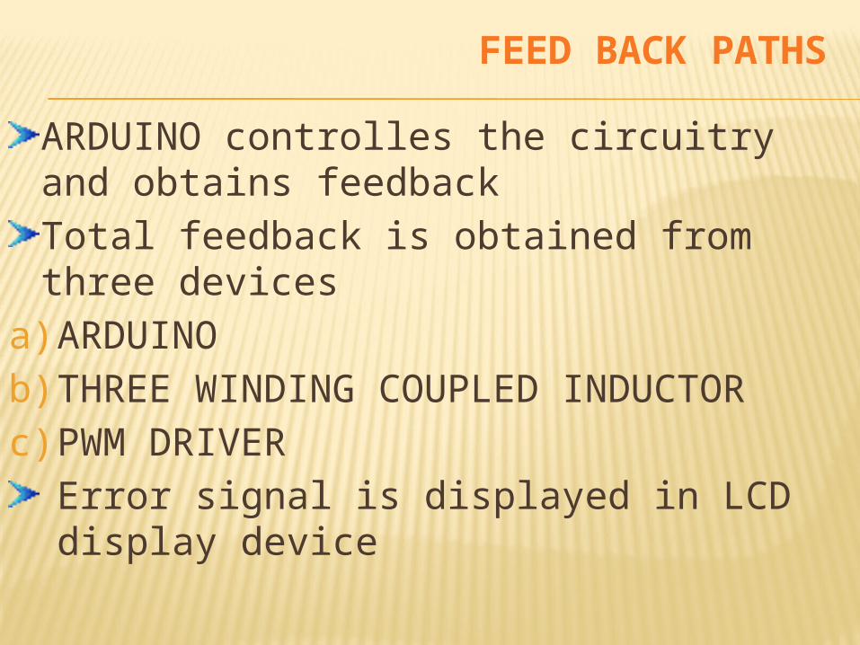
ARDUINO controlles the circuitry and obtains feedbackTotal feedback is obtained from three devices
a) ARDUINO b) THREE WINDING COUPLED INDUCTORc) PWM DRIVER
Error signal is displayed in LCD display device
ADVANTAGES Through adjusting the turns ratio of coupled inductor, the proposed converter achieves high step-up gain that renewable energy systems require;Leakage energy is recycled to the output terminal, which improves the efficiency and alleviates large voltage spikes across the main switch;Due to the passive lossless clamped performance, the voltage stress across main switch is substantially lower than the output voltage;Low cost and high efficiency are achieved by adopting low-voltage-rated power switch with low RDS-ON;By using three-winding coupled inductor, the proposed converter possesses more flexible adjustment of voltage conversion ratio and voltage stress on each diode
DISADVANTAGES AND THEIR ANALYSISAll the leakage inductors of coupled inductor are neglected and all of components are ideal without any parasitic components as energy recycling process occurs. The voltages are considered to be constant due to infinitely large capacitances.Some conduction losses are caused by resistances of semiconductor components and coupled inductor ,which is calculated by small ripple approximation.Large input current ripple and peak current is avoided as all currents passing through components were approximated by dc components. Thus, magnetizing current and capacitor voltages are assumed to be constant.
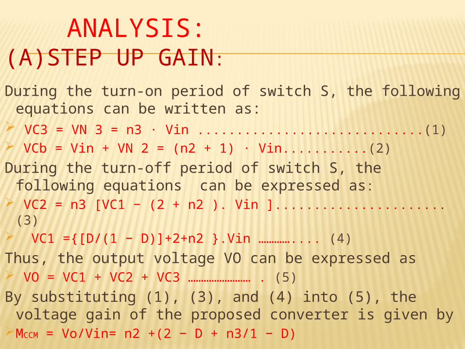
ANALYSIS:(A)STEP UP GAIN:
During the turn-on period of switch S, the following equations can be written as:
Thus, the output voltage VO can be expressed as VO = VC1 + VC2 + VC3 …………………… . (5)
By substituting (1), (3), and (4) into (5), the voltage gain of the proposed converter is given by
MCCM = Vo/Vin= n2 +(2 − D + n3/1 − D)
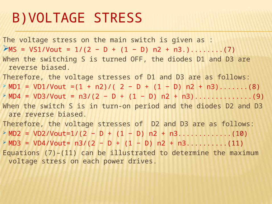
B)VOLTAGE STRESS
The voltage stress on the main switch is given as :MS = VS1/Vout = 1/(2 − D + (1 − D) n2 + n3.)........(7)
When the switching S is turned OFF, the diodes D1 and D3 are reverse biased.
Therefore, the voltage stresses of D1 and D3 are as follows: MD1 = VD1/Vout =(1 + n2)/( 2 − D + (1 − D) n2 + n3).......(8) MD4 = VD3/Vout = n3/(2 − D + (1 − D) n2 + n3)..............(9)
When the switch S is in turn-on period and the diodes D2 and D3 are reverse biased.
Therefore, the voltage stresses of D2 and D3 are as follows: MD2 = VD2/Vout=1/(2 − D + (1 − D) n2 + n3.............(10) MD3 = VD4/Vout= n3/(2 − D + (1 − D) n2 + n3..........(11)
Equations (7)–(11) can be illustrated to determine the maximum voltage stress on each power drives.
(C) CONDUCTION LOSSES:
Some conduction losses are caused by resistances of semiconductor components and coupled inductor ,which is calculated by small ripple approximation.Voltage conversion ratio with conduction losses is given as:
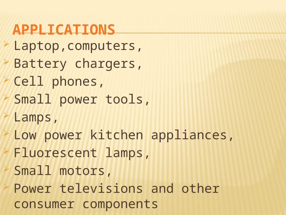
Laptop,computers, Battery chargers, Cell phones, Small power tools, Lamps, Low power kitchen appliances, Fluorescent lamps, Small motors, Power televisions and other consumer
components
CONCLUSION
By using technologies of three winding coupled inductor, switched capacitor, and voltage doubler circuit, the high step-up conversion can be efficiently obtained. The leakage energy is recycled and large voltage spike is alleviated; thus, the voltage stress is limited and the efficiency is improved.The low-voltage-rated switch with low RDS-ON can