Battery Energy Storage with an Inverter that Mimics Synchronous Generators Team 1508 Members Nerian Kulla Sabahudin Lalic David Hooper Faculty Advisor Professor Sung-Yeul Park To: ECE/CSE Faculty ECE 4901 Design Review 11/11/2014
Transcript
Battery Energy Storage with an Inverter that Mimics Synchronous Generators
Team 1508 Members Nerian Kulla
Sabahudin LalicDavid Hooper
Faculty AdvisorProfessor Sung-Yeul Park
To: ECE/CSE Faculty ECE 4901
Design Review11/11/2014
Outline
Background Information Project Goals Key Specifications Design- DC/DC Design- DC/AC Design- Final Integrated Design
Budget Time line
Background Information
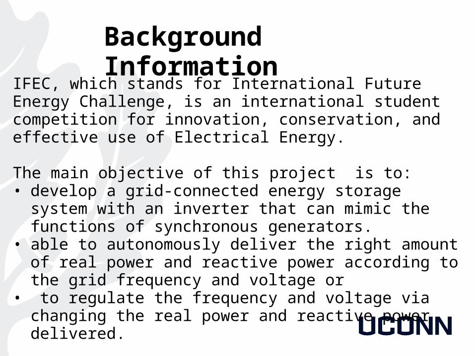
IFEC, which stands for International Future Energy Challenge, is an international student competition for innovation, conservation, and effective use of Electrical Energy.
The main objective of this project is to: • develop a grid-connected energy storage system with an inverter
that can mimic the functions of synchronous generators.• able to autonomously deliver the right amount of real power and
reactive power according to the grid frequency and voltage or• to regulate the frequency and voltage via changing the real power
and reactive power delivered.
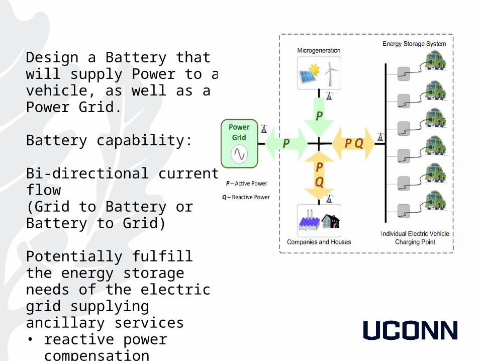
Design a Battery that will supply Power to a vehicle, as well as a Power Grid.
Battery capability:
Bi-directional current flow(Grid to Battery or Battery to Grid)
Potentially fulfill the energy storage needs of the electric grid supplying ancillary services • reactive power compensation• voltage regulation• and peak shaving
Project Goals Have the basic functions of charging,
discharging and protection for the battery Meet the desired power quality to the
grid/load Improve power density
Realize power conversion between the
battery and the gird/load with high
efficiency Achieve seamless transfer between grid-
connected and stand-alone modes Reduce manufacturing cost
Key Specifications
Design
Needs to be bidirectional It requires to Buck and Boost the voltage Convert voltage from DC to AC Convert voltage from AC to DC Be within the budget Be energy-efficient Meet the specifications
Requirements/Challenges:
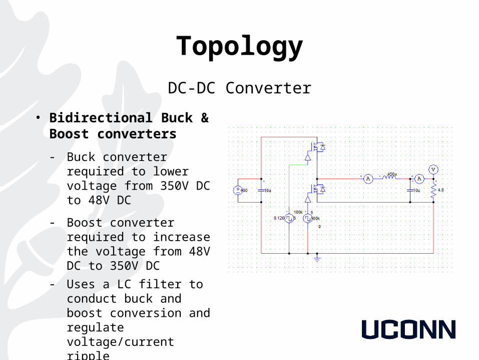
TopologyDC-DC Converter
• Bidirectional Buck & Boost converters
- Buck converter required to lower voltage from 350V DC to 48V DC
- Boost converter required to increase the voltage from 48V DC to 350V DC
- Uses a LC filter to conduct buck and boost conversion and regulate voltage/current ripple
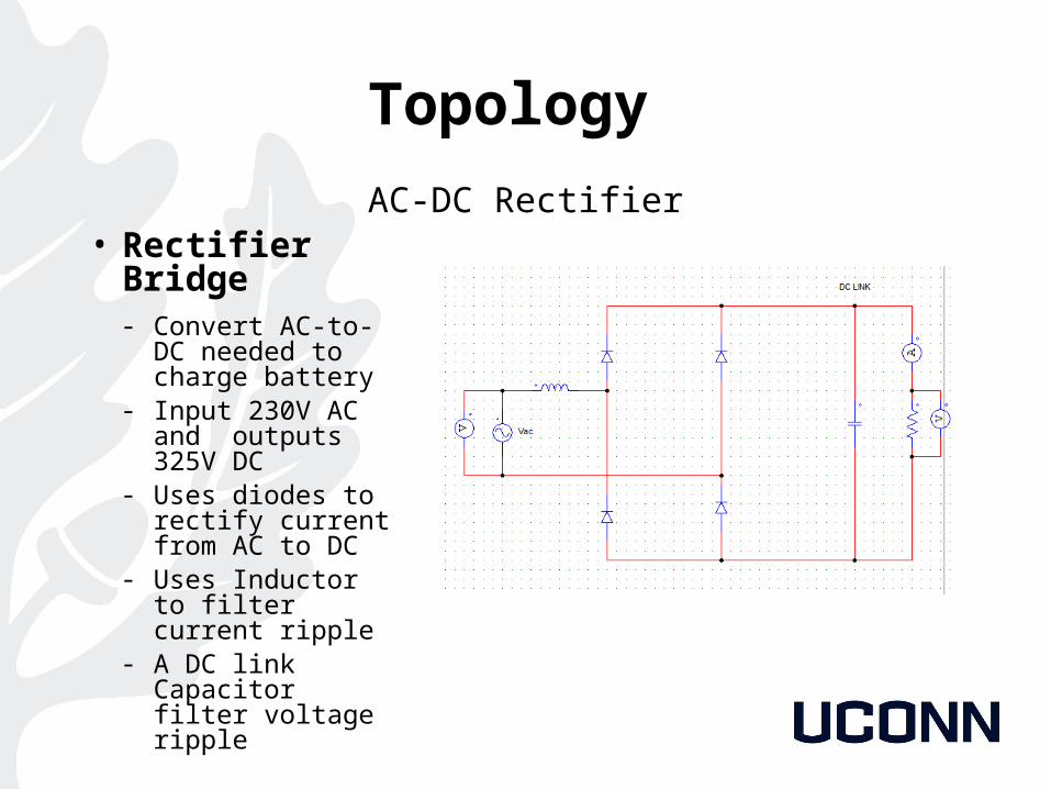
Topology AC-DC Rectifier
• Rectifier Bridge- Convert AC-to-DC
needed to charge battery
- Input 230V AC and outputs 325V DC
- Uses diodes to rectify current from AC to DC
- Uses Inductor to filter current ripple
- A DC link Capacitor filter voltage ripple
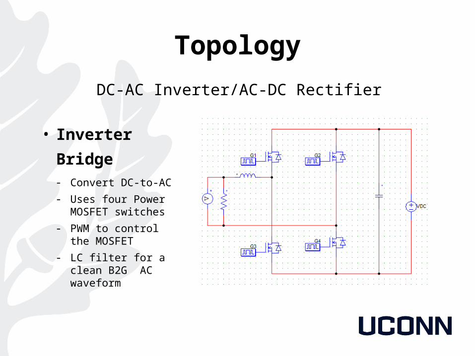
Topology
• Inverter Bridge- Convert DC-to-AC- Uses four Power MOSFET
switches- PWM to control the
MOSFET- LC filter for a clean B2G
AC waveform
DC-AC Inverter/AC-DC Rectifier
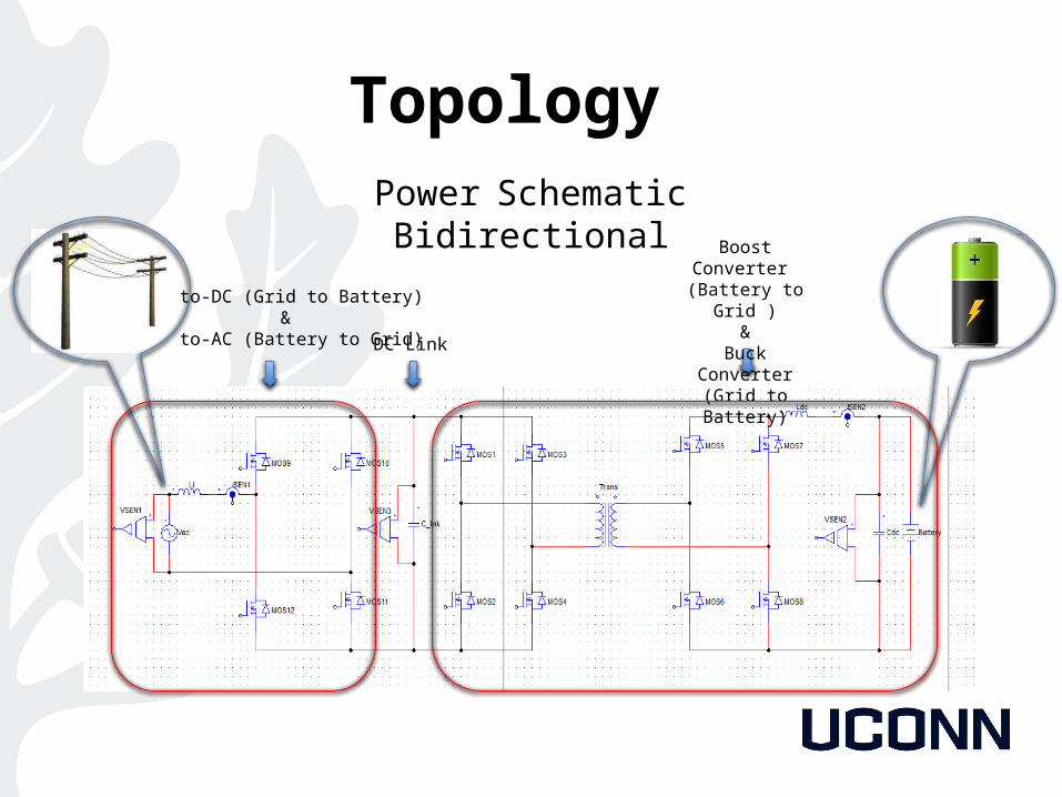
Power SchematicBidirectional
AC-to-DC (Grid to Battery)&
DC-to-AC (Battery to Grid) DC Link
Boost Converter (Battery to Grid )
&Buck Converter(Grid to Battery)
Topology
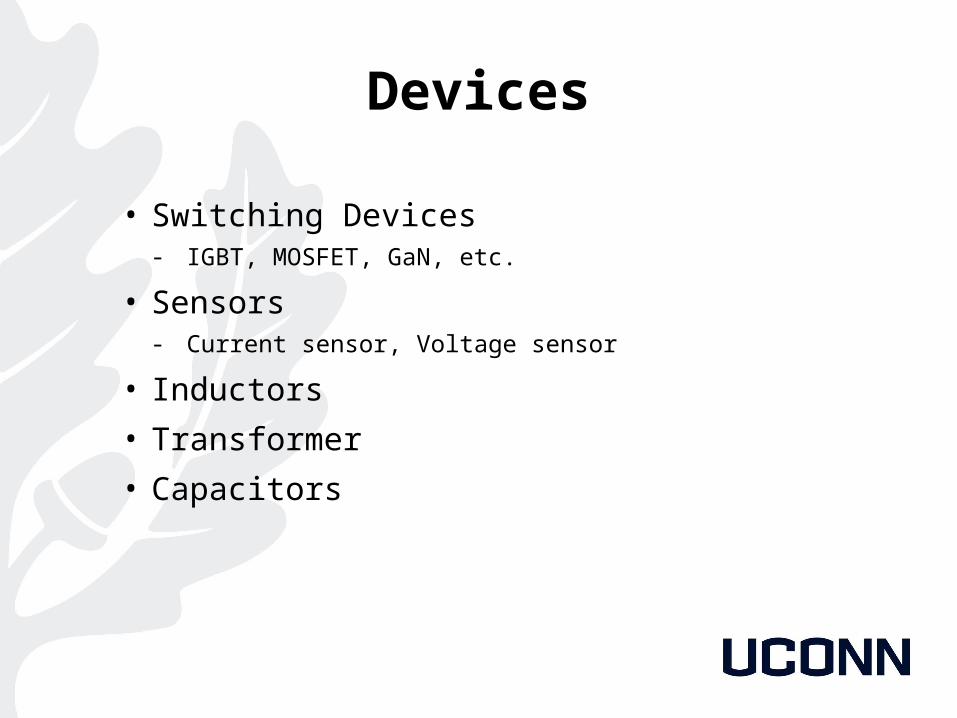
Devices
• Switching Devices - IGBT, MOSFET, GaN, etc.
• Sensors - Current sensor, Voltage sensor
• Inductors• Transformer • Capacitors
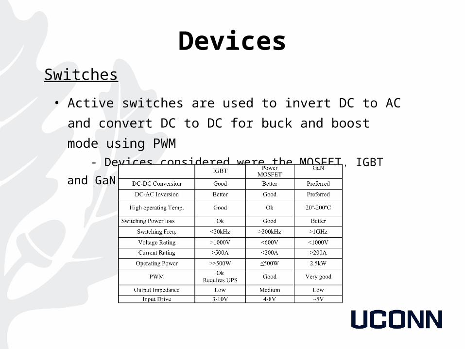
Devices
• Active switches are used to invert DC to AC and convert DC to
DC for buck and boost mode using PWM - Devices considered were the MOSFET, IGBT and GaN
Switches
• The device of choice is the Power MOSFET- High switching frequency ( >200kHZ)
o Reduces the size of the passive elements i.e.
Inductors, Capacitors
- Low switching power loss- Low conduction resistance- Low cost
DevicesSwitches
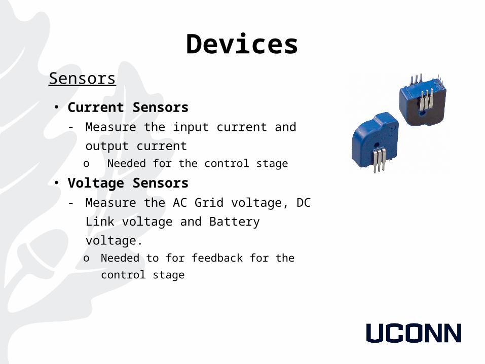
DevicesSensors
• Current Sensors - Measure the input current and output current
o Needed for the control stage
• Voltage Sensors - Measure the AC Grid voltage, DC Link voltage
and Battery voltage.o Needed to for feedback for the control stage
PCB BoardUsing Altium Designer software, we plan on designing our
PCB board using the Top and Bottom layer for the components, as well as a mid-layers for common connections, reduce noise levels, and for High Current usage. (Power, Ground, etc.)
When building a PCB board, there are different things to consider for the most efficient, safest and reliable Power usage.
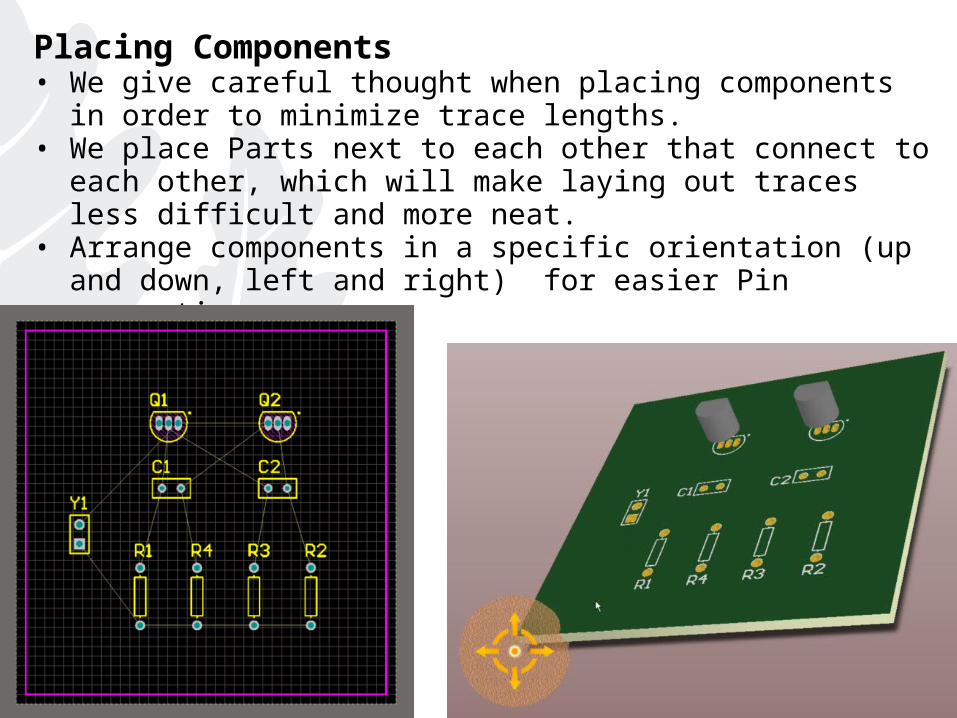
Placing Components• We give careful thought when placing components in order to minimize
trace lengths.• We place Parts next to each other that connect to each other, which will
make laying out traces less difficult and more neat.• Arrange components in a specific orientation (up and down, left and
right) for easier Pin connections.
Using complete planes for Power, Ground, etc.
Copper pours on signal layers are common in PCB’s:
• Can be a hatched ground pour an analog design
• Solid Power supply pour for carrying heavy currents
• Solid ground pour for EMC shielding
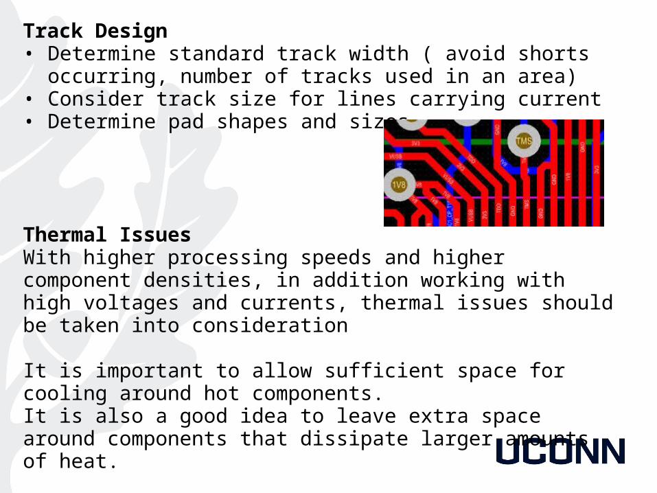
Track Design• Determine standard track width ( avoid shorts occurring, number of
tracks used in an area)• Consider track size for lines carrying current• Determine pad shapes and sizes
Thermal IssuesWith higher processing speeds and higher component densities, in addition working with high voltages and currents, thermal issues should be taken into consideration
It is important to allow sufficient space for cooling around hot components.It is also a good idea to leave extra space around components that dissipate larger amounts of heat.
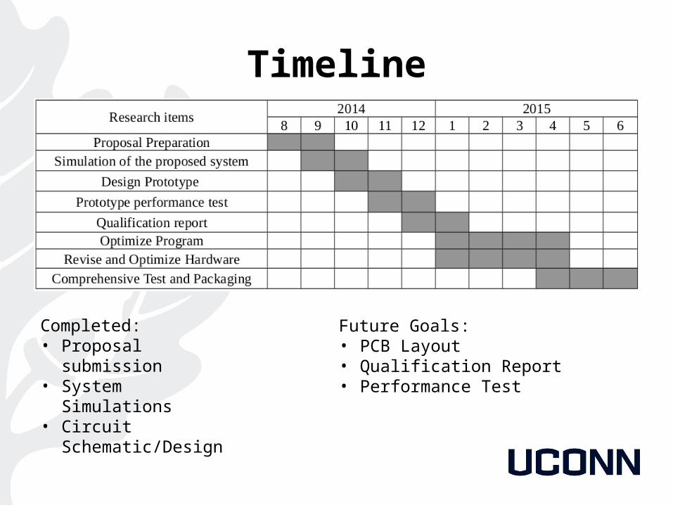
Timeline
Completed:• Proposal submission• System Simulations• Circuit Schematic/Design
Future Goals:• PCB Layout• Qualification Report• Performance Test
Timeline
Completed:• Proposal submission• System Simulations• Circuit Schematic/Design
Future Goals:• PCB Layout• Qualification Report• Performance Test