1. Product profile 1.1 General description High-speed switching diodes, encapsulated in small Surface-Mounted Device (SMD) plastic packages. 1.2 Features and benefits 1.3 Applications 1.4 Quick reference data [1] When switched from I F = 10 mA to I R = 10 mA; R L = 100 Ω; measured at I R = 1 mA. BAV99 series High-speed switching diodes Rev. 8 — 18 November 2010 Product data sheet Table 1. Product overview Type number Package Configuration Package configuration Nexperia JEITA JEDEC BAV99 SOT23 - TO-236AB dual series small BAV99S SOT363 SC-88 - quadruple; 2 series very small BAV99W SOT323 SC-70 - dual series very small High switching speed: t rr ≤ 4 ns Low capacitance: C d ≤ 1.5 pF Low leakage current Reverse voltage: V R ≤ 100 V Small SMD plastic packages AEC-Q101 qualified High-speed switching Reverse polarity protection General-purpose switching Table 2. Quick reference data Symbol Parameter Conditions Min Typ Max Unit Per diode I R reverse current V R = 80 V - - 0.5 μA V R reverse voltage - - 100 V t rr reverse recovery time [1] - - 4 ns
Transcript
1. Product profile
1.1 General descriptionHigh-speed switching diodes, encapsulated in small Surface-Mounted Device (SMD) plastic packages.
1.2 Features and benefits
1.3 Applications
1.4 Quick reference data
[1] When switched from IF = 10 mA to IR = 10 mA; RL = 100 Ω; measured at IR = 1 mA.
BAV99 seriesHigh-speed switching diodesRev. 8 — 18 November 2010 Product data sheet
Table 1. Product overviewType number Package Configuration Package
configurationNexperia JEITA JEDECBAV99 SOT23 - TO-236AB dual series small
BAV99S SOT363 SC-88 - quadruple; 2 series very small
BAV99W SOT323 SC-70 - dual series very small
High switching speed: trr ≤ 4 ns Low capacitance: Cd ≤ 1.5 pFLow leakage current Reverse voltage: VR ≤ 100 VSmall SMD plastic packages AEC-Q101 qualified
Product data sheet Rev. 8 — 18 November 2010 5 of 14
Nexperia BAV99 seriesHigh-speed switching diodes
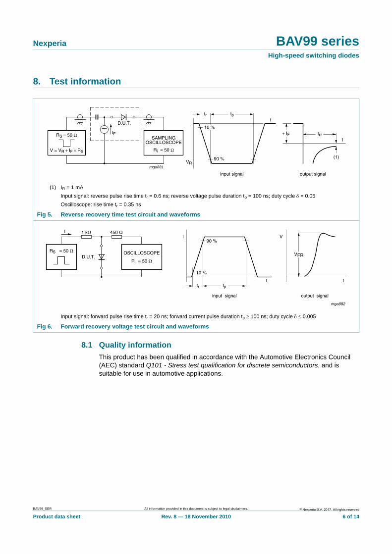
8. Test information
8.1 Quality informationThis product has been qualified in accordance with the Automotive Electronics Council (AEC) standard Q101 - Stress test qualification for discrete semiconductors, and is suitable for use in automotive applications.
(1) IR = 1 mAInput signal: reverse pulse rise time tr = 0.6 ns; reverse voltage pulse duration tp = 100 ns; duty cycle δ = 0.05Oscilloscope: rise time tr = 0.35 ns
Fig 5. Reverse recovery time test circuit and waveforms
Product data sheet Rev. 8 — 18 November 2010 11 of 14
Nexperia BAV99 seriesHigh-speed switching diodes
13. Legal information
13.1 Data sheet status
[1] Please consult the most recently issued document before initiating or completing a design.
[2] The term ‘short data sheet’ is explained in section “Definitions”.
[3] The product status of device(s) described in this document may have changed since this document was published and may differ in case of multiple devices. The latest product status information is available on the Internet at URL http://www.nexperia.com.
13.2 DefinitionsDraft — The document is a draft version only. The content is still under internal review and subject to formal approval, which may result in modifications or additions. Nexperia does not give any representations or warranties as to the accuracy or completeness of information included herein and shall have no liability for the consequences of use of such information.
Short data sheet — A short data sheet is an extract from a full data sheet with the same product type number(s) and title. A short data sheet is intended for quick reference only and should not be relied upon to contain detailed and full information. For detailed and full information see the relevant full data sheet, which is available on request via the local Nexperia sales office. In case of any inconsistency or conflict with the short data sheet, the full data sheet shall prevail.
Product specification — The information and data provided in a Product data sheet shall define the specification of the product as agreed between Nexperia and its customer, unless Nexperia and customer have explicitly agreed otherwise in writing. In no event however, shall an agreement be valid in which the Nexperia product is deemed to offer functions and qualities beyond those described in the Product data sheet.
13.3 DisclaimersLimited warranty and liability — Information in this document is believed to be accurate and reliable. However, Nexperia does not give any representations or warranties, expressed or implied, as to the accuracy or completeness of such information and shall have no liability for the consequences of use of such information.
In no event shall Nexperia be liable for any indirect, incidental, punitive, special or consequential damages (including - without limitation - lost profits, lost savings, business interruption, costs related to the removal or replacement of any products or rework charges) whether or not such damages are based on tort (including negligence), warranty, breach of contract or any other legal theory.
Notwithstanding any damages that customer might incur for any reason whatsoever, Nexperia’s aggregate and cumulative liability towards customer for the products described herein shall be limited in accordance with the Terms and conditions of commercial sale of Nexperia.
Right to make changes — Nexperia reserves the right to make changes to information published in this document, including without limitation specifications and product descriptions, at any time and without notice. This document supersedes and replaces all information supplied prior to the publication hereof.
Suitability for use — Nexperia products are not designed, authorized or warranted to be suitable for use in life support, life-critical or safety-critical systems or equipment, nor in applications where failure or
malfunction of a Nexperia product can reasonably be expected to result in personal injury, death or severe property or environmental damage. Nexperia accepts no liability for inclusion and/or use of Nexperia products in such equipment or applications and therefore such inclusion and/or use is at the customer’s own risk.
Applications — Applications that are described herein for any of these products are for illustrative purposes only. Nexperia makes no representation or warranty that such applications will be suitable for the specified use without further testing or modification.
Customers are responsible for the design and operation of their applications and products using Nexperia products, and Nexperia accepts no liability for any assistance with applications or customer product design. It is customer’s sole responsibility to determine whether the Nexperia product is suitable and fit for the customer’s applications and products planned, as well as for the planned application and use of customer’s third party customer(s). Customers should provide appropriate design and operating safeguards to minimize the risks associated with their applications and products.
Nexperia does not accept any liability related to any default, damage, costs or problem which is based on any weakness or default in the customer’s applications or products, or the application or use by customer’s third party customer(s). Customer is responsible for doing all necessary testing for the customer’s applications and products using Nexperia products in order to avoid a default of the applications and the products or of the application or use by customer’s third party customer(s). Nexperia does not accept any liability in this respect.
Limiting values — Stress above one or more limiting values (as defined in the Absolute Maximum Ratings System of IEC 60134) will cause permanent damage to the device. Limiting values are stress ratings only and (proper) operation of the device at these or any other conditions above those given in the Recommended operating conditions section (if present) or the Characteristics sections of this document is not warranted. Constant or repeated exposure to limiting values will permanently and irreversibly affect the quality and reliability of the device.
Terms and conditions of commercial sale — Nexperia products are sold subject to the general terms and conditions of commercial sale, as published at http://www.nexperia.com/profile/terms, unless otherwise agreed in a valid written individual agreement. In case an individual agreement is concluded only the terms and conditions of the respective agreement shall apply. Nexperia hereby expressly objects to applying the customer’s general terms and conditions with regard to the purchase of Nexperia products by customer.
No offer to sell or license — Nothing in this document may be interpreted or construed as an offer to sell products that is open for acceptance or the grant, conveyance or implication of any license under any copyrights, patents or other industrial or intellectual property rights.
Export control — This document as well as the item(s) described herein may be subject to export control regulations. Export might require a prior authorization from national authorities.
Quick reference data — The Quick reference data is an extract of the product data given in the Limiting values and Characteristics sections of this document, and as such is not complete, exhaustive or legally binding.
13.4 TrademarksNotice: All referenced brands, product names, service names and trademarks are the property of their respective owners.
14. Contact information
For more information, please visit: http://www.nexperia.com
For sales office addresses, please send an email to: [email protected]