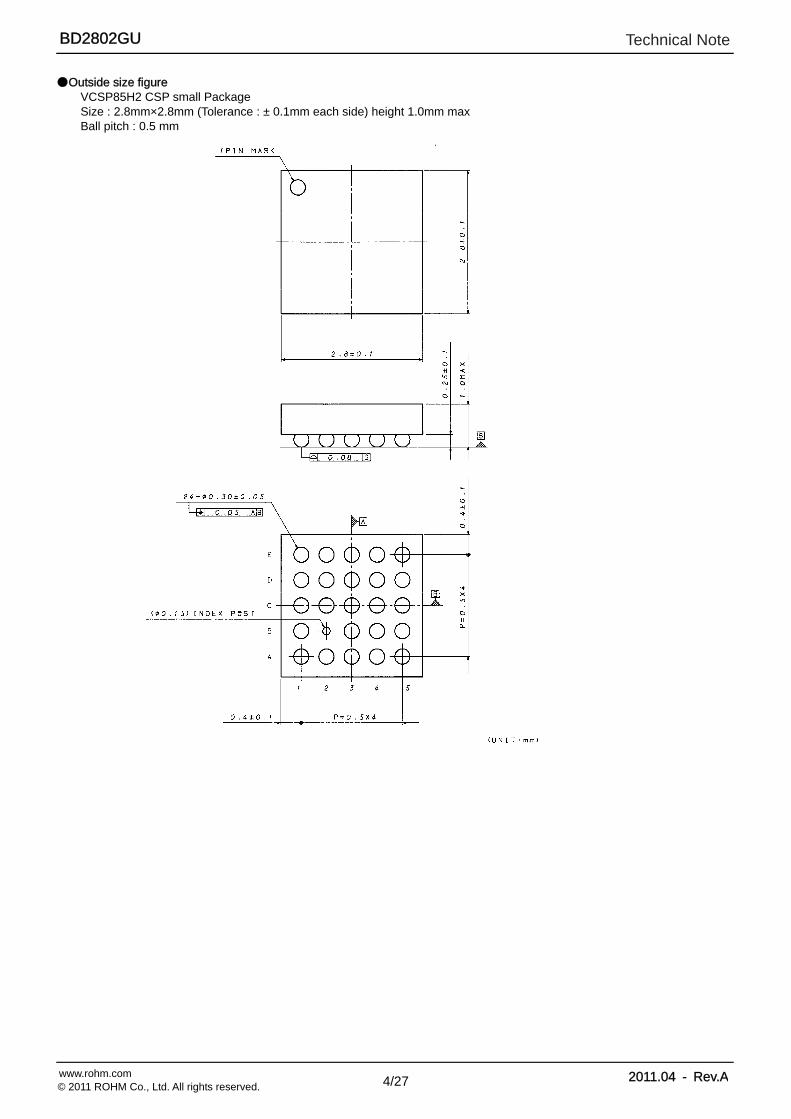
The BD2802GU is a RGB LED driver specifically engineered for decoration purposes.This RGB driver incorporates lighting patterns and illuminates without imposing any load on CPU.This RGB driver is best-suited for illumination using RGB LEDs and decoration using monochrome LEDs.In addition, this RGB driver has been successfully miniaturized through the use of a VCSP85H2 (2.8 mm 0.5 mm pitch) chip size package.
Features
1) RGB LED driver (dual drivers) - A slope control function is incorporated (allowing dual drivers to be controlled independently). - Slope control can be implemented using the DC current. - Two modes “continuous illumination mode” and “illumination single cycle mode” are supported. - Independent external ON/OFF synchronizing terminals (of dual drivers) are provided. - Multiple drivers can be used concurrently by using the I2C address change function and supporting reference clock I/O. 2) Thermal shutdown 3) I2C BUS fast mode support (maximum rate: 400 kHz) - A device address can be changed via an external pin.
* This driver has not been designed for anti-radiation. * This document may be altered without prior notice. * This document does not provide for delivery.
Absolute Maximum Ratings(Ta=25)
Parameter Symbol Limits Unit
Maximum Applied voltage VMAX 7 V
Power Dissipation Pd 1250 (Note1) mW
Operating Temperature Range Topr -40 ~ +85
Storage Temperature Range Tstg -55 ~ +150
(Note1)Power dissipation deleting is 10.0mW/ oC, when it’s used in over 25 oC. (It’s deleting is on the board that is ROHM’s standard)
I2C BUS format The writing operation is based on the I2C slave standard.
・Slave address
A7 A6 A5 A4 A3 A2 A1 R/W
ADDSEL=L 0 0 1 1 0 1 0 0
ADDSEL=H 0 0 1 1 0 1 1 0
Slave address can be changed with the external terminal ADDSEL. ・Bit Transfer
SCL transfers 1-bit data during H. SCL cannot change signal of SDA during H at the time of bit transfer. If SDA changes while SCL is H, START conditions or STOP conditions will occur and it will be interpreted as a control signal.
SDA
SCL
SDA a state of stability:Data are effective
SDA It can change
・START and STOP condition
When SDA and SCL are H, data is not transferred on the I2C- bus. This condition indicates, if SDA changes from H to L while SCL has been H, it will become START (S) conditions, and an access start, if SDA changes from L to H while SCL has been H, it will become STOP (P) conditions and an access end.
SDA
SCL S P
START condition STOP condition
・Acknowledge
It transfers data 8 bits each after the occurrence of START condition. A transmitter opens SDA after transfer 8bits data, and a receiver returns the acknowledge signal by setting SDA to L.
・Writing protocol A register address is transferred by the next 1 byte that transferred the slave address and the write-in command. The 3rd byte writes data in the internal register written in by the 2nd byte, and after 4th byte or, the increment of register address is carried out automatically. However, when a register address turns into the last address, it is set to 00h by the next transmission. After the transmission end, the increment of the address is carried out.
S A A A P
register addressslave address
from master to slave
from slave to master
R/W=0(write)
DATA
AD7 D6 D5 D4 D3 D2 D1 D0 D7 D6 D5 D4 D3 D2 D1 D0 A7 A6 A5 A4 A3 A2 A1 A00 X X X X X X X
* RGB*OS returns to 0 automatically after 1 cycle operation. * RGB*EN precedes to RGB*OS. In use in 1 cycle operation, there is the necessity for RGB*EN=0.
Adress 02h <RGB1 time>
BIT Name Init Function
0 1
D7 SFRGB1(1) 0 SFRGB1(1) SFRGB1(0) Slope Down transition
0 0 0 0 1 Wave form cycle / 16 1 0 Wave form cycle / 8 1 1 Wave form cycle / 4
It is a theoretical value on logic control, and the reaction time of the analog section is not included."Slope time" is the time from a slope start to a slope end.
D6 SFRGB1(0) 0
D5 SRRGB1(1) 0 SRRGB1(1) SRRGB1(0) Slope Up transition
0 0 0 0 1 Wave form cycle / 16 1 0 Wave form cycle / 8 1 1 Wave form cycle / 4
It is a theoretical value on logic control, and the reaction time of the analog section is not included."Slope time" is the time from a slope start to a slope end.
D4 SRRGB1(0) 0
D3 - - - -
D2 TRGB1(2) 0 TRGB1(2) TRGB1(1) TRGB1(0) Wave form cycle
0 0 0 0.131 s 0 0 1 0.52 s 0 1 0 1.05 s 0 1 1 2.10 s 1 0 0 4.19 s 1 0 1 8.39 s 1 1 0 12.6 s 1 1 1 16.8 s
D1 TRGB1(1) 0
D0 TRGB1(0) 0
Setting time is counted based on the frequency of OSC. The above-mentioned value is a value at the time of Typ (1MHz). When operating by the external clock, input frequency is a value at the time of Typ (250kHz). *Refer to "Use of a RGB wave setup " for the detailed function of each register of this page.
D7 SFRGB2(1) 0 SFRGB2(1) SFRGB2(0) Slope Down transition
0 0 0 0 1 Wave form cycle / 16 1 0 Wave form cycle / 8 1 1 Wave form cycle / 4
It is a theoretical value on logic control, and the reaction time of the analog section is not included. "Slope time" is the time from a slope start to a slope end.
D6 SFRGB2(0) 0
D5 SRRGB2(1) 0
SRRGB2(1) SRRGB2(0) Slope up transition 0 0 0 0 1 Wave form cycle / 16 1 0 Wave form cycle / 8 1 1 Wave form cycle / 4
It is a theoretical value on logic control, and the reaction time of the analog section is not
included. "Slope time" is the time from a slope start to a slope end.
D4 SRRGB2(0) 0
D3 - - - -
D2 TRGB2(2) 0 TRGB2(2) TRGB2(1) TRGB2(0) Wave form cycle
0 0 0 0.131 s 0 0 1 0.52 s 0 1 0 1.05 s 0 1 1 2.10 s 1 0 0 4.19 s 1 0 1 8.39 s 1 1 0 12.6 s 1 1 1 16.8 s
D1 TRGB2(1) 0
D0 TRGB2(0) 0
Setting time is counted based on the frequency of OSC. The above-mentioned value is a value at the time of Typ (1MHz). When operating by the external clock, input frequency is a value at the time of Typ (250kHz) *Refer to "Use of a RGB wave setup " for the detailed function of each register of this page.
RGB LED Driver Operation Description - Two drivers “RGB1 (R1LED, G1LED, B1LED)” and “RGB2 (R2LED, G2LED, B2LED)” are mounted. - A slope function is incorporated to control drivers independently. - Refer to RGB Waveform Setting for more information about output waveform setting. - The LED current can be set via a resistance value (RISET) to be connected to the RGBISET terminal. The maximum
current value can be derived from the following expression: ILEDmax [A] = 3.048 / RISET [kΩ] (Typ)
However, this setting must be made so that the maximum current value can be less than or equal to 30.48mA. In addition, the RGBISET terminal has an overcurrent protection circuit to prevent the excessive LED current from flowing for low impedance to the ground.
- Note that the setting voltage shall be higher than or equal to a saturation voltage (0.2V) in the constant current circuit. When LED Vf is large, the LED destination shall be connected to another step-up circuit.
- The LED destination is fixed before on (RGB*EN=Hi or RGB*OS=Hi).
VLED
RGB*EN Or
RGB*OS
VLED
RGB*ENOr
RGB*OS
The synchronism of RGB1/RGB2
The period of RGB1 and RGB2 and start, stop timing can be set up independently. When synchronizes RGB1 and RGB2, You must start an internal counter at the same time under the state of resetting. (Internal Counter are prepared for each of RGB1 and RGB2, so You must reset both.) <How to reset internal Counter> Inside Counter can be reset by carrying out one of following actions.
• Reset by hard reset (RSTB_IL). (RGB1, RGB2 is reset together.) • Reset by soft reset. (RGB1, RGB2 is reset together.) • It is written register of the current setup (I1・I2), the slope setup, the period setup and the pattern setup.
Internal Counter of RGB1 is reset when it is written between Address=0Bh from 02h. Internal Counter of RGB2 is reset when it is written between Address=15h from 0Ch. Counter is reset as to overwriting the same value.
Note)
Internal Counter isn't reset if write RGB1EN =L and RGB2EN =L. (Address=01h). When it write RGB1EN=L (RGB2EN=L), inside Counter is held, and IC will operate from the held state at next restart.
RGB Waveform Setting Various kinds of RGB control can be implemented by designating waveform cycles, waveform patterns, current settings 1, 2 and rising/falling slope times. To activate a RGB waveform, a continuous operation via RGB*EN or a single-shot operation via RGB*OS can be selected. In addition, when control via the external terminal RGB*CNT is enabled via RGB*MEL, the corresponding LED can be lit in synchronization with the external signal.
1. Waveform cycle
A single cycle time is set for a waveform pattern. This setting can be made independently for RGB1 and RGB2.
2. Waveform pattern A pattern in a waveform cycle is set. Sixteen types of waveform patterns can be set in units of waveform patterns. For concrete waveform patterns, refer to the timing diagram shown on the next page.
3. Current settings 1 and 2 (I1, I2) Two currents in a waveform pattern are set. When the maximum current value is 25.4mA, it is possible to set the current ranging from 0 to 25.4mA with an
increment of 0.2mA (128 steps). The polarity of a waveform is determined by the greater-than/ less-than relationship in the current setting. This setting can be made in units of terminals.
4. Rising/falling slope time A current change time during switching between current settings 1 and 2 is set. A time per step (0.2mA) is calculated based on a difference between the currents selected in current settings 1, 2
and a setting slope time. For this reason, a time per step (0.2mA) is short when a difference between setting currents I1 and I2 is large. In
contrast, it is long when a difference between setting currents I1 and I2 is small. Regardless of current settings 1 and 2, a rising slope time applies at current increase and a falling slope time applies
at current decrease. For concrete waveform images, refer to the timing diagram shown on the next page. 5. External terminal synchronization control
When control via the external terminal RGB*CNT is enabled via RGB*MEL, lighting is enabled if the input external signal goes “H.” In contrast, it is disabled if the external input signal goes “L.” In this way, synchronization with the external signal is enabled so that LED can be blinked in conjunction with a ringing tone (a melody signaling a ringtone).
RGB*CNT
RGB*MEL
B*LED
G*LED
R*LED
External terminal control is enabled.
External terminal control is disabled.
Remains “Enabled” with RGB*MEL=1 and
RGB*CNT=H
A RGB thin line indicates an image where external terminal control does not take place.
6. Clock I/O A reference clock I/O function is mounted in this IC chip. When two IC chips are used to extend an illumination capability, clock supply to the other RGB LED driver can be accomplished for synchronization with this LSI chip. This setting can be made via the register. Clock output can be made with CLKEN=1 and CLKMD=1.
Register CLKIO terminal state Clock reception
CLKEN CLKMD
0 0/1 Input Does not receive external clocks.
1 0 Input Operates on external clocks. 1 Output -
Wave cycle
Wave pattern 1 (00h)
Current 1(I1)
Current 2(I2)
Slope uptransition
Slope Down transition
(ex)The image of current change of Wave pattern 11
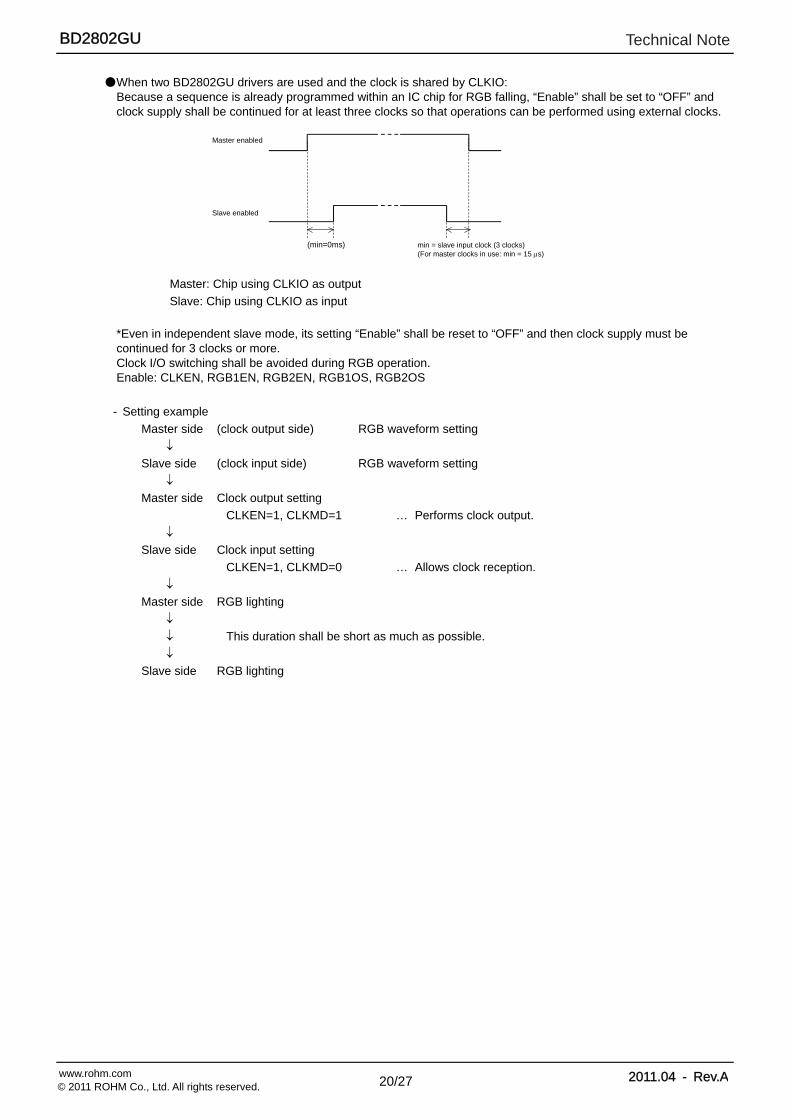
When two BD2802GU drivers are used and the clock is shared by CLKIO: Because a sequence is already programmed within an IC chip for RGB falling, “Enable” shall be set to “OFF” and clock supply shall be continued for at least three clocks so that operations can be performed using external clocks.
Master: Chip using CLKIO as output
Slave: Chip using CLKIO as input
*Even in independent slave mode, its setting “Enable” shall be reset to “OFF” and then clock supply must be continued for 3 clocks or more. Clock I/O switching shall be avoided during RGB operation. Enable: CLKEN, RGB1EN, RGB2EN, RGB1OS, RGB2OS
- Setting example
Master side (clock output side) RGB waveform setting
Slave side (clock input side) RGB waveform setting
Setting a rising/falling slope time to “0” causes blinkingto take place. Phase switching takes place via the setting currents of R and G.
This example shows that lighting occurs continuously in the order of white, red, red and red. To achieve this, waveform patterns 16, 1 and RGB*OS single cycle operation need to be combined.
[Example 2] Blinking Waveform cycle [Example 5] Continuous lighting of four LEDs
Waveform cycle
When a rising/falling slope time is longer than the setting made in example 2, a continuous color changeis made by slope operation.
R, G and B waveform patterns are set in a way that anyof R, G and B changes constantly.
There are two types of reset: software reset and hardware reset. (1) Software reset
- Setting the register (SFTRST) to “1” causes all the registers to be initialized. - The registers subject to software reset automatically return to zero (Auto Return 0).
(2) Hardware reset - Changing the RESETB terminal setting from “H” to “L” causes a state subject to hardware reset. - Attempting hardware reset causes the states of all registers and output terminals to be initialized to their initial
values, so that address reception is entirely stopped. - Attempting reset in the hardware reset state causes the RESETB terminal state to change from “L” to “H” and vice versa. - The RESETB terminal is provided with a filter circuit and a duration of 5µs or less with the terminal set to “L” is not
recognized as hardware reset. (3) Reset sequence
- When hardware reset is attempted during software reset, software reset is already cleared when hardware reset is cleared (because the software reset initial value is 0).
2. Thermal shutdown
The thermal shutdown is effective for LED and OSC portions. The thermal shutdown function is activated when the detected temperature is approx. 195C. The detected temperature has a hysteresis and the detection cancel temperature is approx. 175C (reference value in design).
3. I/O portion
While the RESETB terminal is in “L” state, no input signal is propagated to the IC logic portion because SDA and SCL input buffer operations are all stopped.
Level shifter
Logic
When RESETB=L, output is fixed at “H.”
EN
SCL (SDA)
RESETB
Special care should be taken because a current path may be formed via a terminal protection diode, depending on an I/O power-on sequence or an input level.
4. Power on/off sequence
Voltage shall be applied as follows at driver activation. When a delay element is connected to a VIO voltage source and a reset cancel signal is input to the RESETB terminal, special care should be taken to the rising time of VIO voltage to delay the RESETB signal without fail.
5. Terminating the unused terminals Be sure to set the test terminals and unused terminals as summarized in the following table.In addition, refer to the preceding equivalent circuit and terminate the above terminals in a way that no problem occurs during actual use.
T1, T2, T3, T4 Test input terminals. Short-circuit these terminals to GND.
LED terminals not to be used Short-circuit these terminals to GND. In this case, don’t set the registers related to LEDs not to be used.
RGB1CNT, RGB2CNT Short-circuit these terminals to GND.(Built-in pull-down resistance) CLKIO Short-circuit this terminal to GND.(Built-in pull-down resistance) ADDSEL Be sure to short-circuit this terminal to VBAT or GND.
VIO
RESETB
VBAT
TVBATOFF
TRSTB=min 0.1ms
TRST=min 0.1ms
不 可 レジスタ制御 可 能 不 可
TACSS=min 0.1ms
Register control Register control disabled Register control enabled Register control disabled
An excess in the absolute maximum ratings, such as supply voltage, temperature range of operating conditions, etc., can break down devices, thus making impossible to identify breaking mode such as a short circuit or an open circuit. If any special mode exceeding the absolute maximum ratings is assumed, consideration should be given to take physical safety measures including the use of fuses, etc.
(2) Power supply and ground line Design PCB pattern to provide low impedance for the wiring between the power supply and the ground lines. Pay attention to the interference by common impedance of layout pattern when there are plural power supplies and ground lines. Especially, when there are ground pattern for small signal and ground pattern for large current included the external circuits, please separate each ground pattern. Furthermore, for all power supply pins to ICs, mount a capacitor between the power supply and the ground pin. At the same time, in order to use a capacitor, thoroughly check to be sure the characteristics of the capacitor to be used present no problem including the occurrence of capacity dropout at a low temperature, thus determining the constant.
(3) Ground voltage Make setting of the potential of the ground pin so that it will be maintained at the minimum in any operating state. Furthermore, check to be sure no pins are at a potential lower than the ground voltage including an actual electric transient.
(4) Short circuit between pins and erroneous mounting In order to mount ICs on a set PCB, pay thorough attention to the direction and offset of the ICs. Erroneous mounting can break down the ICs. Furthermore, if a short circuit occurs due to foreign matters entering between pins or between the pin and the power supply or the ground pin, the ICs can break down.
(5) Operation in strong electromagnetic field Be noted that using ICs in the strong electromagnetic field can malfunction them.
(6) Input pins In terms of the construction of IC, parasitic elements are inevitably formed in relation to potential. The operation of the parasitic element can cause interference with circuit operation, thus resulting in a malfunction and then breakdown of the input pin. Therefore, pay thorough attention not to handle the input pins, such as to apply to the input pins a voltage lower than the ground respectively, so that any parasitic element will operate. Furthermore, do not apply a voltage to the input pins when no power supply voltage is applied to the IC. In addition, even if the power supply voltage is applied, apply to the input pins a voltage lower than the power supply voltage or within the guaranteed value of electrical characteristics.
(7) External capacitor In order to use a ceramic capacitor as the external capacitor, determine the constant with consideration given to a degradation in the nominal capacitance due to DC bias and changes in the capacitance due to temperature, etc.
(8) Thermal shutdown circuit (TSD) This LSI builds in a thermal shutdown (TSD) circuit. When junction temperatures become detection temperature or higher, the thermal shutdown circuit operates and turns a switch OFF. The thermal shutdown circuit, which is aimed at isolating the LSI from thermal runaway as much as possible, is not aimed at the protection or guarantee of the LSI. Therefore, do not continuously use the LSI with this circuit operating or use the LSI assuming its operation.
(9) Thermal design Perform thermal design in which there are adequate margins by taking into account the permissible dissipation (Pd) in actual states of use.
(10) About the pin for the test, the un-use pin Prevent a problem from being in the pin for the test and the un-use pin under the state of actual use. Please refer to a function manual and an application notebook. And, as for the pin that doesn't specially have an explanation, ask our company person in charge.
(11) About the rush current Because the rush current flows momentarily for internal logic instability caused by a power-on sequence or delay, special care should be taken to the power supply coupling capacity, power supply, ground pattern wiring width and wiring.
(12) About descriptions given in this document Though the function description and application node are design documents prepared for application design, we don’t take liability for descriptions given in these documents. Be sure to decide applications after thoroughly investigating and evaluating the external devices as well as this BS2802GU LED driver.
1. Our Products are designed and manufactured for application in ordinary electronic equipments (such as AV equipment, OA equipment, telecommunication equipment, home electronic appliances, amusement equipment, etc.). If you intend to use our Products in devices requiring extremely high reliability (such as medical equipment (Note 1), transport equipment, traffic equipment, aircraft/spacecraft, nuclear power controllers, fuel controllers, car equipment including car accessories, safety devices, etc.) and whose malfunction or failure may cause loss of human life, bodily injury or serious damage to property (“Specific Applications”), please consult with the ROHM sales representative in advance. Unless otherwise agreed in writing by ROHM in advance, ROHM shall not be in any way responsible or liable for any damages, expenses or losses incurred by you or third parties arising from the use of any ROHM’s Products for Specific Applications.
(Note1) Medical Equipment Classification of the Specific Applications JAPAN USA EU CHINA
CLASSⅢ CLASSⅢ
CLASSⅡb CLASSⅢ
CLASSⅣ CLASSⅢ
2. ROHM designs and manufactures its Products subject to strict quality control system. However, semiconductor
products can fail or malfunction at a certain rate. Please be sure to implement, at your own responsibilities, adequate safety measures including but not limited to fail-safe design against the physical injury, damage to any property, which a failure or malfunction of our Products may cause. The following are examples of safety measures:
[a] Installation of protection circuits or other protective devices to improve system safety [b] Installation of redundant circuits to reduce the impact of single or multiple circuit failure
3. Our Products are designed and manufactured for use under standard conditions and not under any special or extraordinary environments or conditions, as exemplified below. Accordingly, ROHM shall not be in any way responsible or liable for any damages, expenses or losses arising from the use of any ROHM’s Products under any special or extraordinary environments or conditions. If you intend to use our Products under any special or extraordinary environments or conditions (as exemplified below), your independent verification and confirmation of product performance, reliability, etc, prior to use, must be necessary:
[a] Use of our Products in any types of liquid, including water, oils, chemicals, and organic solvents [b] Use of our Products outdoors or in places where the Products are exposed to direct sunlight or dust [c] Use of our Products in places where the Products are exposed to sea wind or corrosive gases, including Cl2,
H2S, NH3, SO2, and NO2
[d] Use of our Products in places where the Products are exposed to static electricity or electromagnetic waves [e] Use of our Products in proximity to heat-producing components, plastic cords, or other flammable items [f] Sealing or coating our Products with resin or other coating materials [g] Use of our Products without cleaning residue of flux (even if you use no-clean type fluxes, cleaning residue of
flux is recommended); or Washing our Products by using water or water-soluble cleaning agents for cleaning residue after soldering
[h] Use of the Products in places subject to dew condensation
4. The Products are not subject to radiation-proof design. 5. Please verify and confirm characteristics of the final or mounted products in using the Products. 6. In particular, if a transient load (a large amount of load applied in a short period of time, such as pulse. is applied,
confirmation of performance characteristics after on-board mounting is strongly recommended. Avoid applying power exceeding normal rated power; exceeding the power rating under steady-state loading condition may negatively affect product performance and reliability.
7. De-rate Power Dissipation (Pd) depending on Ambient temperature (Ta). When used in sealed area, confirm the actual
ambient temperature. 8. Confirm that operation temperature is within the specified range described in the product specification. 9. ROHM shall not be in any way responsible or liable for failure induced under deviant condition from what is defined in
this document.
Precaution for Mounting / Circuit board design 1. When a highly active halogenous (chlorine, bromine, etc.) flux is used, the residue of flux may negatively affect product
performance and reliability. 2. In principle, the reflow soldering method must be used; if flow soldering method is preferred, please consult with the
ROHM representative in advance. For details, please refer to ROHM Mounting specification
Precautions Regarding Application Examples and External Circuits 1. If change is made to the constant of an external circuit, please allow a sufficient margin considering variations of the
characteristics of the Products and external components, including transient characteristics, as well as static characteristics.
2. You agree that application notes, reference designs, and associated data and information contained in this document
are presented only as guidance for Products use. Therefore, in case you use such information, you are solely responsible for it and you must exercise your own independent verification and judgment in the use of such information contained in this document. ROHM shall not be in any way responsible or liable for any damages, expenses or losses incurred by you or third parties arising from the use of such information.
Precaution for Electrostatic
This Product is electrostatic sensitive product, which may be damaged due to electrostatic discharge. Please take proper caution in your manufacturing process and storage so that voltage exceeding the Products maximum rating will not be applied to Products. Please take special care under dry condition (e.g. Grounding of human body / equipment / solder iron, isolation from charged objects, setting of Ionizer, friction prevention and temperature / humidity control).
Precaution for Storage / Transportation 1. Product performance and soldered connections may deteriorate if the Products are stored in the places where:
[a] the Products are exposed to sea winds or corrosive gases, including Cl2, H2S, NH3, SO2, and NO2 [b] the temperature or humidity exceeds those recommended by ROHM [c] the Products are exposed to direct sunshine or condensation [d] the Products are exposed to high Electrostatic
2. Even under ROHM recommended storage condition, solderability of products out of recommended storage time period may be degraded. It is strongly recommended to confirm solderability before using Products of which storage time is exceeding the recommended storage time period.
3. Store / transport cartons in the correct direction, which is indicated on a carton with a symbol. Otherwise bent leads
may occur due to excessive stress applied when dropping of a carton. 4. Use Products within the specified time after opening a humidity barrier bag. Baking is required before using Products of
which storage time is exceeding the recommended storage time period.
Precaution for Product Label QR code printed on ROHM Products label is for ROHM’s internal use only.
Precaution for Disposition When disposing Products please dispose them properly using an authorized industry waste company.
Precaution for Foreign Exchange and Foreign Trade act Since our Products might fall under controlled goods prescribed by the applicable foreign exchange and foreign trade act, please consult with ROHM representative in case of export.
Precaution Regarding Intellectual Property Rights 1. All information and data including but not limited to application example contained in this document is for reference
only. ROHM does not warrant that foregoing information or data will not infringe any intellectual property rights or any other rights of any third party regarding such information or data. ROHM shall not be in any way responsible or liable for infringement of any intellectual property rights or other damages arising from use of such information or data.:
2. No license, expressly or implied, is granted hereby under any intellectual property rights or other rights of ROHM or any
third parties with respect to the information contained in this document.
Other Precaution 1. This document may not be reprinted or reproduced, in whole or in part, without prior written consent of ROHM. 2. The Products may not be disassembled, converted, modified, reproduced or otherwise changed without prior written
consent of ROHM. 3. In no event shall you use in any way whatsoever the Products and the related technical information contained in the
Products or this document for any military purposes, including but not limited to, the development of mass-destruction weapons.
4. The proper names of companies or products described in this document are trademarks or registered trademarks of
General Precaution 1. Before you use our Pro ducts, you are requested to care fully read this document and fully understand its contents.
ROHM shall n ot be in an y way responsible or liabl e for fa ilure, malfunction or acci dent arising from the use of a ny ROHM’s Products against warning, caution or note contained in this document.
2. All information contained in this docume nt is current as of the issuing date and subj ect to change without any prior
notice. Before purchasing or using ROHM’s Products, please confirm the la test information with a ROHM sale s representative.
3. The information contained in this doc ument is provi ded on an “as is” basis and ROHM does not warrant that all
information contained in this document is accurate an d/or error-free. ROHM shall not be in an y way responsible or liable for any damages, expenses or losses incurred by you or third parties resulting from inaccuracy or errors of or concerning such information.


![Intelligent Flexible RGB Strips 17mm LED PitchILS PART NUMBER Operating Temperature at Tc-Point [˚C]* Storage Temperature [˚C]* Voltage (Vdc) Reverse Voltage [Vdc]* ILPX-K517-RGB1-2M0-SK15V10-01](https://static.documents.pub/doc/80x56/5f20a4ab090b5851dd3adcf4/intelligent-flexible-rgb-strips-17mm-led-pitch-ils-part-number-operating-temperature.jpg)


![sheet rgb2 [Converted] · Space Environment Monitor (SEM): Includes three instrument groups: (1) an energetic particle sensor package, which measures the energetic particles at geosynchronous](https://static.documents.pub/doc/80x56/60aa6f3390813d5d7b77078c/sheet-rgb2-converted-space-environment-monitor-sem-includes-three-instrument.jpg)
