BD8381AEFV-M is a white LED driver with the capability of withstanding high input voltage (50V MAX). It has also an integrated current-mode, buck-boost DC/DC controller to achieve stable operation against high input voltage and to remove the constraint of the number of LEDs in series connection. The LED brightness is controlled by either linear or PWM signal and is also possible to be controlled even without using a microcomputer, but instead, by means of the built-in PWM brightness signal generation circuit.
Features Integrated buck-boost current-mode DC/DC
controller Built-in CR timer for PWM brightness PWM linear brightness Built-in protection functions (UVLO, OVP, TSD, OCP,
SCP) LED error status detection function (OPEN/
SHORT) Applications
Headlight and Daytime Running Light etc.
Key Specifications Input Supply Voltage Range: 5.0V to 30V Operating Temperature Range: -40°C to +125°C
(Note 1) IC mounted on glass epoxy board measuring 70mm x 70mm x 1.6mm, power dissipated at a rate of 11.60mW/°C at temperatures above 25°C. Caution: Operating the IC over the absolute maximum ratings may damage the IC. The damage can either be a short circuit between pins or an open circuit between pins and the internal circuitry. Therefore, it is important to consider circuit protection measures, such as adding a fuse, in case the IC is operated over the absolute maximum ratings..
Recommended Operating Conditions (Ta=25°C)
Parameter Symbol Rating Unit
Power Supply Voltage VCC 5.0 to 30 V
Oscillating Frequency Range fOSC 100 to 600 kHz
External Synchronization Frequency Range (Note 2) (Note 3) fSYNC fOSC to 600 kHz
External Synchronization Pulse Duty Range fSDUTY 40 to 60 %
(Note 2) Connect SYNC to GND or OPEN when not using external frequency synchronization.
(Note 3) Do not switch between internal and external synchronization when an external synchronization signal is input to the device.
VCC=8V to 16V, VOUT=16V, ILED=1A, fOSC=300kHz, PWM dummign25%, PWM Frequency 130Hz
(Note) When no PWM dimming, DI2 should be a schottky diode instead of a Fast Recovery diode to improve efficiency.
When dimming with External PWM signal, DISC should be pulled up to VREG with 10KΩ,then input PWM signal to
VTH.(when no PWM dimming, remove Q3 and replace RQ3=0Ω and short to DS)
Efficiency improvement is possible by making DI2 a schottky Diode .However, since high temperature leakage current is large and output voltage ripple is large as well, LED may flicker when PWM dimming ratio is very low. So it is recommended to use a Fast recovery Diode.
Values of the capacitors can be smaller than the amount that was selected by the DC bias characteristics of the capacitor when using ceramic capacitors.
For EMI reduction, please insert resistance to ROUTL and RBOOT. It is recommended to be below 20Ω. The output voltage ripple is larger in Boost application than in Buck application. Hence, it is recommended to use at least
5V (Typ) is generated from the VCC input voltage when the enable pin is set high. This voltage is used to power internal circuitry, as well as the voltage source for device pins that need to be fixed to a logical HIGH. UVLO protection is integrated into the VREG pin. The voltage regulation circuitry operates uninterrupted for output voltages higher than 4.5 V (Typ), but if output voltage drops to 4.3 V (Typ) or lower, UVLO engages and turns the IC off. Connect a capacitor (CREG = 10µF Typ) to the VREG terminal for phase compensation. Operation may become unstable if CREG is not connected.
4. LED Current Setting and Control Method.
(1) Method of setting the LED current The LED current can be calculated by the following formula.
THM ≥1.0V→ILED=0.2V(Typ) / RSET
THM <1.0V→ILED=VTHM / (GAIN x RSET)
(GAIN:the gain of internal AMP 5(Typ)) VCC
OUTH
SW
OUTL
PWMOUT
VOUT
RSETFB
Figure 18. LED current setting block diagram Figure 19. The LED current derating by THM terminal
(2) Linear dimming function LED current can be controlled linearly by using the THM terminal which is commonly used as a derating function. For example, THM terminal is used when suppressing the degradation at high temperature of the LED (Figure 20) and controlling the excessive current to the external components under the conditions likely to occur in the power supply voltage fluctuations in the idling stop function. VTHM input range is recommended VTHM ≥ 0.4V.
Figure 20. The derating use case with thermistor resister.
5. Setting of CR Timer Dimming It is possible to set the PWM frequency (fPWM) and the PWM on Duty (DON) with the external resistor and capacitor by using the built-in CR timer function. This function can be used to set the Dimming range from 2%up to 45% and the frequency range from 100Hz up to 20kHz. When a Hi voltage is applied at DRLIN terminal, 100% On-Duty is outputted at the PWMOUT terminal and at the LED current, independent of the PWM signal and the CR Timer. The minimum PWM pulse width is 25μs.
2/3VREG
1/3VREG
GND
EN
DRLIN
VTH
DISC
PWMOUT
SW ON
When DRLIN is from Low Hi,PWMOUT OUTputs from PWM mode to Hi only.
①
②
③
④
Figure 21. The setting of PWM dimming using CR Timer and Timing chart
Synchronization of the PWM dimming signal with an external signal is possible by inputting the external signal at the VTH terminal. The Hi voltage of the external signal can be more than 3.7V and the Low voltage can be less than 1.0V.
Figure 22. The waveform of PWM dimming in synchronization with an external signal
6. Relationship between PWM dimming and SCP protection If the PWM ON-Time is short, even if it is an internal or an external PWM dimming, it will cause the rise time of the output
voltage to be delayed and there is likely to have a false detection of the SCP. Figure 23 and Figure 24 indicates the relation
between SCP and PWM dumming. Detail explanation of SCP is described in P.16.
SS
COMP
EN
Tss
Tcomp
VOUT
PWMOUT
CT
FB 50mV
Reset Now that you have exceed the 50mVSCP timer starts in synchronization with the EN
0.7V(Typ.)
Tscp
Tup
Since comp Voltage increases independent of PWM dimming at DRLIN=Hi, the rise time of output voltage is fast.⇒Rise of the output voltage is high.It has low possibility to detect SCP protection.
Figure 23. The relation of the output voltage rise time and SCP protection (not at PWM 100% dimming)
SS
COMP
EN
TSS
VOUT
CT
FB 50mV
SCP timer starts in synchronization with the EN
0.7V(Typ.)
TSCP
TUP
PWMOUT(=PWM)
TCOMP
Since comp Voltage increases only when PWM=Hi,the rise time of output voltage is slow.⇒Rise of the output voltage is slow. It have the potential to scp detection
Figure 24. The relation of the output voltage rise time and SCP protection (at PWM dimming)
The rise time of the output voltage at PWM dimming is calculated as follows. The COMP voltage starts to increase when
PWM=Hi and the switching output of the DC/DC circuit depends on the CPC capacitor connected at the COMP terminal .It also
affects the soft start time during start-up to prevent the rush current. (Refer to P.15 for more details.)
Base on the above explanation, the time (tUP) it takes for the output voltage to reach the steady state level is calculated as
follows.
COMPSSUP ttt
][
][][
AI
FCVVt
SS
SSSWSTSS
DONAI
FCVVt
COMPSOURCE
PCSWMAXCOMP
1
][
][][
During the rise time of the output voltage which is calculated above, SCP detection starts the timer operation which is synchronized with EN. If the PWM dimming ratio is low and the rise time of output voltage is delayed, there is a possibility for a false detection of SCP.
From the above, when using the PWM dimming, it must establish the below relationship. (tSCP indicates the SCP mask time. It indicates P.16 in detail.)
As a reference, it is recommended that SCPUP tt 2.1 .
There is a need to reduce CPC or CSS in order to achieve fast rise time. If the CSS is decreased, the overshoot of the output voltage increases as the inrush current increases. On the other hand, if the CPC is decreased, the phase margin becomes
unstable due to the failure to start at the right timing when the recommended range of SCPUP tt 2.1 is not met. Also, always
confirm that , CT terminal is connected to GND. The power supply voltage VCC after applying a PWM signal input, please input always earlier than the EN control signal when used in external input PWM as stated in P.19.
Ex) The condition that ICOMPSOURCE=75μA,CPC=0.1µF,ISS=5μA,CSS=0.1μF, DON=5% are tSS=17ms,tCOMP=53.3ms. So, tUP is about 60ms
(1) Over-voltage protection circuit (OVP) The output of the DCDC converter should be connected to the OVP pin via a voltage divider. In determining the appropriate trigger voltage of the OVP block, consider the total number of LEDs in series and the maximum VF variation. The OVP terminal voltage, VOVP is recommended to be in the range of 1.2V<VOVP<1.4V during normal operation. If VOVP is not at the normal operating range, it is possible to detect LED open protection. And the role of the OVP function is for the protection of the half-short mode of FB terminal short (VFB ≈ 0.1V).
(2) DC/DC converter oscillation frequency (fOSC) The regulator’s internal triangular wave oscillation frequency can be set via a resistor connected to the RT pin (pin 5). This resistor determines the charge/discharge current to the internal capacitor, thereby changing the oscillation frequency. Refer to the following theoretical formula when setting RT:
60 x 106 (V/A/S) is a constant (±5%) determined by the internal circuitry, and α is a correction factor that varies in relation to RT:
(RT: α = 100kΩ: 1.0, 150kΩ: 0.99, 200kΩ: 0.98, 280kΩ: 0.97) A resistor in the range of 100kΩ to 280kΩ is recommended. Settings that deviate from the frequency range shown below may cause switching to stop, causing the device operation to be unstable. Please consider the parasitic capacitance of RT terminal at PCB board design. It must be less than 50pF.
Figure 25. fOSC vs RRT Figure 26. RRT vs fSYNC
(3) External DC/DC converter oscillation frequency synchronization (fSYNC) Please do not switch from external to internal oscillation of the DC/DC converter if an external synchronization signal is present on the SYNC pin. When the signal on the SYNC terminal is switched from high to low, a delay of about 30 µs (typ) occurs before the internal oscillation circuit starts to operate (only the rising edge of the input clock signal on the SYNC terminal is recognized). Consider that; if the external sync is already running and is switched to internal synchronization from external synchronization. It may cause the output voltage overshoot and erroneous open detection may occur. In addition, whenever an external synchronization is used, please set the RRT such that the external synchronization frequency is fSYNC < fOSC x 1.2.
(4) Soft Start Function The soft-start (SS) limits the current and slows the rise-time of the output voltage during the start-up, and hence leads to the prevention of the overshoot of the output voltage and the inrush current. The SS voltage is Low when the OCP and the OVP is detected. Switching is stopped and operation is resumed. tSS (soft-start time) is calculated using the formula below. Please refer to P.23 for more detailed application of the setting method.
Soft start time: tSS Soft start charge current 5μA (Typ): ISS Capacitor of SS: CSS Soft start release voltage 0.85V (Max): VSWST
The operating status of the built-in protection circuit is propagated to FAIL1 and FAIL2 pins (open-drain outputs). FAIL1 becomes low when UVLO, TSD, OVP, OCP, or SCP protection is engaged, whereas FAIL2 becomes low when open or short LED is detected.
(6) Operation of the Protection Circuit (a) Under-Voltage Lock Out (UVLO)
The UVLO shuts down all the circuits except for VREG when VCC ≤ 4.3V (TYP).
(b) Thermal Shut Down (TSD) The TSD shuts down all the circuits except for REG when the Tj reaches 175°C (TYP), and releases when the Tj becomes below 150°C (TYP).
(c) Over Current Protection (OCP)
The OCP detects the current through the power-FET by monitoring the voltage of the high-side resistor and activates when the CS voltage becomes less than VCC-0.6V (TYP). When the OCP is activated, the external capacitor of the SS pin will discharge and the switching operation of the DCDC turns off.
(d) Over Voltage Protection (OVP)
The output voltage of the DCDC is detected with the OVP-pin voltage and the protection activates when the OVP-pin voltage becomes greater than 2.0V (TYP). When the OVP is activated, the external capacitor of the SS pin will discharge and the switching operation of the DCDC turns off.
(7) Short Circuit Protection (SCP) (Following Figure 36 in P.21)
SCP is independent from PWM dimming. When the FB-pin voltage becomes less than 0.05V (TYP), the internal counter starts operating and latches off the circuit approximately after 150ms (when CCT = 0.1µF). If the FB-pin voltage becomes over 0.05V before 150ms, then the counter resets. When the LED anode (i.e. DCDC output voltage) is shorted to ground, the LED current turns off and the FB-pin voltage becomes low. Furthermore, the LED current also turns off when the LED cathode is shorted to ground. Hence in summary, the SCP works in both cases when the LED anode and the LED cathode is being shorted. SCP mask timer (tSCP) can be calculated using the following expression.
The need for SCP varies depending on the application. The OCP is detected and limited by High side SW, when the output is shorted to GND in the Buck / Buck-Boost application. Since the current continues to flow continuously, set the SCP timer to stop after an error is detected. On the other hand, the current path can not be cut off and large current continues to flow in the Boost application because there is no High side SW in Buck / Buck-Boost application. Therefore, please mask the SCP function in boost application. (CT terminal short to GND)
(8) LED Open Detection(Following Figure 34 in P.20)
When the FB-pin voltage < 50mV (TYP) as well as OVP-pin voltage 1.7V (TYP) operates in these ranges, the device detects LED open and latches off that particular channel.
(9) LED Short Detection(Following Figure 35 in P.20)
Less brightness of the light source will be produced whenever one LED is shorted somewhere within the load. If the guaranteed luminance of the light source is required, detection of the failure in the circuit must be performed. LED short detection is activated whenever one of the LEDs in the circuit, is shorted. In case of a short circuit, problem of LED short detection is informed. When one of the LEDs used is shorted somewhere in the circuit, |LEDR-LEDC| ≥ 0.2 (TYP), the internal counter starts operating, and approximately after 100ms (when fOSC = 300 kHz) the operation latches off. With the PWM brightness control, the detection operation only proceeds when PWM=Hi. If the condition of the detection operation is released before 100ms (when fOSC = 300 kHz), then the internal counter resets.
There is a possibility that the LED short detection malfunctions when the difference of VF is large. Therefore, please adjust external resistance connected for VF. It is recommended to be 1V-3V of the input voltage range of LEDR and LEDC. (Note) The counter frequency is the DCDC switching frequency determined by the RT. The latch proceeds at the count of 32770.
Figure 27. High luminance LED (multichip) when using Y piece
Figure 28. When using the single chip (White LED) Figure 29. When using the Low VF LED as Red LED
① After becoming VCC>5V, the input of the other signals is possible.
② Before EN inputs, please fix VTH, THM, DRLIN, SYNC terminal voltage. An input order is not related.
③ VREG rises simultaneously with the input of EN, UVLO protection releases and switching starts.
④ VREG falls simultaneously with EN=Off.
⑤ Please stop input signal of VTH, THM, DRLIN, SYNC terminal voltage. An input order is not related.
⑥ VCC is OFF. Note: It leads to the destruction of IC and external parts because it doesn't error output according to an external constant of adjacent pin 24pin SW terminal,
25pin OUTH terminal, 26pin CS terminal and 27pin BOOT terminal.
11. Operation in error circumstances of LED (1) LED open detection
VCC
OUTH
SW
OUTL
PWMOUT
VOUT
OPEN
RSET
Q1
FB
FB
OUTH/OUTL
OVP
FAIL2
LED OPEN
Switching stop
50mV0V
1.7V
LED OPEN detection when VOVP>1.7 and VFB<50mV
(When it achieves the detection condition, the FP latch is done.)
OVP
Figure 34
(2) LED short detection
VCC
OUTH
SW
OUTL
PWMOUT
VOUT
LEDR
RSET
Q1
short
VOUT
OUTH/OUTL
FAIL2
Switching stop
It detects short, and after the timer of △T,
error is detected with FAIL2.
LEDR-LEDC
It gets down by LED1 step.
0.2V
FOSC
0V
TSHORT=32770×FOSC
1
LEDC
TSHORT
FB
×DON
Figure 35
It detects short and error is detected with FAIL2 after the timer TSHORT. Ex) TSHORT is about 100ms under the condition that FOSC=300kHz and dimming=100%. TSHORT is about 200ms under the condition that FOSC=300kHz and
Figure 36 Note: When GND short-circuits by the DC/DC output by Boost application, high current flows and may lead to the destruction of external parts. The boost application
does not enable the GND short protection of the DC/DC output.
By connecting CT terminal to GND, SCP function can be invalidated.
(1) PWM dimming frequency and ratio setting It is possible to set the PWM frequency (fPWM) and the PWM on Duty (DON) in the external resistor and capacitor using the built-in CR timer function.
(2) SCP mask timer setting
SCP mask timer (tSCP) is determined by the CT terminal capacitor which is calculated using the following expression.
In the P.14, when LED number is large or PWM dimming ratio is low, it may not satisfy the relational formula which has been described in P.14. Please connect CT terminal to GND in case the relational formula is not satisfied.
(3) Setting of the soft-start The soft-start allows the coil current as well as the overshoot of the output voltage at the start-up to be minimized.
For the capacitance, it is recommended to be in the range of 0.001µF 0.1µF. If the capacitance is less than 0.001µF, it may cause an overshoot on the output voltage while if the capacitance is greater than 0.1µF, it may cause massive reverse current through the parasitic elements of the IC and may damage the whole device.
(4) CPC setting that meets the condition of the rise time of the output voltage such that tUP < SCP mask timer tSCP The rise time of the output voltage (tUP) can be calculated using the following formula.
COMPSSUP ttt
DONAI
FCVVt
COMPSOURCE
PCSWMAXCOMP
1
][
][][
Please adjust CPC and CCT to satisfy the following relationship.
For a guide, it is recommended that SCPUP tt 2.1 .
If the above formula is not satisfied, failure in the activation of the SCP may occur regardless of which application. So it is important to connect CT terminal to GND to prevent the false detection of SCP protection circuit.
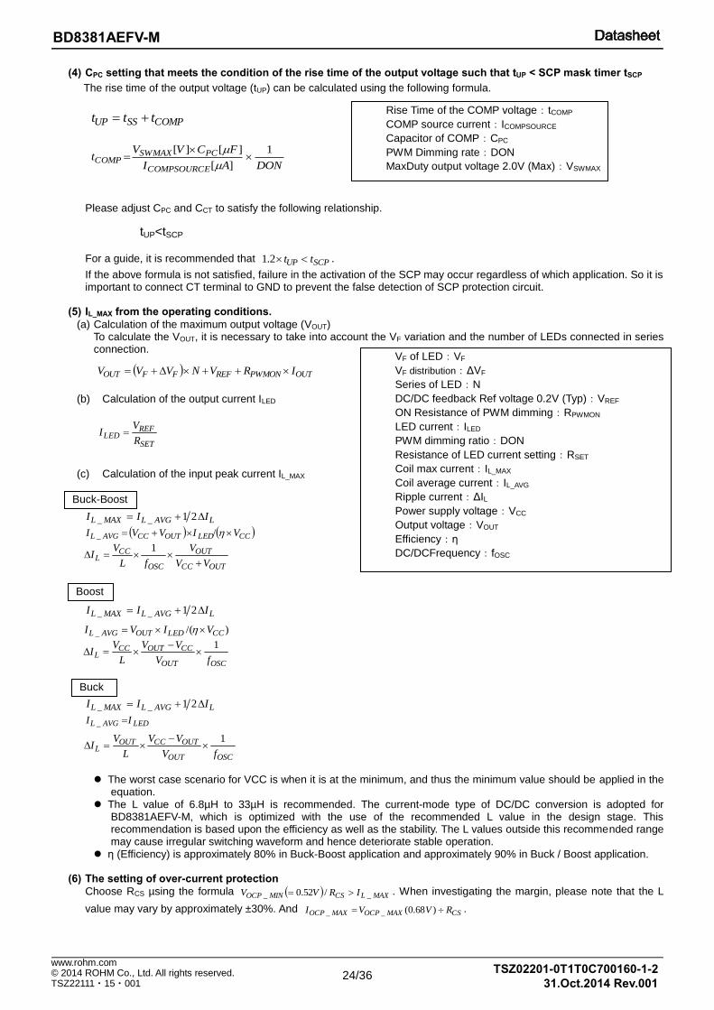
(5) IL_MAX from the operating conditions.
(a) Calculation of the maximum output voltage (VOUT) To calculate the VOUT, it is necessary to take into account the VF variation and the number of LEDs connected in series connection.
(b) Calculation of the output current ILED
(c) Calculation of the input peak current IL_MAX
LAVGLMAXL III 21__
CCLEDOUTCCAVGL VIVVI /_
LAVGLMAXL III 21__
LAVGLMAXL III 21__
LEDAVGL II _
The worst case scenario for VCC is when it is at the minimum, and thus the minimum value should be applied in the equation.
The L value of 6.8µH to 33µH is recommended. The current-mode type of DC/DC conversion is adopted for BD8381AEFV-M, which is optimized with the use of the recommended L value in the design stage. This recommendation is based upon the efficiency as well as the stability. The L values outside this recommended range may cause irregular switching waveform and hence deteriorate stable operation.
η (Efficiency) is approximately 80% in Buck-Boost application and approximately 90% in Buck / Boost application.
(6) The setting of over-current protection Choose RCS µsing the formula MAXLCSMINOCP IRVV __ /52.0 . When investigating the margin, please note that the L
value may vary by approximately ±30%. And CSMAXOCPMAXOCP RVVI )68.0(__ .
(7) The selection of the L In order to achieve stable operation of the current-mode DC/DC converter, we recommend selecting the L value in the ranges indicated below:
sVL
RVsV CSOUT /3.0]/[05.0
sVL
RVVsV CSCCOUT /3.0
)(]/[05.0
Stability will be greatly increased by reducing the calculated value but there is also a possibility that the response will be lowered.
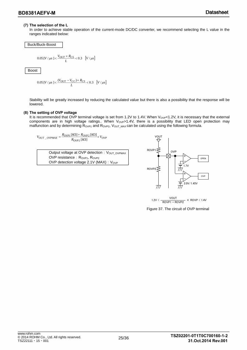
(8) The setting of OVP voltage
It is recommended that OVP terminal voltage is set from 1.2V to 1.4V. When VOVP<1.2V, it is necessary that the external components are in high voltage ratings.. When VOVP>1.4V, there is a possibility that LED open protection may malfunction and by determining ROVP1 and ROVP2, VOUT_MAX can be calculated using the following formula.
Note: In consideration of the external component variations, please design with sufficient margin.
Note: VCC_MAX is the maximum supply voltage, VOUT_MAX is the maximum output voltage detect by OVP.
(10) Selection of the output capacitor
Select the output capacitor COUT based on the requirement of the ripple voltage Vpp.
ESRIMAXLOSCCCOUT
CC
OUT
LED RIfVV
V
C
IVpp
L
)(
12/_
)(11
_ ESRMAXLOSC
LED
OUT
RIf
I
CVpp
OSCOUT
LESRL
fC
IRIVpp
11
8
(11) Selection of the input capacitor A capacitor at the input is also required as the peak current flows between the input and the output terminals in DC/DC conversion. We recommend an input capacitor greater than 10µF with the ESR smaller than 100mΩ. The input capacitor outside of our recommendation may cause large ripple voltage at the input and hence may lead to malfunction.
In general, the negative feedback loop is stable when the following condition is met:
(a) Overall gain of 1 (0dB) with a phase lag of less than 150º (i.e., Phase margin of 30º or more) However, as the DC/DC converter constantly samples the switching frequency, the gain-bandwidth (GBW) product of the entire series should be set to 1/10 of the switching frequency of the system. Therefore, the overall stability characteristics of the application are as follows:
(b) Overall gain of 1 (0dB) with a phase lag of less than 150º (i.e., Phase margin of 30º or more) (c) GBW (frequency at gain 0dB) of 1/10 of the switching frequency
Thus, to improve response within the GBW product limits, the switching frequency must be increased.
The key for achieving stability is to place fz near to the GBW. GBW is decided by phase delay fp1 in terms of COUT and output impedance RL. fz and fp1 are defined by the following formula.
][2
11
2
1
HzRLC
fplagPhase
HzCpcRpc
fzleadPhase
OUT
][OUT
OUTL
I
VR
Good stability would be obtained when the fz is set between 1kHz to 10kHz. Please substitute the value of the maximum load for RL.
In Buck-Boost/ Buck application, Right-Hand-Plane (RHP) Zero exists. This Zero has no gain but a pole characteristic in terms of phase. As this Zero would cause instability when it is in the control loop, it is necessary to bring this zero before the GBW.
where: IOUT: Maximum Load Current
It is important to keep in mind that these are very loose guidelines, and adjustments may have to be made to ensure stability in the actual circuit. It is also important to note that stability characteristics can change greatly depending on factors such as substrate layout and load conditions. Therefore, when designing for mass-production, stability should be thoroughly investigated and confirmed in the actual physical design.
(13) Verification of the operation by taking measurements The overall characteristic may change by load current, input voltage, output voltage, inductance, load capacitance, switching frequency and the PCB layout. We strongly recommend verifying your design by taking the actual measurements.
Connecting the power supply in reverse polarity can damage the IC. Take precautions against reverse polarity when connecting the power supply, such as mounting an external diode between the power supply and the IC’s power supply pins.
2. Power Supply Lines
Design the PCB layout pattern to provide low impedance supply lines. Separate the ground and supply lines of the digital and analog blocks to prevent noise in the ground and supply lines of the digital block from affecting the analog block. Furthermore, connect a capacitor to ground at all power supply pins. Consider the effect of temperature and aging on the capacitance value when using electrolytic capacitors.
3. Ground Voltage
Ensure that no pins are at a voltage below that of the ground pin at any time, even during transient condition.
4. Ground Wiring Pattern When using both small-signal and large-current ground traces, the two ground traces should be routed separately but connected to a single ground at the reference point of the application board to avoid fluctuations in the small-signal ground caused by large currents. Also ensure that the ground traces of external components do not cause variations on the ground voltage. The ground lines must be as short and thick as possible to reduce line impedance.
5. Thermal Consideration
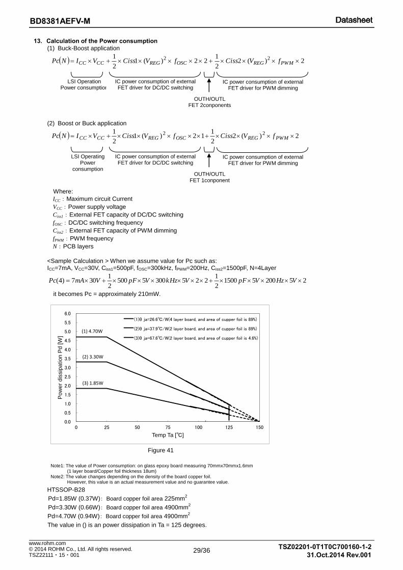
Should by any chance the power dissipation rating be exceeded the rise in temperature of the chip may result in deterioration of the properties of the chip. In case of exceeding this absolute maximum rating, increase the board size and copper area to prevent exceeding the Pd rating.
6. Recommended Operating Conditions
These conditions represent a range within which the expected characteristics of the IC can be approximately obtained. The electrical characteristics are guaranteed under the conditions of each parameter.
7. Inrush Current
When power is first supplied to the IC, it is possible that the internal logic may be unstable and inrush current may flow instantaneously due to the internal powering sequence and delays, especially if the IC has more than one power supply. Therefore, give special consideration to power coupling capacitance, power wiring, width of ground wiring, and routing of connections.
8. Operation Under Strong Electromagnetic Field
Operating the IC in the presence of a strong electromagnetic field may cause the IC to malfunction.
9. Testing on Application Boards
When testing the IC on an application board, connecting a capacitor directly to a low-impedance output pin may subject the IC to stress. Always discharge capacitors completely after each process or step. The IC’s power supply should always be turned off completely before connecting or removing it from the test setup during the inspection process. To prevent damage from static discharge, ground the IC during assembly and use similar precautions during transport and storage.
10. Inter-pin Short and Mounting Errors Ensure that the direction and position are correct when mounting the IC on the PCB. Incorrect mounting may result in damaging the IC. Avoid nearby pins being shorted to each other especially to ground, power supply and output pin. Inter-pin shorts could be due to many reasons such as metal particles, water droplets (in very humid environment) and unintentional solder bridge deposited in between pins during assembly to name a few.
Input pins of an IC are often connected to the gate of a MOS transistor. The gate has extremely high impedance and extremely low capacitance. If left unconnected, the electric field from the outside can easily charge it. The small charge acquired in this way is enough to produce a significant effect on the conduction through the transistor and cause unexpected operation of the IC. So unless otherwise specified, unused input pins should be connected to the power supply or ground line.
12. Regarding the Input Pin of the IC
This monolithic IC contains P+ isolation and P substrate layers between adjacent elements in order to keep them isolated. P-N junctions are formed at the intersection of the P layers with the N layers of other elements, creating a parasitic diode or transistor. For example (refer to figure below):
When GND > Pin A and GND > Pin B, the P-N junction operates as a parasitic diode. When GND > Pin B, the P-N junction operates as a parasitic transistor.
Parasitic diodes inevitably occur in the structure of the IC. The operation of parasitic diodes can result in mutual interference among circuits, operational faults, or physical damage. Therefore, conditions that cause these diodes to operate, such as applying a voltage lower than the GND voltage to an input pin (and thus to the P substrate) should be avoided.
Figure 42. Example of monolithic IC structure
13. Area of Safe Operation (ASO) Operate the IC such that the output voltage, output current, and power dissipation are all within the Area of Safe Operation (ASO).
14. Thermal Shutdown Circuit(TSD)
This IC has a built-in thermal shutdown circuit that prevents heat damage to the IC. Normal operation should always be within the IC’s power dissipation rating. If however the rating is exceeded for a continued period, the junction temperature (Tj) will rise which will activate the TSD circuit that will turn OFF all output pins. When the Tj falls below the TSD threshold, the circuits are automatically restored to normal operation. Note that the TSD circuit operates in a situation that exceeds the absolute maximum ratings and therefore, under no circumstances, should the TSD circuit be used in a set design or for any purpose other than protecting the IC from heat damage.
TSD ON temperature [°C] (typ) Hysteresis temperature [°C] (typ)
1. If you intend to use our Products in devices requiring extremely high reliability (such as medical equipment (Note 1)
, aircraft/spacecraft, nuclear power controllers, etc.) and whose malfunction or failure may cause loss of human life, bodily injury or serious damage to property (“Specific Applications”), please consult with the ROHM sales representative in advance. Unless otherwise agreed in writing by ROHM in advance, ROHM shall not be in any way responsible or liable for any damages, expenses or losses incurred by you or third parties arising from the use of any ROHM’s Products for Specific Applications.
(Note1) Medical Equipment Classification of the Specific Applications
JAPAN USA EU CHINA
CLASSⅢ CLASSⅢ
CLASSⅡb CLASSⅢ
CLASSⅣ CLASSⅢ
2. ROHM designs and manufactures its Products subject to strict quality control system. However, semiconductor
products can fail or malfunction at a certain rate. Please be sure to implement, at your own responsibilities, adequate safety measures including but not limited to fail-safe design against the physical injury, damage to any property, which a failure or malfunction of our Products may cause. The following are examples of safety measures:
[a] Installation of protection circuits or other protective devices to improve system safety [b] Installation of redundant circuits to reduce the impact of single or multiple circuit failure
3. Our Products are not designed under any special or extraordinary environments or conditions, as exemplified below. Accordingly, ROHM shall not be in any way responsible or liable for any damages, expenses or losses arising from the use of any ROHM’s Products under any special or extraordinary environments or conditions. If you intend to use our Products under any special or extraordinary environments or conditions (as exemplified below), your independent verification and confirmation of product performance, reliability, etc, prior to use, must be necessary:
[a] Use of our Products in any types of liquid, including water, oils, chemicals, and organic solvents [b] Use of our Products outdoors or in places where the Products are exposed to direct sunlight or dust [c] Use of our Products in places where the Products are exposed to sea wind or corrosive gases, including Cl2,
H2S, NH3, SO2, and NO2
[d] Use of our Products in places where the Products are exposed to static electricity or electromagnetic waves [e] Use of our Products in proximity to heat-producing components, plastic cords, or other flammable items [f] Sealing or coating our Products with resin or other coating materials [g] Use of our Products without cleaning residue of flux (even if you use no-clean type fluxes, cleaning residue of
flux is recommended); or Washing our Products by using water or water-soluble cleaning agents for cleaning residue after soldering
[h] Use of the Products in places subject to dew condensation
4. The Products are not subject to radiation-proof design. 5. Please verify and confirm characteristics of the final or mounted products in using the Products. 6. In particular, if a transient load (a large amount of load applied in a short period of time, such as pulse. is applied,
confirmation of performance characteristics after on-board mounting is strongly recommended. Avoid applying power exceeding normal rated power; exceeding the power rating under steady-state loading condition may negatively affect product performance and reliability.
7. De-rate Power Dissipation (Pd) depending on Ambient temperature (Ta). When used in sealed area, confirm the actual
ambient temperature. 8. Confirm that operation temperature is within the specified range described in the product specification. 9. ROHM shall not be in any way responsible or liable for failure induced under deviant condition from what is defined in
this document.
Precaution for Mounting / Circuit board design 1. When a highly active halogenous (chlorine, bromine, etc.) flux is used, the residue of flux may negatively affect product
performance and reliability. 2. In principle, the reflow soldering method must be used on a surface-mount products, the flow soldering method must
be used on a through hole mount products. If the flow soldering method is preferred on a surface-mount products, please consult with the ROHM representative in advance.
For details, please refer to ROHM Mounting specification
Precautions Regarding Application Examples and External Circuits 1. If change is made to the constant of an external circuit, please allow a sufficient margin considering variations of the
characteristics of the Products and external components, including transient characteristics, as well as static characteristics.
2. You agree that application notes, reference designs, and associated data and information contained in this document
are presented only as guidance for Products use. Therefore, in case you use such information, you are solely responsible for it and you must exercise your own independent verification and judgment in the use of such information contained in this document. ROHM shall not be in any way responsible or liable for any damages, expenses or losses incurred by you or third parties arising from the use of such information.
Precaution for Electrostatic This Product is electrostatic sensitive product, which may be damaged due to electrostatic discharge. Please take proper caution in your manufacturing process and storage so that voltage exceeding the Products maximum rating will not be applied to Products. Please take special care under dry condition (e.g. Grounding of human body / equipment / solder iron, isolation from charged objects, setting of Ionizer, friction prevention and temperature / humidity control).
Precaution for Storage / Transportation 1. Product performance and soldered connections may deteriorate if the Products are stored in the places where:
[a] the Products are exposed to sea winds or corrosive gases, including Cl2, H2S, NH3, SO2, and NO2 [b] the temperature or humidity exceeds those recommended by ROHM [c] the Products are exposed to direct sunshine or condensation [d] the Products are exposed to high Electrostatic
2. Even under ROHM recommended storage condition, solderability of products out of recommended storage time period may be degraded. It is strongly recommended to confirm solderability before using Products of which storage time is exceeding the recommended storage time period.
3. Store / transport cartons in the correct direction, which is indicated on a carton with a symbol. Otherwise bent leads
may occur due to excessive stress applied when dropping of a carton. 4. Use Products within the specified time after opening a humidity barrier bag. Baking is required before using Products of
which storage time is exceeding the recommended storage time period.
Precaution for Product Label QR code printed on ROHM Products label is for ROHM’s internal use only.
Precaution for Disposition When disposing Products please dispose them properly using an authorized industry waste company.
Precaution for Foreign Exchange and Foreign Trade act Since our Products might fall under controlled goods prescribed by the applicable foreign exchange and foreign trade act, please consult with ROHM representative in case of export.
Precaution Regarding Intellectual Property Rights 1. All information and data including but not limited to application example contained in this document is for reference
only. ROHM does not warrant that foregoing information or data will not infringe any intellectual property rights or any other rights of any third party regarding such information or data. ROHM shall not be in any way responsible or liable for infringement of any intellectual property rights or other damages arising from use of such information or data.:
2. No license, expressly or implied, is granted hereby under any intellectual property rights or other rights of ROHM or any
third parties with respect to the information contained in this document.
Other Precaution 1. This document may not be reprinted or reproduced, in whole or in part, without prior written consent of ROHM. 2. The Products may not be disassembled, converted, modified, reproduced or otherwise changed without prior written
consent of ROHM. 3. In no event shall you use in any way whatsoever the Products and the related technical information contained in the
Products or this document for any military purposes, including but not limited to, the development of mass-destruction weapons.
4. The proper names of companies or products described in this document are trademarks or registered trademarks of
General Precaution 1. Before you use our Pro ducts, you are requested to care fully read this document and fully understand its contents.
ROHM shall n ot be in an y way responsible or liabl e for fa ilure, malfunction or acci dent arising from the use of a ny ROHM’s Products against warning, caution or note contained in this document.
2. All information contained in this docume nt is current as of the issuing date and subj ect to change without any prior
notice. Before purchasing or using ROHM’s Products, please confirm the la test information with a ROHM sale s representative.
3. The information contained in this doc ument is provi ded on an “as is” basis and ROHM does not warrant that all
information contained in this document is accurate an d/or error-free. ROHM shall not be in an y way responsible or liable for any damages, expenses or losses incurred by you or third parties resulting from inaccuracy or errors of or concerning such information.