9
Beatrice Beyer

Beatrice Beyer

[email protected] │ 2017-03-28 2
Organic semiconductors have a lowmobility
Charge carriers need to be pushed through Anode and cathode need to be kept
seperated (otherwise short circuit)
Photolithography• Pro: very accurate, easily be scalable• Contra: flexibility limited by masks, wet
processes are necessary (photo resist andstripper)
Alternatives need to be:• Inexpensive, fast, reproducible and reliable
light emissionthrough graphene
Figure 1. Working principle of organic light emitiing diodes using graphene as electrode.

[email protected] │ 2017-03-28 3
Locally very high temperature formation of 2-3 µm thick folds• Induces short circuits resulting in
„sudden death“ By varying the laser fluence, length and
number of these folds varies
Applied on foils, sacrificial layers areneeded to protect the barrier layer Figure 2. (Top, right) SEM pictures of graphene
edges on glass after laser ablation in dependence on the radiant fluence, (bottom, right) as well as correspoding thermographicimages of resulting OLED devices. (Left) 2D Raman map of seperated graphene layers bylaser ablation.
[email protected] │ 2017-03-28 4
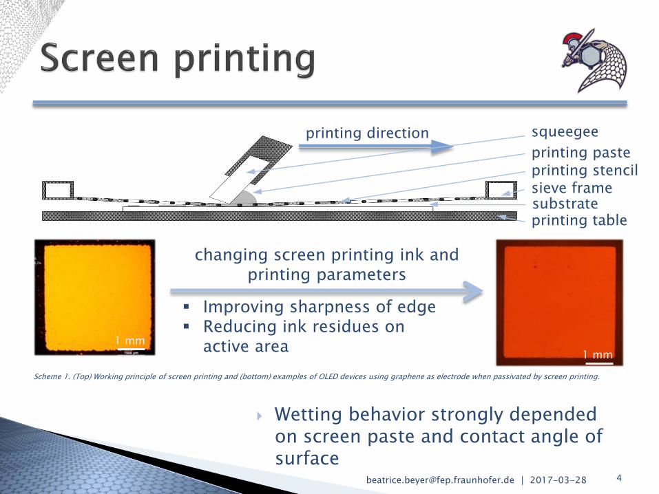
Wetting behavior strongly dependedon screen paste and contact angle ofsurface
1 mm1 mm
changing screen printing ink andprinting parameters
Improving sharpness of edge Reducing ink residues on
active area
printing pasteprinting direction squeegee
printing stencilsieve framesubstrateprinting table
Scheme 1. (Top) Working principle of screen printing and (bottom) examples of OLED devices using graphene as electrode when passivated by screen printing.

[email protected] │ 2017-03-28 5
CVD graphene transferred by chemical etching Deposition of 20 nm of a hole transport layer (HTL) Application of Ar/O2 (1:1) plasma for 120 s thickness
reduction of HTL by 9.1 ± 0.1 nm Subsequent deposition of HTL, blocking and emission layer
followed by hole blocking and electron transport layer
Scheme 2. Schematic presentation of thedevice fabrication: the bare anode (heregraphene) is provided on an insulatingsubstrate, where a hole transport layer(i) with a specified shape is deposited on the anode. (ii) Afterwards an Ar/O2plasma is shortly applied to both theorganic layer and graphene electrodeand stops after the graphene is entirelyetched away, followed by the depositionof a hole transport layer (iii) and otherfunctional layer necessary to completethe OLED (iv). By subsequent depositionof the cathode, the emitting area of theOLED is defined.

[email protected] │ 2017-03-28 6
Plasma etching showsno impact on OLED lifetime• Two different types of HTL
layers have been tested• Variation of different
plasma exposure times
Repetition for grapheneelectrodes
Figure 3. (a) Luminance-current density-voltage (LJV) curves of ITO referencesamples containing a hole transport layer which has not experienced anyplasma etching (light red) and which has (light blue) as well as thecorresponding luminance decay curves determined at three different currents.
[email protected] │ 2017-03-28 7
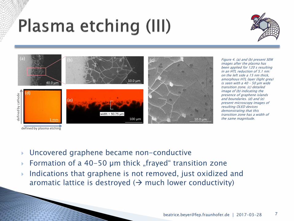
Uncovered graphene became non-conductive Formation of a 40-50 µm thick „frayed“ transition zone Indications that graphene is not removed, just oxidized and
aromatic lattice is destroyed ( much lower conductivity)
Figure 4. (a) and (b) present SEM images after the plasma hasbeen applied for 120 s resultingin an HTL reduction of 5.1 nm: on the left side a 15 nm thick, amorphous HTL layer (light grey) is seen with a 40 – 50 µm widetransition zone. (c) detailedimage of (b) indicating thepresence of graphene islandsand boundaries. (d) and (e) present microscopy images ofresulting OLED devicesdemonstrating that thistransition zone has a width ofthe same magnitude.

[email protected] │ 2017-03-28 8
Plasma etching is a useful method todefine the graphene anode
In particular feasible on polymer foils(does not harm the barrier layers)
Independent on surface energy ofgraphene (i.e. wetting behavior of screenprinting inks)
Works for OLED devices from small (6.4 mm2) to large (3 cm2) areas
3 cm2 OLED 100 cd/m2
electrode v [V]
CD [mA/cm2]
CE [cd/A]
LE [lm/W]
EQE [%]
J(-5 V) [mA/cm2]
graphenea) 6.1 1.9) 5.3 2.7 4.1 1.1×10⁻⁴
ITOb) 2.7 0.8 13.3 15.9 10.3 2.5×10⁻⁵
a) has been structured by plasma etching; b) has been structured by laser ablation.
Table 1. Overview of 3 cm2 OLED performance for both grapheneand ITO .
Figure 5. Example of a flexible, transparent OLED with an emitting area of 1.5×2 (cm)2 after patterning it by plasma etching (a-d) and its JV
characteristic compared to the ITO reference.

[email protected] │ 2017-03-28 9
Fraunhofer FEP: David Wynands, André Philipp, Falk Schütze Graphenea: Amaia Pesquera, Amaia Zurutuza Technical University of Denmark / Nanotech: Patrick Rebsdorf
Whelan, Tim Booth
The research leading to these results has received funding from the European Union Seventh Framework Programme FP7/2007-2013 under grant agreement n° 604000 (GLADIATOR)
Project Officer: Dr. Martyn Chamberlain, EC Project Coordinator: Dr. Beatrice Beyer, Fraunhofer FEP
Website: www.graphene-gladiator.eu Email: [email protected]


