U.P.B. Sci. Bull., Series C, Vol. 74, Iss. 3, 2012 ISSN 1454-234x BEHAVIOR OF ELECTRICAL STRESSED FLEXIBLE RESISITVE LAYER PART I: CARBON FILLED POLYMER Detlef BONFERT 1 , Paul SVASTA 2 , Ciprian IONESCU 3 Includerea senzorilor rezistivi în designul dispozitivelor electronice organice este necesară pentru a extinde domeniul aplicaţiilor posibile. Pentru aceasta este necesară identificarea materialelor rezistive, a proceselor şi metodelor de structurare, precum şi analiza proprietăţilor rezistive pe substrat flexibil ale acestora. Două materiale cu aplicaţie largă în electronica organică sunt polimerii umpluţi cu carbon (carbon filled polymer, CFP) şi polimerii cu conducţie intrinsecă (ICP, poly (3, 4-ethylendioxythiophene) doped with polystyrene sulfonate acid, PEDOT:PSS). Lucrarea are ca scop prezentarea comportării acestor polimeri conductivi pe suport flexibil sub influenţa curentului continuu şi în impulsuri, subliniind variaţiile rezultate ale proprietăţilor rezistive. Lucrarea este prezentată în două părţi, prima parte analizează comportarea polimerilor umpluţi cu carbon iar partea a doua pune accentul pe polimerii cu conducţie intrinsecă. There is a necessity to include sensors (resistors) in the design of organic electronic devices in order to extend the range of possible applications. It is essential to identify potential resistive materials, the processes and methods to structure them and to analyze their resistive properties on flexible substrates. Two materials widely used in organic electronics are carbon filled polymer (CFP) and the intrinsically conductive polymer (ICP) poly (3, 4-ethylendioxythiophene) doped with polystyrene sulfonate acid (PEDOT:PSS). In this paper we focus on the DC and pulsed stress behavior of these conductive polymers on flexible substrates and the resulting changes of their resistive properties. The paper is presented in two parts. Part one deals with carbon filled polymers (CFPs)and part two analyzes the behavior of intrinsically conductive polymesrs (ICPs). Keywords: Thick Film Flexible Resistors, Carbon filled polymer, PEDOT:PSS, DC- and Pulsed Stress 1 Researcher, Polytronics Dept., Fraunhofer EMFT, Munich, Germany, e-mail: [email protected]2 Prof., Electronics Faculty, CETTI, University POLITEHNICA of Bucharest, Romania, e-mail: [email protected]3 Conf., Electronics Faculty, CETTI, University POLITEHNICA of Bucharest, Romania, e-mail: [email protected]
BEHAVIOR OF ELECTRICAL STRESSED FLEXIBLE RESISITVE LAYER
PART I: CARBON FILLED POLYMER
Detlef BONFERT1, Paul SVASTA2, Ciprian IONESCU3
Includerea senzorilor rezistivi în designul dispozitivelor electronice organice este necesară pentru a extinde domeniul aplicaţiilor posibile. Pentru aceasta este necesară identificarea materialelor rezistive, a proceselor şi metodelor de structurare, precum şi analiza proprietăţilor rezistive pe substrat flexibil ale acestora. Două materiale cu aplicaţie largă în electronica organică sunt polimerii umpluţi cu carbon (carbon filled polymer, CFP) şi polimerii cu conducţie intrinsecă (ICP, poly (3, 4-ethylendioxythiophene) doped with polystyrene sulfonate acid, PEDOT:PSS). Lucrarea are ca scop prezentarea comportării acestor polimeri conductivi pe suport flexibil sub influenţa curentului continuu şi în impulsuri, subliniind variaţiile rezultate ale proprietăţilor rezistive. Lucrarea este prezentată în două părţi, prima parte analizează comportarea polimerilor umpluţi cu carbon iar partea a doua pune accentul pe polimerii cu conducţie intrinsecă.
There is a necessity to include sensors (resistors) in the design of organic electronic devices in order to extend the range of possible applications. It is essential to identify potential resistive materials, the processes and methods to structure them and to analyze their resistive properties on flexible substrates. Two materials widely used in organic electronics are carbon filled polymer (CFP) and the intrinsically conductive polymer (ICP) poly (3, 4-ethylendioxythiophene) doped with polystyrene sulfonate acid (PEDOT:PSS). In this paper we focus on the DC and pulsed stress behavior of these conductive polymers on flexible substrates and the resulting changes of their resistive properties. The paper is presented in two parts. Part one deals with carbon filled polymers (CFPs)and part two analyzes the behavior of intrinsically conductive polymesrs (ICPs).
Keywords: Thick Film Flexible Resistors, Carbon filled polymer, PEDOT:PSS, DC- and Pulsed Stress
There is a necessity to include sensors, based on resistive effects, in the design of organic electronic devices in order to extend the range of possible applications, mentioned in the last iNEMI roadmap. It is essential to identify potential organic resistive materials, the processes and methods to structure them and to characterize their resistive properties on flexible substrates including their reliability.
One of the most important issues is their stability under different electrical and non electrical influences such as mechanical, thermal stress together with humidity. Highly isolating flexible substrates make the devices even more susceptible to transient electrical stress events, like Electro Static Discharge (ESD).
Passive components are becoming susceptible to ESD events as their geometries are reducing. Integrating and embedding makes them even more vulnerable. Thick film is one main technology in producing resistive passive components on flexible substrates used in polytronics.
Two materials widely used in organic electronics are carbon filled polymer (CFP) and the intrinsically conductive polymer (ICP) poly (3, 4-ethylendioxythiophene) doped with polystyrene sulfonate acid (PEDOT:PSS).
Dispersing electrically conductive fillers into an isolating plastic matrix above a threshold concentration (percolation threshold) will result after curing in a conducting layer [1], [2], [3] and [4]. Carbon black (CB) is a widely used conductive filler which also improves dimensional and ultraviolet light stability, covering a wide square resistance range from ohms to Megohms.
The scientific importance, the properties and the growing applications of PEDOT:PSS, a polythiophene derivative, are presented in [5], [6] and [7]. This material has unique electrical (high conductivity) [5], [6], optical (high visible- light transmission)[6], [8], thermal [6], [8], and mechanical (high stability) [10], [11] properties. Due to this fact there is a wide application range for this polymer, like antistatic coatings, transparent conductor, conducting layer in capacitors, conducting layers for printed wiring boards, hole injection layer in organic light emitting diodes (OLED), conductor and semiconductor layer in organic thin film transistors (OFET), thermal and mechanical sensors.
The ESD behavior of thick film resistors has been reported in several studies [12]-[15], using RC- pulses, which lead to HBM-like discharges. They all report a resistance change after pulse application. A thermal failure model for thick film printed resistors is developed by D.C. Wunsch [15], similar to that for semiconductor devices. Overheating is considered to be the principle failure mechanism.
Electrical stressed flexible resistive layer 61
An efficient technique for electrostatic discharge (ESD) measurements is to use square pulses. Rectangular pulses from Transmission Line Pulsers (TLP) are of particular interest for ESD measurements. They have been well established for the analysis of ESD- protection structures [16], [17] and [18]. This analytical test technique on the basis of square pulses allows the in- situ monitoring of the voltages and currents at the DUT, during pulsing and helps to gain fundamental insights into the electrical behavior.
In [19] and [20] the authors made an introduction to the TLP- measurement technique on thick film resistors. In [21] the TLP characterization of off- chip polymer ESD protection devices is presented. In this work the analysis is made on the flexible carbon based polymer thick film resistors and on intrinsically conductive polymer PEDOT:PSS layer, during DC- stress, single and multiple pulse stress, showing the behavior before, during and after the stress.
The mentioned conductive polymer layers are realized by screen printing in a roll-to-roll process on foil.
2. Test setup
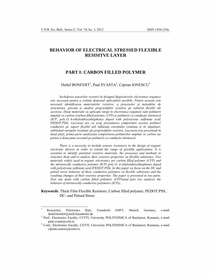
The test setup for pulsing the polymer resistive layers is shown in Fig. 2.1. It consists of the pulse generator, the DC measurement and the test fixture with the DUT.
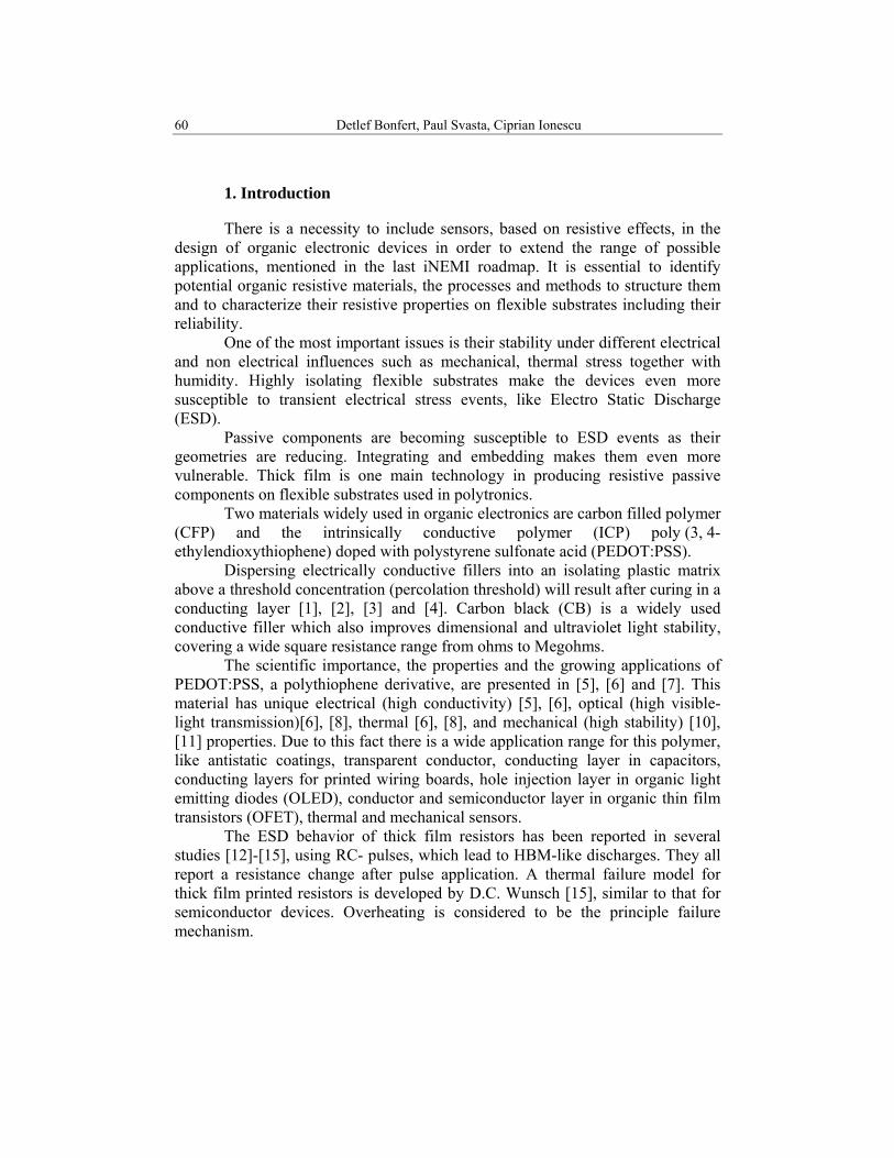
For the characterization of flexible thin film polymer layer the Time Domain Reflection (TDR) configuration of the TLP was used, with 100 ns wide pulses. Fig. 2.2 presents a simplified schematic of the TLP system for this configuration.
V,I
R
Fig. 2.1. Principle of flexible resistive layer stressing and measuring
62 Detlef Bonfert, Paul Svasta, Ciprian Ionescu
HV TL1TL2 TL3
DCSpotMeas.
NINoiseIndex
ZImped.meas.
+-
TLP
I R I IZI dB
V
V V V f f
t t
II V
DUT
DSO I, V
IncidentReflected
Current, voltagetransients
Current- voltagecharacteristic
Stress measurements
DC-, HF-, Noisemeasurements in SOA
Pulsed resistancecharacteristic
Fig. 2.2. Schematic of pulsed stressing and measuring.
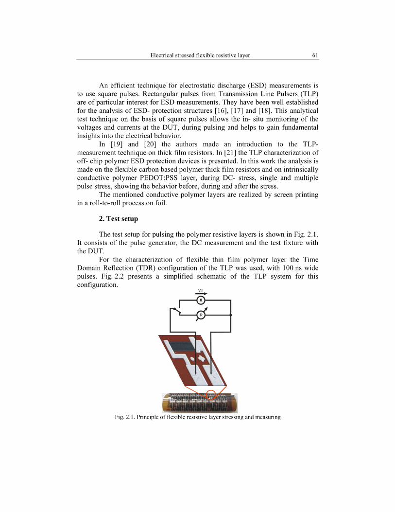
An incident voltage pulse, defined by the length of charging transmission line (TL1), travels from the pulse generator to the device under test (DUT) and may be reflected at the DUT. The voltage of the incident and reflected pulse is measured with a passive voltage probe close to the DUT, so that both pulses can be recorded. The current of the incident and reflected pulse is measured by a current probe.
For 100 ns and wider pulses the measured incident and reflected voltages and currents overlap, if the measurement points are close enough to the DUT (TDR-O configuration if TL3 is of short length). Voltages and currents of the DUT can be directly measured. An example of the pulsed voltage across and the pulsed current into the DUT for a TLP of 100ns pulse width, in the TDR-O configuration, is presented in Fig. 2.3.
Transient Voltage and Current, TLP 100 ns, 100 V, Polymer PEDOT/PSS on PET, R1A
-100
102030405060708090
-20 0 20 40 60 80 100 120 140Time / ns
Pul
sed
Vol
tage
/ V
-0.4-0.20.00.20.40.60.81.01.21.4
Pul
sed
Cur
rent
/ A
TLP-VoltTLP-Curr
Pulsed voltage
Pulsed current
Fig. 2.3. Pulsed voltage across and pulsed current into the DUT for 100 ns TLP (TDR-O).
Electrical stressed flexible resistive layer 63
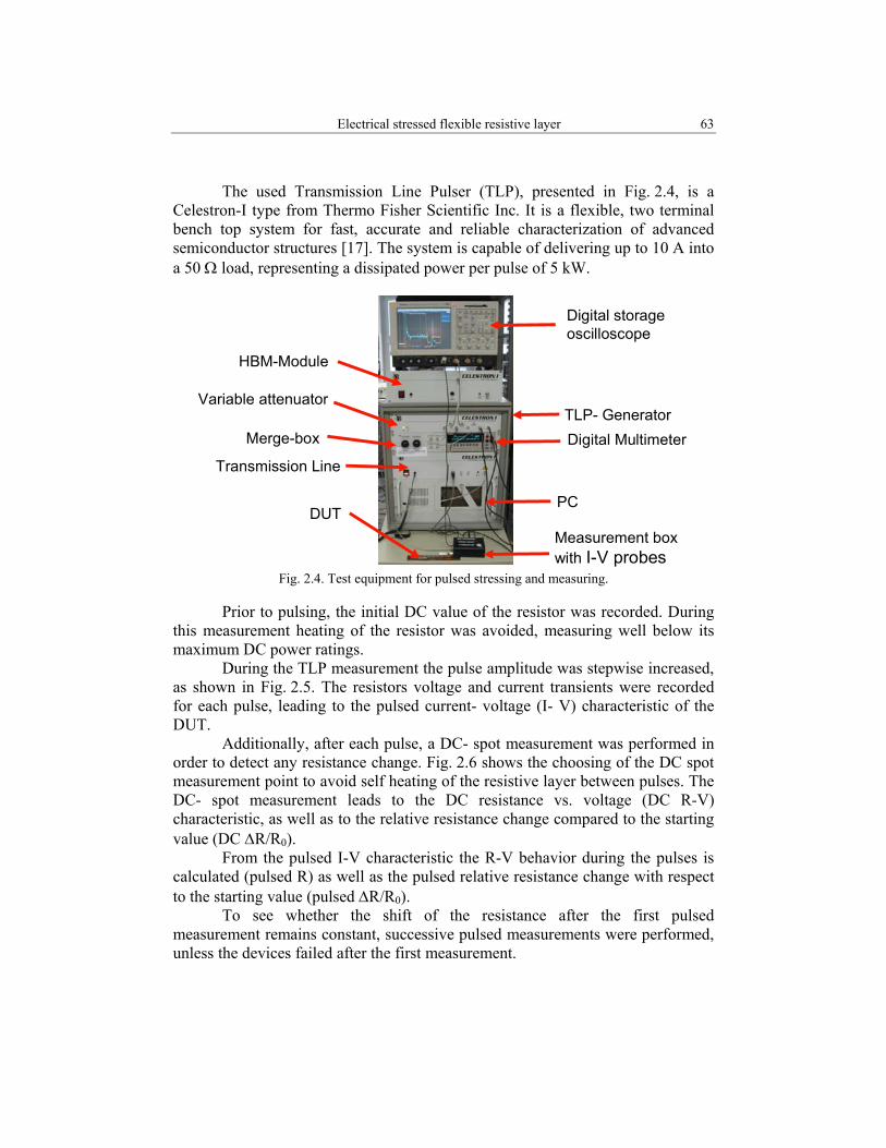
The used Transmission Line Pulser (TLP), presented in Fig. 2.4, is a Celestron-I type from Thermo Fisher Scientific Inc. It is a flexible, two terminal bench top system for fast, accurate and reliable characterization of advanced semiconductor structures [17]. The system is capable of delivering up to 10 A into a 50 Ω load, representing a dissipated power per pulse of 5 kW.
Digital storage oscilloscope
TLP- GeneratorDigital Multimeter
PC
Measurement box with I-V probes
DUT
Transmission Line
Merge-box
Variable attenuator
HBM-Module
Fig. 2.4. Test equipment for pulsed stressing and measuring.
Prior to pulsing, the initial DC value of the resistor was recorded. During
this measurement heating of the resistor was avoided, measuring well below its maximum DC power ratings.
During the TLP measurement the pulse amplitude was stepwise increased, as shown in Fig. 2.5. The resistors voltage and current transients were recorded for each pulse, leading to the pulsed current- voltage (I- V) characteristic of the DUT.
Additionally, after each pulse, a DC- spot measurement was performed in order to detect any resistance change. Fig. 2.6 shows the choosing of the DC spot measurement point to avoid self heating of the resistive layer between pulses. The DC- spot measurement leads to the DC resistance vs. voltage (DC R-V) characteristic, as well as to the relative resistance change compared to the starting value (DC ΔR/R0).
From the pulsed I-V characteristic the R-V behavior during the pulses is calculated (pulsed R) as well as the pulsed relative resistance change with respect to the starting value (pulsed ΔR/R0).
To see whether the shift of the resistance after the first pulsed measurement remains constant, successive pulsed measurements were performed, unless the devices failed after the first measurement.
64 Detlef Bonfert, Paul Svasta, Ciprian Ionescu
Applying high voltage pulses with constant amplitude gives information about the robustness of the DUT to TLP stress.
TimeP1
Pulse
num
ber
Pulse amplitude
P2P3
Pn
P1P2
P3
Pn
Fig. 2.5. Principle of stressing and measurement technique with successive pulsing.
Carbon Resistor ESL 12112, Tempered, Double Current Sweep 0-10mA, R11, PI Foil 12, M2
0
1
2
3
4
5
6
7
8
0 1 2 3 4 5 6 7 8 9 10Current / mA
Volta
ge /
V
690
700
710
720
730
740
R4P
-K /
Ω
VoltageResistance
DC spot- measurement point between pulses, should avoid self heating
Fig. 2.6. Choosing the DC-.spot measurement point, avoiding self heating, for device
characterization between stress pulses. In order to connect the flexible thin film devices to the TLP, a special
DUT test fixture has been developed, using a 50 Ω environment.
3. Carbon based polymer resistive layer
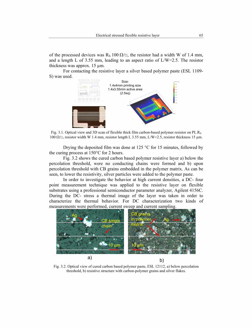
The resistive test structures were realized in thick film technology in a screen printing roll-to-roll process. The printed polymer resistor paste (ESL RS-12112) is designed for the use on polyimide foils and ceramic substrates. Fig. 3.1 gives an optical view and a 3D scan of the tested flexible thick film carbon-based polymer resistor on polyimide (PI) foil, (Upilex S). The nominal sheet resistance
Electrical stressed flexible resistive layer 65
of the processed devices was RS 100 Ω/□, the resistor had a width W of 1.4 mm, and a length L of 3.55 mm, leading to an aspect ratio of L/W=2.5. The resistor thickness was approx. 15 µm.
For contacting the resistive layer a silver based polymer paste (ESL 1109-S) was used.
Size:1.4x4mm printing size
1.4x3.55mm active area(2.5sq)
Fig. 3.1. Optical view and 3D scan of flexible thick film carbon-based polymer resistor on PI, RS
100 Ω/□, resistor width W 1.4 mm, resistor length L 3.55 mm, L/W=2.5, resistor thickness 15 µm. Drying the deposited film was done at 125 °C for 15 minutes, followed by
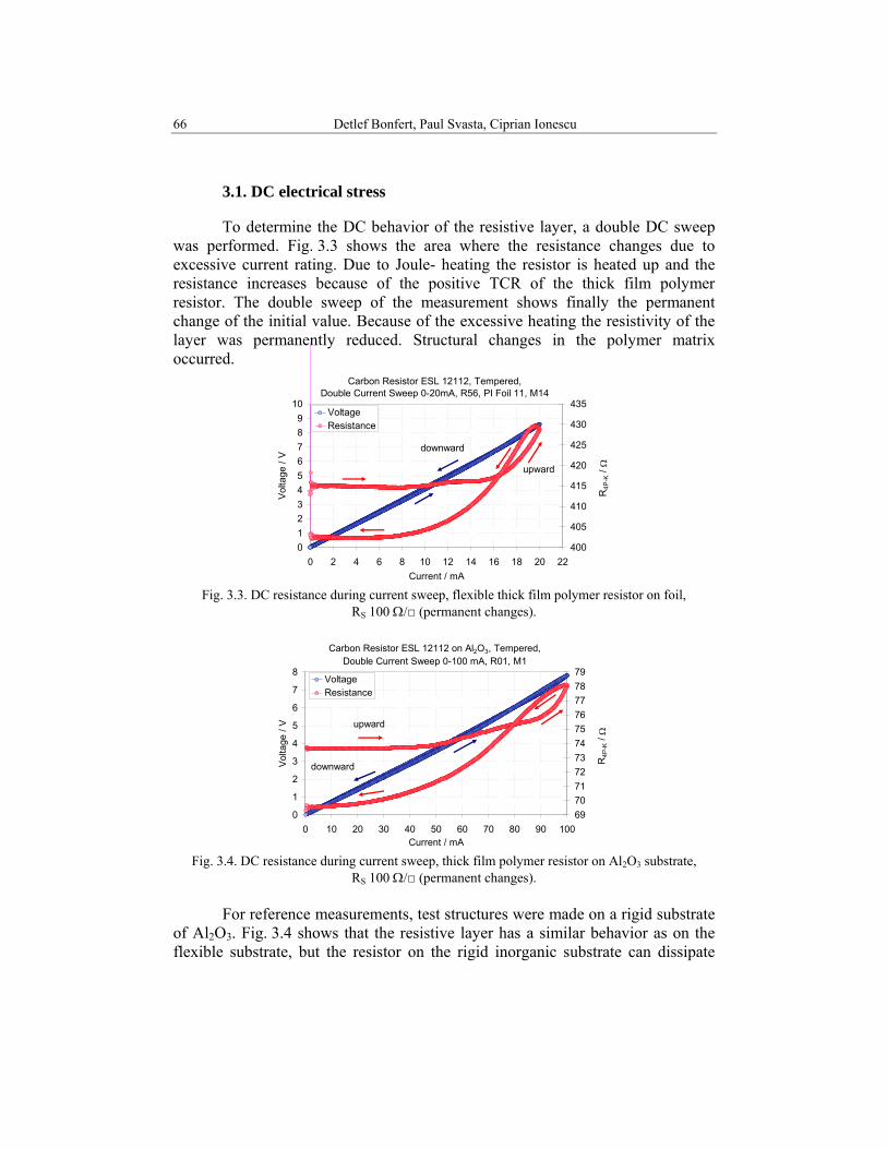
the curing process at 150°C for 2 hours. Fig. 3.2 shows the cured carbon based polymer resistive layer a) below the
percolation threshold, were no conducting chains were formed and b) upon percolation threshold with CB grains embedded in the polymer matrix. As can be seen, to lower the resistivity, silver particles were added to the polymer paste.
In order to investigate the behavior at high current densities, a DC- four point measurement technique was applied to the resistive layer on flexible substrates using a professional semiconductor parameter analyzer, Agilent 4156C. During the DC- stress a thermal image of the layer was taken in order to characterize the thermal behavior. For DC characterization two kinds of measurements were performed, current sweep and current sampling.
10 µm 10 µm
a) b)
AgCB singlechain
AgCB grainsin polymer matrix
Fig. 3.2. Optical view of cured carbon based polymer paste, ESL 12112, a) below percolation
threshold, b) resistive structure with carbon-polymer grains and silver flakes.
66 Detlef Bonfert, Paul Svasta, Ciprian Ionescu
3.1. DC electrical stress
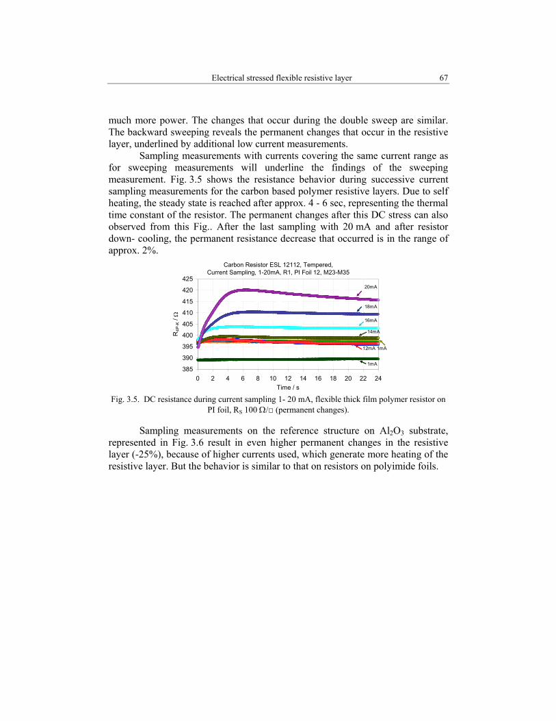
To determine the DC behavior of the resistive layer, a double DC sweep was performed. Fig. 3.3 shows the area where the resistance changes due to excessive current rating. Due to Joule- heating the resistor is heated up and the resistance increases because of the positive TCR of the thick film polymer resistor. The double sweep of the measurement shows finally the permanent change of the initial value. Because of the excessive heating the resistivity of the layer was permanently reduced. Structural changes in the polymer matrix occurred.
Carbon Resistor ESL 12112, Tempered, Double Current Sweep 0-20mA, R56, PI Foil 11, M14
0123456789
10
0 2 4 6 8 10 12 14 16 18 20 22Current / mA
Volta
ge /
V
400
405
410
415
420
425
430
435
R4P
-K /
Ω
VoltageResistance
upward
downward
Fig. 3.3. DC resistance during current sweep, flexible thick film polymer resistor on foil,
RS 100 Ω/□ (permanent changes).
Carbon Resistor ESL 12112 on Al2O3, Tempered, Double Current Sweep 0-100 mA, R01, M1
0
1
2
3
4
5
6
7
8
0 10 20 30 40 50 60 70 80 90 100Current / mA
Vol
tage
/ V
6970717273747576777879
R4P
-K /
Ω
VoltageResistance
upward
downward
Fig. 3.4. DC resistance during current sweep, thick film polymer resistor on Al2O3 substrate,
RS 100 Ω/□ (permanent changes). For reference measurements, test structures were made on a rigid substrate
of Al2O3. Fig. 3.4 shows that the resistive layer has a similar behavior as on the flexible substrate, but the resistor on the rigid inorganic substrate can dissipate
Electrical stressed flexible resistive layer 67
much more power. The changes that occur during the double sweep are similar. The backward sweeping reveals the permanent changes that occur in the resistive layer, underlined by additional low current measurements.
Sampling measurements with currents covering the same current range as for sweeping measurements will underline the findings of the sweeping measurement. Fig. 3.5 shows the resistance behavior during successive current sampling measurements for the carbon based polymer resistive layers. Due to self heating, the steady state is reached after approx. 4 - 6 sec, representing the thermal time constant of the resistor. The permanent changes after this DC stress can also observed from this Fig.. After the last sampling with 20 mA and after resistor down- cooling, the permanent resistance decrease that occurred is in the range of approx. 2%.
Carbon Resistor ESL 12112, Tempered, Current Sampling, 1-20mA, R1, PI Foil 12, M23-M35
385
390
395
400
405
410
415
420
425
0 2 4 6 8 10 12 14 16 18 20 22 24Time / s
R4P
-K /
Ω
18mA
16mA
14mA
1mA12mA
1mA
20mA
Fig. 3.5. DC resistance during current sampling 1- 20 mA, flexible thick film polymer resistor on
PI foil, RS 100 Ω/□ (permanent changes).
Sampling measurements on the reference structure on Al2O3 substrate, represented in Fig. 3.6 result in even higher permanent changes in the resistive layer (-25%), because of higher currents used, which generate more heating of the resistive layer. But the behavior is similar to that on resistors on polyimide foils.
68 Detlef Bonfert, Paul Svasta, Ciprian Ionescu
Carbon Resistor ESL 12112 on Al2O3, Tempered, Current Sampling, 1-100mA, R1, , M4-M12
50.0
55.0
60.0
65.0
70.0
75.0
80.0
85.0
90.0
0 2 4 6 8 10 12 14 16 18 20 22 24Time / s
R4P
-K /
Ω
1mA10mA25mA50mA75mA100mA1mA b100mA b1mA c
1mA, M4 50mA, M7
75mA, M8
100mA, M9
1mA, M10
100mA, M11
1mA, M12
25 %
Fig. 3.6. DC resistance during current sampling 1- 100 mA, thick film polymer resistor on Al2O3
substrate, RS 100 Ω/□ (permanent changes).
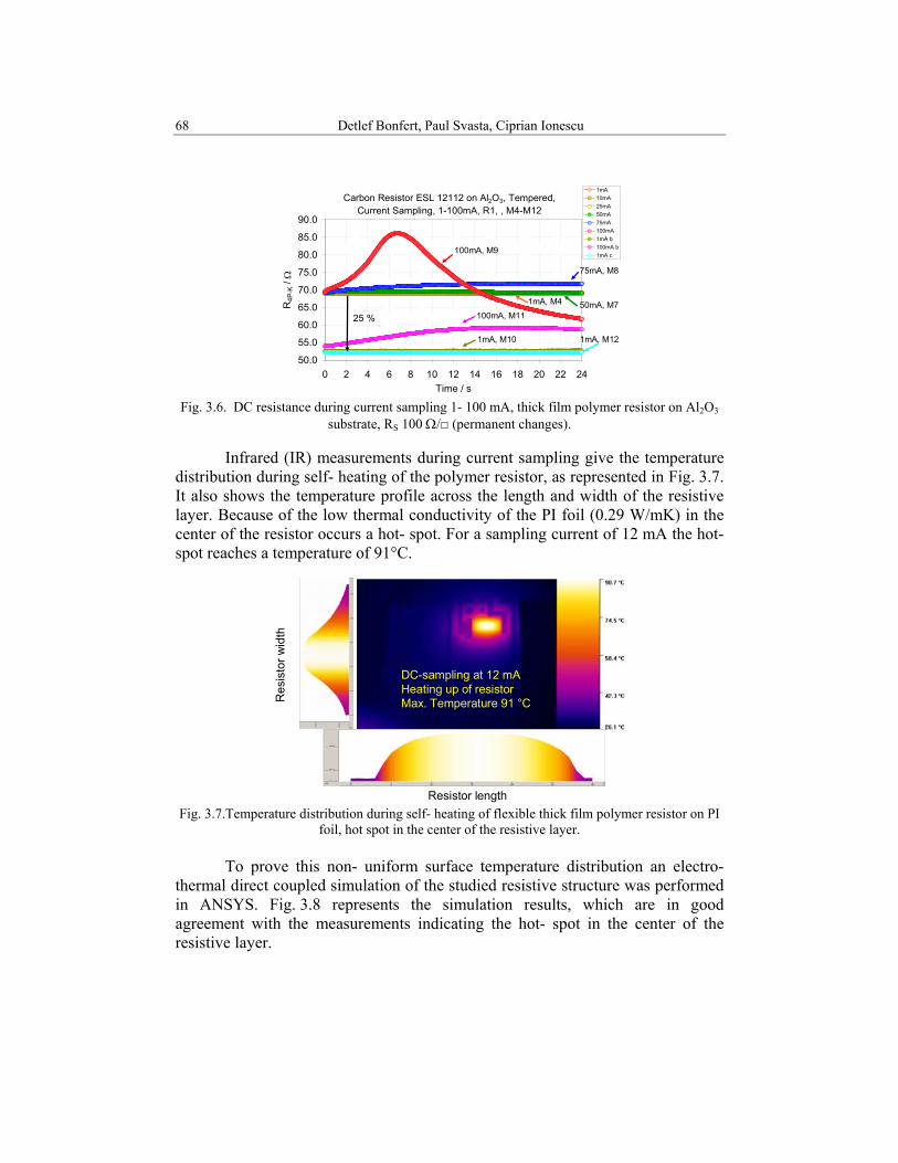
Infrared (IR) measurements during current sampling give the temperature distribution during self- heating of the polymer resistor, as represented in Fig. 3.7. It also shows the temperature profile across the length and width of the resistive layer. Because of the low thermal conductivity of the PI foil (0.29 W/mK) in the center of the resistor occurs a hot- spot. For a sampling current of 12 mA the hot- spot reaches a temperature of 91°C.
Res
isto
r wid
th
Resistor length
DC-sampling at 12 mAHeating up of resistorMax. Temperature 91 °C
Fig. 3.7.Temperature distribution during self- heating of flexible thick film polymer resistor on PI
foil, hot spot in the center of the resistive layer. To prove this non- uniform surface temperature distribution an electro-
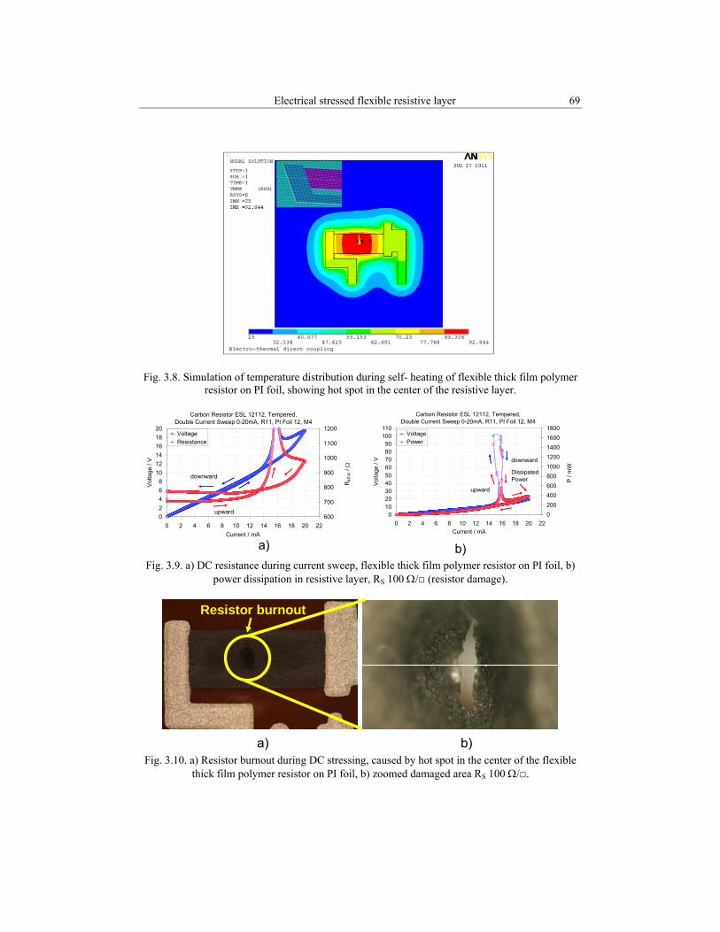
thermal direct coupled simulation of the studied resistive structure was performed in ANSYS. Fig. 3.8 represents the simulation results, which are in good agreement with the measurements indicating the hot- spot in the center of the resistive layer.
Electrical stressed flexible resistive layer 69
Fig. 3.8. Simulation of temperature distribution during self- heating of flexible thick film polymer
resistor on PI foil, showing hot spot in the center of the resistive layer.
a) b)
Carbon Resistor ESL 12112, Tempered, Double Current Sweep 0-20mA, R11, PI Foil 12, M4
0102030405060708090
100110
0 2 4 6 8 10 12 14 16 18 20 22Current / mA
Volta
ge /
V
020040060080010001200140016001800
P / m
W
VoltagePower
upward
downward
DissipatedPower
Carbon Resistor ESL 12112, Tempered, Double Current Sweep 0-20mA, R11, PI Foil 12, M4
02468
101214161820
0 2 4 6 8 10 12 14 16 18 20 22Current / mA
Volta
ge /
V
600
700
800
900
1000
1100
1200
R4P
-K /
Ω
VoltageResistance
upward
downward
Fig. 3.9. a) DC resistance during current sweep, flexible thick film polymer resistor on PI foil, b)
power dissipation in resistive layer, RS 100 Ω/□ (resistor damage).
a) b)
Resistor burnout
Fig. 3.10. a) Resistor burnout during DC stressing, caused by hot spot in the center of the flexible
thick film polymer resistor on PI foil, b) zoomed damaged area RS 100 Ω/□.
70 Detlef Bonfert, Paul Svasta, Ciprian Ionescu
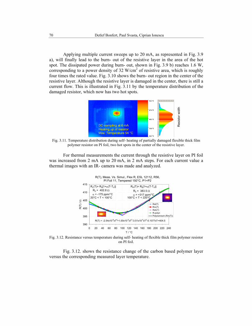
Applying multiple current sweeps up to 20 mA, as represented in Fig. 3.9 a), will finally lead to the burn- out of the resistive layer in the area of the hot spot. The dissipated power during burn- out, shown in Fig. 3.9 b) reaches 1.6 W, corresponding to a power density of 32 W/cm2 of resistive area, which is roughly four times the rated value. Fig. 3.10 shows the burn- out region in the center of the resistive layer. Although the resistive layer is damaged in the center, there is still a current flow. This is illustrated in Fig. 3.11 by the temperature distribution of the damaged resistor, which now has two hot spots.
Res
isto
r wid
th
DC-sampling at 6 mAHeating up of resistorMax. Temperature 54 °C
Fig. 3.11. Temperature distribution during self- heating of partially damaged flexible thick film
polymer resistor on PI foil, two hot spots in the center of the resistive layer. For thermal measurements the current through the resistive layer on PI foil
was increased from 2 mA up to 20 mA, in 2 mA steps. For each current value a thermal images with an IR- camera was made and analyzed.
Fig. 3.12. Resistance versus temperature during self- heating of flexible thick film polymer resistor
on PI foil.
Fig. 3.12. shows the resistance change of the carbon based polymer layer versus the corresponding measured layer temperature.
Electrical stressed flexible resistive layer 71
3.2 Pulsed electrical stress
The behavior of the carbon based resistive layer during pulsed stress was studied applying 100 ns wide pulses from transmission line pulser with increasing and constant amplitudes.
3.2.1 Influence of pulse amplitude on resistance
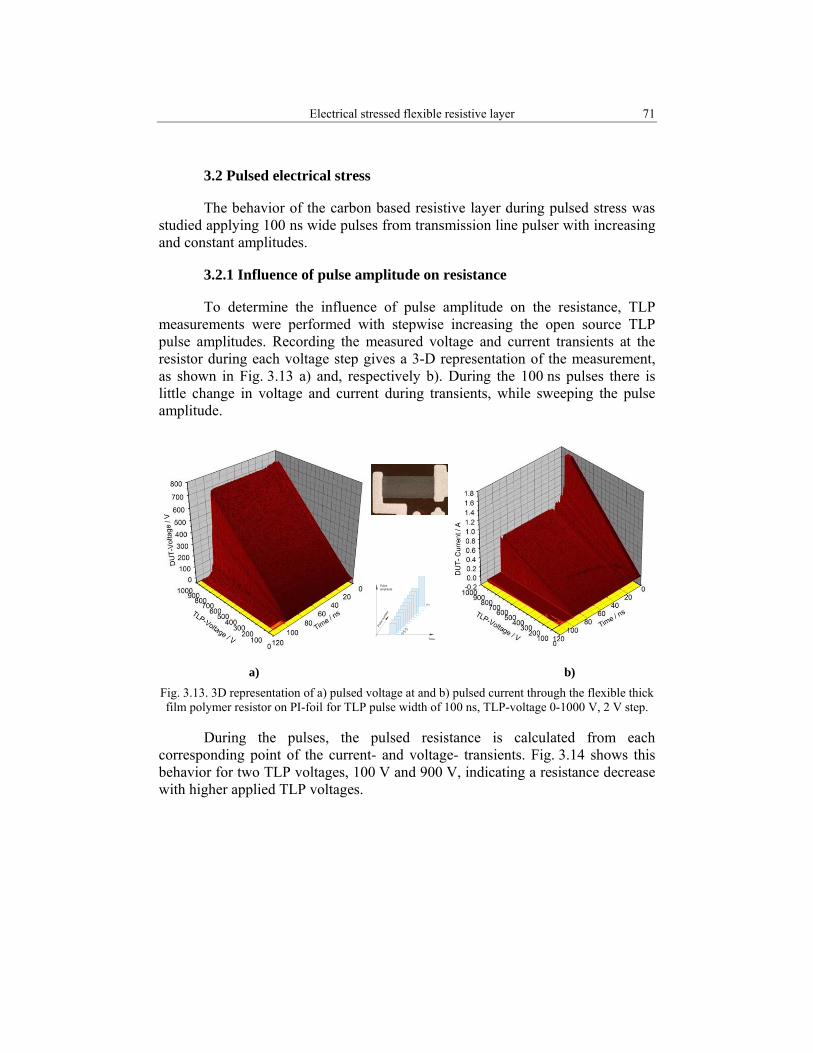
To determine the influence of pulse amplitude on the resistance, TLP measurements were performed with stepwise increasing the open source TLP pulse amplitudes. Recording the measured voltage and current transients at the resistor during each voltage step gives a 3-D representation of the measurement, as shown in Fig. 3.13 a) and, respectively b). During the 100 ns pulses there is little change in voltage and current during transients, while sweeping the pulse amplitude.
Time
P1
Pulse
num
ber
Pulse amplitude
P2P3
Pn
a) b) Fig. 3.13. 3D representation of a) pulsed voltage at and b) pulsed current through the flexible thick film polymer resistor on PI-foil for TLP pulse width of 100 ns, TLP-voltage 0-1000 V, 2 V step.
During the pulses, the pulsed resistance is calculated from each
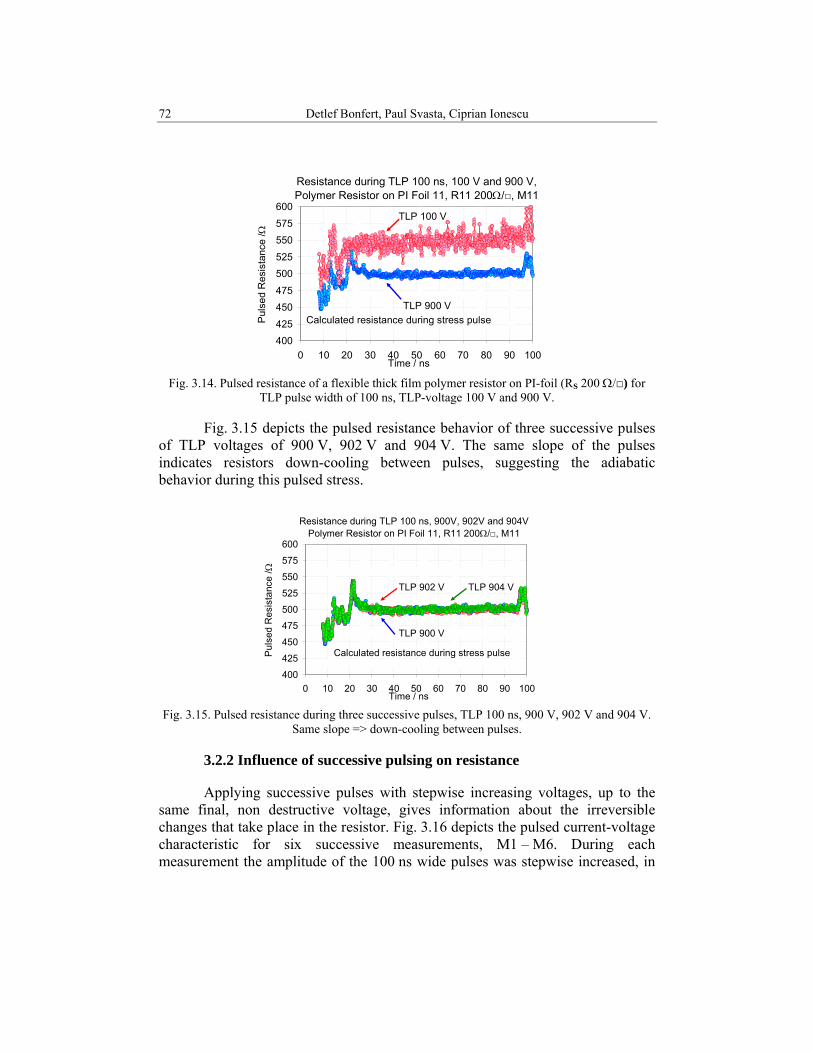
corresponding point of the current- and voltage- transients. Fig. 3.14 shows this behavior for two TLP voltages, 100 V and 900 V, indicating a resistance decrease with higher applied TLP voltages.
72 Detlef Bonfert, Paul Svasta, Ciprian Ionescu
Resistance during TLP 100 ns, 100 V and 900 V, Polymer Resistor on PI Foil 11, R11 200Ω/□, M11
400425
450475
500525
550575
600
0 10 20 30 40 50 60 70 80 90 100Time / ns
Pul
sed
Res
ista
nce
/ Ω
Calculated resistance during stress pulseTLP 900 V
TLP 100 V
Fig. 3.14. Pulsed resistance of a flexible thick film polymer resistor on PI-foil (RS 200 Ω/□) for
TLP pulse width of 100 ns, TLP-voltage 100 V and 900 V.
Fig. 3.15 depicts the pulsed resistance behavior of three successive pulses of TLP voltages of 900 V, 902 V and 904 V. The same slope of the pulses indicates resistors down-cooling between pulses, suggesting the adiabatic behavior during this pulsed stress.
Resistance during TLP 100 ns, 900V, 902V and 904V Polymer Resistor on PI Foil 11, R11 200Ω/□, M11
400
425
450
475
500
525
550
575
600
0 10 20 30 40 50 60 70 80 90 100Time / ns
Pul
sed
Res
ista
nce
/ Ω
Calculated resistance during stress pulse
TLP 900 V
TLP 902 V TLP 904 V
Fig. 3.15. Pulsed resistance during three successive pulses, TLP 100 ns, 900 V, 902 V and 904 V.
Same slope => down-cooling between pulses.
3.2.2 Influence of successive pulsing on resistance
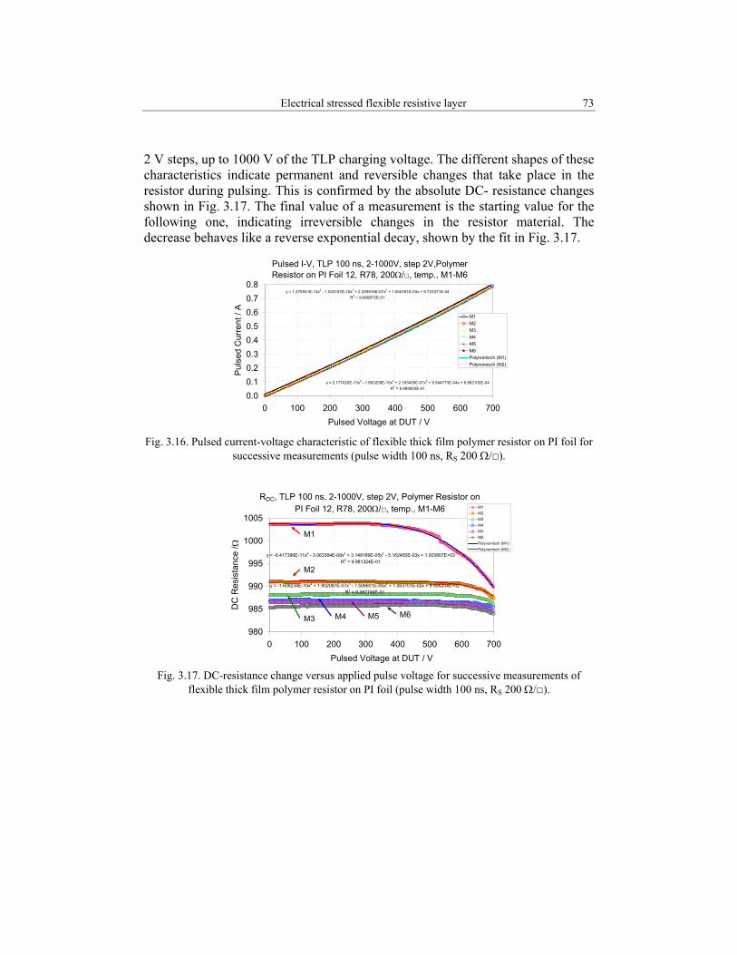
Applying successive pulses with stepwise increasing voltages, up to the same final, non destructive voltage, gives information about the irreversible changes that take place in the resistor. Fig. 3.16 depicts the pulsed current-voltage characteristic for six successive measurements, M1 – M6. During each measurement the amplitude of the 100 ns wide pulses was stepwise increased, in
Electrical stressed flexible resistive layer 73
2 V steps, up to 1000 V of the TLP charging voltage. The different shapes of these characteristics indicate permanent and reversible changes that take place in the resistor during pulsing. This is confirmed by the absolute DC- resistance changes shown in Fig. 3.17. The final value of a measurement is the starting value for the following one, indicating irreversible changes in the resistor material. The decrease behaves like a reverse exponential decay, shown by the fit in Fig. 3.17.
Pulsed I-V, TLP 100 ns, 2-1000V, step 2V,Polymer Resistor on PI Foil 12, R78, 200Ω/□, temp., M1-M6
0 100 200 300 400 500 600 700Pulsed Voltage at DUT / V
DC
Res
ista
nce
/ Ω
M1M2M3M4M5M6Polynomisch (M1)Polynomisch (M2)
M1
M2
M3 M4 M5 M6
Fig. 3.17. DC-resistance change versus applied pulse voltage for successive measurements of
flexible thick film polymer resistor on PI foil (pulse width 100 ns, RS 200 Ω/□).
74 Detlef Bonfert, Paul Svasta, Ciprian Ionescu
DC-Resistance, TLP 100 ns, Resistor 100Ω, Carbon on Al2O3
98.2598.5098.75
99.0099.2599.5099.75
100.00100.25
0 100 200 300 400 500 600 700Pulsed Voltage at DUT / V
DC
Res
ista
nce
/ Ω
M1M2M3M4M5M6
M1
M2 M3 M4 M5 M6
Fig. 3.18. DC-resistance change versus applied pulse voltage for successive measurements of thick
film polymer resistor on Al2O3 substrate (pulse width 100 ns, RS 100 Ω/□). Reference measurements of test structures on a rigid substrate of Al2O3. Fig. 3.18 shows that the resistive layer has a similar behavior as on the flexible substrate, the inorganic substrate does not influence the pulsed behavior because of the adiabatic regime of the stressing.
Rpulsed , TLP 100 ns, 2-1000V, step 2V, Polymer Resistor on PI Foil 12, ESL 12112, R78, 200Ω/□, temp. M1-M6
0 100 200 300 400 500 600 700Pulsed Voltage at DUT / V
Pul
sed
Res
ista
nce
/ Ω
M1M2M3M4M5M6
M1 M2M3
M4
M6
M5
Fig. 3.20. Pulsed resistance change versus applied pulse voltage for successive measurements of
thick film polymer resistor on Al2O3 (pulse width 100 ns, RS 100 Ω/□). From the corresponding pulsed I-V characteristic the R-V data during the
pulses were calculated and represented in Fig. 3.19., for polyimide substrate, and in Fig. 3.20 for the reference on Al2O3 substrate. The resistance decrease during pulsing indicates, besides the irreversible resistance change, dynamic effects, which are reversible after each measurement. The starting points for the successive measurements have the same variation as for the DC- spot measurements and confirm the irreversible changes in the resistive layer.
3.2.3 Influence of pulse number on resistance
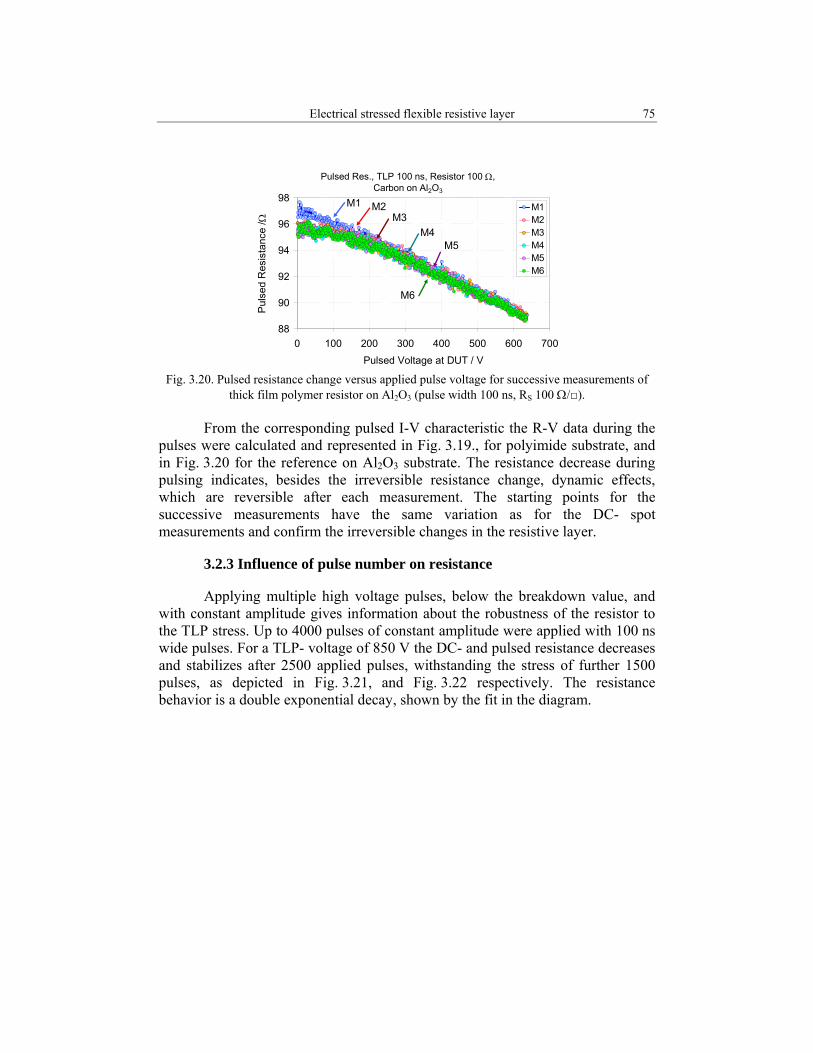
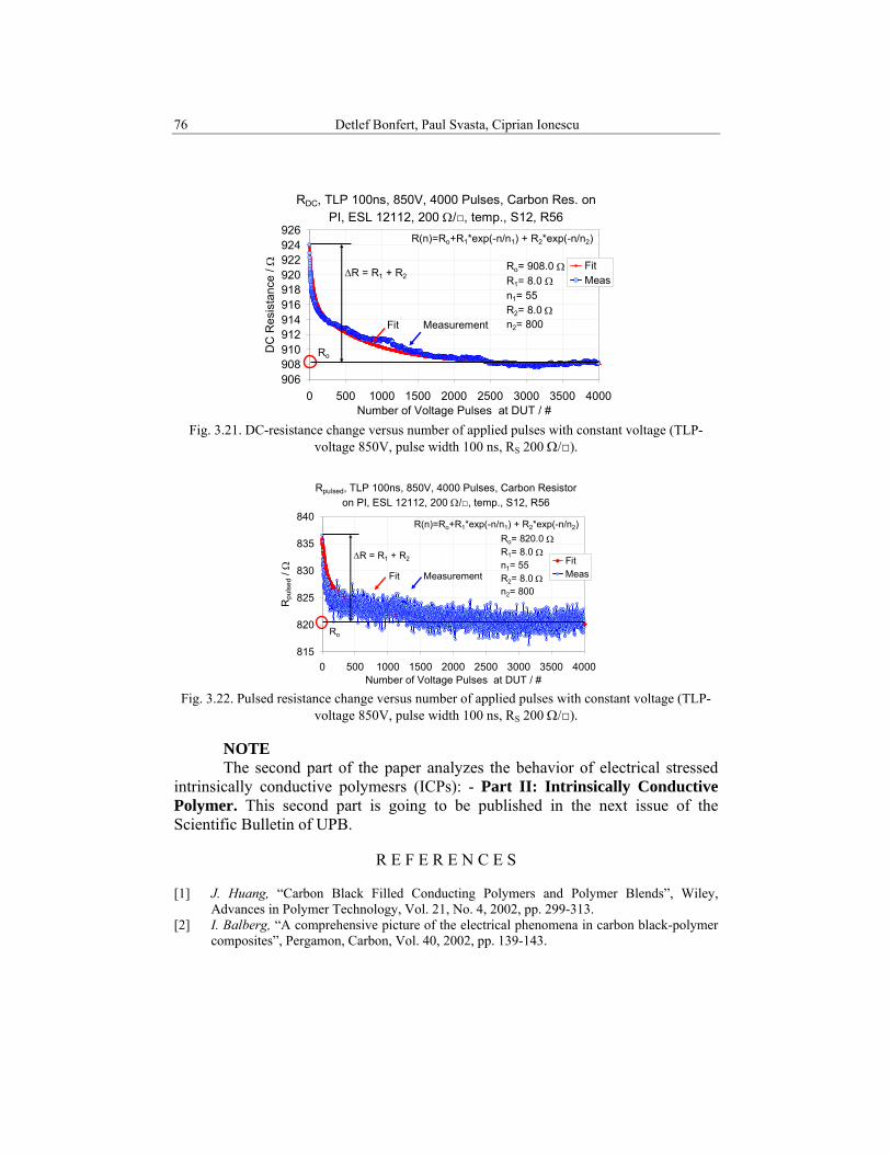
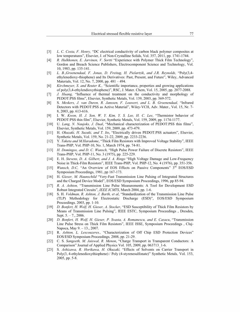
Applying multiple high voltage pulses, below the breakdown value, and with constant amplitude gives information about the robustness of the resistor to the TLP stress. Up to 4000 pulses of constant amplitude were applied with 100 ns wide pulses. For a TLP- voltage of 850 V the DC- and pulsed resistance decreases and stabilizes after 2500 applied pulses, withstanding the stress of further 1500 pulses, as depicted in Fig. 3.21, and Fig. 3.22 respectively. The resistance behavior is a double exponential decay, shown by the fit in the diagram.
0 500 1000 1500 2000 2500 3000 3500 4000Number of Voltage Pulses at DUT / #
Rpu
lsed
/ Ω Fit
Meas
R(n)=Ro+R1*exp(-n/n1) + R2*exp(-n/n2)
Ro
∆R = R1 + R2
MeasurementFit
Ro= 820.0 ΩR1= 8.0 Ωn1= 55R2= 8.0 Ωn2= 800
Fig. 3.22. Pulsed resistance change versus number of applied pulses with constant voltage (TLP-
voltage 850V, pulse width 100 ns, RS 200 Ω/□).
NOTE The second part of the paper analyzes the behavior of electrical stressed
intrinsically conductive polymesrs (ICPs): - Part II: Intrinsically Conductive Polymer. This second part is going to be published in the next issue of the Scientific Bulletin of UPB.
R E F E R E N C E S
[1] J. Huang, “Carbon Black Filled Conducting Polymers and Polymer Blends”, Wiley, Advances in Polymer Technology, Vol. 21, No. 4, 2002, pp. 299-313.
[2] I. Balberg, “A comprehensive picture of the electrical phenomena in carbon black-polymer composites”, Pergamon, Carbon, Vol. 40, 2002, pp. 139-143.
Electrical stressed flexible resistive layer 77
[3] L. C. Costa, F. Henry, “DC electrical conductivity of carbon black polymer composites at low temperatures”, Elsevier, J. of Non-Crystalline Solids, Vol. 357, 2011, pp. 1741-1744.
[4] R. Hulkkonen, E. Jarvinen, V. Sortti “Experience with Polymer Thick Film Technology”, Gordon and Breach Science Publishers, Electrocomponent Science and Technology, Vol. 10, 1983, pp. 135-141.
[5] L. B.,Groenendaal, F. Jonas, D. Freitag, H. Pielartzik, and J.R. Reynolds, “Poly(3,4-ethylenedioxy-thiophene) and Its Derivatives: Past, Present, and Future”, Wiley, Advanced Materials, Vol. 12, No. 7, 2000, pp. 481 – 494.
[6] Kirchmeyer, S. and Reuter K., “Scientific importance, properties and growing applications of poly(3,4-ethylendioxythiophene)”, RSC, J. Mater. Chem, Vol. 15, 2005, pp. 2077-2088.
[7] J. Huang, “Influence of thermal treatment on the conductivity and morphology of PEDOT:PSS films”, Elsevier, Synthetic Metals, Vol. 139, 2003, pp. 569-572.
[8] S. Meskers, J. van Duren, R. Janssen, F. Louwert, and L. B. Groenendaal, “Infrared Detectors with PEDOT:PSS as Active Material”, Wiley-VCH, Adv. Mater., Vol. 15, Nr. 7-8, 2003, pp. 613-616.
[9] I. W. Kwon, H. J. Son, W. Y. Kim, Y. S. Lee, H. C. Lee, “Thermistor behavior of PEDOT:PSS thin film”, Elsevier, Synthetic Metals, Vol. 159, 2009, pp. 1174-1177.
[10] U. Lang, N. Naujoks, J. Dual, “Mechanical characterization of PEDOT:PSS thin films”, Elsevier, Synthetic Metals, Vol. 159, 2009, pp. 473-479.
[11] H. Okuzaki, H. Suzuki, and T. Ito, “Electrically driven PEDOT:PSS actuators”, Elsevier, Synthetic Metals, Vol. 159, No. 21-22, 2009, pp. 2233-2236.
[12] Y. Taketa and M.Haradome, “Thick Film Resistors with Improved Voltage Stability”, IEEE Trans-PHP, Vol. PHP-10, No. 1, March 1974, pp. 74-81.
[13] H. Domingos, and D. C. Wunsch, “High Pulse Power Failure of Discrete Resistors”, IEEE Trans-PHP, Vol. PHP-11, No. 3 (1975), pp. 225-229.
[14] E. H. Stevens, D. A. Gilbert, and J. A. Ringo “High Voltage Damage and Low-Frequency Noise in Thick-Film Resistors”, IEEE Trans-PHP, Vol. PHP-12, No. 4 (1976), pp. 351-356.
[15] Wunsch, D.C, “An Overview of EOS Effects on Passive Components” 3rd EOS/ESD Symposium Proceedings, 1981, pp 167-173.
[16] H. Gieser, M. Haunschild “Very-Fast Transmission Line Pulsing of Integrated Structures and the Charged Device Model”, EOS/ESD Symposium Proceedings, 1996, pp 85-94.
[17] R. A. Ashton, “Transmission Line Pulse Measurements: A Tool for Development ESD Robust Integrated Circuits”, IEEE ICMTS, March 2004, pp. 1-6.
[18] S. H. Voldman, R. Ashton, J. Barth, et al, “Standardization of the Transmission Line Pulse (TLP) Methodology for Electrostatic Discharge (ESD)”, EOS/ESD Symposium Proceedings, 2003, pp. 1-10.
[19] D. Bonfert, H. Wolf, H. Gieser, A. Stocker, “ESD Susceptibility of Thick Film Resistors by Means of Transmission Line Pulsing”, IEEE ESTC, Symposium Proceedings , Dresden, Sept. 5. – 7., 2006.
[20] D. Bonfert, H. Wolf, H. Gieser, P. Svasta, A. Romanescu, and E. Cazacu, “Transmission Line Pulse Stress on Thick Film Resistors”, IEEE ISSE, Symposium Proceedings , Cluj-Napoca, May 9. – 13., 2007.
[21] R. Ashton, L. Lescouzeres., “Characterization of Off Chip ESD Protection Devices” EOS/ESD Symposium Proceedings, 2008, pp. 21-29.
[22] C. S. Sangeeth, M. Jaiswal, R. Menon, “Charge Transport in Transparent Conductors: A Comparison” Journal of Applied Physics Vol. 105, 2009, pp. 063713_1-6.
[23] S. Ashizawa, R. Horikawa, H. Okuzaki, “Effects of Solvents on Carrier Transport in Poly(3, 4-ethylenedioxythiophene) / Poly (4-styrenesulfonate)” Synthetic Metals, Vol. 153, 2005, pp. 5-8.
78 Detlef Bonfert, Paul Svasta, Ciprian Ionescu
[24] S. Meskers, K. J. van Duren, R. Janssen, “Non-linearity in the I-V characteristic of PEDOT:PSS due to Joule heating”, Elsevier, Organic electronics, Vol. 5, 2004, pp. 207-211.
[25] E. Vitoratos, E., S. Sakkopoulos, E. Dalas, N. Paliatsas, et. al, “Thermal degradation mechanism of PEDOT:PSS”, Elsevier, Organic Electronics, Vol. 10, 2009, pp. 61-66.
[26] A. Dziedzic, J. Kita, P. Mach, “Voltage nonlinearity of carbon black/polyesterimide thick resistive films”, Elsevier, Vacuum, Vol. 50, No. 1-2, 1998, pp. 125-130.
[27] T.B. Narayana, K. Ramkumar, M. Satyam, “Mechanism for downward trimming of polymer resistors”, J. of Applied Physics, Vol. 25, 1992, pp. 717-721.
[28] J. Nicolics, M. Mündlein, G. Hanreich, A. Zluc, H. Stahr, M. Franz, “Thermal Analysis of Multilayer Printed Circuit Boards with Embedded Carbon Black-Polymer Resistors”, IEEE 30th ISSE, 2007, pp. 46-52.
[29] D. Ortolino, J. Kita, R. Wurm, E. Blum, K. Beart, R. Moos, “Investigation of the short-time high-current behavior of vias manufactured in hybrid thick-film technology”, Elsevier, Microelectronics Reliability, Vol. 51, No. 7, July 2011, pp. 1257-1263.
[30] J. Ouyang, et al., “Mechanism of Conductivity Enhancement in PEDOT:PSS Film through Solvent treatment”, Elsevier, Polymer, Vol. 45, 2004, pp. 8443 – 8450.
[31] N. D. Sankir, “Selective deposition of PEDOT/PSS on to flexible substrates and tailoring the electrical resistivity by post treatment”, Emerald Group, Circuit World, Vol. 34, No. 4, 2008, pp. 32-37.
[32] Y. Srinivasa Rao,M. Satyam, “Dielectrophoretic mechanism for downward trimming of polymer resistors”, Emerald Group, Microelectronics International, Vol. 20, No. 2, 2003, pp. 10-15.
[33] Y. Srinivasa Rao, “Studies on temperature coefficient of resistance (TCR) of polymer thick film resistors”, Emerald Group, Microelectronics International, Vol. 25, No. 3, 2008, pp. 33-36.
[34] R. R. Brynsvold, and K. Manning, “Constant- Current Stressing of SiCr- Based Thin- Film Resistors: Initial “Wearout” Investigations”, IEEE Trans. Device and Materials Reliability, Vol. 7, No. 2, June 2007, pp. 259-269.
[35] G. C. Psarras, “Charge Transport Properties in Carbon Black/Polymer Composites”, J. of Polymer Science: Part B: Polymer Physics, Vol. 45, 2007, pp. 2535-2545.