General Description The MAX86150 is an integrated electrocardiogram, pulse oximeter, heart rate monitor sensor module. It includes internal LEDs, photodetectors, IR sensor and low-noise electronics with ambient light rejection. Maxim’s proprietary technology also includes robust algorithms to give meaningful outputs to the user with minimal additional design required. The MAX86150 helps ease design-in to mobile and wearable devices. The MAX86150 operates on a 1.8V supply voltage with a separate power supply for the internal LEDs. Communication to and from the module is entirely through a standard I 2 C-compatible interface. The module can be shut down through software with near zero standby current, allowing the power rails to remain powered at all times. Applications ● Smartphones ● Tablets ● Wearable Devices ● Fitness Assistant Devices Benefits and Features ● Electrocardiogram (ECG) Optimized for Dry Electrode Operation ● Reflective Heart Rate Monitor and Medical-Grade Pulse Oximeter ● Miniature 3.3mm x 5.6mm x 1.3mm 22-pin Optical Module • Optical-Grade Glass for Long-Term Optimal and Robust Performance ● Ultra-Low Power Operation for Mobile Devices • Ultra-Low Shutdown Current (0.7μA Typical) ● Robust Motion Artifact Resilience (Heart Rate Monitor) • High SNR and Robust Motion Rejection Algorithm ● -40°C to +85°C Operating Temperature Range Ordering Information appears at end of data sheet. 19-8402; Rev 1; 11/16 MAX86150 Integrated Photoplethysmogram and Electrocardiogram Bio-Sensor Module For Mobile Health Simplified Block Diagram HARDWARE FRAMEWORK PACKAGING OPTICAL I 2 C ELECTRICAL APPLICATIONS DRIVER HOST (AP) ALGORITHMS MAX86150 LED DRIVERS RED/IR LEDS DIGITAL NOISE CANCELLATION DATA FIFO 19-BIT ADC PHOTODIODE AMBIENT LIGHT CANCELLATION AFE ELECTRODES LEFT HAND RIGHT HAND HUMAN FINGER AMBIENT LIGHT GLASS LID 18-BIT ADC EVALUATION KIT AVAILABLE
Transcript
General DescriptionThe MAX86150 is an integrated electrocardiogram, pulse oximeter, heart rate monitor sensor module. It includes internal LEDs, photodetectors, IR sensor and low-noise electronics with ambient light rejection. Maxim’s proprietary technology also includes robust algorithms to give meaningful outputs to the user with minimal additional design required. The MAX86150 helps ease design-in to mobile and wearable devices.The MAX86150 operates on a 1.8V supply voltage with a separate power supply for the internal LEDs. Communication to and from the module is entirely through a standard I2C-compatible interface. The module can be shut down through software with near zero standby current, allowing the power rails to remain powered at all times.
VDD_ANA to GND_ANA ........................................-0.3V to +2.2VVDD_DIG to GND DIG ..........................................-0.3V to +2.2VVDD_ANA to VDD_DIG ..................................... VDD_DIG - 0.3V to
VDD_DIG + 0.3VGND_ANA to GND_DIG ............................... GND_DIG - 0.3V to
GND_DIG + 0.3VPGND to GND_ANA .............................................-0.3V to +0.3VLED_DRVx, VLED to PGND .................................-0.3V to +6.0VECG_P, ECG_N, ECG_C to GND_ANA ..............-0.3V to +2.2VC1_P, C1_N to GND_ANA ...................................-0.3V to +2.2VIDRV_P, IDRV_N to GND_ANA ...........................-0.3V to +2.2VVREF to GND_ANA ..............................................-0.3V to +2.2V
Output Short-Circuit Duration ....................................ContinuousContinuous Input Current Into Any Pin
(except LED_DRVx pins) ..............................................±20mAContinuous Power Dissipation
(derate 5.5mW/°C above +70°C) ................................440mWSDA, SCL, INTB, GPIO to GND_ANA .................-0.3V to +6.0VOESIP (derate 5.5mW/°C above +70°C) .............-40°C to 85°COperating Temperature Range ........................... -40°C to +85°CJunction Temperature ......................................................+150°CStorage Temperature Range ............................ -40°C to +105°CSoldering Temperature (reflow) .......................................+260°C
PACKAGE CODE F223A5+1Outline Number 21-100071Land Pattern Number 90-100024Thermal Resistance, Single Layer Board:Junction-to-Ambient (θJA) N/AJunction-to-Case Thermal Resistance (θJC) N/AThermal Resistance, Four Layer Board:Junction-to-Ambient (θJA) 180°C/WJunction-to-Case Thermal Resistance (θJC) 150°C/W
www.maximintegrated.com Maxim Integrated 5
MAX86150 Integrated Photoplethysmogram and Electrocardiogram Bio-Sensor Module For
Mobile Health
Package thermal resistances were obtained using the method described in JEDEC specification JESD51-7, using a four-layer board. For detailed information on package thermal considerations, refer to www.maximintegrated.com/thermal-tutorial.
Absolute Maximum Ratings
Stresses beyond those listed under “Absolute Maximum Ratings” may cause permanent damage to the device. These are stress ratings only, and functional operation of the device at these or any other conditions beyond those indicated in the operational sections of the specifications is not implied. Exposure to absolute maximum rating conditions for extended periods may affect device reliability.
Package Information
For the latest package outline information and land patterns (footprints), go to www.maximintegrated.com/packages. Note that a “+”, “#”, or “-” in the package code indicates RoHS status only. Package drawings may show a different suffix character, but the drawing pertains to the package regardless of RoHS status.
MAX86150 Integrated Photoplethysmogram and Electrocardiogram Bio-Sensor Module For
Mobile Health
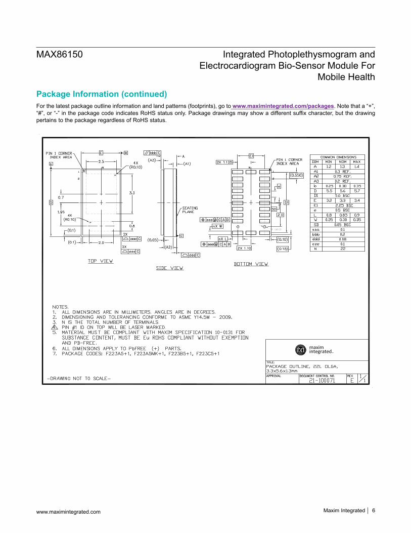
Package Information (continued)For the latest package outline information and land patterns (footprints), go to www.maximintegrated.com/packages. Note that a “+”, “#”, or “-” in the package code indicates RoHS status only. Package drawings may show a different suffix character, but the drawing pertains to the package regardless of RoHS status.
MAX86150 Integrated Photoplethysmogram and Electrocardiogram Bio-Sensor Module For
Mobile Health
Package Information (continued)For the latest package outline information and land patterns (footprints), go to www.maximintegrated.com/packages. Note that a “+”, “#”, or “-” in the package code indicates RoHS status only. Package drawings may show a different suffix character, but the drawing pertains to the package regardless of RoHS status.
(VDD_ANA = VDD_DIG = 1.8V, VLED = 3.3V, VGND_ANA = VGND_DIG = VPGND = 0V, TA = +25°C, min/max are from TA = -40°C to +85°C, unless otherwise noted.) (Note 1)
PARAMETER SYMBOL CONDITIONS MIN TYP MAX UNITSPOWER SUPPLYPower Supply Voltage VDD Guaranteed by RED and IR count tolerance 1.7 1.8 2.0 VLED Supply Voltage VLED Guaranteed by PSRR of LED driver 3.1 3.3 5 V
Input Leakage Current IINVIN = 0V, TA = +25°C (SDA, SCL) 0.01 1
μAVIN = VDD, TA = +25°C (SDA, SCL) 0.01 1
I2C TIMING CHARACTERISTICS (SDA, SCL) (Note 3, Figure 1)I2C Write Address BC HexI2C Read Address BD HexSerial Clock Frequency fSCL 0 400 kHzBus Free Time Between STOP and START Conditions
tBUF 1.3 µs
Hold Time (Repeated) START Condition tHD,STA 0.6 µs
SCL Pulse-Width Low tLOW 1.3 µsSCL Pulse-Width High tHIGH 0.6 µsSetup Time for a Repeated START Condition tSU,STA 0.6 µs
Data Hold Time tHD,DAT 0 900 nsData Setup Time tSU,DAT 100 nsSetup Time for STOP Condition tSU,STO 0.6 µs
Pulse Width of Suppressed Spike tSP 0 50 ns
Bus Capacitance CB 400 pFSDA and SCL Receiving Rise Time tR
20 + 0.1CB
300 ns
SDA and SCL Receiving Fall Time tF
20 + 0.1CB
300 ns
SDA Transmitting Fall Time tF
20 + 0.1CB
300 ns
(VDD_ANA = VDD_DIG = 1.8V, VLED = 3.3V, VGND_ANA = VGND_DIG = VPGND = 0V, TA = +25°C, min/max are from TA = -40°C to +85°C, unless otherwise noted.) (Note 1)
www.maximintegrated.com Maxim Integrated 10
MAX86150 Integrated Photoplethysmogram and Electrocardiogram Bio-Sensor Module For
Mobile Health
Electrical Characteristics (continued)
Note 1: All devices are 100% production tested at TA = +25°C. Specifications over temperature limits are guaranteed by Maxim Integrated’s bench or proprietary automated test equipment (ATE) characterization.
Note 2: Specifications are guaranteed by Maxim Integrated’s bench characterization and by 100% production test using proprietary ATE setup and conditions.
Note 3: For design guidance only. Not production tested.Note 4: Test conditions: SPS = 1600Hz, ECG_ADC_OSR[1:0] = 00 (OSR = 16), ECG_ADC_CLK = 0 (25.6kHZ), IA_GAIN[1:0] = 01
(IA_GAIN = 9.5), and PGA_ECG_GAIN[1:0] = 11 (PGA_GAIN = 8), unless otherwise noted.Note 5: For measurements with DC difference as input, the highpass filter function is disabled.Note 6: Internal reference only.
(VDD_ANA = VDD_DIG = 1.8V, VLED = 3.3V, VGND_ANA = VGND_DIG = VPGND = 0V, TA = +25°C, min/max are from TA = -40°C to +85°C, unless otherwise noted.) (Note 1)
Electrical Characteristics (continued)
Figure 1. I2C-Compatible Interface Timing Diagram
www.maximintegrated.com Maxim Integrated 11
MAX86150 Integrated Photoplethysmogram and Electrocardiogram Bio-Sensor Module For
Mobile Health
SDA
SCL
tHD,STA
START CONDITIONtR tF
tLOWtSU,DAT
tHD,DAT
tSU,STAtHD,STA
REPEATED START CONDITION
tSP tSU,STO
tBUF
STOPCONDITION
STARTCONDITION
tHIGH
(TA = +25°C, unless otherwise noted.)
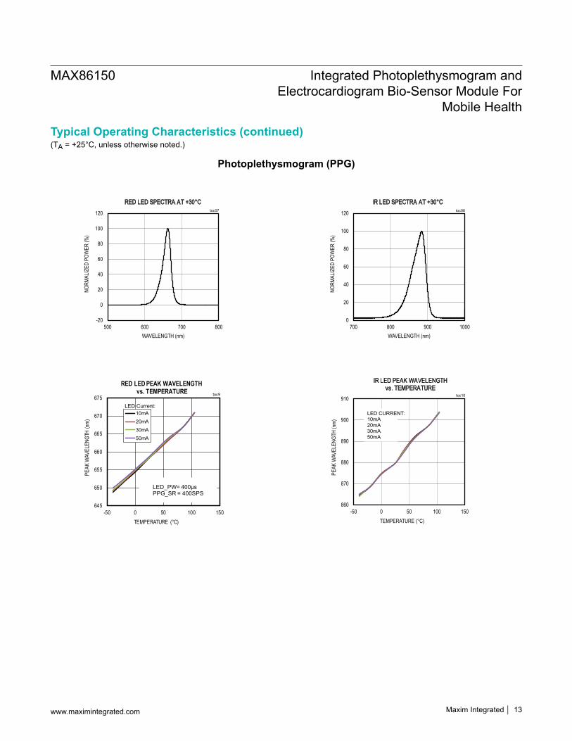
Photoplethysmogram (PPG)
0102030405060708090
100110
0 1 2 3 4 5
RED
LED
CURR
ENT
(mA)
VLED VOLTAGE (V)
RED LED SUPPLY HEADROOMtoc01
ILED = 20mA
VLED = VX_DRV ILED = 100mA
ILED = 50mA
0102030405060708090
100110
0 1 2 3 4 5IR
LED
CURR
ENT
(mA)
VLED VOLTAGE (V)
IR LED SUPPLY HEADROOMtoc02
ILED = 50mA
VLED = VX_DRV
ILED = 20mA
ILED = 100mA
0.0
0.1
0.2
0.3
0.4
0.5
0.6
0.7
0.8
0.9
1.0
0 0.5 1 1.5 2 2.5
SUPP
LY C
URRE
NT (m
A)
SUPPLY VOLTAGE (V)
SHUTDOWN MODE
IR MODE
SPO2 MODE
VDD SUPPLY CURRENT vs.SUPPLY VOLTAGE toc03
0
50000
100000
150000
200000
250000
0 5 10 15 20
COUN
TS (S
UM)
DISTANCE (mm)
DC COUNTS vs. DISTANCE FORWHITE HIGH IMPACT STYRENE CARD
toc04
RED
IR
LED_PW = 400µsPPG_SR = 400 SPSADC FULL SCALE = 16384nA
0.0
1.0
2.0
3.0
4.0
5.0
6.0
7.0
-50 0 50 100 150
V DD
SHUT
DOW
N CU
RREN
T (uA
)
TEMPERATURE (°C)
1.7V
1.8V
2.0V
2.2V
VDD SHUTDOWN CURRENTvs. TEMPERATURE toc05
VDD
0.06
0.07
0.08
0.09
0.10
0.11
0.12
0.13
0.14
-50 0 50 100 150
V LED
SHUT
DOW
N CU
RREN
T (u
A)
TEMPERATURE (°C)
VLED SHUTDOWN CURRENTvs. TEMPERATURE
VLED = 4.75V
toc06
VLED = 5.25V
Maxim Integrated 12www.maximintegrated.com
MAX86150 Integrated Photoplethysmogram and Electrocardiogram Bio-Sensor Module For
Mobile Health
Typical Operating Characteristics
Photoplethysmogram (PPG)
-20
0
20
40
60
80
100
120
500 600 700 800
NORM
ALIZ
ED P
OWER
(%)
WAVELENGTH (nm)
RED LED SPECTRA AT +30°Ctoc07
0
20
40
60
80
100
120
700 800 900 1000NO
RMAL
IZED
POW
ER (%
)WAVELENGTH (nm)
IR LED SPECTRA AT +30°Ctoc08
645
650
655
660
665
670
675
-50 0 50 100 150
PEAK
WAV
ELEN
GTH
(nm)
TEMPERATURE (°C)
10mA
20mA
30mA
50mA
RED LED PEAK WAVELENGTH vs. TEMPERATURE toc9
LED Current:
LED_PW= 400µsPPG_SR = 400SPS
860
870
880
890
900
910
-50 0 50 100 150
PEAK
WAV
ELEN
GTH
(nm)
TEMPERATURE (°C)
IR LED PEAK WAVELENGTHvs. TEMPERATURE
toc10
LED CURRENT:10mA20mA30mA50mA
Maxim Integrated 13www.maximintegrated.com
MAX86150 Integrated Photoplethysmogram and Electrocardiogram Bio-Sensor Module For
MAX86150 Integrated Photoplethysmogram and Electrocardiogram Bio-Sensor Module For
Mobile Health
Typical Operating Characteristics (continued)
(TA = +25°C, unless otherwise noted.)
Electrocardiogram (ECG)
Typical Operating Characteristics (continued)
Maxim Integrated 15www.maximintegrated.com
MAX86150 Integrated Photoplethysmogram and Electrocardiogram Bio-Sensor Module For
Mobile Health
0.45
0.50
0.55
0.60
0.65
0.70
-40 -15 10 35 60 85
COMM
ON M
ODE
VOLT
AGE
(v)
TEMPERATURE (°C)
100 MΩ
INPUT COMMON MODE VOLTAGE vs. TEMPERATURE
(ECG_P) toc 16
0.45
0.50
0.55
0.60
0.65
0.70
-40 -15 10 35 60 85CO
MMON
MOD
E VO
LTAG
E (V
)TEMPERATURE (°C)
100 MΩ
INPUT COMMON MODE VOLTAGE vs. TEMPERATURE
(ECG_N) toc 17
MAX86150
N.C. 1
N.C. 2
N.C. 3
ECG_N 4
ECG_P 5
6
7
8
N.C.
14
N.C.
15
16
GND_DIG17
GND_ANA18
VREF19
C1_N20
21
10
VDD_DIG
PGND
9
VLED
1211
22
N.C.
VDD_ANA
13
C1_P
N.C.
SDA
SCL
N.C.
INTB
www.maximintegrated.com Maxim Integrated 16
MAX86150 Integrated Photoplethysmogram and Electrocardiogram Bio-Sensor Module For
Mobile Health
Pin Configuration
PIN NAME FUNCTIONN.C.
1–3, 6, 10–12, 22 N.C. No Connection. Connect to an unconnected PCB pad for mechanical stability. N.C. pin should not
be connected to any signal, power, or ground pins.ECG
5 ECG_P Positive ECG Electrode4 ECG_N Negative ECG Electrode21 C1_P Capacitor for ECG HPF. Connect to C1_N through a 1μF capacitor.20 C1_N Capacitor for ECG HPF. Connect to C1_P through a 1μF capacitor.
POWER13 VDD_DIG Digital Logic Supply. Connect to externally regulated supply. Bypass to GND_DIG.17 GND_DIG Digital Logic and Digital Pad Return. Connect to GND.14 VDD_ANA Analog Supply. Connect to externally regulated supply. Bypass to GND_ANA.18 GND_ANA Analog Power Return. Connect to GND.15 VLED LED Power Supply Input. Connect to external battery supply. Bypass to PGND.16 PGND LED Power Return. Connect to GND.
REFERENCE19 VREF Internal Reference Decoupling Point. Bypass to GND_ANA.
www.maximintegrated.com Maxim Integrated 17
MAX86150 Integrated Photoplethysmogram and Electrocardiogram Bio-Sensor Module For
Mobile Health
Pin Description
Detailed DescriptionThe MAX86150 is a electrocardiogram, pulse oximetry, and heart rate sensor system solution module designed for the demanding requirements of mobile devices. The MAX86150 maintains a very small total solution size without sacrificing optical or electrical performance. Minimal external hardware components are necessary for integration into a mobile device. The MAX86150 is fully adjustable through software registers, and the digital output data is stored in a 32-deep FIFO within the device. The FIFO allows the MAX86150 to be connected to a microcontroller or processor on a shared bus, where the data is not being read continuously from the MAX86150’s registers.
SpO2 SubsystemThe SpO2 subsystem in the MAX86150 is composed of ambient light cancellation (ALC), a continuous-time sigma-delta ADC, and proprietary discrete time filter. The ALC has an internal DAC to cancel ambient light and increase the effective dynamic range. The internal ADC is a continuous time oversampling sigma delta converter with 19-bit resolution. The ADC output data rate can be programmed from 10sps (samples per second) to 3200sps. The MAX86150 includes a proprietary discrete time filter to reject 50Hz/60Hz interference and slow moving residual ambient noise.
www.maximintegrated.com Maxim Integrated 18
MAX86150 Integrated Photoplethysmogram and Electrocardiogram Bio-Sensor Module For
Mobile Health
VISIBLE + IRIR
N.C.
V LED
PGND
SDA
SCL
INT
LED DRIVERS
DIGITAL CONTROLLER
OR SIGNAL PROCESSOR
μCOR
APPLICATIONS PROCESSOR
1.8V
GND_ANA GND_DIG
1.8V
V DD_
DIG
V DD_
ANA
ECG_
P3.3V
RED
N.C.
ADC
ADC
ECG_
N
C1_P
C1_N
1μF
ECG
VREF
1μF
V REF
Functional Diagrams
LED DriverThe MAX86150 integrates red and infrared LED drivers to modulate LED pulses for SpO2 and HR measurements. The LED current can be programmed from 0mA to 100mA with proper VLED supply voltage. The LED pulse width can be programmed from 50μs to 400μs to allow the algorithm to optimize SpO2 and HR accuracy and power consumption based on use cases.
Proximity FunctionThe MAX86150 includes a proximity function to save power and reduce visible light emission when the user’s finger is not on the sensor. Proximity function is enabled by setting PROX_INT_EN to 1. When the SpO2 or HR function is initiated, the IR LED is turned on in proximity mode with a drive current set by the PILOT_PA register. When an object is detected by exceeding the IR ADC count threshold (set in the PROX_INT_ THRESH register), PROX_INT interrupt is asserted and the part transitions automatically to the normal SpO2/HR mode. To reenter PROX mode, a new SpO2 or HR reading must be initiated (even if the value is the same). The proximity function can be disabled by resetting PROX_INT_EN to 0. In that case, when the SpO2 or HR function is initiated in the FIFO Data Control registers, the SpO2 or HR mode begins immediately.
Electrocardiogram (ECG)The ECG subsystem in the MAX86150 is designed specifically for mobile applications. It features single-lead
ECG technology that is optimized for dry electrode operation. It comprises Maxim proprietary analog front end (AFE), which includes an 18-bit ADC. Figure 2 shows the ECG Subsystem Block Diagram. The primary function of the AFE is to digitize heart signals. This process is compli-cated by the need to reject interference from strong RF sources, common-mode line frequency, signals from other muscles, and electrical noise. The electrical connections to the patient must not create a shock hazard or interfere with other equipment that might be connected to the device. The ECG subsystem also includes an on-chip highpass filter, when coupled with the digital lowpass filter implemented in the algorithm, ensures high SNR in real applications. The ADC output data rate can be pro-grammed from 200sps (samples per second) to 3200sps.The output of the ADC is an 18-bit digital representation of the input voltage. Each data sample takes three bytes in the FIFO, and the data is right-justified and in bipolar two's-complement format.To calculate the equivalent differential input voltage of the ADC, the formula is as follows:
V_INPUT = ADC_CODE x 12.247μV/IA_GAIN/PGA_GAIN
where ADC_CODE is converted to a bipolar integer decimal format, which can be positive or negative. Note that only one gain setting, IA_GAIN = 9.5 and PGA_GAIN = 8, is trimmed to a tight tolerance at the factory, and the other gains are typical expected values only.
Figure 2. MAX86150 ECG Subsystem Block Diagram
www.maximintegrated.com Maxim Integrated 19
MAX86150 Integrated Photoplethysmogram and Electrocardiogram Bio-Sensor Module For
Mobile Health
AC-COULED INSTRUMENTATION AMPLIFIER
WITH CHOPPING
C1_P C1_N
ECG_P
ECG_N
COMMON-MODE AMPLIFIER
PGAΔΣ ADC
ADC CLOCK
DATAFIFO
INTB,SDA,SCL
0.6V
INTERNAL VREF
X X
1.56pF
20kΩ
1.56pF
20kΩ
1μF1μF
VREF
ADDRESS NAME MSB LSBStatus Registers
0x00 Interrupt Status 1[7:0] A_FULL_ PPG_RDY_ ALC_OVF_ PROX_
INT_ — — — PWR_RDY_
0x01 Interrupt Status 2[7:0] VDD_OOR_ — — — — ECG_
Field A_FULL PPG_RDY ALC_OVF PROX_INT — — — PWR_RDYReset 0x0 0x0 0x0 0x0 — — — 0x0Access Type Read Only Read Only Read Only Read Only — — — Read Only
A_FULL: FIFO Almost Full Flag
VALUE ENUMERATION DECODE0 OFF Normal Operation
1 ONIndicates that the FIFO buffer overflows the threshold set by FFIFO_A_FULL[3:0] on the next sample. This bit is cleared when the Interrupt Status 1 register is read. It is also cleared when FIFO_DATA register is read, if A_FULL_CLR = 1
PPG_RDY: New PPG FIFO Data Ready
VALUE ENUMERATION DECODE0 OFF Normal Operation
1 ONIn SpO2 and HR modes, this interrupt triggers when there is a new sample in the data FIFO. The interrupt is cleared by reading the Interrupt Status 1 register (0x00), or by reading the FIFO_DATA register.
ALC_OVF: Ambient Light Cancellation Overflow
VALUE ENUMERATION DECODE0 OFF Normal Operation
1 ONThis interrupt triggers when the ambient light cancellation function of the SpO2/HR photodiode has reached its maximum limit due to overflow, and therefore, ambient light is affecting the output of the ADC. The interrupt is cleared by reading the Interrupt Status 1 register (0x00).
www.maximintegrated.com Maxim Integrated 21
MAX86150 Integrated Photoplethysmogram and Electrocardiogram Bio-Sensor Module For
Mobile Health
PROX_INT: Proximity interruptIf PROX_INT is masked then the prox mode is disabled and the select PPG begins immediately. This bit is cleared when the Interrupt Status 1 Register is read.
VALUE ENUMERATION DECODE0 OFF Normal Operation1 ON Indicates that the proximity threshold has been crossed when in proximity mode.
PWR_RDY: Power Ready Flag
VALUE ENUMERATION DECODE0 OFF Normal Operation
1 ON Indicates that VBATT went below the UVLO threshold. This bit is not triggered by a soft reset. This bit is cleared when Interrupt Status 1 Register is read.
Interrupt Status 2 (0x01)BIT 7 6 5 4 3 2 1 0
Field VDD_OOR — — — — ECG_RDY — —Reset 0x0 — — — — 0x0 — —Access Type Read Only — — — — Read Only — —
VDD_OOR: VDD Out-of-Range FlagThis flag checks if the VDD_ANA supply voltage is outside supported range.
VALUE ENUMERATION DECODE0 OFF VDD_ANA between range.
1 ONIndicated that VDD_ANA is greater than 2.05V or less than 1.65V. This bit is automatically cleared when the Interrupt Status 2 register is read. The detection circuitry has a 10ms delay time and continues to trigger as long as the VDD_ANA is out of range.
ECG_RDY: New ECG FIFO Data ReadyThis flag checks if the VDD_ANA supply voltage is outside supported range.
VALUE ENUMERATION DECODE0 OFF Normal Operation1 ON Indicates that the ECG ADC has finished it’s existing conversion.
www.maximintegrated.com Maxim Integrated 22
MAX86150 Integrated Photoplethysmogram and Electrocardiogram Bio-Sensor Module For
VALUE ENUMERATION DECODE0 OFF A_FULL interrupt is disabled1 ON A_FULL interrupt is enabled
PPG_RDY_EN: New PPG FIFO Data Ready Interrupt enable
VALUE ENUMERATION DECODE0 OFF PPG_RDY interrupt is disabled1 ON PPG_RDY interrupt is enabled.
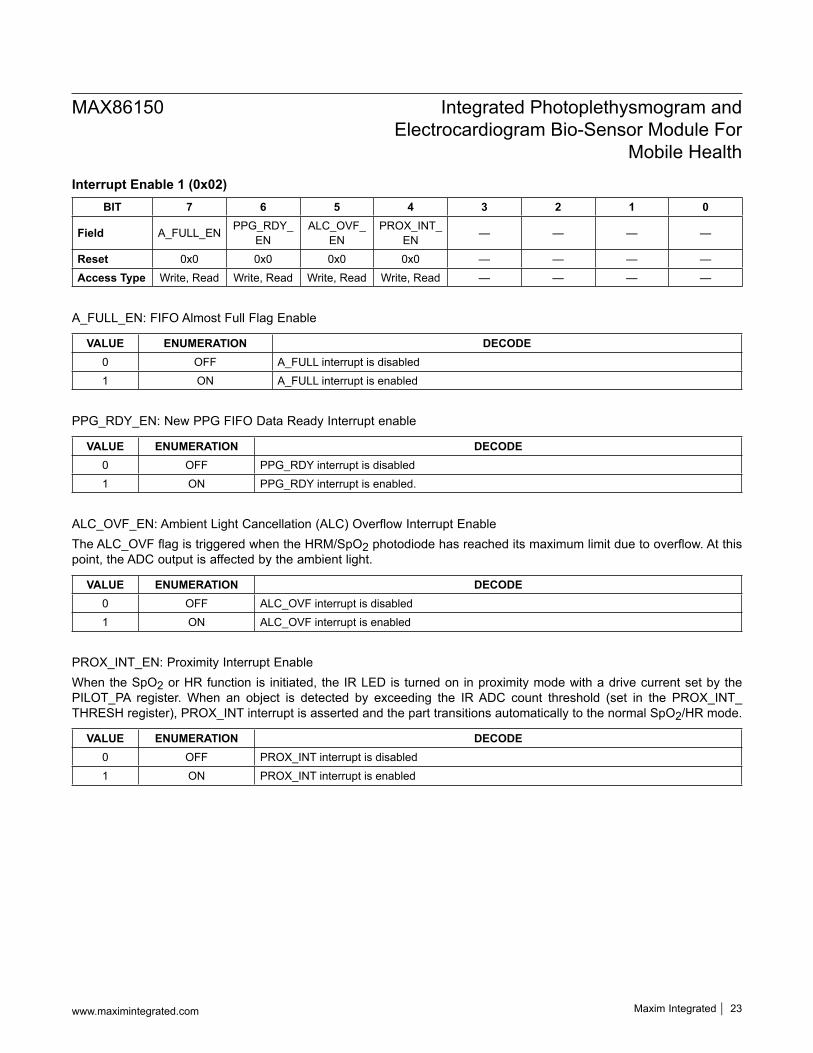
ALC_OVF_EN: Ambient Light Cancellation (ALC) Overflow Interrupt EnableThe ALC_OVF flag is triggered when the HRM/SpO2 photodiode has reached its maximum limit due to overflow. At this point, the ADC output is affected by the ambient light.
VALUE ENUMERATION DECODE0 OFF ALC_OVF interrupt is disabled1 ON ALC_OVF interrupt is enabled
PROX_INT_EN: Proximity Interrupt EnableWhen the SpO2 or HR function is initiated, the IR LED is turned on in proximity mode with a drive current set by the PILOT_PA register. When an object is detected by exceeding the IR ADC count threshold (set in the PROX_INT_ THRESH register), PROX_INT interrupt is asserted and the part transitions automatically to the normal SpO2/HR mode.
VALUE ENUMERATION DECODE0 OFF PROX_INT interrupt is disabled1 ON PROX_INT interrupt is enabled
www.maximintegrated.com Maxim Integrated 23
MAX86150 Integrated Photoplethysmogram and Electrocardiogram Bio-Sensor Module For
VALUE ENUMERATION DECODE0 OFF Disables the VDD_OVR interrupt1 ON Enables the VDD_OVR interrupt
ECG_RDY_EN: New ECG FIFO Data Ready Interrupt Enable
VALUE ENUMERATION DECODE0 OFF ECG_RDY interrupt is disabled1 ON ECG_RDY interrupt is enabled
FIFO Write Pointer (0x04)BIT 7 6 5 4 3 2 1 0
Field — — — FIFO_WR_PTR[4:0]Reset — — — 0x00Access Type — — — Write, Read
FIFO_WR_PTR: FIFO Write PointerThis points to the location where the next sample is written. This pointer advances for each sample pushed on to the FIFO.
www.maximintegrated.com Maxim Integrated 24
MAX86150 Integrated Photoplethysmogram and Electrocardiogram Bio-Sensor Module For
Mobile Health
Overflow Counter (0x05)BIT 7 6 5 4 3 2 1 0
Field — — — OVF_COUNTER[4:0]Reset — — — 0x00Access Type — — — Read Only
OVF_COUNTER: FIFO Overflow CounterWhen FIFO is full, any new samples result in new or old samples getting lost depending on FIFO_ROLLS_ON_FULL. OVF_COUNTER counts the number of samples lost. It saturates at 0x1F.
FIFO Read Pointer (0x06)BIT 7 6 5 4 3 2 1 0
Field — — — FIFO_RD_PTR[4:0]Reset — — — 0x00Access Type — — — Write, Read
FIFO_RD_PTR: FIFO Read PointerThe FIFO Read Pointer points to the location from where the processor gets the next sample from the FIFO through the I2C interface. This advances each time a sample is popped from the FIFO. The processor can also write to this pointer after reading the samples. This allows rereading (or retrying) samples from the FIFO.
www.maximintegrated.com Maxim Integrated 25
MAX86150 Integrated Photoplethysmogram and Electrocardiogram Bio-Sensor Module For
Mobile Health
FIFO Data Register (0x07)BIT 7 6 5 4 3 2 1 0
Field FIFO_DATA[7:0]Reset 0x00Access Type Write, Read
FIFO_DATA: FIFO Data RegisterThis is a read-only register and is used to get data from the FIFO. See FIFO Description for more details.
A_FULL_CLR: FIFO Almost Full Interrupt OptionsThis defines whether the A-FULL interrupt should get cleared by FIFO_DATA register read.
VALUE ENUMERATION DECODE
0 RD_DATA_NOCLR A_FULL interrupt does not get cleared by FIFO_DATA register read. It gets cleared by status register read.
1 RD_DATA_CLR A_FULL interrupt gets cleared by FIFO_DATA register read or status register read.
A_FULL_TYPE: FIFO Almost Full Flag OptionsThis defines the behavior of the A_FULL interrupt.
VALUE ENUMERATION DECODE
0 AFULL_RPT A_FULL interrupt gets asserted when the a_full condition is detected. It is cleared by status register read, but re-asserts for every sample if the a_full condition persists.
1 AFULL_ONCEA_FULL interrupt gets asserted only when the a_full condition is detected. The interrupt gets cleared on status register read, and does not re-assert for every sample until a new a-full condition is detected.
www.maximintegrated.com Maxim Integrated 26
MAX86150 Integrated Photoplethysmogram and Electrocardiogram Bio-Sensor Module For
Mobile Health
FIFO_ROLLS_ON_FULL: FIFO Rolls on Full OptionsThis bit controls the behavior of the FIFO when the FIFO becomes completely filled with data. When the device is in PROX mode, the FIFO always rolls on full.
Push to FIFO is enabled when FIFO is full if FIFO_ROLLS_ON_FULL = 1 and old samples are lost. Both FIFO_WR_PTR and FIFO_RD_PTR increment for each sample after the FIFO is full.
Push to FIFO is disabled when FIFO is full if FIFO_ROLLS_ON_FULL = 0 and new samples are lost. FIFO_WR_PTR does not increment for each sample after the FIFO is full.
VALUE ENUMERATION DECODE
0 OFF The FIFO stops on full.
1 ON The FIFO automatically rolls over on full.
FIFO_A_FULL: FIFO Almost Full ValueThese bits indicate how many new samples can be written to the FIFO before the interrupt is asserted. For example, if set to 0xF, the interrupt triggers when there is 17 empty space left (15 data samples), and so on.
FIFO_A_FULL<3:0> FREE SPACE BEFORE INTERRUPT # OF SAMPLES IN FIFO
0000 0 32
0001 1 31
0010 2 30
0011 3 29
---- ---- ----
1110 14 18
1111 15 17
www.maximintegrated.com Maxim Integrated 27
MAX86150 Integrated Photoplethysmogram and Electrocardiogram Bio-Sensor Module For
Mobile Health
FIFO Data Control Register 1 (0x09)BIT 7 6 5 4 3 2 1 0
Field FD2[3:0] FD1[3:0]Reset 0x0 0x0Access Type Write, Read Write, Read
FD2: FIFO Data Time Slot 2These bits set the data type for element 2 of the FIFO.
The FIFO can hold up to 32 samples. Each sample can hold up to four elements and each element is 3 bytes wide. The data type that gets stored in the 3 bytes is configured by FD1, FD2, FD3 and FD4 according to the following table. For restriction on data type sequences, see the FIFO Description section.
FD2[3:0] DATA TYPE FD2[3:0] DATA TYPE FD2[3:0] DATA TYPE FD2[3:0] DATA TYPE0000 None 0100 Reserved 1000 Reserved 1100 Reserved0001 PPG_LED1 0101 Pilot LED1 1001 ECG 1101 Reserved0010 PPG_LED2 0110 Pilot LED2 1010 Reserved 1110 Reserved0011 Reserved Reserved Pilot LED3 1011 Reserved 1111 Reserved
FD1: FIFO Data Time Slot 1These bits set the data type for element 1 of the FIFO.
The FIFO can hold up to 32 samples. Each sample can hold up to four elements and each element is 3 bytes wide. The data type that gets stored in the 3 bytes is configured by FD1, FD2, FD3 and FD4 according to the following table. For restriction on data type sequences, see the FIFO Description section.
FD1[3:0] DATA TYPE FD1[3:0] DATA TYPE FD1[3:0] DATA TYPE FD1[3:0] DATA TYPE0000 None 0100 Reserved 1000 Reserved 1100 Reserved0001 PPG_LED1 0101 Pilot LED1 1001 ECG 1101 Reserved0010 PPG_LED2 0110 Pilot LED2 1010 Reserved 1110 Reserved0011 Reserved 0111 Reserved 1011 Reserved 1111 Reserved
www.maximintegrated.com Maxim Integrated 28
MAX86150 Integrated Photoplethysmogram and Electrocardiogram Bio-Sensor Module For
Mobile Health
FIFO Data Control Register 2 (0x0A)BIT 7 6 5 4 3 2 1 0
Field FD4[3:0] FD3[3:0]Reset 0x0 0x0Access Type Write, Read Write, Read
FD4: FIFO Data Time Slot 4These bits set the data type for element 4 of the FIFO.
The FIFO can hold up to 32 samples. Each sample can hold up to four elements and each element is 3 bytes wide. The data type that gets stored in the 3 bytes is configured by FD1, FD2, FD3 and FD4 according to the following table. For restriction on data type sequences, see the FIFO Description section.
FD4[3:0] DATA TYPE FD4<3:0> DATA TYPE FD4<3:0> DATA TYPE FD4<3:0> DATA TYPE0000 None 0100 Reserved 1000 Reserved 1100 Reserved0001 PPG_LED1 0101 Pilot LED1 1001 ECG 1101 Reserved0010 PPG_LED2 0110 Pilot LED2 1010 Reserved 1110 Reserved0011 Reserved 0111 Reserved 1011 Reserved 1111 Reserved
FD3: FIFO Data Time Slot 3These bits set the data type for element 3 of the FIFO.
The FIFO can hold up to 32 samples. Each sample can hold up to four elements and each element is 3 bytes wide. The data type that gets stored in the 3 bytes is configured by FD1, FD2, FD3 and FD4 according to the following table. For restriction on data type sequences please refer to the FIFO Description section.
FD3[3:0] DATA TYPE FD3<3:0> DATA TYPE FD3<3:0> DATA TYPE FD3<3:0> DATA TYPE0000 None 0100 Reserved 1000 Reserved 1100 Reserved0001 PPG_LED1 0101 Pilot LED1 1001 ECG 1101 Reserved0010 PPG_LED2 0110 Pilot LED2 1010 Reserved 1110 Reserved0011 Reserved 0111 Reserved 1011 Reserved 1111 Reserved
www.maximintegrated.com Maxim Integrated 29
MAX86150 Integrated Photoplethysmogram and Electrocardiogram Bio-Sensor Module For
0 OFF Push to FIFO is disabled, but the read and write pointers and the data in the FIFO are all held at their values before FIFO_EN is set to 0.
1 ON The FIFO is enabled. When this bit is set the FIFO is flushed of all old data and the new samples start loading from pointer zero.
SHDN: Shutdown ControlThe part can be put into a power-save mode by setting this bit to one. While in power-save mode, all registers retain their values, and write/read operations function as normal. All interrupts are cleared to zero in this mode.
VALUE ENUMERATION DECODE0 OFF The part is in normal operation. No action taken.
1 ON
The part can be put into a power-save mode by writing a ‘1’ to this bit. While in this mode all registers remain accessible and retain their data. ADC conversion data contained in the registers are previous values. Writable registers also remain accessible in shutdown. All interrupts are cleared. In this mode the oscillator is shutdown and the part draws minimum current. If this bit is asserted during a active conversion then the conversion completes before the part shuts down.
RESET: Reset ControlWhen this bit is set The part under-goes a forced power-on-reset sequence. All configuration, threshold and data reg-isters including distributed registers are reset to their power-on-state. This bit then automatically becomes ‘0’ after the reset sequence is completed.
VALUE ENUMERATION DECODE0 OFF The part is in normal operation. No action taken.
1 ONThe part under-goes a forced power-on-reset sequence. All configuration, threshold and data registers including distributed registers are reset to their power-on-state. This bit then automatically becomes ‘0’ after the reset sequence is completed.
www.maximintegrated.com Maxim Integrated 30
MAX86150 Integrated Photoplethysmogram and Electrocardiogram Bio-Sensor Module For
Mobile Health
PPG Configuration 1 (0x0E)BIT 7 6 5 4 3 2 1 0
Field PPG_ADC_RGE[1:0] PPG_SR[3:0] PPG_LED_PW[1:0]Reset 0x0 0x0 0x0Access Type Write, Read Write, Read Write, Read
PPG_ADC_RGE: SpO2 ADC Range ControlThese bits set the ADC range of the SPO2 sensor as shown in the table below.
PPG_SR: SpO2 Sample Rate ControlSpO2 Sample Rate ControlThese bits set the effective sampling rate of the PPG sensor as shown in the table below.Note: If a sample rate is set can not be supported by the selected pulse width and LED mode then the highest available sample rate will be automatically set. The user can read back this register to confirm the sample rate.
SMP_AVE: Sample Averaging OptionsTo reduce the amount of data throughput, adjacent samples (in each individual channel) can be averaged and decimated on the chip by setting this register.These bits set the number of samples that are averaged on chip before being written to the FIFO.
Field PROX_INT_THRESH[7:0]Reset 0x00Access Type Write, Read
PROX_INT_THRESH: Proximity Mode Interrupt ThresholdThis register sets the IR ADC count that triggers the beginning of HR or SpO2 mode. The threshold is defined as the 8 MSB bits of the ADC count. For example, if PROX_INT_THRESH[7:0] = 0x01, then an ADC value of 1023 (decimal) or higher triggers the PROX interrupt. If PROX_INT_THRESH[7:0] = 0xFF, then only a saturated ADC triggers the interrupt.
LED1 PA (0x11)BIT 7 6 5 4 3 2 1 0
Field LED1_PA[7:0]Reset 0x00Access Type Write, Read
LED1_PA: LED 1 (IR) Current Pulse Amplitude.These bits set the nominal current pulse amplitude of LED 1 as shown in the table below.
LED1_RGE[1:0] 00 (50MA) 01 (100MA)LED1_PA[7:0] LED Current [mA] LED Current [mA]
LED2_RGE: LED 2 Current ControlRange selection of the LED current. Refer to LED2_PA[7:0] for more details.
LED2_RGE<1:0> LED CURRENT (mA)00 5001 10010 Not Applicable11 Not Applicable
LED1_RGE: LED 1 Current ControlRange selection of the LED current. Refer to LED1_PA[7:0] for more details.
LED1_RGE<1:0> LED CURRENT (mA)00 5001 10010 Not Applicable11 Not Applicable
www.maximintegrated.com Maxim Integrated 34
MAX86150 Integrated Photoplethysmogram and Electrocardiogram Bio-Sensor Module For
Mobile Health
LED PILOT PA (0x15)
BIT 7 6 5 4 3 2 1 0Field PILOT_PA[7:0]Reset 0x00Access Type Write, Read
PILOT_PA: Proximity Mode LED Pulse Amplitude.The purpose of PILOT_PA[7:0] is to set the LED power during the PROX mode, as well as in Multi-LED mode. These bits set the current pulse amplitude for the pilot mode as shown in the table below.When LED x is used, the respective LEDx_RGE<1:0> is used to control the range of the LED driver in conjunction with PILOT_PA[7:0]. For instance, if LED1 is used in the PILOT mode, then, LED1_RGE[1:0] together with PILOT_PA[7:0] will be used to set the LED1 current.
LEDX_RGE[1:0] 00 (50mA) 01 (100mA)PILOT_PA[7:0] LED Current[mA] LED Current[mA]
ECG_ADC_OSR: ECG ADC Oversampling RatioThese bit sets the over sampling ratio (OSR) of the ECG ADC. ECG_ADC_OSR<1:0> together with the ADC clock frequency (ECG_ADC_CLK) set the ECG sample rate.
PART_ID: Part IdentifierThis register stores the Part identifier for the chip.
www.maximintegrated.com Maxim Integrated 37
MAX86150 Integrated Photoplethysmogram and Electrocardiogram Bio-Sensor Module For
Mobile Health
Applications InformationPower Sequencing and RequirementsPower-Up SequencingIt is recommended to power the VDD_ANA supply first, followed by the VDD_DIG and the LED power supplies (VLED). VDD_ANA and VDD_DIG can be powered on at the same time. The interrupt and I2C pins can be pulled up to an external voltage even when the power supplies are not powered up.After the power is established, an interrupt occurs to alert the system that the sensor is ready for operation. Reading the I2C interrupt register clears the interrupt, as shown in the Figure 3.
Power-Down SequencingThe sensor is designed to be tolerant of any power-supply sequencing on power-down.
I2C InterfaceThe MAX86150 features an I2C/SMBus-compatible, 2-wire serial interface consisting of a serial data line (SDA) and a serial clock line (SCL). SDA and SCL facilitate communication between the MAX86150 and the master at clock rates up to 400kHz. The master generates SCL
and initiates data transfer on the bus. The master device writes data to the MAX86150 by transmitting the proper slave address followed by data. Each transmit sequence is framed by a START (S) or REPEATED START (Sr) condition and a STOP (P) condition. Each word transmitted to the MAX86150 is 8 bits long and is followed by an acknowledge clock pulse. A master reading data from the MAX86150 transmits the proper slave address followed by a series of nine SCL pulses.The MAX86150 transmits data on SDA in sync with the master-generated SCL pulses. The master acknowledges receipt of each byte of data. Each read sequence is framed by a START (S) or REPEATED START (Sr) condi-tion, a not acknowledge, and a STOP (P) condition. SDA operates as both an input and an open-drain output. A pullup resistor, typically greater than 1000Ω, is required on SDA. SCL operates only as an input. A pullup resistor, typically greater than 1000Ω, is required on SCL if there are multiple masters on the bus, or if the single master has an open-drain SCL output. Series resistors in line with SDA and SCL are optional. Series resistors protect the digital inputs of the MAX86150 from high-voltage spikes on the bus lines and minimize crosstalk and undershoot of the bus signals.
Figure 3. Power-Up Sequence of the Power Supply Rails
www.maximintegrated.com Maxim Integrated 38
MAX86150 Integrated Photoplethysmogram and Electrocardiogram Bio-Sensor Module For
Mobile Health
VDD_ANA
VDD_DIG
VLED
INT
SDA, SCL
HIGH (I/O PULLUP)
HIGH (I/O PULLUP)
READ TO CLEAR INTERRUPT
PWR_RDY INTERRUPT
Bit TransferOne data bit is transferred during each SCL cycle. The data on SDA must remain stable during the high period of the SCL pulse. Changes in SDA while SCL is high are control signals. See the START and STOP Conditions section.
START and STOP ConditionsSDA and SCL idle high when the bus is not in use. A master initiates communication by issuing a START con-dition. A START condition is a high-to-low transition on SDA with SCL high. A STOP condition is a low-to-high transition on SDA while SCL is high . A START condition from the master signals the beginning of a transmission to the MAX86150. The master terminates transmission, and frees the bus, by issuing a STOP condition. The bus remains active if a REPEATED START condition is generated instead of a STOP condition. Figure 4 shows the START, STOP, and REPEATED START of the I2C conditions
Early STOP ConditionsThe MAX86150 recognizes a STOP condition at any point during data transmission except if the STOP condition occurs in the same high pulse as a START condition. For proper operation, do not send a STOP condition during the same SCL high pulse as the START condition.
Slave AddressA bus master initiates communication with a slave device by issuing a START condition followed by the 7-bit slave ID. When idle, the MAX86150 waits for a START condition followed by its slave ID. The serial interface compares each salve ID bit by bit, allowing the interface to power down and disconnect from SCL immediately if an incorrect slave ID is detected. After recognizing a START condition followed by the correct slave ID, the MAX86150 is programmed to accept or send data. The LSB of the slave ID word is the read/write (R/W) bit. R/W indicates whether the master is writing to or reading data from the MAX86150 (R/W = 0 selects a write condition, R/W = 1 selects a read condition). After receiving the proper slave ID, the MAX86150 issues an ACK by pulling SDA low for one clock cycle.The MAX86150 slave ID consists of seven fixed bits, B7–B1 (set to 0b1011110). The most significant slave ID bit (B7) is transmitted first, followed by the remaining bits.
B7 B6 B5 B4 B3 B2 B1 B0 WRITEADDRESS
READADDRESS
1 0 1 1 1 1 0 RW 0xBC 0xBD
Figure 4: START, STOP, and REPEATED START Conditions
www.maximintegrated.com Maxim Integrated 39
MAX86150 Integrated Photoplethysmogram and Electrocardiogram Bio-Sensor Module For
Mobile Health
SCL
SDA
S Sr P
AcknowledgeThe acknowledge bit (ACK) as shown in Figure 5 is a clocked 9th bit that the MAX86150 uses to handshake receipt each byte of data when in write mode. The MAX86150 pulls down SDA during the entire master- generated 9th clock pulse if the previous byte is successfully received. Monitoring ACK allows for detection of unsuccessful data transfers. An unsuccessful data transfer occurs if a receiving device is busy or if a system fault has occurred. In the event of an unsuccessful data transfer, the bus master retries communication. The master pulls down SDA during the 9th clock cycle to acknowledge receipt of data when the MAX86150 is in
read mode. An acknowledge is sent by the master after each read byte to allow data transfer to continue. A not acknowledge is sent when the master reads the final byte of data from the MAX86150, followed by a STOP condition.
Write Data FormatFor the write operation, send the slave ID as the first byte followed by the register address byte and then one or more data bytes. The register address pointer increments automatically after each byte of data received, so for example the entire register bank can be written by at one time. Terminate the data transfer with a STOP condition. The write operation is shown in the Figure 6.
Figure 5: I2C Acknowledge
Figure 6: Writing One Data Byte to MAX86150
www.maximintegrated.com Maxim Integrated 40
MAX86150 Integrated Photoplethysmogram and Electrocardiogram Bio-Sensor Module For
Read Data FormatFor the read operation, two I2C operations must be performed. First, the slave ID byte is sent followed by the I2C register that you wish to read. Then a REPEAT START (Sr) condition is sent, followed by the read slave ID. The MAX86150 then begins sending data beginning with the register selected in the first operation. The read pointer increments automatically, so the MAX86150 continues sending data from additional registers in sequential order until a STOP (P) condition is received. The exception to this is the FIFO_DATA register, at which the read pointer no longer increments when reading additional bytes. To read
the next register after FIFO_DATA, an I2C write command is necessary to change the location of the read pointer.Figure 7 and Figure 8 show the process of reading one byte or multiple bytes of data respectively.An initial write operation is required to send the read register address.Data is sent from registers in sequential order, starting from the register selected in the initial I2C write operation. If the FIFO_DATA register is read, the read pointer does not automatically increment, and subsequent bytes of data contain the contents of the FIFO.
Figure 7. Reading One Byte of Data from MAX86150
Figure 8. Reading Multiple Bytes of Data from the MAX86150
www.maximintegrated.com Maxim Integrated 41
MAX86150 Integrated Photoplethysmogram and Electrocardiogram Bio-Sensor Module For
S = START CONDITIONSr = REPEATED START CONDITIONP= STOP CONDITION
Sr 1 0 1 1 1 1 0 R/W= 1 ACK D7 D6 D5 D4 D3 D2 D1 D0 AM
DATA 1
DATA n-1
D7 D6 D5 D4 D3 D2 D1 D0 NACK P
DATA n
D7 D6 D5 D4 D3 D2 D1 D0 AM
ACK = ACKNOWLEDGE BY THE RECEIVERNACK = NOT ACKNOWLEDGEAM = ACKNOWLEDGE BY THE MASTER
Each sample comprises of up to four elements. The actual number of elements in a sample depends on:
FIFO Data Control Register 1 FIFO Data Control Register 2
FIFO Data TypesFIFO Data Control RegistersTable 1 shows the FIFO Data Control registers that are used for enabling any of the PPG modes (e.g., HR, SpO2, etc), ECG mode.FD1, FD2, FD3, and FD4 (FDx[3:0]) are configured as shown in the Table 2 to hold data as programmed. It also shows the format of the data in the FIFO.
FIFO DescriptionOverviewThe FLEX FIFO is designed to support configurable number of elements. So the number of elements in each sample is configurable. All elements are of same width, but can be interpreted differently, depending on how the FIFO data is configured. MS bits of any element that is smaller than this width is padded with zeroes. Reading FIFO through the I2C returns only the active FIFO data corresponding to the current configuration.The design is also scalable to support any:
Element width in number of bits Sample length in number of elements FIFO depth in number of samples
ADDRESS REGISTER NAME
HARDWIRED VALUE B7 B6 B5 B4 B3 B2 B1 B0
0x09FIFO Data
Configuration Register 1
00 FD2[3:0] FD1[3:0]
0x0AFIFO Data
Configuration Register 2
00 FD4[3:0] FDS3[3:0]
Table 1. FIFO Data Control registers
FDX[3:0] DATA TYPE FIFO CONTENT OR DATA DESCRIPTION NOTE0000 None N/A0001 PPG PPG_DATA[18:0] for LED1 (IR) MS bits should be masked0010 PPG PPG_DATA[18:0] for LED2 (Red) MS bits should be masked0011 Reserved Reserved0100 Reserved Reserved0101 PPG PPG_DATA[18:0] for Pilot LED1 (IR) MS bits should be masked0110 PPG PPG_DATA[18:0] for Pilot LED2 (Red) MS bits should be masked0111 Reserved Reserved1000 Reserved Reserved1001 ECG ECG_DATA[17:0] MS bits padded with zeroes1010 Reserved Reserved1011 Reserved Reserved1100 Reserved Reserved1101 Reserved Reserved1110 Reserved Reserved1111 Reserved Reserved
Table 2. FDx Format Configurations
www.maximintegrated.com Maxim Integrated 42
MAX86150 Integrated Photoplethysmogram and Electrocardiogram Bio-Sensor Module For
Mobile Health
If a configuration uses only one element, FD2, FD3, and FD4 are programmed as zeroes, and FD1 is programmed to the required data type.
If a configuration uses only two elements, FD3 and FD4 are programmed as zeroes, and FD1 and FD2 are programmed to the required data types.
If a configuration uses only three elements, FD4 is programmed as zeroes, and FD1, FD2, and FD3 are programmed to the required data types.
If a configuration uses all four elements, FD1, FD2, FD3, and FD4 are programmed to the required data types.
PPG data is left justified as shown in Table 3. In other words, the MSB bit is always in the bit 18 position regard-less of ADC resolution setting, and the LSBs are padded with '0'. FIFO_DATA[23:19] are don't care and should be masked.ECG Data is right justified, FIFO_DATA[23:18]are always padded with '0'.
Table 3. FIFO Data Format
PPG elements are stored first, followed by ECG, as shown in the examples below:Example 1: Configurations for 3 elements: PPG (LED 1) + PPG (LED2) + ECG
Example 2: Configurations for 2 elements: PPG (LED 2) + ECG
Example 3: Configurations for 2 elements: PPG (LED 1) + PPG (LED2)
Example 4: Configurations for 1 element: ECG
Example 5: Configurations for 1 element: PPG (LED 1)
MAX86150 Integrated Photoplethysmogram and Electrocardiogram Bio-Sensor Module For
Mobile Health
FIFO_DATA
BYTE 1 BYTE 2 BYTE 3
ADC Resolution
FIFO
_DAT
A[23
]
FIFO
_DAT
A[22
]
FIFO
_DAT
A[21
]
FIFO
_DAT
A[20
]
FIFO
_DAT
A[19
]
FIFO
_DAT
A[18
]
FIFO
_DAT
A[17
]
FIFO
_DAT
A[16
]
FIFO
_DAT
A[15
]
FIFO
_DAT
A[14
]
FIFO
_DAT
A[13
]
FIFO
_DAT
A[12
]
FIFO
_DAT
A[11
]
FIFO
_DAT
A[10
]
FIFO
_DAT
A[9]
FIFO
_DAT
A[8]
FIFO
_DAT
A[7]
FIFO
_DAT
A[6]
FIFO
_DAT
A[5]
FIFO
_DAT
A[4]
FIFO
_DAT
A[3]
FIFO
_DAT
A[2]
FIFO
_DAT
A[1]
FIFO
_DAT
A[0]
PPG (19-bit) x x x x x ECG (18-bit) 0 0 0 0 0 0
A sample in the FIFO is shown in Table 4.
FIFO HandlingOnly the elements corresponding to the active FIFO data are pushed onto the FIFO, and only these are read through the I2C. The unused FIFO data are not read through the I2C, so they are don’t care and not padded with zeroes.The FIFO handling registers are shown in Table 5.Write Pointer to the FIFO, FIFO_WR_PTR[4:0]:This points to the location where the next sample will be written. This pointer advances for each sample pushed on to the FIFO.Read Pointer to the FIFO, FIFO_RD_PTR[4:0]:This points to the location from where the AP gets the next sample from the FIFO through the I2C interface. This advances each time a sample is popped from the FIFO. The AP can also write to this pointer after reading
the samples. This allows rereading (or retrying) samples from the FIFO.FIFO Data Read, FIFO_DATA[7:0]:This is a read-only register and is used to get data from the FIFO. Reading FIFO_DATA register does not automatically increment the register address. So burst reading this register, reads the same address over and over. The length of a sample is determined by the number of active elements in the sample. Each element is three bytes long. In order to read one complete sample the FIFO_DATA register has to be read N times, whereN = (Number of active elements) * (Number of bytes, 3)Reading from the FIFONormally, reading registers from the I2C interface auto-increments the register address pointer, so that all the registers can be read in a burst read without an I2C restart event. In this case, this holds true for all registers except for the FIFO_DATA register (register 0x07).Reading the FIFO_DATA register does not automatically increment the register address. Burst reading this register reads data from the same address over and over. Each sample comprises multiple bytes of data, so multiple bytes should be read from this register (in the same transaction) to get one full sample.FIFO_RD_PTR advances only after burst reading the entire sample.
Table 4. Sample of FIFO Data Index
Table 5. FIFO Handling Registers
INDEX WITHIN A SAMPLE FIFO_DATA[23:0]
0 FD1 data, if enabled1 FD2 data, if enabled2 FD3 data, if enabled3 FD4 data, if enabled
MAX86150 Integrated Photoplethysmogram and Electrocardiogram Bio-Sensor Module For
Mobile Health
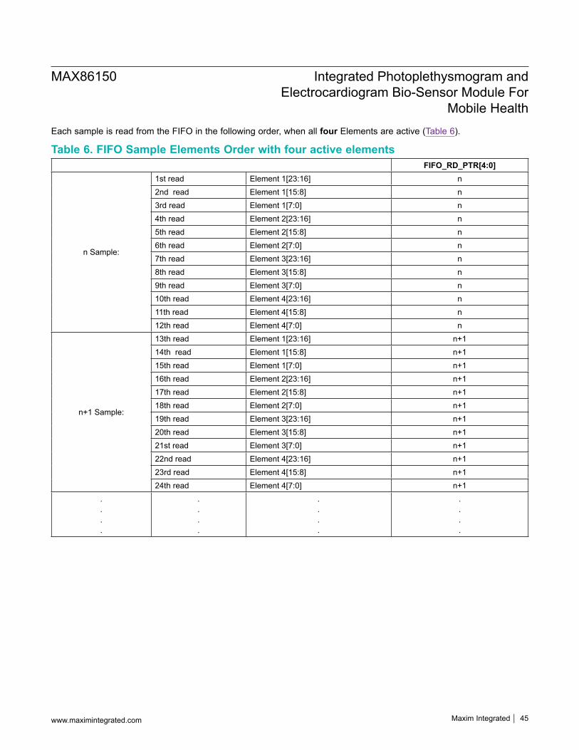
Each sample is read from the FIFO in the following order, when all four Elements are active (Table 6).
Table 6. FIFO Sample Elements Order with four active elementsFIFO_RD_PTR[4:0]
n Sample:
1st read Element 1[23:16] n2nd read Element 1[15:8] n3rd read Element 1[7:0] n4th read Element 2[23:16] n5th read Element 2[15:8] n6th read Element 2[7:0] n7th read Element 3[23:16] n8th read Element 3[15:8] n9th read Element 3[7:0] n10th read Element 4[23:16] n11th read Element 4[15:8] n12th read Element 4[7:0] n
n+1 Sample:
13th read Element 1[23:16] n+114th read Element 1[15:8] n+115th read Element 1[7:0] n+116th read Element 2[23:16] n+117th read Element 2[15:8] n+118th read Element 2[7:0] n+119th read Element 3[23:16] n+120th read Element 3[15:8] n+121st read Element 3[7:0] n+122nd read Element 4[23:16] n+123rd read Element 4[15:8] n+124th read Element 4[7:0] n+1
.
.
.
.
.
.
.
.
.
.
.
.
.
.
.
.
www.maximintegrated.com Maxim Integrated 45
MAX86150 Integrated Photoplethysmogram and Electrocardiogram Bio-Sensor Module For
Mobile Health
Each sample is read from the FIFO in the following order, when any two Elements are active (Table 7).
Enable Push on FIFO FULL, FIFO_ROLLS_ON_FULL: This bit determines whether samples get pushed on to the FIFO when it is full. If push is enabled when FIFO is full, old samples are lost. Otherwise, new samples are lost.Overflow counter, OVF_COUNTER[4:0]: When the FIFO is full, samples are lost. OVF_COUNTER counts the number of samples lost. It saturates at 0x1F. When a complete sample is popped from the FIFO (when the read pointer advances), and OVF_COUNTER is reset to zero.FIFO Almost Full Counter, FIFO_AFULL_COUNT[3:0]: This determines the amount of space available in the FIFO, to declare that it is almost full.FIFO Almost Full status, and Interrupt Enable, A_FULL and MSK_A_FULL: When the FIFO is almost full, the almost full interrupt is asserted if it is enabled by the MSK_A_FULL bit. This prompts the AP to read some samples before the FIFO gets full. A_FULL bit is cleared when the status register is read.The AP reads the FIFO_WR_PTR and FIFO_RD_PTR to calculate the number of samples available in the FIFO, and read as many samples as it needs up to a maximum of available samples. The AP can then choose to write the new read pointer to the FIFO_RD_PTR register. If necessary to retry, the AP updates the FIF_RD_PTR register with appropriate value.
Example: Following is an example of the pseudo code:First transaction: Get the FIFO_WR_PTR and FIFO_RD_PTR:
AP evaluates the number of samples to be read from the FIFO:
If OVF_COUNTER is zero,NUM_AVAILABLE_SAMPLES = FIFO_WR_PTR – FIFO_RD_PTR(Note: pointer wrap around should be taken into account)If OVF_COUNTER is non-zero some samples are lost, andNUM_AVAILABLE_SAMPLES = 32NUM_SAMPLES_TO_READ = < less than or equal to NUM_AVAILABLE_SAMPLES >
Table 7. FIFO Sample Elements Order with two active elementsFIFO_RD_PTR[4:0]
n Sample:
1st read Element 1[23:16] n2nd read Element 1[15:8] n3rd read Element 1[7:0] n4th read Element 2[23:16] n5th read Element 2[15:8] n6th read Element 2[7:0] n
n+1 Sample:
7th read Element 1[23:16] n+18th read Element 1[15:8] n+19th read Element 1[7:0] n+110th read Element 2[23:16] n+111th read Element 2[15:8] n+112th read Element 2[7:0] n+1
.
.
.
.
.
.
.
.
.
.
.
.
.
.
.
.
www.maximintegrated.com Maxim Integrated 46
MAX86150 Integrated Photoplethysmogram and Electrocardiogram Bio-Sensor Module For
Mobile Health
Next transaction: Read NUM_SAMPLES_TO_READ samples from the FIFO:
Next transaction: Write to FIFO_RD_PTR register. If the pervious transaction was successful, FIFO_RD_PTR points to the next sample in the FIFO, and this transaction is not necessary. Otherwise, the AP updates the FIFO_RD_PTR appropriately to New_FIFO_RD_PTR, so that the samples are reread.
START;Send device address + write modeSend address of FIFO_RD_PTR;Write New_FIFO_RD_PTR;STOP;
FIFO FlushThe FIFO gets flushed if FIFO_EN = 1, and if any of the following conditions are met:
I2C write to any of the PPG Configuration registers I2C write to any of the ECG Configuration registers I2C write to any of the FIFO Data Control registers At the rising edge of FIFO_EN Enter and exit PROX mode
When the FIFO gets flushed, FIFO_WR_PTR and FIFO_RD_PTR are reset to zero, and the contents of the FIFO are lost.If FIFO contents should not be lost, set FIFO_EN = 0, before writing to any of the registers listed above.Note: FIFO_EN bit is in the System Control register. Data is pushed to the FIFO, when FIFO_EN = 1. When FIFO_EN = 0, push to FIFO is disabled, but it holds the status of the FIFO (FIFO pointers and the actual data).
FIFO OrganizationFigure 9 shows how the samples are organized in the FIFO when all four elements in a sample are active.Figure 10 shows how the samples are organized in the FIFO when only two elements in a sample are active.
www.maximintegrated.com Maxim Integrated 47
MAX86150 Integrated Photoplethysmogram and Electrocardiogram Bio-Sensor Module For
Mobile Health
Figure 9. Example of FIFO Organization with Four Active Elements
www.maximintegrated.com Maxim Integrated 48
MAX86150 Integrated Photoplethysmogram and Electrocardiogram Bio-Sensor Module For
PART TEMP RANGE PIN-PACKAGEMAX86150EFF+T -40°C to +85°C 22-Lead OESIP
+Denotes a lead(Pb)-free/RoHS-compliant package. T = Tape-and-reel.
0.1μF
3.3V
MAX86150
NC1
NC
ECG_N
ECG_P
INTB
SDA
GND _DIG
GND _ANA
VREF
C1_N
C1_P
SCL
PGND
VLED
2
3
4
5
6
7
8
9
10
21
20
19
18
17
16
15
14
13
12
22
110.1μF 4.7μF
1.8V
1μF
1μF
NC
VDD _DIG
VDD _ANA
NC
NC
NCNC 10μF
NC50kΩ
50kΩ
10pF
10pF
Note 1: The RC Circuits added to the ECG_P and ECG_N are for Current Limiting and RF/EMI filtering purposes.It’s value are system dependent.
Note 2: The value of I 2C and INTB pull up resistors should be based on the system design .Note 3: We suggest dedicated 1.8V for VDD _ANA whenever possible, otherwise VDD_ANA is suggested to be
isolated from other supplies, such as VDD_DIG.Note 4: Use common design practice to isolate noise coupling between GND planes .Note 5: VDDIO is the system I/O voltage supply.
Note 1
VDDIO note 5
1kΩ
note
2
1kΩ
note
2
1kΩ
note
2
HOST PROCESSOR
0.1μF 4.7μF
D1.8V
1.8VD1.8V
PGND GND _DIGGND_ANA
0 0Note 4
Note 3
www.maximintegrated.com Maxim Integrated 50
MAX86150 Integrated Photoplethysmogram and Electrocardiogram Bio-Sensor Module For
Mobile Health
Ordering Information
Typical Application Circuit
REVISIONNUMBER
REVISIONDATE
DESCRIPTIONPAGES
CHANGED
0 12/15 Initial release —1 11/16 General updates and typo corrections 1–47
Maxim Integrated cannot assume responsibility for use of any circuitry other than circuitry entirely embodied in a Maxim Integrated product. No circuit patent licenses are implied. Maxim Integrated reserves the right to change the circuitry and specifications without notice at any time. The parametric values (min and max limits) shown in the Electrical Characteristics table are guaranteed. Other parametric values quoted in this data sheet are provided for guidance.
MAX86150 Integrated Photoplethysmogram and Electrocardiogram Bio-Sensor Module For
Mobile Health
Revision History
For pricing, delivery, and ordering information, please contact Maxim Direct at 1-888-629-4642, or visit Maxim Integrated’s website at www.maximintegrated.com.