»•M*"«N»)»*«MMMfti ««MMW^W-: i <w unrw lim '%' ***,y*&.*'» rf'Ä&tt-'i.W '•'/; < *S^ •^•'•w**WHi.r: Security Glastfiinciition ÖOCÜMisNT CONTROL DATA • R-^U GTK tSylvania Tue. 3. RnF'ORI rtTLI Infrared Photocathode ,> I! (» ft (»ö H t » h "; Ll HI T V C l. A » 011' I C A T IU N i/MCLASSIFIEP ^ 4 t>IICfUI*TIVK NOTBI (Typ* of re|wM «ml tnptoiln daltu ,, „« ;f,To Annual Report "ay 1 Iv/l ~ April JU i l .'/-i Nt >. AUTHORS fLul nMn«i nMitl*ms< iniilalj H. Sonnenberg iAL Xj April 3Ü, 197; [,/: CO'-'Tf.'CT Or. GRANT NO. NOOO.U-70-C-0079 h. PROJKCT NO. 7«. TOTAL NO. OP f'ACll",» 20 la. QNiaiNATOM 1 ! HKi'ofiT NUMftllW None ;b, Nf OP R«P» 14 tb, STHM in;POMT NOW fXny o(hif numb»« l/i«( m«y b* *<i«'<; r i*d CiJ,» laport) None 10. AVAtUAitUITV/UMITATtON MOTICW Unliiiii tod n. sr-oNi.r>niHO MILITAHY ACTIVITY Advanced Research Piojectc Agency II. AB»TRACT 7.^- The , im0lint 0 f cs-0 low-V7ork--func.tion-suri:ace material required to cmtimiKe the phOtpraspöttM of InAsITVP. .depend» upon the wavelength at which the rMponsa is to be piaÄIVea 1 ?' It is shown that the optimum thickness increaae« exponentially with wavelength. The effect of thick Cs-0 layers on photocraission from GaAs and Ir^oJ^TP/^cathodor, is experimentally investigated. Simple empirical relafcolfhiis between the yield and thickness and between the escape probability and thickness are derived. NATIONAL TECHNICAL INFORMATION SERVICE Spring«»«, V«. 32ISI I ,., jw*.irr»i.--. r** DD .^«1473 UNCLASSIFIED 18 Security Clos;sifk-ation \
Transcript
»•M*"«N»)»*«MMMfti ««MMW^W-: i <w unrw lim '%'■***,y*&.*'» rf'Ä&tt-'i.W '•'/;■< *S^ •^•'•w**WHi.r: Security Glastfiinciition ÖOCÜMisNT CONTROL DATA • R-^U
GTK tSylvania Tue.
3. RnF'ORI rtTLI
Infrared Photocathode
,> I! (» ft (»ö H t » h "; Ll HI T V C l. A » 011' I C A T IU N
7.^-The ,im0lint 0f cs-0 low-V7ork--func.tion-suri:ace material required to
cmtimiKe the phOtpraspöttM of InAsITVP. .depend» upon the wavelength at which the rMponsa is to be piaÄIVea1?' It is shown that the optimum thickness increaae« exponentially with wavelength.
The effect of thick Cs-0 layers on photocraission from GaAs and Ir^oJ^TP/^cathodor, is experimentally investigated. Simple empirical relafcolfhiis between the yield and thickness and between the escape
probability and thickness are derived.
NATIONAL TECHNICAL INFORMATION SERVICE
Spring«»«, V«. 32ISI
I ,., jw*.irr»i.--. r**
DD .^«1473 UNCLASSIFIED
18
Security Clos;sifk-ation
\
BEST AVAILABLE COPY
UNCLASSiirro. Security Classlftcation
1 ORIOINATING ACTIVITY: Enter the name and Bd&MIl of ,ho ^ntractor, subcontractor, erantre, D^^t.r.enl of D- ?ea"P uctivity or other oreani--.Uion (corpotvte m.thor) UMtKg the rcpott. 5« REPORT SKCURITY CLAPSII-TCATION: Enter the over-
ance with appropriate security regiüations. 2b CROUP: Automatic downGradinR tl specified in DoD Di-
• • Vonri in nnd Ar"u-d Farces Imiustrii.I Manual, hmtr rect.ve 52^;J« "nd ^^'-^^ ap.,Ucable, show that optional •'^S SSS.^*« »A 3 S- Coup 4 as author-
i Rl-PORT TITLE: Ent'.-r the complete repoit tit'.e in ßU • . > M m VMmm in •til cases should be unclassifiod.
cap.tal le to« ^ l ^^o U
tn"se^cted wilhout classifica- ^"ÄSlÄÄioj in all capita.« in parenthests itnincdialely lollowirg the title. 4 DESCRlPVl'E NOTES: If appropriate, enter the type Of
covered. 5 AUTHOR(S): Enter the namc(E) of ^'''^^.^.f ^i."^11
IL^S^lTis^^^^^« requ.ement.
««BAcn« riATr- Fnter the date of the report as day, iJfSS "r month";f/ U more than one date appears on tho rcp.-.l, use dale of publication. 7a. TOTAL NUMBER OF PAGES: The ,o.a. paite count should follow normal paKinaUon procedures, ..e., enter nun-hor of pOK»* containin,- inlormat.o^ 7b. NUMIiFK OF REFERENCES Enter the tote, number of referenceu tiled in the repoit. „ t^MmtACT OR GRANT NUMBER: U appropriate, enter K appi'^U numb^f the contract or grant under which .Me ri'poit was written. ofc a,, fc ßrf PROJECT NUMBER: Enter the appropriate
<>a. OR^lNATOR'S «^^^S^i.rrid^iücd
be unitiueto tnio report.
"r 1 "/.« *pun.so,;, al»o enter thi» numbeKs). ,0. AVAILABtL.TY/L.M.TAT10N NOT.CES: ^-V - t
Vationr. on turtlier dissemination ol the report, otner
imposed by security classification, using standard statements such as:
(1)
(2)
(3)
(4)
(8)
'Qualified requesters may obtain copies of this report from DDC" "ForeiKn announcement and dissemination of this report by DDC is not authorized. "U. 3. Governnienl agencies may obtain copies of .his report directly to« DDC. Other quahf.ed DDC uaeis shall rcqUMt through
"U S militurv agencies may obtain copies of this rirTdTrec.iyNro,. DDC Oth« qualified users shall request through
"All distribution of this report is controlled, ified DDC users shall request Inrough
Qu.-.l-
If the rtport has been furnished to the Office of J"*"""1
Series! Department of Commerce for sale to the public, md,- cal^ this fact and enter the price, if known. U. SUPPLEMENTARY NOTES: Use for additional explana-
tory notes. 1? SPOORING MILITARY ACTIVITY; Kntcr the name of It d.?ar montal project office or laboratory «i~^ ('^ .ng (or) the research and development. Include address. 11 ABSTRACT: Enter an abstract giving a brief and factual
po^ UaddUiLal space is required, a continuation sheet shall
be attached. It U hiuhly desirable that the abstract of cUssified reports
be unclasr n , • Each paragraph of the abstract shal end with
^n rndication of the military --"%'?*^ws" IcTo'W formation in the paragraph, represented a? (TS). (S). (C). ( There is no limitation en the lengf.. of the abstract. How-
ever, the suggested length is from 150 to 22b words. 14 KFY WORDS: Key words ore technically meaningful terns or short phTes'tha, characte.i.e a »P»" "< ««*.^ aS
mdex entries for cataloging tho report. Ley '»•^««•IW» sei cted so that no security classif.c »tion is required. Ide""; neVs' such as ecuipment UK-de! der.^ation, ti.u'o name, military nroiccl code name, geogruphu location, may be user; as key Cds but wil" be ortowedbv an indication of technical con- SSTTM •Wl^.nt of linkt, rules, and weight, is optional.
UNCLASSIFIED
"Security Clnssification
INFRARED rilüTUCATUODE
AlWUAI. TECHNICAL REfORT
iH ARl'A Order Nambcr:
Trogram Code Nmibet:
Contractor:
Effective Date:
Expiration Date:
Contract Amount:
Contract Number:
Principal Investigator
Tclephone:
Scientific Officer:
1806
00014
GTE Sylvsnia Inc.
1 November 1969
30 April 1972
$178,686
NOOO] 4-70-00079
Dr. U. Sonnenberg
(415) 966-3472
Dr. Robert E. Behringer
*. view, ana »nolu.10«. f f ^^.^n^Ä^f.lc^oUci«.
U. S. Government.
Prepared by
Sponsored by
Advanced Research Projects Agency
ARPA Order No. 1806
Approved by
D D C n|E(2[EIEQE
MAY 4 1912
fEiSEinrE c -
£ gj^- -ifmJim .1™^;! ' ... Sonnenbcrg Electro-Optics Research and Development Department
H. L. H. Oatcrink', Manager Electro-Optics Research and Development Department
% TECFIJICAL REP0B2 SUMMARY
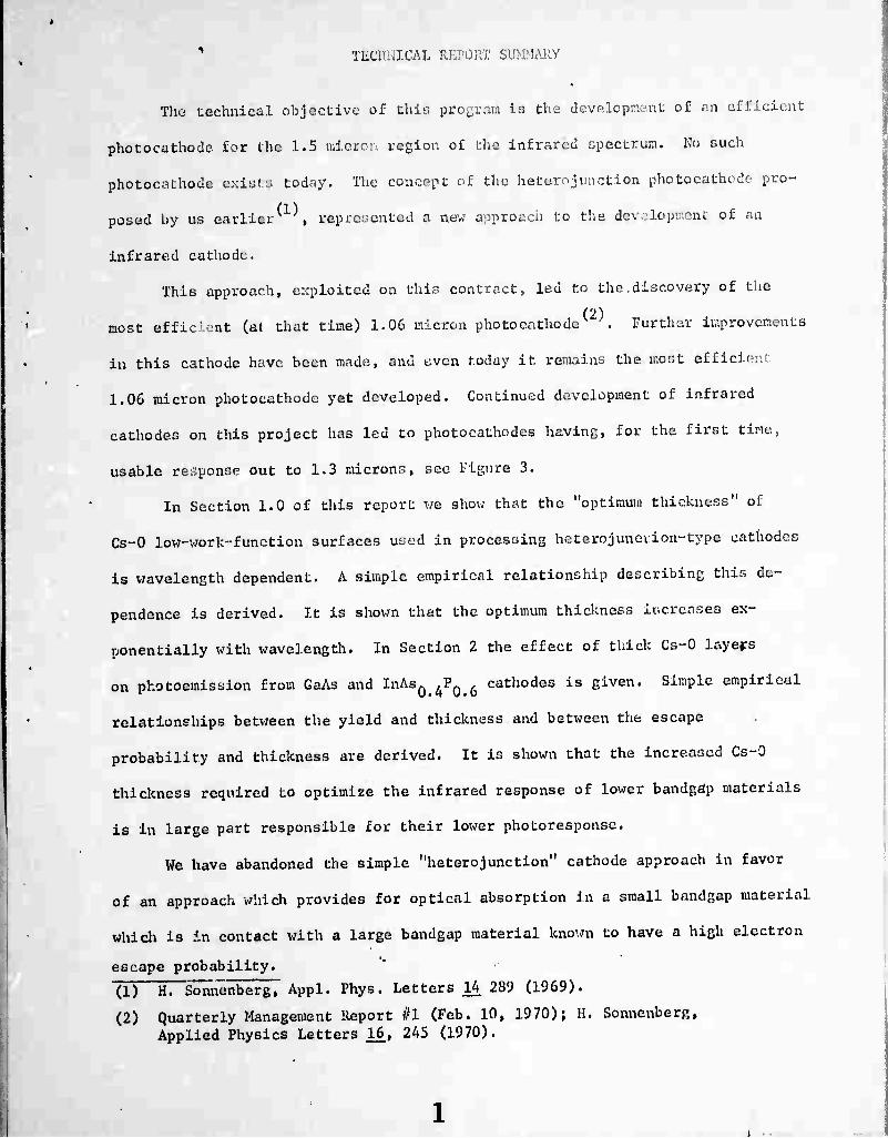
The technical objective of thio program is the developoant of an efficient
photocathode for tlie 1.5 micron region of the infrared spectrum. No such
photocathode exists today. The concept of the hetcrojunction photocathode pro-
posed by us earlier , represented a new approach to the development of an
infrared cathode.
This approach, exploited on this contracts led to the.discovery of the
(2) most efficient (at that time) 1.06 micron photocathodev '. Further improvements
in this cathode have been made, and even today it remains the most efficient
1.06 micron photocathode yet developed. Continued development of infrared
cathodes on this project has led to photocathodes having, for the first time,
usable response out to 1.3 microns, see Figure 3.
In Section 1.0 of this report we show that the "optimum thickness" of
Cs-0 low-work-function surfaces used in processing heterojunction-type cathodes
is wavelength dependent. A simple empirical relationship describing this de-
pendence is derived. It is shown that the optimum thickness increases ex-
ponentially with wavelength. In Section 2 the effect of thick Cs-0 layeirs
on photoemission from GaAs and InAs0 i?Q - cathodes is given. Simple empirical
relationships between the yield and thickness and between the escape
probability and thickness are derived. It is shown that the increased Cs-0
thickness required to optimize the infrared response of lower bandgap materials
is in large part responsible for their lower photoresponse.
We have abandoned the simple "heterojunction" cathode approach in favor
of an approach which provides for optical absorption in a small bandgap material
which is in contact with a large bandgap material known to have a high electron
the thickn.^ dcrencleacc oi thu yxcld frou i^^^I'^.-at: 0.6^ «idJOlM (upper
curve) and 0.7 «ictOttt (lover curve). Tbe pelntS on the curve, arc the actual
data points, and the solid line repre.ents oquatioa (2) with r^ - 0.062 and
| . 0.6 for tU upper curvc.aud no - 0.0335 and % - 0.5 for the lower curve.
If, as in reference 1, we M»Utt» that the »ticking coefficient of
C on InAsA /Vn t ard on GaAs doe. not chanye sianificant.y with ccvera^P^ s ü.H U«o then the Cs-0 low-work-function 9VXi*m in an infrared-optiiui^d InAöü>/(P0t6
cathode is approximately 2.3 mnnolayers of Co thxeker than tUat of optimised
Ga.Vs. From equation 2 , with ü - 0.65 monolayer., we find that an additional
2.3 monolayers of Cs would reduce the infrared photoresponse of GaAs by a
factor of about 4. We do not luve sufficie..:-. data on 1^Q^0,G ^ allow^ uc;
to determine its attenuation length near threshold, however from Figure 7, we
' expect that it will be smaller than 0.65 monolayers. Consequently alone on
the basis of the increased thickness required to optimise the infrared response
of InAs ,Pn •. we would expect the threshold response of IHA^^PQ^ to be O.'f O.b ^j
lower than that of GaAs by a factor of 5 or more .
•v
14
Figure 7 '0.^0.6 at thlekftasi d»?cu<Umc« of the guaiittmi efJ.iciencv r\ ol XnA;j(
6300R (upper curve.) and 700ÜA (low.rr CUI-VL;) . The points represent the experimental data and the solid curves are plots .
%Oi the equations n - 0.062(1 - o"0-C/t.) md r, - 0.0335(1 - JT0'"*)
for tlie upper and lower curves rcKpcclively•
, I 2
THICKNESS (M0N0LAYERS Cs)
REFERENCES
1.
2.
3.
5.
6.
11. Sonnenberg, Appl. Phy«. Lett .19, 431 (1971).
A monoiayer of Cs is defined here a. the amount of Ci required to
optimize tV.e photore.ponse at 6323^ with Ol only
We assume that the Cs nad 02 sticking coefficients äo not change
significantly with coverage.
The fact that T is greater than 1 shows that .ome 02 is required to
optimize the photoresponsc at all wavelength., including the ultra
violet range.
Note that the efficiency a. 1.3 microns is almost 0.02%. Further
improvement with better InAs^P^ material can be expected.
If we make the same assumptions about the Cs-0 surface that were made
in reference 1. we find that the low-work-function surface consist.
of approximately 1 monoiayer of Cs and 1.7 monolayers of C.^O.
L. U. James and J. J. Uebbing. Appl- «**•• Liters 16. 370 (1970).
R. L. Bell, L. W. Jame., G. A. Antypas, J. Edgecumbe, and R. L. Moon,
Appl. Phys. Letters 19, 513 (1971).
9. The ratio of Cs to 02 remains constant.
L. W. James and J. L. Holl Phys. Rev. 183. 7A0 (1969).
High escape probabilities such as this were achieved with <110> GaAs
surfaces. Our best yield curves obtained in this material are comparable
to those obtained on <111B> GaAs by.L. W. James, G. A. Antypas,
j. Edgecumbe, R. L. Moon, and R. L. Bell, J. of Appl. Phys. 42, 4976
(1971). Our yield is slightly better than theirs above 1.65 eV but
slightly lower than the.rs below about 1.6 eV. The decreased yield in^ ^
the infrared Is probably due to the low doping of our material (1 x 10 cm ),
L. W. James, J. L. Moll, and W. E. Spicer Symposium on GaAs, 230. (1968).
7.
8.
10.
11.
12.
16
13. The fact that the BAtting o£ the Cr^ channel at the point of equJ llbriura
(Ca loss « CH gain) remains efjsentially the. same at all exposure 1evels,
seems to confirm that the assumption is valid.
14. Since the thickness of the low-work-function surface has such a profound
effect on pbotoemission, it is not surprising that a g^at deal of
progress in the processing of infrared cathodes has recencly been made.