RF and Protect ion Devices
BGS22WL10
Appl icat ion Note AN302 Revision: Rev. 1.0
2012-11-29
Performance of DPDT (Dual -Pole / Double-Throw) RF MOS switch
Broadband Di f ferent ia l LTE, WCDMA, CDMA, UMTS Mobi le Diversi ty Appl icat ions
Edition 2013-06-26
Published by Infineon Technologies AG 81726 Munich, Germany
© 2013 Infineon Technologies AG All Rights Reserved.
LEGAL DISCLAIMER
THE INFORMATION GIVEN IN THIS APPLICATION NOTE IS GIVEN AS A HINT FOR THE IMPLEMENTATION OF THE INFINEON TECHNOLOGIES COMPONENT ONLY AND SHALL NOT BE REGARDED AS ANY DESCRIPTION OR WARRANTY OF A CERTAIN FUNCTIONALITY, CONDITION OR QUALITY OF THE INFINEON TECHNOLOGIES COMPONENT. THE RECIPIENT OF THIS APPLICATION NOTE MUST VERIFY ANY FUNCTION DESCRIBED HEREIN IN THE REAL APPLICATION. INFINEON TECHNOLOGIES HEREBY DISCLAIMS ANY AND ALL WARRANTIES AND LIABILITIES OF ANY KIND (INCLUDING WITHOUT LIMITATION WARRANTIES OF NON-INFRINGEMENT OF INTELLECTUAL PROPERTY RIGHTS OF ANY THIRD PARTY) WITH RESPECT TO ANY AND ALL INFORMATION GIVEN IN THIS APPLICATION NOTE.
Information
For further information on technology, delivery terms and conditions and prices, please contact the nearest Infineon Technologies Office (www.infineon.com).
Warnings
Due to technical requirements, components may contain dangerous substances. For information on the types in question, please contact the nearest Infineon Technologies Office.
Infineon Technologies components may be used in life-support devices or systems only with the express written approval of Infineon Technologies, if a failure of such components can reasonably be expected to cause the failure of that life-support device or system or to affect the safety or effectiveness of that device or system. Life support devices or systems are intended to be implanted in the human body or to support and/or maintain and sustain and/or protect human life. If they fail, it is reasonable to assume that the health of the user or other persons may be endangered.
BGS22WL10 Broadband Diffential Diversity Applications
Application Note AN302, Rev. 1.0 2012-11-29 3 / 27
Application Note AN302
Revision History: 2012-11-29
Previous Revision: prev. Rev. x.x
Page Subjects (major changes since last revision)
Trademarks of Infineon Technologies AG
A GOLD™, BlueMoon™, COMNEON™, CONVERGATE™, COSIC™, C166™, CROSSAVE™, CanPAK™, CIPOS™, CoolMOS™, CoolSET™, CONVERPATH™, CORECONTROL™, DAVE™, DUALFALC™, DUSLIC™, EasyPIM™, EconoBRIDGE™, EconoDUAL™, EconoPACK™, EconoPIM™, E GOLD™, EiceDRIVER™, EUPEC™, ELIC™, EPIC™, FALC™, FCOS™, FLEXISLIC™, GEMINAX™, GOLDMOS™, HITFET™, HybridPACK™, INCA™, ISAC™, ISOFACE™, IsoPACK™, IWORX™, M GOLD™, MIPAQ™, ModSTACK™, MUSLIC™, my d™, NovalithIC™, OCTALFALC™, OCTAT™, OmniTune™, OmniVia™, OptiMOS™, OPTIVERSE™, ORIGA™, PROFET™, PRO SIL™, PrimePACK™, QUADFALC™, RASIC™, ReverSave™, SatRIC™, SCEPTRE™, SCOUT™, S GOLD™, SensoNor™, SEROCCO™, SICOFI™, SIEGET™, SINDRION™, SLIC™, SMARTi™, SmartLEWIS™, SMINT™, SOCRATES™, TEMPFET™, thinQ!™, TrueNTRY™, TriCore™, TRENCHSTOP™, VINAX™, VINETIC™, VIONTIC™, WildPass™, X GOLD™, XMM™, X PMU™, XPOSYS™, XWAY™.
Other Trademarks
AMBA™, ARM™, MULTI ICE™, PRIMECELL™, REALVIEW™, THUMB™ of ARM Limited, UK. AUTOSAR™ is licensed by AUTOSAR development partnership. Bluetooth™ of Bluetooth SIG Inc. CAT iq™ of DECT Forum. COLOSSUS™, FirstGPS™ of Trimble Navigation Ltd. EMV™ of EMVCo, LLC (Visa Holdings Inc.). EPCOS™ of Epcos AG. FLEXGO™ of Microsoft Corporation. FlexRay™ is licensed by FlexRay Consortium. HYPERTERMINAL™ of Hilgraeve Incorporated. IEC™ of Commission Electrotechnique Internationale. IrDA™ of Infrared Data Association Corporation. ISO™ of INTERNATIONAL ORGANIZATION FOR STANDARDIZATION. MATLAB™ of MathWorks, Inc. MAXIM™ of Maxim Integrated Products, Inc. MICROTEC™, NUCLEUS™ of Mentor Graphics Corporation. Mifare™ of NXP. MIPI™ of MIPI Alliance, Inc. MIPS™ of MIPS Technologies, Inc., USA. muRata™ of MURATA MANUFACTURING CO. OmniVision™ of OmniVision Technologies, Inc. Openwave™ Openwave Systems Inc. RED HAT™ Red Hat, Inc. RFMD™ RF Micro Devices, Inc. SIRIUS™ of Sirius Sattelite Radio Inc. SOLARIS™ of Sun Microsystems, Inc. SPANSION™ of Spansion LLC Ltd. Symbian™ of Symbian Software Limited. TAIYO YUDEN™ of Taiyo Yuden Co. TEAKLITE™ of CEVA, Inc. TEKTRONIX™ of Tektronix Inc. TOKO™ of TOKO KABUSHIKI KAISHA TA. UNIX™ of X/Open Company Limited. VERILOG™, PALLADIUM™ of Cadence Design Systems, Inc. VLYNQ™ of Texas Instruments Incorporated. VXWORKS™, WIND RIVER™ of WIND RIVER SYSTEMS, INC. ZETEX™ of Diodes Zetex Limited.
Last Trademarks Update 2009 10 19
BGS22WL10 Broadband Diffential Diversity Applications
List of Content, Figures and Tables
Application Note AN302, Rev. 1.0 2012-11-29 4 / 27
Table of Content
1 Introduction ........................................................................................................................................ 6
2 Features .............................................................................................................................................. 7 2.1 Main Features ...................................................................................................................................... 7 2.2 Functional Diagram .............................................................................................................................. 7 2.3 Signal Description ................................................................................................................................ 8
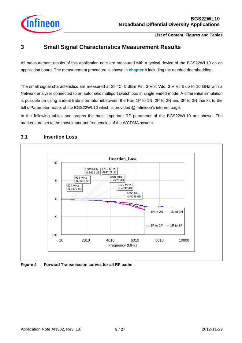
3 Small Signal Characteristics Measurement Results ...................................................................... 9 3.1 Insertion Loss ....................................................................................................................................... 9 3.2 Return loss ......................................................................................................................................... 10 3.3 Isolation of inactive paths ................................................................................................................... 12
4 Switching time .................................................................................................................................. 14 4.1 Measurement Specifications .............................................................................................................. 14 4.2 Measurement Setup ........................................................................................................................... 15 4.3 Measurement results .......................................................................................................................... 16
5 Intermodulation ................................................................................................................................ 17 5.1 Test conditions ................................................................................................................................... 17 5.2 Measurement Setup ........................................................................................................................... 18 5.3 Measurement results .......................................................................................................................... 19
6 Harmonic Generation ....................................................................................................................... 20 6.1 Measurement setup ........................................................................................................................... 20 6.2 Measurement results .......................................................................................................................... 21 6.2.1 Low Band (824 MHz) ......................................................................................................................... 21 6.2.2 High Band (1800 MHz) ....................................................................................................................... 22
7 Power Compression Measurements .............................................................................................. 23
8 Application Board and Measurement desciption ......................................................................... 24 8.1 Application board................................................................................................................................ 24 8.2 Measurement description and deembedding ..................................................................................... 25
Author 26
BGS22WL10 Broadband Diffential Diversity Applications
List of Content, Figures and Tables
Application Note AN302, Rev. 1.0 2012-11-29 5 / 27
List of Figures
Figure 1 Differential Band select Switching application ..................................................................................... 6 Figure 2 Functional Diagram .............................................................................................................................. 7 Figure 3 Pin configuration of BGS22WL10 ........................................................................................................ 8 Figure 4 Forward Transmission curves for all RF paths .................................................................................... 9 Figure 5 Return loss for active port 2 (2P/2N) .................................................................................................. 10 Figure 6 Return loss for active port 3 (3P/3N) .................................................................................................. 11 Figure 7 Isolation of Port 3 (3P/3N) by active Port 2 (2P/2N) .......................................................................... 12 Figure 8 Isolation of Port 2 (2P/2N) by active Port 3 (3P/3N) .......................................................................... 13 Figure 9 Switching Time ................................................................................................................................... 14 Figure 10 Rise/Fall Time .................................................................................................................................... 14 Figure 11 Switching Time Measurement Setup ................................................................................................. 15 Figure 12 Switching Time of BGS22WL10 ......................................................................................................... 16 Figure 13 Block diagram of RF Switch intermodulation ..................................................................................... 17 Figure 14 Test set-up for IMD Measurements .................................................................................................... 18 Figure 15 Set-up for harmonics measurement ................................................................................................... 20 Figure 16 2
nd harmonic at fc=824 MHz ............................................................................................................... 21
Figure 17 3rd
harmonic at fc=824 MHz ................................................................................................................ 21 Figure 18 2
nd harmonic at fc=1800 MHz ............................................................................................................. 22
Figure 19 3rd
harmonic at fc=1800 MHz .............................................................................................................. 22 Figure 20 Power Compression Measurement Results at fc=824 MHz ............................................................... 23 Figure 21 BGS22WL10 application board .......................................................................................................... 24 Figure 22 Layout of the application board and deembedding kit ....................................................................... 24 Figure 23 PCB layer information ........................................................................................................................ 24 Figure 24 SMA connector for deembedding procedure ..................................................................................... 25
List of Tables
Table 1 Device desciption ................................................................................................................................. 6 Table 2 Pin Description (top view) .................................................................................................................... 8 Table 3 Truth table ............................................................................................................................................ 8 Table 4 Insertion Loss of throw between port1 (1P/1N) and port2 (2P/2N) .................................................... 10 Table 5 Insertion Loss of throw between port1 (1P/1N) and port3 (3P/3N) .................................................... 10 Table 6 Return loss of active ports .................................................................................................................. 11 Table 7 Isolation of Port3 (3P/3N) bby active port 2 (2P/2N) .......................................................................... 12 Table 8 Isolation of Port2 (2P/2N) bby active port 3 (3P/3N) .......................................................................... 13 Table 9 Switching time measurement results of BGS22WL10 ....................................................................... 16 Table 10 Test conditions and specifications of IMD measurements ................................................................. 17 Table 11 IMD products of Band I ...................................................................................................................... 19 Table 12 IMD products of Band V ..................................................................................................................... 19
BGS22WL10 Broadband Diffential Diversity Applications
List of Content, Figures and Tables
Application Note AN302, Rev. 1.0 2012-11-29 6 / 27
1 Introduction
The BGS22WL10 RF MOS switch is specifically designed for differential diversity applications (e.g. Figure 1) in
low bands up to 3 GHz like 3G WCDMA diversity, CDMA diversity, UMTS diversity or LTE diversity RF frontend
system solutions. Therefore, the Insertion loss of the BGS22WL10 below 2 GHz is closed to 0.35 dB, upto 3
GHz the IL is in the range of 0.45 dB and the port to port Isolation is more than 26 dB. A typical application is to
combine two Rx paths in a mobile cellular device after the Rx filters or duplexers into one input to the tranceiver
IC. The IC can also be used for a wide variety of applications switching balanced signals in a frequency range of
0.1 - 3 GHz.
B3L
B1&B8
B7L
B20L
DP
DT
DP
DT
UMTS/LTE
TransceiverIC
Div
ers
ity In
pu
ts
B1 High Band
Low Band
Diversity Switch
Diversity
Antenna
B20L
B3L
Figure 1 Differential Band select Switching application
Unlike GaAs technology, external DC blocking capacitors at the RF Ports are only required if DC voltage is
applied externally. The BGS22WL10 RF Switch is manufactured in Infineon’s patented MOS technology,
offering the performance of GaAs with the economy and integration of conventional CMOS including the
inherent higher ESD robustness. This DPDT (Dual-Pole / Double Throw) RF MOS switch which combines two
differential signals into one differential output or splits one differential signal into two separate differential lines.
The parallel paths of the
switch are controlled simultaneously through the same signals. The switch is designed to operate in battery
powered applications with a supply voltage range of 2.4 - 3.6 V while the current consumption is below 300 μA.
The highly symmetric design ensures best phase- and amplitude accuracy.
The RF switch is packaged in a standard RoHS compliant TSLP-10-1 package with a small outline of only 1.55
x 1.15 mm².
Table 1 Device desciption
Product Name Product Type Package Marking
BGS22WL10 DPDT RF Switch TSLP-10-1 W2
BGS22WL10 Broadband Diffential Diversity Applications
List of Content, Figures and Tables
Application Note AN302, Rev. 1.0 2012-11-29 7 / 27
2 Features
2.1 Main Features
DPDT (Dual-Pole / Double-Throw) differential RF switch
All ports fully symmetrical
High ESD robustness
Frequency range: 0.1 - 3 GHz
High signal power up to 30 dBm
Extremely low insertin loss
High port-to-port-isolation
Supply voltage 2.4 - 3.6 V
No decoupling capacitors required if no DC applied on RF lines
Lead and halogen free package (RoHS and WEEE compliant)
Small leadless package TSLP-10-1 with the size of 1.55 x 1.15 mm² and a maximum height of 0.77 mm.
2.2 Functional Diagram
Port 3P
Port 3N
BGS22W2L10
Port 1P
Port 1N
VCTRL
ESD Protection
VDD
Port 2P
Port 2N
DPDT
Figure 2 Functional Diagram
BGS22WL10 Broadband Diffential Diversity Applications
List of Content, Figures and Tables
Application Note AN302, Rev. 1.0 2012-11-29 8 / 27
2.3 Signal Description
Table 2 Pin Description (top view)
Pin NO Name Pin Type Function
1 Port 3P I/O RF port 3P
2 GND GND Ground
3 GND GND Ground
4 Port 2N I/O RF port 2N
5 Port 2P I/O RF port 2P
6 CTRL I Control Pin
7 Port 1P I/O RF port 1P
8 Port 1N I/O RF port 1N
9 VDD Supply Supply voltage
10 CTRL I Control Pin
Figure 3 Pin configuration of BGS22WL10
Table 3 Truth table
Pin No. Control
Port1 to Port2 0
Port1 to Port3 1
BGS22WL10 Broadband Diffential Diversity Applications
List of Content, Figures and Tables
Application Note AN302, Rev. 1.0 2012-11-29 9 / 27
3 Small Signal Characteristics Measurement Results
All measurement results of this application note are measured with a typical device of the BGS22WL10 on an
application board. The measurement procedure is shown in chapter 8 including the needed deembedding.
The small signal characteristics are measured at 25 °C, 0 dBm Pin, 3 Volt Vdd, 3 V Vcrlt up to 10 GHz with a
Network analyzer connected to an automatic multiport switch box in single ended mode. A differential simulation
is possible ba using a ideal trabnsformator inbetween the Port 1P to 1N, 2P to 2N and 3P to 3N thanks to the
full s-Parameter matrix of the BGS22WL10 which is provided @ Infinieon’s internet page.
In the following tables and graphs the most important RF parameter of the BGS22WL10 are shown. The
markers are set to the most important frequencies of the WCDMA system.
3.1 Insertion Loss
10 2010 4010 6010 8010 10000
Frequency (MHz)
Insertion_Loss
-10
-5
0
5
10
824 MHz-0.3479 dB
915 MHz-0.3618 dB
1910 MHz-0.4226 dB
1000 MHz-0.3632 dB
2170 MHz-0.4397 dB
2690 MHz-0.5038 dB
1710 MHz-0.4109 dB
1N to 2N
1P to 2P
1N to 3N
1P to 3P
Figure 4 Forward Transmission curves for all RF paths
BGS22WL10 Broadband Diffential Diversity Applications
List of Content, Figures and Tables
Application Note AN302, Rev. 1.0 2012-11-29 10 / 27
Table 4 Insertion Loss of throw between port1 (1P/1N) and port2 (2P/2N)
Frequency (MHz) 824 915 1000 1710 1910 2170 2690 RF path
1P 2P 0.35 0.36 0.36 0.41 0.42 0.44 0.5
1N 2N 0.34 0.35 0.35 0.41 0.42 0.44 0.52
Table 5 Insertion Loss of throw between port1 (1P/1N) and port3 (3P/3N)
Frequency (MHz) 824 915 1000 1710 1910 2170 2690 RF path
1P 3P 0.34 0.35 0.36 0.41 0.41 0.43 0.5
1N 3N 0.34 0.36 0.36 0.42 0.43 0.44 0.5
3.2 Return loss
10 2010 4010 6010 8010 10000
Frequency (MHz)
Return loss Port1 to Port2 active
-40
-30
-20
-10
0
1N
1P
2N
2P
Figure 5 Return loss for active port 2 (2P/2N)
BGS22WL10 Broadband Diffential Diversity Applications
List of Content, Figures and Tables
Application Note AN302, Rev. 1.0 2012-11-29 11 / 27
10 2010 4010 6010 8010 10000
Frequency (MHz)
Return loss Port1 to Port3 active
-40
-30
-20
-10
0
1N
3P
3N
1P
Figure 6 Return loss for active port 3 (3P/3N)
Table 6 Return loss of active ports
Frequency (MHz) port 824 915 1000 1710 1910 2170 2690
Active Path
Throw port 1 to port 2
1P -29.4 -28.2 -28.8 -29.5 -30.5 -33.3 -29.4
1N -29.8 -28.6 -28.6 -27.6 -28.3 -28.6 -22.4
2P -30.2 -28.9 -29 -32.4 -30.2 -33.1 -26.2
2N -30.7 -30.7 -31.4 -27.1 -27.4 -27.7 -21
Throw port 1 to port 3
1P -29.2 -28.7 -23.2 -24.4 -22.5 -28.9 -25.8
1N -32.7 -37.6 -31.6 -32.4 -26.6 -23.9 -31.5
3P -28.9 -27.7 -27 -25.8 -26 -27.3 -25.8
3N -30.9 -29.8 -29.3 -31 -29.3 -29.5 -27.5
BGS22WL10 Broadband Diffential Diversity Applications
List of Content, Figures and Tables
Application Note AN302, Rev. 1.0 2012-11-29 12 / 27
3.3 Isolation of inactive paths
100 2100 4100 6100 8100 10000
Frequency (MHz)
Isolation_2N_2P_active
-80
-60
-40
-20
0
2690 MHz-25.06 dB
3P to 1P
3N to 1P
3N to 1N
3N to 1N
3P to 2P
3P to 2N
3N to 2P
3N to 2N
Figure 7 Isolation of Port 3 (3P/3N) by active Port 2 (2P/2N)
Table 7 Isolation of Port3 (3P/3N) bby active port 2 (2P/2N)
Port to port isolation
824 915 1000 1710 1910 2170 2690
3P 1P -36 -35 -34.3 -33.1 -29.6 -27.7 -25.1
3N 1P -42.8 -41.8 -41.2 -41.4 -36.6 -34.1 -31.2
3P 1N -45.6 -44.6 -43.6 -40.1 -37.1 -34.1 -31.7
3N 1N -43.3 -42.2 -41.6 -37.3 -35.3 -33.2 -30.6
3P 2P -42.8 -42.2 -41.4 -36.5 -34.3 -31.7 -27.2
3P 2N -48.1 -46.9 -45.6 -39.4 -36.8 -35.6 -31
3N 2P -45.3 -44.4 -43.8 -39.8 -37.1 -34.6 -30.1
3N 2N -50.6 -48.7 -47.5 -38.6 -36.6 -35.9 -31.5
BGS22WL10 Broadband Diffential Diversity Applications
List of Content, Figures and Tables
Application Note AN302, Rev. 1.0 2012-11-29 13 / 27
10 2010 4010 6010 8010 10000
Frequency (MHz)
Isolation_3N_3P_active
-80
-60
-40
-20
0
2P to 1P
2N to 1N
3P to 2P
3P to 2N
3N to 2P
3N to 2N
2P to 1N
2N to 1P
Figure 8 Isolation of Port 2 (2P/2N) by active Port 3 (3P/3N)
Table 8 Isolation of Port2 (2P/2N) bby active port 3 (3P/3N)
Port to port isolation
824 915 1000 1710 1910 2170 2690
2P 1P -36.3 -35.1 -34 -32.9 -29.1 -27.3 -24.2
2N 1P -42.5 -41.3 -41.1 -39.4 -35.6 -34.4 -31.5
2P 1N -45.1 -44.2 -43.6 -40.3 -34.5 -34.2 -31.2
2N 1N -42.5 -41.2 -40.1 -34.8 -33.7 -31.7 -29.5
2P 3P -36 -35 -34 -28.5 -27.9 -26.1 -24.1
2P 3N -48.5 -47 -45.3 -37.9 -35.9 -33.2 -30.2
2N 3P -49 -47.8 -46.5 -37.8 -36 -33.4 -30.3
2N 3N -46 -45.1 -44.3 -37.7 -35.1 -34.1 -30.9
BGS22WL10 Broadband Diffential Diversity Applications
List of Content, Figures and Tables
Application Note AN302, Rev. 1.0 2012-11-29 14 / 27
4 Switching time
4.1 Measurement Specifications
Switching On Time: 50% Trigger signal to 90 % RF Signal
Switching Off Time: 50% Trigger signal to 10% RF Signal
tON
tOFF
VCTRL
RF signal
VCTRL
2
90% RF signal
10% RF signal
Figure 9 Switching Time
Rise time: 10% to 90% RF Signal
Fall time: 90% to 10% RF Signal
tOFF
RF signal
tON
90% RF signal
10% RF signal
Figure 10 Rise/Fall Time
BGS22WL10 Broadband Diffential Diversity Applications
List of Content, Figures and Tables
Application Note AN302, Rev. 1.0 2012-11-29 15 / 27
4.2 Measurement Setup
BGS22WL10
1P 1N
2P
2N
3P
3P
50 Ω
50 Ω
50 Ω
50
Ω
VDD Vctrl
Rf Signal,
1 GHz, +10 dBm
VDD = constant,
3Volt
Pulse Generator Oscilloscope
Signal Generator
3 d
B
1 MΩ input 50 Ω input
Vctrl
RFOUT
RFIN
50 Ω output
1 kHz, 1.8 Volt
50 % Duty Cycle
Figure 11 Switching Time Measurement Setup
The switching Time measurement setup consist of one pulse generator which generates a sqare wave with 50%
duty cycle and an amplitude of 1.8 Volts, an oscilloscope which can detect the 1 GHz signal and the 1 kHz
signal and one Signal generator which is set to an output signal of 1GHz with a power level 10 dBm.
If the oscilloscope can not detect the 1 GHz signal of the RF path, due to small bandwith, it is possible tu use a
cristal oscillator in front of the oscilloscope (such a device detects any RF signal present at input and
commutate that one) that the RF signal can be detected.
BGS22WL10 Broadband Diffential Diversity Applications
List of Content, Figures and Tables
Application Note AN302, Rev. 1.0 2012-11-29 16 / 27
4.3 Measurement results
Figure 12 Switching Time of BGS22WL10
Table 9 Switching time measurement results of BGS22WL10
BGS22WL10 RF rise time (ns) Switching time (ns)
350 607
RF rise time
Switching time
BGS22WL10 Broadband Diffential Diversity Applications
List of Content, Figures and Tables
Application Note AN302, Rev. 1.0 2012-11-29 17 / 27
5 Intermodulation
5.1 Test conditions
Another very important parameter of a RF switch is the large signal capability. One of the possible
intermodulation scenarios is shown in Figure 13.The transmission (Tx) signal from the main antenna is coupled
into the diversity antenna with with high power.This signal (20 dBm) and a received Jammer signal (-15 dBm)
are entering the switch. Thank to the spezified application for the BGS22WL10 inbetween the filters and the
Transceiver, the Tx signal from the main antenna loose until arriving at the switch input moslty 5 to 10 or more
dB, depending of the filter and pcb structure of the RF frontend. The IMD products are measured with a Tx of
20dBm, which is corresponding to the IMD spec of a main antenna diversity switch like Infineons BGSF110GN.
Therefore, the measured IMD products will be extremly better in the spezified application circuit within the filters
and transceiver as showed in the measurement results below.
RF Switch
Diversity
Antenna
Receiver
Coupled Tx
Signal from
main antenna
Jammer
(CW)
IMD
Figure 13 Block diagram of RF Switch intermodulation
Special combinations of TX and Jammer signal are producing intermodulation products 2nd
and 3rd order, which
fall in the RX band and disturb the wanted RX signal.
In Table 10 frequencies for 3 bands and the linearity specifications for an undisturbed communication are given.
Table 10 Test conditions and specifications of IMD measurements
Test Conditions
(Tx = +20dBm, Bl = -15dBm,freq.in MHz,@25°C)
Linearity Specification
Band Tx Freq. Rx Freq. IMD2 Low Jammer 1
IMD3 Jammer 2
IMD2 High Jammer 3
IM2 (dBm)
IIP2 (dBm)
IM3 (dBm)
IIP3 (dBm)
850 836.5 881.5 45 791.5 1718 -105 110 -105 65
1900 1880 1960 80 1800 3840 -105 110 -105 65
2100 1950 2140 190 1760 4090 -105 110 -105 65
BGS22WL10 Broadband Diffential Diversity Applications
List of Content, Figures and Tables
Application Note AN302, Rev. 1.0 2012-11-29 18 / 27
5.2 Measurement Setup
The test setup for the IMD measurements has to provide a very high isolation between RX and TX signals. As
an example the test set-up and the results for the high band are shown (Figure 14 and Table 11).
For the RX / TX separation a professional duplexer with 80 dB isolation is used.
In Table 12 the results for Low band are given.
For each distortion scenario there is a min and a max value given. This variation is caused by a phase shifter
connected between switch and duplexer. In the test set-up the phase shifter represents a no ideal matching of
the switch to 50 Ohm.
Mini Circuits
(ZHL-30W-252 -S+)
Load
Signal Generator
Power Amplifier
Circulator
-20dB
Signal Analyzer
-3 dB
-3dB
Duplexer
Tx
Rx
ANTPhase Shifter /
Delay Line
Signal Generator
DUT -20dB
Tunable Bandpass Filter
K & L
Power reference planePTx = +20 dBm
PBl = -15 dBm
TRx ANT
K & L
Tunable Bandpass
Filter
K & L
Tunable
Bandpass Filter
Figure 14 Test set-up for IMD Measurements
BGS22WL10 Broadband Diffential Diversity Applications
List of Content, Figures and Tables
Application Note AN302, Rev. 1.0 2012-11-29 19 / 27
5.3 Measurement results
Table 11 IMD products of Band I
IMD Band 1 1P 2P 1N 2N 1P 3P 1N 3N
Min Max Min Max Min Max Min Max
IMD2Low
(fblocker = 190 MHz) -116.72 -109.12 -117.71 -109.40 -118.60 -110.42 -118.89 -111.11
IMD2High
(fblocker = 4090 MHz) -118.37 -114.48 -115.80 -113.08 -118.23 -115.11 -119.19 -115.91
IMD3
(fblocker = 1760 MHz) -123.37 -117.75 -123.00 -117.54 -122.55 -117.68 -123.19 -116.54
Table 12 IMD products of Band V
IMD Band 5 1P 2P 1N 2N 1P 3P 1N 3N
Min Max Min Max Min Max Min Max
IMD2Low
(fblocker = 45 MHz) -107.69 -96.55 -108.80 -97.42 -108.59 -97.75 -107.62 -96.32
IMD2High
(fblocker = 1718 MHz) -113.11 -108.38 -112.34 -109.11 -112.65 -108.11 -113.55 -109.56
IMD3
(fblocker = 791.5 MHz) -112.88 -108.46 -111.70 -107.97 112.86 -108.50 -113.62 -108.74
BGS22WL10 Broadband Diffential Diversity Applications
List of Content, Figures and Tables
Application Note AN302, Rev. 1.0 2012-11-29 20 / 27
6 Harmonic Generation
6.1 Measurement setup
Harmonic generation is another important parameter for the characterization of a RF switch. RF switches have
in such a Differential Band select Switching application to deal with high RF levels, up to 24 dBm. With this high
RF power at the input of the switch harmonics are generated. This harmonics (2nd
and 3rd
) can disturb the other
reception bands or cause distortion in other RF applications (GPS, WLan) within the mobile phone.
Lo
ad
Signal
Generator
Power
AmplifierCirculator
Tunable
Bandpass
Filter
-20dB
Directional
Coupler
Directional
CouplerTunable
Bandstop
Filter
Signal
Analyzer
-3dB
K & L
Power meter
Agilent
E4419B
A
B
-20dB
-20dB
DUTTxANT
Figure 15 Set-up for harmonics measurement
The results for the harmonic generation at 830 MHZ are shown in Figure 16 (2nd
harmonic) and Figure 17 (3rd
harmonic) for all RF ports.
At the x-axis the input power is plotted and at the y- axis the generated harmonics in dBm.
BGS22WL10 Broadband Diffential Diversity Applications
List of Content, Figures and Tables
Application Note AN302, Rev. 1.0 2012-11-29 21 / 27
6.2 Measurement results
6.2.1 Low Band (824 MHz)
-80
-75
-70
-65
-60
-55
-50
-45
-40
15 16 17 18 19 20 21 22 23 24 25 26 27 28 29 30 31 32
H2 of BGS22WL10
1P-2P@3V
1P-3P@3V
1N-2N@3V
1N-3N@3V
Figure 16 2nd
harmonic at fc=824 MHz
-90
-85
-80
-75
-70
-65
-60
-55
-50
-45
-40
15 16 17 18 19 20 21 22 23 24 25 26 27 28 29 30 31 32
H3 of BGS22WL10
1P-2P@3V
1P-3P@3V
1N-2N@3V
1N-3N@3V
Figure 17 3rd
harmonic at fc=824 MHz
Pin (dBm)
H2 (dBm)
H3 (dBm)
Pin (dBm)
BGS22WL10 Broadband Diffential Diversity Applications
List of Content, Figures and Tables
Application Note AN302, Rev. 1.0 2012-11-29 22 / 27
6.2.2 High Band (1800 MHz)
-85
-80
-75
-70
-65
-60
-55
15 16 17 18 19 20 21 22 23 24 25
H2
(d
Bm
)
Pin (dBm)
H2 of BGS22WL10
1P to 2P @ 3V
1P to 3P @ 3V
1N to 2N @ 3V
1N to 3N @ 3V
Figure 18 2nd
harmonic at fc=1800 MHz
-80
-75
-70
-65
-60
-55
-50
-45
15 16 17 18 19 20 21 22 23 24 25
H3
(d
Bm
)
Pin (dBm)
H3 of BGS22WL10
1P to 2P @ 3V
1P to 3P @ 3V
1N to 2N @ 3V
1N to 3N @ 3V
Figure 19 3rd
harmonic at fc=1800 MHz
BGS22WL10 Broadband Diffential Diversity Applications
List of Content, Figures and Tables
Application Note AN302, Rev. 1.0 2012-11-29 23 / 27
7 Power Compression Measurements
To judge the large signal capability the power compression is a usual measurement tool. The input power is
increase and at the output the power is measured. At a certain point the output power could not follow the input
and the switch compresses the RF signal. In the diagram below (Figure 20) the IL is plotted versus the injected
input power. The input power can be increased to 29 dBm and there is no compression visible of the RF port.
0
0.2
0.4
0.6
0.8
1
1.2
6.0
7.0
8.0
9.0
10
.0
11
.0
12
.0
13
.0
14
.0
15
.0
16
.0
17
.0
18
.0
19
.0
20
.0
21
.0
22
.0
23
.0
24
.0
25
.0
26
.0
27
.0
28
.0
29
.0
30
.0
31
.0
32
.0
33
.0
34
.0
35
.0
Loss
(d
B)
Pin (dBm)
BGS22WL10
Figure 20 Power Compression Measurement Results at fc=824 MHz
The measurements are done on Large Signal measurement setup which is not calibrated for Insertion Loss with
high precision. So the values here may differ with the actual IL values earlier in this report.
BGS22WL10 Broadband Diffential Diversity Applications
List of Content, Figures and Tables
Application Note AN302, Rev. 1.0 2012-11-29 24 / 27
8 Application Board and Measurement desciption
8.1 Application board
Figure 21 BGS22WL10 application board
Figure 22 Layout of the application board and deembedding kit
Figure 23 PCB layer information
Copper
35µm
Rodgers , 0.2mm
FR4, 0.8mm
Vias
BGS22WL10 Broadband Diffential Diversity Applications
List of Content, Figures and Tables
Application Note AN302, Rev. 1.0 2012-11-29 25 / 27
8.2 Measurement description and deembedding
Below is a picture of the evaluation board used for the measurements (Figure 22). The board is designed in the
way that all connecting 50 Ohm lines have the same length.
To get correct called “device level” measurement values for the insertion loss of the BGS22WL10 all influences
and losses of the evaluation board, lines and connectors have to be eliminated. Therefore a separate de-
embedding board, representing the line length is necessary.
After full port calibration of the network analyzer (NWA) a deembedding has to be done in severall steps:
Attach empty SMA connector (with cutted RF line, Figure 24) at any port of the measurements setup
and perform “open” port extension for that one. Turn port extensions on.
Connect the “half” de-embedding board (Figure 22, smallest board) between the the port where one of
the two RFin port (1P/1N) of the BGS22WL10 will be connected and the port with the maded port
extension, store this as a S-parameter (s2p) file.
Turn all port extention off.
Load the stored s-parameter file as de-embedding on all used NWA ports
Check insertion loss with the de-embedding through board (Figure 22 right upper board)
Figure 24 SMA connector for deembedding procedure
If the check of the deembedding shows an insertion loss of the through about +- 0.4 dB (depending on the
measurement setup accuracy, e.g. NWA) then the Device itself can be measured.
BGS22WL10 Broadband Diffential Diversity Applications
List of Content, Figures and Tables
Application Note AN302, Rev. 1.0 2012-11-29 26 / 27
Author
André Dewai, Application Engineer of the Business Unit “RF and Protection Devices”
Ralph Kuhn, Senior Staff Application Engineer of the Business Unit “RF and Protection Devices”