Page 1
Bidirectional Isolated DC-DC Power
Supply
A Project Report
Submitted in Partial Fulfilment of
Requirement for the Degree of
Master of Engineeringin
Electrical Engineering
By
Muhammed Shamveel T M
Department of Electrical Engineering
Indian Institute of Science
Bangalore - 560 012
India
June 2013
Page 2
Acknowledgements
I feel fortunate to have Dr. Vinod John as my project guide. I thank him for letting me
work on an exciting as well as challenging problem. His invaluable, timely suggestions have
been extremely helpful throughout the course of the project. I am grateful for his interest
in my work and his constant encouraging words. He has been the impetus for my project.
It was a great learning experience in the courses taught by him. His course on ‘Top-
ics in Power Electronics and Distributed Generation’ gave me a new perspective on power
electronics design.
I sincerely thank Prof. G Narayanan for his excellent classes of the subjects power
electronics and electric drives. The lab courses offered by him were very helpful.
I express my humble gratitude to Prof. V. Ramnarayanan for his book “Course Materi-
alon Switched Mode Power Conversion”, which helped me to built my fundamentals.
I thank Prof. Udayakumar for his excellent courses on Electromagnetism.
I thank all the professors at IISc who have taught me.
I would like to thank Anirudh, Nimesh, Subhash Joshi, Rakesh for the useful academic
discussions I have had with them. I am grateful to M.E seniors Manu Varkey, Prasanth,
Akshay, Amit for being extremely helpful and for their academic suggestions.
My stay at IISc has been a pleasurable experience due to my control system lab group
namely Abhijith, Vishnu and Ashish. I thank my friends Neeraj, Tapas, Rangesh, Saikat,
Santhosh for the fruitful academic discussions with them and for being supportive always. I
should mention the badminton I used to play with vishnu, Anoop, Safdar which used to be
a lot of fun. I thank all M.E friends of mine for helping me in one way or the other.
I thank Jayram Raju from PCB Newtech for making the layouts for my circuit board.
I thank Silvi madam for her kind help in the initial stage before she retires. I thank Mr.
D.M Channegowda, Mr. H.N Purushottam, Mr.Kini for providing excellent administrative
i
Page 3
Acknowledgements ii
help. I thank the members of workshop for helping me for my project.
I dedicate all my success to my loving parents. Their faith in me, their encouragement
and guidance are the the reason for whatever I have achieved in my life. I thank them for
being with me always and supporting me at all times.
Finally, I thank God Almighty for giving me strength at all times.
Page 4
Abstract
The energy storage is of critical importance in the application such as hybrid electric vehicle,
space vehicle etc. A bidirectional converter is necessary between the energy storage battery
and the supply to match the voltage level. For medium to low power range application
bidirectional double switch forward converter is proposed.
This project deals mainly with building the hardware for bidirectional power flow between
battery and source or load.
In this work, Bidirectional Isolated DC-DC converter is designed to operate with a bat-
tery.
Overall, the project work involves the building of the converter hardware, the filters,
transformer and design and implementation of closed loop control for the converter.
iii
Page 5
Contents
Acknowledgements i
Abstract iii
List of Tables vii
List of Figures viii
Nomenclature x
1 Introduction 1
1.1 Project Work . . . . . . . . . . . . . . . . . . . . . . . . . . . . . . . . . . . 2
1.2 Organization of the Thesis . . . . . . . . . . . . . . . . . . . . . . . . . . . . 2
2 Toplology Selection and Specification 3
2.1 Non-isolated Bidirectional DC-DC Converter . . . . . . . . . . . . . . . . . . 3
2.2 Isolated Bidirectional DC-DC Converter . . . . . . . . . . . . . . . . . . . . 4
3 Hardware Design 6
3.1 System Ratings . . . . . . . . . . . . . . . . . . . . . . . . . . . . . . . . . . 6
3.2 Power Circuit Design . . . . . . . . . . . . . . . . . . . . . . . . . . . . . . . 7
3.2.1 Design of Transformer . . . . . . . . . . . . . . . . . . . . . . . . . . 7
3.2.2 Design of Output Filter . . . . . . . . . . . . . . . . . . . . . . . . . 9
3.2.2.1 Inductor Design . . . . . . . . . . . . . . . . . . . . . . . . . 10
3.2.2.2 Selection of Capacitors . . . . . . . . . . . . . . . . . . . . . 10
3.2.3 Selection of Power Device . . . . . . . . . . . . . . . . . . . . . . . . 11
iv
Page 6
Contents v
3.2.4 Design of Snubber . . . . . . . . . . . . . . . . . . . . . . . . . . . . 11
3.2.5 Gate Drive Circuit . . . . . . . . . . . . . . . . . . . . . . . . . . . . 12
3.3 Controller Platform . . . . . . . . . . . . . . . . . . . . . . . . . . . . . . . . 12
3.4 Current and Voltage Sensing Circuit . . . . . . . . . . . . . . . . . . . . . . 12
3.5 Conclusion . . . . . . . . . . . . . . . . . . . . . . . . . . . . . . . . . . . . . 13
4 Controller Design 14
4.1 Closed Loop Control . . . . . . . . . . . . . . . . . . . . . . . . . . . . . . . 14
4.1.1 Control Objective . . . . . . . . . . . . . . . . . . . . . . . . . . . . . 14
4.2 Forward Direction Control with Resistive Load . . . . . . . . . . . . . . . . . 15
4.2.1 Current Control . . . . . . . . . . . . . . . . . . . . . . . . . . . . . . 15
4.2.2 Voltage Control . . . . . . . . . . . . . . . . . . . . . . . . . . . . . . 16
4.3 Reverse Direction Control . . . . . . . . . . . . . . . . . . . . . . . . . . . . 19
4.3.1 Current Control . . . . . . . . . . . . . . . . . . . . . . . . . . . . . . 19
4.3.2 Voltage Control . . . . . . . . . . . . . . . . . . . . . . . . . . . . . . 21
4.4 Implementation of PI Control in Digital Domain . . . . . . . . . . . . . . . . 23
4.5 Conclusion . . . . . . . . . . . . . . . . . . . . . . . . . . . . . . . . . . . . . 23
5 Simulation and Experimental Results 24
5.1 Simulation Results . . . . . . . . . . . . . . . . . . . . . . . . . . . . . . . . 24
5.1.1 Open Loop Results . . . . . . . . . . . . . . . . . . . . . . . . . . . . 24
5.1.2 Closed Loop Results . . . . . . . . . . . . . . . . . . . . . . . . . . . 25
5.2 Experimental Results . . . . . . . . . . . . . . . . . . . . . . . . . . . . . . . 26
5.2.1 Open Loop Result . . . . . . . . . . . . . . . . . . . . . . . . . . . . 26
5.2.2 Closed Loop Results . . . . . . . . . . . . . . . . . . . . . . . . . . . 27
5.2.3 Efficiency of Converter . . . . . . . . . . . . . . . . . . . . . . . . . . 29
5.3 Conclusion . . . . . . . . . . . . . . . . . . . . . . . . . . . . . . . . . . . . . 29
6 Conclusions 30
A 31
A.1 Controller Platform . . . . . . . . . . . . . . . . . . . . . . . . . . . . . . . . 31
A.2 Schematic of Power Circuit . . . . . . . . . . . . . . . . . . . . . . . . . . . . 32
Page 7
Contents vi
References 33
Page 8
List of Tables
3.1 Ratings of Power Converter . . . . . . . . . . . . . . . . . . . . . . . . . . . 7
3.2 Transformer Design Summary . . . . . . . . . . . . . . . . . . . . . . . . . . 9
3.3 Inductor Design Summary . . . . . . . . . . . . . . . . . . . . . . . . . . . . 10
3.4 Device Voltage and Current Rating . . . . . . . . . . . . . . . . . . . . . . . 11
5.1 Efficiency During Forward Power Flow at Different Power Level . . . . . . . 29
5.2 Efficiency During Reverse Power Flow at Different Power Level . . . . . . . . 29
vii
Page 9
List of Figures
1.1 Block Diagram of DC-DC Bidirectional Converter with Battery . . . . . . . 2
2.1 Circuit Diagram of Non-isolated DC-DC Bidirectional Converter[1] . . . . . 3
2.2 Circuit Diagram of Iisolated DC-DC Bidirectional Converter . . . . . . . . . 4
3.1 Power Circuit Topology for the Bidirectional Double Switch Forward Converter 6
3.2 Circuit Diagram of Double Switch Forward Converter . . . . . . . . . . . . . 7
3.3 RCD Snubber Circuit . . . . . . . . . . . . . . . . . . . . . . . . . . . . . . . 12
4.1 Closed Loop Control . . . . . . . . . . . . . . . . . . . . . . . . . . . . . . . 15
4.2 Outer Voltage Loop . . . . . . . . . . . . . . . . . . . . . . . . . . . . . . . . 15
4.3 Current to Duty Ratio Transfer Function il(s)
d(s). . . . . . . . . . . . . . . . . 17
4.4 Current Control Loop Gain Transfer Function . . . . . . . . . . . . . . . . . 17
4.5 Voltage to Current Transfer Function vo(s)
il(s). . . . . . . . . . . . . . . . . . . 18
4.6 Voltage Control Loop Gain Transfer Function . . . . . . . . . . . . . . . . . 18
4.7 Current to Duty Ratio Transfer Function il(s)
d(s). . . . . . . . . . . . . . . . . 20
4.8 Current Control Loop Gain Transfer Function . . . . . . . . . . . . . . . . . 20
4.9 Voltage to Current Transfer Function vo(s)
il(s). . . . . . . . . . . . . . . . . . . 22
4.10 Voltage Control Loop Gain Transfer Function . . . . . . . . . . . . . . . . . 22
4.11 Digital Implementation of PI Controller . . . . . . . . . . . . . . . . . . . . . 23
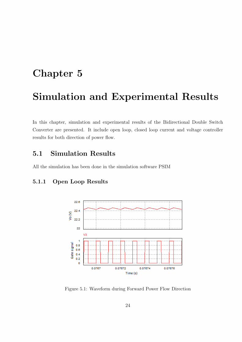
5.1 Waveform during Forward Power Flow Direction . . . . . . . . . . . . . . . . 24
5.2 Waveform during Reverse Power Plow Direction . . . . . . . . . . . . . . . . 25
5.3 Step Response of Controller during Forward Power Flow Direction . . . . . . 25
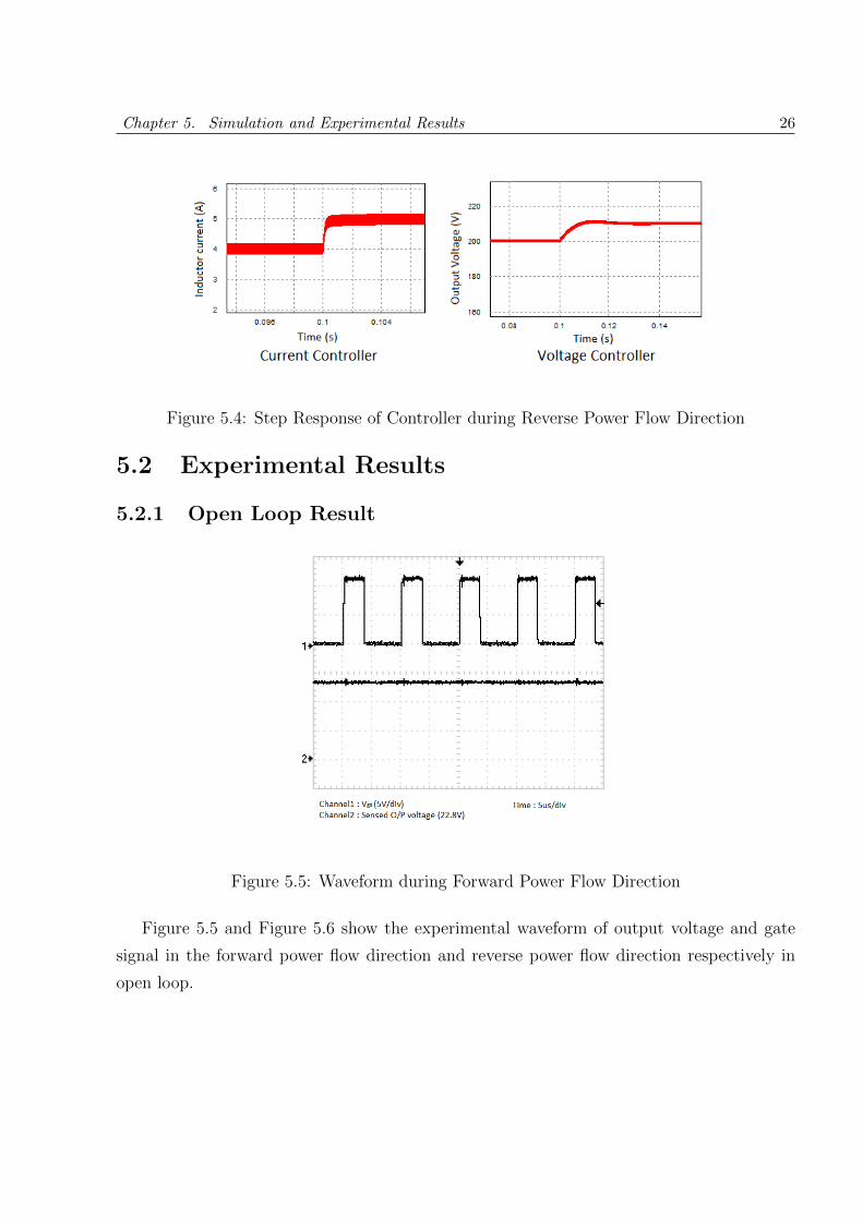
5.4 Step Response of Controller during Reverse Power Flow Direction . . . . . . 26
5.5 Waveform during Forward Power Flow Direction . . . . . . . . . . . . . . . . 26
viii
Page 10
List of Figures ix
5.6 Waveform during Reverse Power Flow Direction . . . . . . . . . . . . . . . . 27
5.7 Step Change in Current during Forward Power Flow Direction . . . . . . . . 27
5.8 Step Change in Voltage during Forward Power Flow Direction . . . . . . . . 28
5.9 Current controller during Reverse Power Flow Direction . . . . . . . . . . . . 28
A.1 dsPIC30F2023 Schematic Diagram . . . . . . . . . . . . . . . . . . . . . . . 31
A.2 Power Circuit Board Schematic Diagram - Primary Side . . . . . . . . . . . 32
A.3 Power Circuit Board Schematic Diagram - Secondary Side . . . . . . . . . . 32
Page 11
Nomenclature
Symbols : Definitions
Vb : Battery voltage
Ts : Switching period
d : Duty ratio
n : Turns ratio of transformer
e(n) : Error signal to PI controller
Ac : Area of core
Aw : Area of winding
aw : Area of wire
kw : Winding factor
J : Operating current density for copper
Bm : Peak flux density of inductor core
x
Page 12
Chapter 1
Introduction
The bidirectional dc-dc converter along with energy storage has become a promising option
for many power related systems, including hybrid vehicle, fuel cell vehicle, renewable energy
system and so forth. It not only reduces the cost and improves efficiency, but also improves
the performance of the system.
In the electric vehicle applications, an auxiliary energy storage battery absorbs the regen-
erated energy fed back by the electric machine. In addition, bidirectional dc-dc converter is
also required to draw power from the auxiliary battery to boost the high-voltage bus during
vehicle starting, accelerate and hill climbing. With its ability to reverse the direction of the
current flow, and thereby power, the bidirectional dc-dc converters are being increasingly
used to achieve power transfer between two dc power sources in either direction.
Recently, clean energy resources such as photovoltaic arrays and wind turbines have been
exploited for developing renewable electric power generation systems. The bidirectional
dc-dc converter is often used to transfer the solar energy to the capacitive energy source
during the sunny time, while to deliver energy to the load when the dc bus voltage is low.
The bidirectional dc-dc converter is regulated by the solar array photovoltaic level, thus to
maintain a stable load bus voltage and make fully usage of the solar array and the storage
battery.
Numerous topology for possible implementation as bidirectional DC-DC converters have
been reported so far [1]. Basically they are divided into two type, non-isolated and isolated
converters meetind different application requirements.
In isolated DC-DC bidirectional converter, isolation is normally provided by a trans-
former. The added transformer cause additional cost and losses. However, since transformer
can isolate the two side of the converter and provide the impedance matching between them.
1
Page 13
Chapter 1. Introduction 2
Also for high voltage ratio between two sides of converter, efficiency of non-isolated DC-
DC bidirectional converter is very poor. So Isolated idirectional DC-DC converter is an
alternative in those kinds of applications.
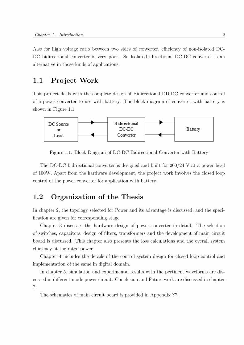
1.1 Project Work
This project deals with the complete design of Bidirectional DD-DC converter and control
of a power converter to use with battery. The block diagram of converter with battery is
shown in Figure 1.1.
Figure 1.1: Block Diagram of DC-DC Bidirectional Converter with Battery
The DC-DC bidirectional converter is designed and built for 200/24 V at a power level
of 100W. Apart from the hardware development, the project work involves the closed loop
control of the power converter for application with battery.
1.2 Organization of the Thesis
In chapter 2, the topology selected for Power and its advantage is discussed, and the speci-
fication are given for corresponding stage.
Chapter 3 discusses the hardware design of power converter in detail. The selection
of switches, capacitors, design of filters, transformers and the development of main circuit
board is discussed. This chapter also presents the loss calculations and the overall system
efficiency at the rated power.
Chapter 4 includes the details of the control system design for closed loop control and
implementation of the same in digital domain.
In chapter 5, simulation and experimental results with the pertinent waveforms are dis-
cussed in different mode power circuit. Conclusion and Future work are discussed in chapter
7
The schematics of main circuit board is provided in Appendix ??.
Page 14
Chapter 2
Toplology Selection and Specification
In this chapter, Non-isolated topology and topology for isolated bidirectional DC-DC con-
verter is selected among the available topologies and their specification in terms of power,
voltage and switching frequency are specified.
2.1 Non-isolated Bidirectional DC-DC Converter
Vi
S1
S2
L
Vb
C
Figure 2.1: Circuit Diagram of Non-isolated DC-DC Bidirectional Converter[1]
The circuit diagram of basic non-isolated bidirectional converter is shown in Figure 2.1.
The function of circuit is as follows,
3
Page 15
Chapter 2. Toplology Selection and Specification 4
Buck Mode: In this mode of operation only Switch S1 is switched corresponding to required
voltage. When S1 is off, inductor current freewheels through antiparallel diode of switch
S2. For duty ratio d,
Vb = Vi d (2.1)
Boost Mode: In this mode of operation only Switch S2 is switched corresponding to re-
quired voltage. When S2 is off, inductor current flow through antiparallel diode of
switch S1. For duty ratio d,
Vi =Vb
1− d(2.2)
For high voltage turns ratio between two sides of converter, the duty ratio has to be high,
so the efficiency will be poor.
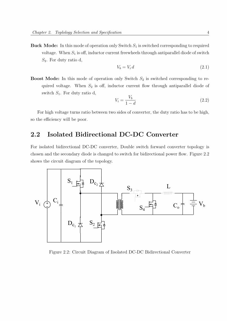
2.2 Isolated Bidirectional DC-DC Converter
For isolated bidirectional DC-DC converter, Double switch forward converter topology is
chosen and the secondary diode is changed to switch for bidirectional power flow. Figure 2.2
shows the circuit diagram of the topology.
Vi
S1
S2
L
VbCi
S3
S4Co
Dc2
Dc1
Figure 2.2: Circuit Diagram of Iisolated DC-DC Bidirectional Converter
Page 16
Chapter 2. Toplology Selection and Specification 5
Advantage of this topology compared to other isolated toplogy are the following
• As there is no reset winding, transformer design is simple
• Device voltage rating in the primary side is same as the DC bus voltage
• Clamp diodes recover magnetising energy in the core and it is fed back to supply
In the forward direction of power flow, both switches S1 and S2 gets the same PWM and
secondary switches is not given PWM. During the ON time of S1 and S2 antiparallel diode
of switch S3 will be forward biased, during OFF time inductor current freewheels through
the antiparallel diode of switch S4. For duty ratio d and turns ratio n,
Vb = Vi n d (2.3)
In the reverse direction of power flow, the switches S3 and S4 are given complementary
PWM signals. The voltage at the load side is given by
Vi =Vb
n(1− d)(2.4)
The limitation of the circuit is that two power switches are needed with the associated
drive circuits and unidirectional flux swing in the core which limits the maximum duty cycle
of switch S1 and S2to 50% during forward power flow direction to avoid core saturation.
Similarly minimum duty ratio of S4 is limited to 50% during reverse power flow direction.
Bidirectional double switch forward converter is designed for 100W output power and
200/24 V. Switching frequency of switches S1 and S2 are chosen to be 100 kHz to reduce
the sizes of transformer and filter components.
Page 17
Chapter 3
Hardware Design
The hardware design of the double Switch bidirectional converter power circuit is explained
in this chapter. It includes the selection of switches, design and construction of filter induc-
tor and transformer, and design of snubber circuit.The efficiency and loss calculations are
presented. The development of the complete circuit board is also discussed.
3.1 System Ratings
Vi
S1
S2
L
VbCi
S3
S4Co
Dc2
Dc1
Figure 3.1: Power Circuit Topology for the Bidirectional Double Switch Forward Converter
The power circuit topology is shown in Figure 3.1 which is meant to be used for charging
the battery from a DC source of different voltage level and giving power from battery to a
load of different voltage level. The rating of the power circuit is given in the Table 3.1. The
switching frequency is chosen as 100kHz.
6
Page 18
Chapter 3. Hardware Design 7
Component Rated value
Input Voltage 200V
Output voltage 24V
Power 100W
Table 3.1: Ratings of Power Converter
3.2 Power Circuit Design
First, a double switch forward converter (as shown in the Figure 3.2) is designed for system
rating and then modified the circuit for bidirectional power supply. It include transformer
design, filter component design and switch selection.
Vi
S1
S2
L
VbCi
D1
Co
Dc2
Dc1
D2
Figure 3.2: Circuit Diagram of Double Switch Forward Converter
3.2.1 Design of Transformer
For an input voltage, Vi = 24V and output voltage, Vo = 200V at a power level, P = 100W
and duty ratio d = 0.35 turns ratio of transformer is given by
N1
N2
=Vid
Vo(3.1)
gives N1
N2= 3.
Page 19
Chapter 3. Hardware Design 8
Using area product approach [2] we can find that
AcAw =2Vidmaxis1rms
∆BKwJfs(3.2)
where Ac and Aw are cross sectional area of core and window area respectively, dmax is
maximum duty ratio possible, is1rms is rms current of primary winding, ∆B is change in
magnetic field, Kw is window space factor of core, J is current density of wire and fs is
switching frequency. With Vi = 200V , dmax = 0.5, is1rms = 10024
13
√0.5 = 0.982A, ∆B =
0.25T , Kw = 0.3, J = 3A/mm2 and fs = 100kHz
AcAw = 0.872cm4
ETD39 [8] with Ac = 1.25mm2 and Aw = 1.78mm2 is chosen. Now
N1 =Vidmax
∆BfsAc(3.3)
gives N1 = 33, so N2 = 11.
The size of winding wire is chosen by using
aw =IrmsJ
(3.4)
which gives aw1 = 0.33mm2 and aw2 = 0.98mm2, where aw1 and aw2 are the cross sec-
tional areae of primary and secondary windings. SWG21 with aw = 0.5189mm2 and
R = 33.23Ω/km for primary winding and SWG15 with aw = 2.627mm2 and R = 6.564Ω/km
for secondary winding are selected.
The used core material is N87 which is having µr ' 2000, and mean length of flux path,
lm = 92.2mm. Therfore it is obtained that Lm−p ' 3.72mH and im−p = 0.19A using
Lm−p =µ0µrAcN1
2
lm(3.5)
and
im−p =Vi
Lm−pdTs (3.6)
respectively. Also mean length of turn, lm ' 69mm, so Rp = 33.23 ∗ 69 ∗ 10−6 ∗ 33 = 75mΩ,
similarly Rs = 4.98mΩ. Therfore copper loss is obtained as 0.116W by using
Page 20
Chapter 3. Hardware Design 9
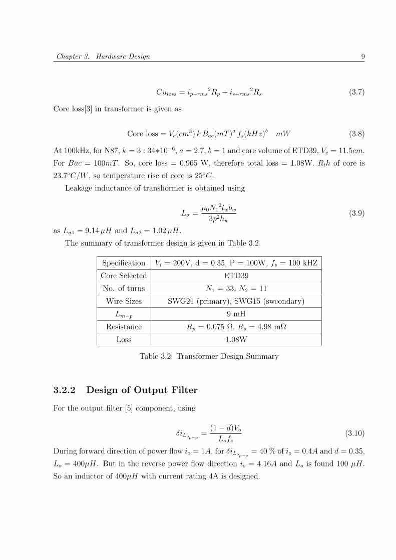
Culoss = ip−rms2Rp + is−rms
2Rs (3.7)
Core loss[3] in transformer is given as
Core loss = Vc(cm3) k Bac(mT )a fs(kHz)b mW (3.8)
At 100kHz, for N87, k = 3 : 34∗10−6, a = 2.7, b = 1 and core volume of ETD39, Vc = 11.5cm.
For Bac = 100mT . So, core loss = 0.965 W, therefore total loss = 1.08W. Rth of core is
23.7C/W , so temperature rise of core is 25C.
Leakage inductance of transhormer is obtained using
Lσ =µ0N1
2lwbw3p2hw
(3.9)
as Lσ1 = 9.14µH and Lσ2 = 1.02µH.
The summary of transformer design is given in Table 3.2.
Specification Vi = 200V, d = 0.35, P = 100W, fs = 100 kHZ
Core Selected ETD39
No. of turns N1 = 33, N2 = 11
Wire Sizes SWG21 (primary), SWG15 (swcondary)
Lm−p 9 mH
Resistance Rp = 0.075 Ω, Rs = 4.98 mΩ
Loss 1.08W
Table 3.2: Transformer Design Summary
3.2.2 Design of Output Filter
For the output filter [5] component, using
δiLop−p=
(1− d)VoLofs
(3.10)
During forward direction of power flow io = 1A, for δiLop−p= 40 % of io = 0.4A and d = 0.35,
Lo = 400µH. But in the reverse power flow direction io = 4.16A and Lo is found 100 µH.
So an inductor of 400µH with current rating 4A is designed.
Page 21
Chapter 3. Hardware Design 10
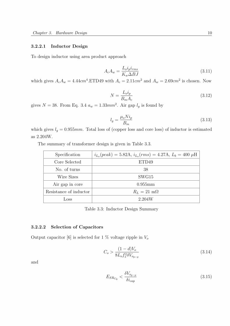
3.2.2.1 Inductor Design
To design inductor using area product approach
AcAw =LoipirmsKw∆BJ
(3.11)
which gives AcAw = 4.44cm4.ETD49 with Ac = 2.11cm2 and Aw = 2.69cm2 is chosen. Now
N =LoipBmAc
(3.12)
gives N = 38. From Eq. 3.4 aw = 1.33mm2. Air gap lg is found by
lg =µoNipBm
(3.13)
which gives lg = 0.955mm. Total loss of (copper loss and core loss) of inductor is estimated
as 2.204W.
The summary of transformer design is given in Table 3.3.
Specification iLo(peak) = 5.82A, iLo(rms) = 4.27A, Lb = 400 µH
Core Selected ETD49
No. of turns 38
Wire Sizes SWG15
Air gap in core 0.955mm
Resistance of inductor RL = 21 mΩ
Loss 2.204W
Table 3.3: Inductor Design Summary
3.2.2.2 Selection of Capacitors
Output capacitor [6] is selected for 1 % voltage ripple in Vo
Co >(1− d)Vo
8Lof 2s δVop−p
(3.14)
and
ESRC0<δVop−p
δicap(3.15)
Page 22
Chapter 3. Hardware Design 11
give Co > 2µF and ESRC0< 0.12Ω. A capacitor of 1000 µF with 0.1 Ω is chosen. Similarly
for the reverse direction of power flow input capacitor is selected as
Ci >ii(1− d)
δVifs(3.16)
give Ci = 63µF and ESRC0< 0.85Ω. A capacitor of 100 µF with 0.75 Ω is chosen.
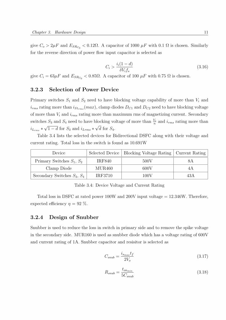
3.2.3 Selection of Power Device
Primary switches S1 and S2 need to have blocking voltage capability of more than Vi and
irms rating more than iS1rms(max), clamp diodes DC1 and DC2 need to have blocking voltage
of more than Vi and irms rating more than maximum rms of magnetizing current. Secondary
switches S3 and S4 need to have blocking voltage of more than Vin
and irms rating more than
iLrms ∗√
1− d for S3 and iLrms ∗√d for S4.
Table 3.4 lists the selected devices for Bidirectional DSFC along with their voltage and
current rating. Total loss in the switch is found as 10.691W
Device Selected Device Blocking Voltage Rating Current Rating
Primary Switches S1, S2 IRF840 500V 8A
Clamp Diode MUR460 600V 4A
Secondary Switches S3, S4 IRF3710 100V 43A
Table 3.4: Device Voltage and Current Rating
Total loss in DSFC at rated power 100W and 200V input voltage = 12.346W. Therefore,
expected efficiency η = 92 %.
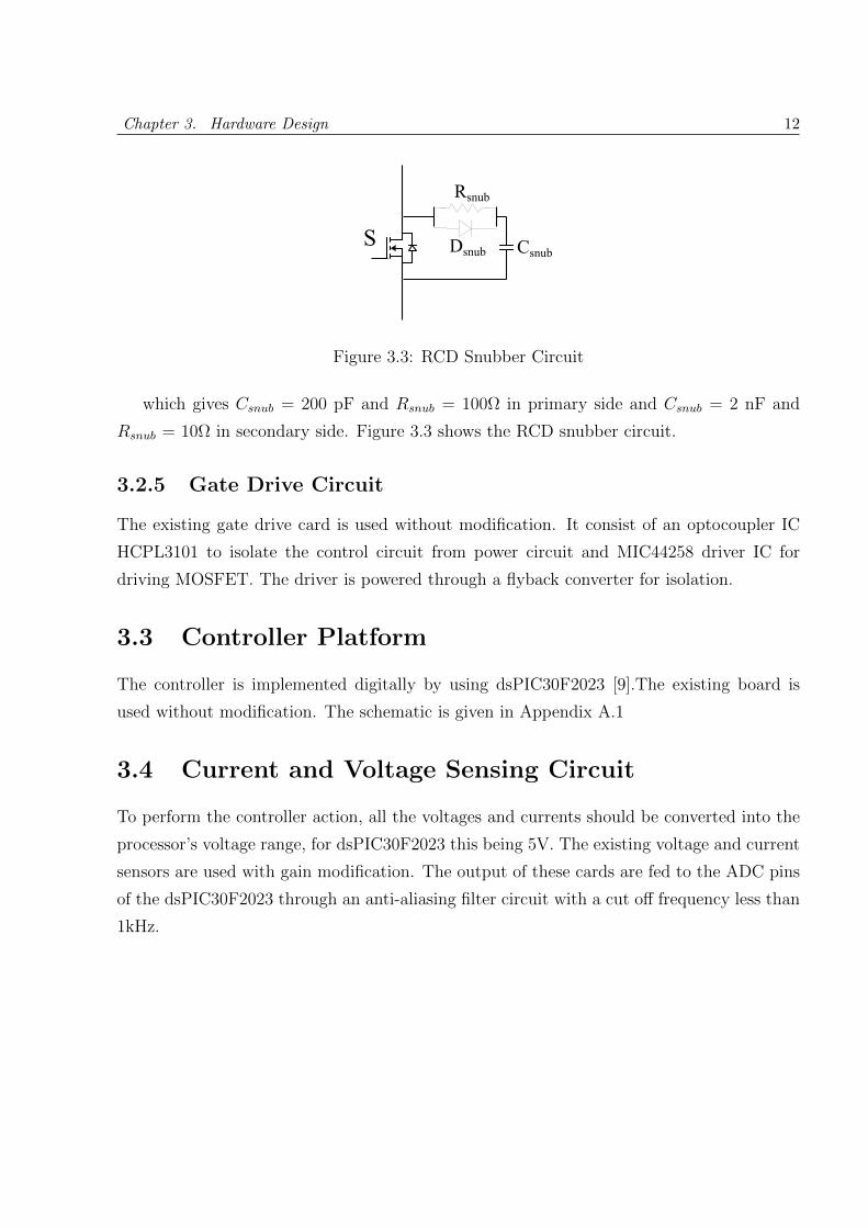
3.2.4 Design of Snubber
Snubber is used to reduce the loss in switch in primary side and to remove the spike voltage
in the secondary side. MUR160 is used as snubber diode which has a voltage rating of 600V
and current rating of 1A. Snubber capacitor and resisitor is selected as
Csnub =ismaxtf
2Vo(3.17)
Rsnub =tonmin
5Csnub(3.18)
Page 23
Chapter 3. Hardware Design 12
S
Rsnub
CsnubDsnub
Figure 3.3: RCD Snubber Circuit
which gives Csnub = 200 pF and Rsnub = 100Ω in primary side and Csnub = 2 nF and
Rsnub = 10Ω in secondary side. Figure 3.3 shows the RCD snubber circuit.
3.2.5 Gate Drive Circuit
The existing gate drive card is used without modification. It consist of an optocoupler IC
HCPL3101 to isolate the control circuit from power circuit and MIC44258 driver IC for
driving MOSFET. The driver is powered through a flyback converter for isolation.
3.3 Controller Platform
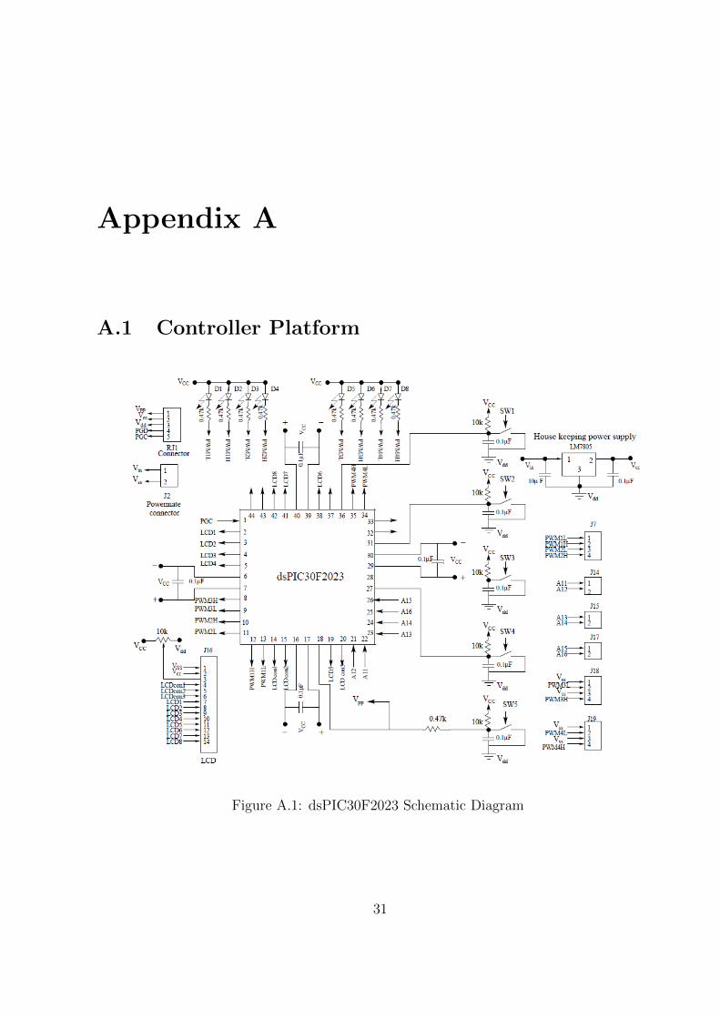
The controller is implemented digitally by using dsPIC30F2023 [9].The existing board is
used without modification. The schematic is given in Appendix A.1
3.4 Current and Voltage Sensing Circuit
To perform the controller action, all the voltages and currents should be converted into the
processor’s voltage range, for dsPIC30F2023 this being 5V. The existing voltage and current
sensors are used with gain modification. The output of these cards are fed to the ADC pins
of the dsPIC30F2023 through an anti-aliasing filter circuit with a cut off frequency less than
1kHz.
Page 24
Chapter 3. Hardware Design 13
3.5 Conclusion
The bidirectional double switch forward converter was designed and built for 100W power
level. Snubber circuit was designed to reduce the voltage stress across the secondary switch.
For the implementation of PWM signal and controller dsPIC30F2023 was used.
Page 25
Chapter 4
Controller Design
This chapter discusses the design of current and voltage controllers for the power circuit,
their transformation to the z-domain and finally digital implementation of these controllers
in dsPIC30F2023 microcontroller through C programming.
4.1 Closed Loop Control
The closed loop control is done to prevent variations in the output voltage or output current,
due to any disturbances, by introducing a control variable in the form of duty ratio. This
control variable d, is used to turn on the active devices in the switching circuits for a duration
corresponding to its value. Closed loop control varies the duty ratio, in case of any deviation
in output parameter, from its present steady state value to a new steady state value and
thereby correcting the variation in the output.
4.1.1 Control Objective
The main objective of closed loop controller are the following
1. Steady state accuracy: The steady state error should be less than 1%. For that DC
gain of the system is set to be very high.
2. Settling time in response to disturbance: Any disturbance in the input affect
the output of system. The time to respond to this variation should be small.
ie is bandwidth is to be set as high.
14
Page 26
Chapter 4. Controller Design 15
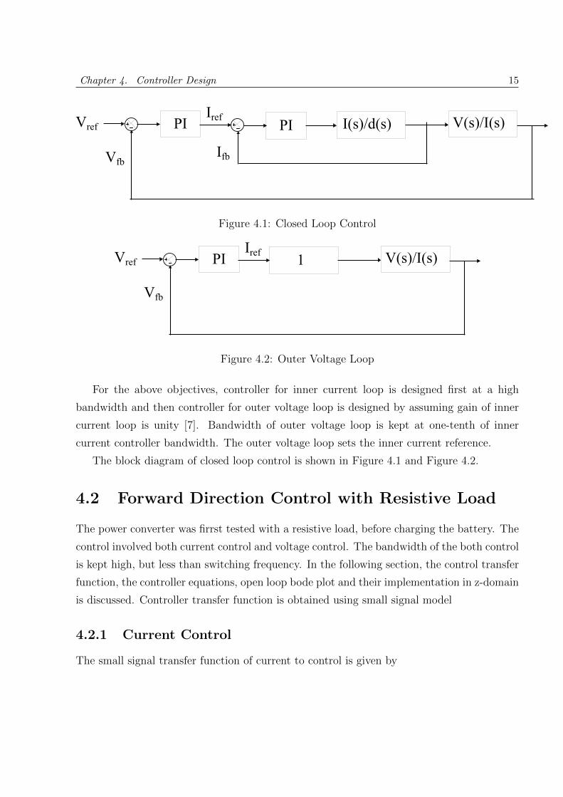
PIVref
Vfb
PIIref
Ifb
I(s)/d(s) V(s)/I(s)
Figure 4.1: Closed Loop Control
PIVref
Vfb
Iref V(s)/I(s)1
Figure 4.2: Outer Voltage Loop
For the above objectives, controller for inner current loop is designed first at a high
bandwidth and then controller for outer voltage loop is designed by assuming gain of inner
current loop is unity [7]. Bandwidth of outer voltage loop is kept at one-tenth of inner
current controller bandwidth. The outer voltage loop sets the inner current reference.
The block diagram of closed loop control is shown in Figure 4.1 and Figure 4.2.
4.2 Forward Direction Control with Resistive Load
The power converter was firrst tested with a resistive load, before charging the battery. The
control involved both current control and voltage control. The bandwidth of the both control
is kept high, but less than switching frequency. In the following section, the control transfer
function, the controller equations, open loop bode plot and their implementation in z-domain
is discussed. Controller transfer function is obtained using small signal model
4.2.1 Current Control
The small signal transfer function of current to control is given by
Page 27
Chapter 4. Controller Design 16
g(s) =il(s)
d(s)=
VinR
(1 + sCoR)
(1 + sLR
+ s2LCo)(4.1)
The bode plot of this transfer function with the experimental values of Vi = 200 V, n =
3, R = 24 Ω, Co = 1000 µF, L = 300 µ is shown in Figure 4.3 and
g(s) =il(s)
d(s)= 2.78
(1 + s41.67
)
(1 + s60000
+ s2
2500000)
PI controller is designed for a bandwidth of 10000 rad/sec. The transfer function of the
PI controller used is
h(s) =1 + s
1580s
100
(4.2)
The bode plot of the loop gain GH is given in Figure 4.4. The digital implementation of
the above PI controller is done using bilinear transformation. The controller implemented
with a sampling frequency of 10kHz is
kp[n] = 0.0625 ∗ error[n] (4.3)
ki[n] = ki[n− 1] + 0.005 ∗ error[n] + 0.005 ∗ error[n− 1] (4.4)
d[n] = kp[n] + ki[n] (4.5)
4.2.2 Voltage Control
The small signal transfer function of voltage to current is given by
g(s) =vo(s)
il(s)=
R
1 + sRCo(4.6)
g(s) =vo(s)
il(s)=
24
1 + s41.67
The bode plot of this transfer function with the experimental values is shown in Figure
4.5. The transfer function of the controller used is
h(s) =1 + s
41.67s50
(4.7)
Page 28
Chapter 4. Controller Design 17
Figure 4.3: Current to Duty Ratio Transfer Function il(s)
d(s)
Figure 4.4: Current Control Loop Gain Transfer Function
Page 29
Chapter 4. Controller Design 18
Figure 4.5: Voltage to Current Transfer Function vo(s)
il(s)
Figure 4.6: Voltage Control Loop Gain Transfer Function
Page 30
Chapter 4. Controller Design 19
The bode plot of the loop gain GH is given in Figure 4.6. The above controller in digital
domain is
kp[n] = 1.2 ∗ error[n] (4.8)
ki[n] = ki[n− 1] + 0.0025 ∗ error[n] + 0.0025 ∗ error[n− 1] (4.9)
iref [n] = kp[n] + ki[n] (4.10)
4.3 Reverse Direction Control
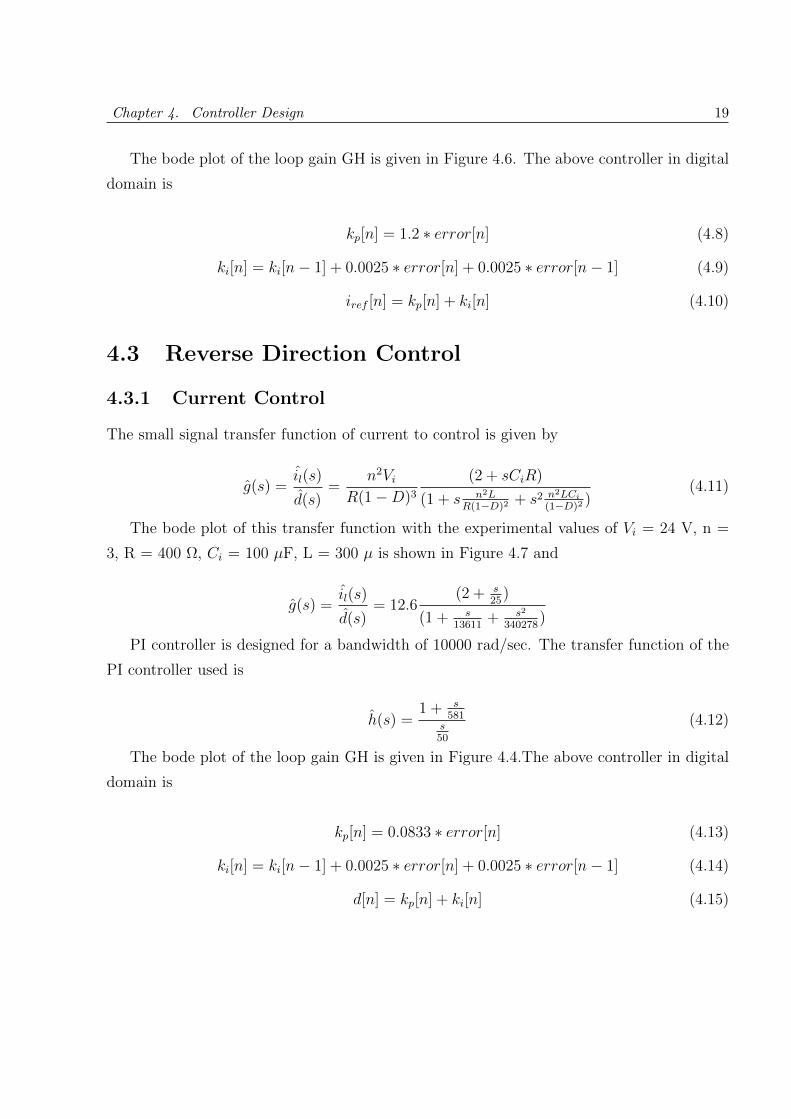
4.3.1 Current Control
The small signal transfer function of current to control is given by
g(s) =il(s)
d(s)=
n2ViR(1−D)3
(2 + sCiR)
(1 + s n2LR(1−D)2
+ s2 n2LCi
(1−D)2)
(4.11)
The bode plot of this transfer function with the experimental values of Vi = 24 V, n =
3, R = 400 Ω, Ci = 100 µF, L = 300 µ is shown in Figure 4.7 and
g(s) =il(s)
d(s)= 12.6
(2 + s25
)
(1 + s13611
+ s2
340278)
PI controller is designed for a bandwidth of 10000 rad/sec. The transfer function of the
PI controller used is
h(s) =1 + s
581s50
(4.12)
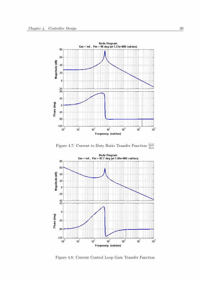
The bode plot of the loop gain GH is given in Figure 4.4.The above controller in digital
domain is
kp[n] = 0.0833 ∗ error[n] (4.13)
ki[n] = ki[n− 1] + 0.0025 ∗ error[n] + 0.0025 ∗ error[n− 1] (4.14)
d[n] = kp[n] + ki[n] (4.15)
Page 31
Chapter 4. Controller Design 20
Figure 4.7: Current to Duty Ratio Transfer Function il(s)
d(s)
Figure 4.8: Current Control Loop Gain Transfer Function
Page 32
Chapter 4. Controller Design 21
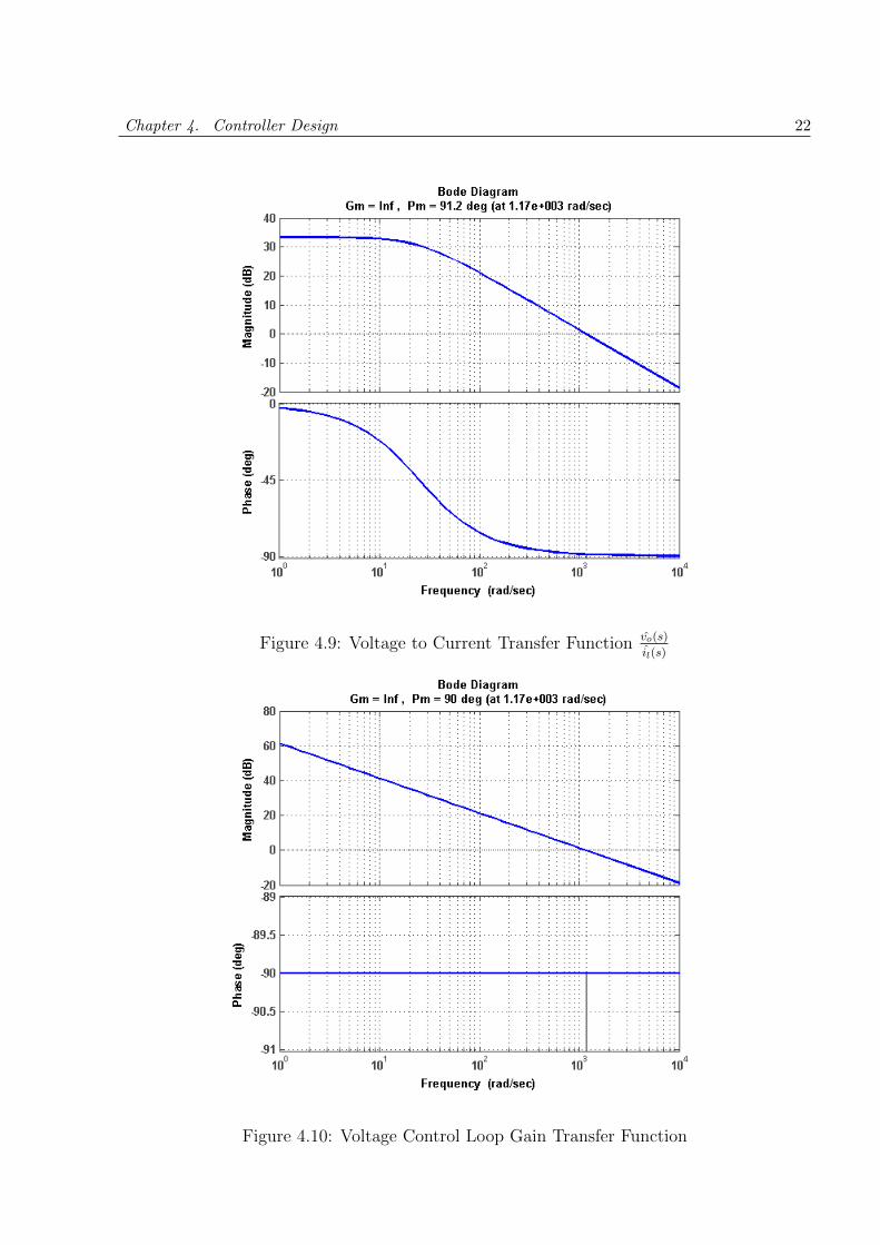
4.3.2 Voltage Control
The small signal transfer function of voltage to currentl is given by
g(s) =vo(s)
il(s)=nR(1−D)
1 + sCiR(4.16)
g(s) =vo(s)
il(s)=
46.67
1 + s25
The bode plot of this transfer function with the experimental values is shown in Figure
4.9. The transfer function of the controller used is
h(s) =1 + s
25s25
(4.17)
The bode plot of the loop gain GH is given in Figure 4.10. The above controller in digital
domain is
kp[n] = 1 ∗ error[n] (4.18)
ki[n] = ki[n− 1] + 0.00125 ∗ error[n] + 0.00125 ∗ error[n− 1] (4.19)
iref [n] = kp[n] + ki[n] (4.20)
Page 33
Chapter 4. Controller Design 22
Figure 4.9: Voltage to Current Transfer Function vo(s)
il(s)
Figure 4.10: Voltage Control Loop Gain Transfer Function
Page 34
Chapter 4. Controller Design 23
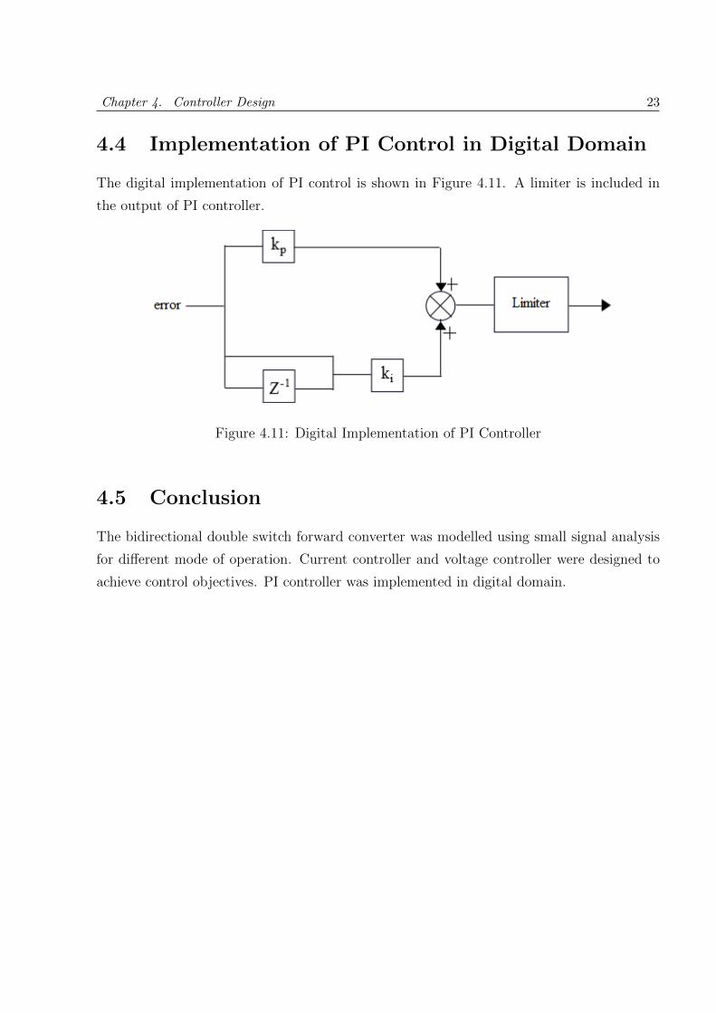
4.4 Implementation of PI Control in Digital Domain
The digital implementation of PI control is shown in Figure 4.11. A limiter is included in
the output of PI controller.
Figure 4.11: Digital Implementation of PI Controller
4.5 Conclusion
The bidirectional double switch forward converter was modelled using small signal analysis
for different mode of operation. Current controller and voltage controller were designed to
achieve control objectives. PI controller was implemented in digital domain.
Page 35
Chapter 5
Simulation and Experimental Results
In this chapter, simulation and experimental results of the Bidirectional Double Switch
Converter are presented. It include open loop, closed loop current and voltage controller
results for both direction of power flow.
5.1 Simulation Results
All the simulation has been done in the simulation software PSIM
5.1.1 Open Loop Results
Figure 5.1: Waveform during Forward Power Flow Direction
24
Page 36
Chapter 5. Simulation and Experimental Results 25
Figure 5.2: Waveform during Reverse Power Plow Direction
The output voltage waveform with switching signal is shown in Figure 5.1 and Figure 5.2
for forward and reverse power flow direction respectively.
5.1.2 Closed Loop Results
Figure 5.3: Step Response of Controller during Forward Power Flow Direction
Figure 5.3 and Figure 5.4 shows the response of current and voltage controllers for a step
change in corresponding referances in forward and reverse direction respectively.
Page 37
Chapter 5. Simulation and Experimental Results 26
Figure 5.4: Step Response of Controller during Reverse Power Flow Direction
5.2 Experimental Results
5.2.1 Open Loop Result
Figure 5.5: Waveform during Forward Power Flow Direction
Figure 5.5 and Figure 5.6 show the experimental waveform of output voltage and gate
signal in the forward power flow direction and reverse power flow direction respectively in
open loop.
Page 38
Chapter 5. Simulation and Experimental Results 27
Figure 5.6: Waveform during Reverse Power Flow Direction
5.2.2 Closed Loop Results
Figure 5.7: Step Change in Current during Forward Power Flow Direction
Figure 5.7 shows the response of current controller mode to a step change of current
referance from 0.5A to 1A in forward direction of power flow with resistive load.
Page 39
Chapter 5. Simulation and Experimental Results 28
Figure 5.8: Step Change in Voltage during Forward Power Flow Direction
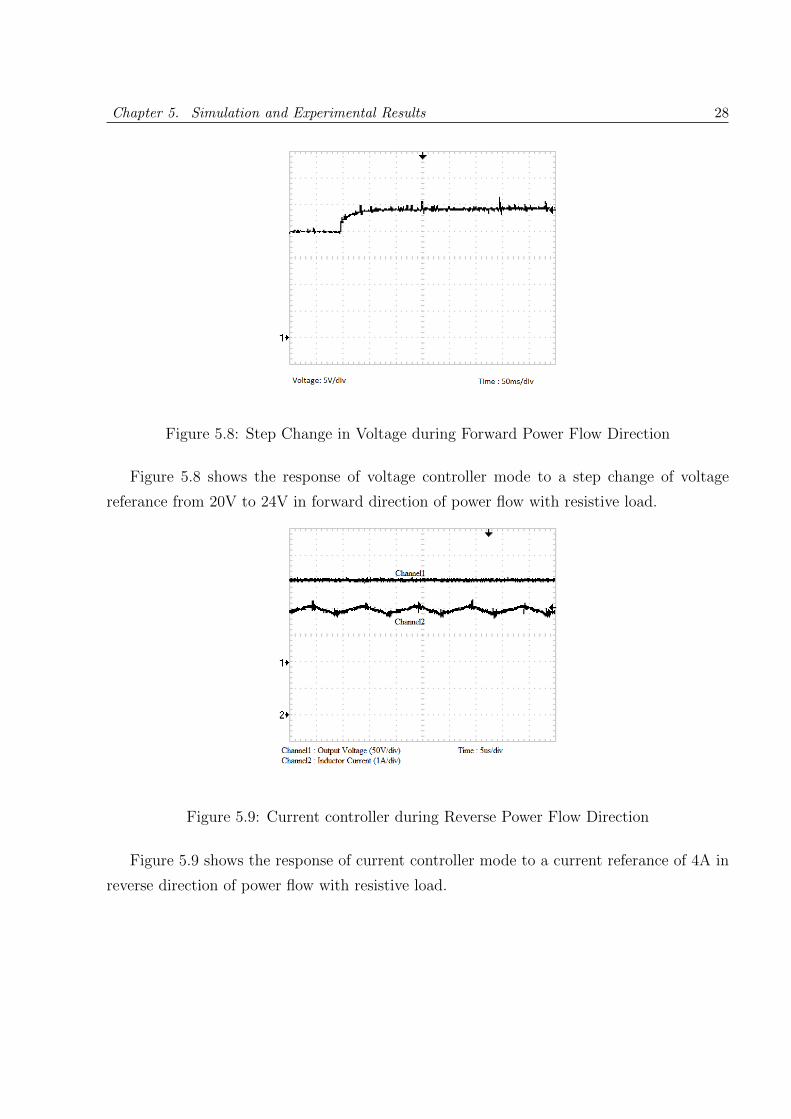
Figure 5.8 shows the response of voltage controller mode to a step change of voltage
referance from 20V to 24V in forward direction of power flow with resistive load.
Figure 5.9: Current controller during Reverse Power Flow Direction
Figure 5.9 shows the response of current controller mode to a current referance of 4A in
reverse direction of power flow with resistive load.
Page 40
Chapter 5. Simulation and Experimental Results 29
5.2.3 Efficiency of Converter
Table 5.1 and Table 5.2 show the efficiency of the double switch bidirectional forward con-
verter during forward and reverse direction of power flow at different power level.
Power (W) Efficiency (%)
25 96.25
50 92.92
75 89.56
100 86.95
Table 5.1: Efficiency During Forward Power Flow at Different Power Level
Power (W) Efficiency (%)
50 91.83
75 88.41
100 86.72
Table 5.2: Efficiency During Reverse Power Flow at Different Power Level
5.3 Conclusion
The bidirectional double switch forward converter is tested in PSIM simulation software and
experimentally. Both the results were found to be matching.
Page 41
Chapter 6
Conclusions
The project was aimed at developing the hardware for Isolated Bidirectional DC-DC con-
verter and close loop control for battery charging and discharging. The hardware built for
the project consists of:
1. Power circuit board.
2. The magnetic components - inductors and transformer
First the bidirectional double switch forward converter was designed and validated in
simulation software PSIM. By using the bidirectional switch and appropriate switching the
power flow in the bidirectional double switch forward converter can be controlled. The
direction of power flow is decided by current flow direction. The controller is designed for
controlling both current and voltage and experimentally validated for forward direction of
power flow.
30
Page 42
Appendix A
A.1 Controller Platform
Figure A.1: dsPIC30F2023 Schematic Diagram
31
Page 43
Appendix A. 32
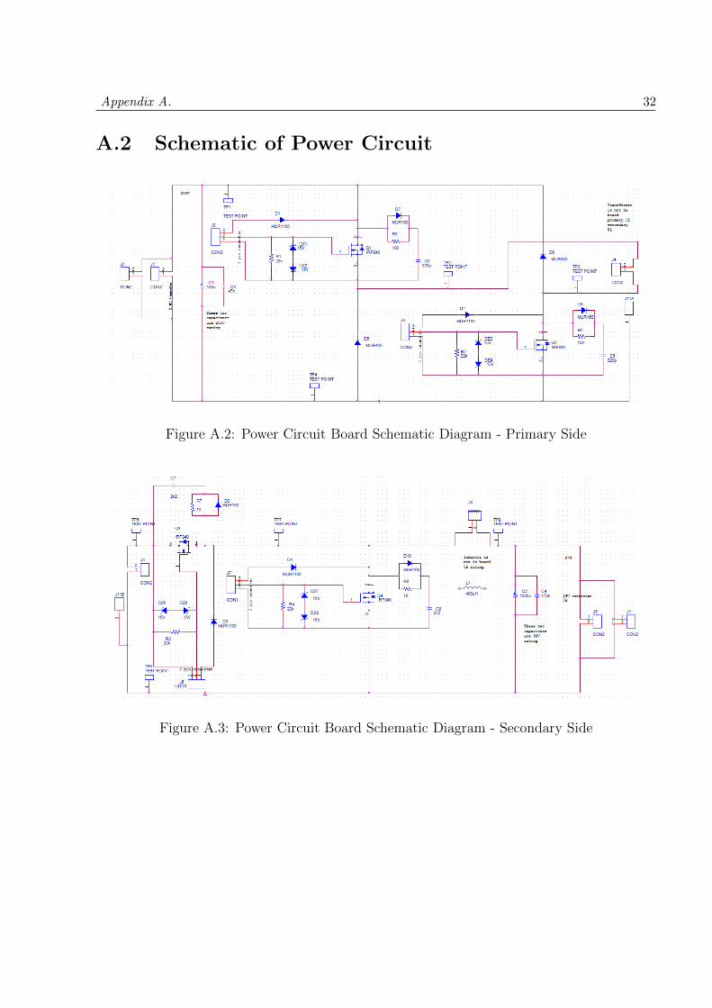
A.2 Schematic of Power Circuit
Figure A.2: Power Circuit Board Schematic Diagram - Primary Side
Figure A.3: Power Circuit Board Schematic Diagram - Secondary Side
Page 44
References
[1] Junhong Zhang, “Bidirectional DC-DC Power Converter Design Optimization, Modeling
and Control”, PhD Thesis, Virginia Polytechnic Institute and State University.
[2] Ramanarayanan. V,“Course Material on Switched Mode Power Conversion”,Dept. of
Electrical Engineering, Indian Institute of Science,Bangalore
[3] Akshay Kumrawat, “Design of Control Power Supply for High Power Converters with
wide Input Variation”, ME Thesis, Department of Electrical Engineering, Indian Institute
of Science, Bangalore 2011.
[4] J.-S. Lai and D. J. Nelson, “Energy management power converters in hybrid electric and
fuel cell vehicles,” in Proc. IEEE Ind. Electron., Taipei, Taiwan, Volume 95, Issue 4,
April 2007, pp. 766 777.
[5] G. Narayanan, “Class notes of Power Electronics”, Department of Electrical Engineering,
Indian Institute of Science, Bangalore, 2011.
[6] Vinod John, “Class notes of Topics in Power Electronics and Distributed Generation”,
Department of Electrical Engineering, Indian Institute of Science, Bangalore, 2012.
[7] Anand Vivek Ravi, “Control Power Supply Architecture For Ride Through in Power
Converters using Ultra-capacitors”, ME report, Department of Electrical Engineering,
Indian Institute of Science, Bangalore, 2010.
[8] website “http://www.epcos.com”.
[9] dsPIC30F Family Reference manual, “http://www.microchip.com”.
[10] IRF540N datasheet ,International Rectfier, “http://www.irf.com”.
33
Page 45
References 34
[11] IRF3710 datasheet ,International Rectfier, “http://www.irf.com”.


![HIGH-CONVERSION-RATIO BIDIRECTIONAL DC–DC ......bidirectional dc –dc converter with a high convention ratio is a key component of battery applications [5] Isolated bidirectional](https://static.documents.pub/doc/80x56/5f0a32787e708231d42a7b2d/high-conversion-ratio-bidirectional-dcadc-bidirectional-dc-adc-converter.jpg)


