+ All Categories
Home > Documents > BiFeO3 - CoFe2O4 nanostructured multiferroic thin filmsphdthesis.uaic.ro/PhDThesis/Stratulat,...

BiFeO3 - CoFe2O4 nanostructured multiferroic thin filmsphdthesis.uaic.ro/PhDThesis/Stratulat,...

Date post: 13-Jul-2018
Category:
Upload: lekhanh
View: 227 times
Download: 0 times
Share this document with a friend
33
BiFeO3 - CoFe2O4 nanostructured multiferroic thin films Sergiu Mihai Stratulat Supervisor dr. Marin Alexe Supervisor prof. dr. Ovidiu Florin Călțun Iași, 2013 Universitatea Alexandru Ioan Cuza, Facultatea de Fizică
Transcript

BiFeO3 - CoFe2O4

nanostructured multiferroic

thin films

Sergiu Mihai Stratulat

Supervisor

dr. Marin Alexe

Supervisor

prof. dr. Ovidiu Florin Călțun

Iași, 2013

Universitatea Alexandru Ioan Cuza, Facultatea de Fizică

Contents Abstract ........................................................................................... 1

Acknowledgements .......................................................................... 3

Introduction ..................................................................................... 6

Chapter I. Magnetoelectric materials .............................................. 10

I.1 Single-phase magnetoelectrics ......................................................... 11

I.2 Hmagnetoelectric heterostructures .................................................. 12 I.2.1 Common materials for magnetoelectric thin films heterostructures ......... 16

I.3 Bismuth ferrite – BiFeO3 (BFO) ......................................................... 17 I.3.1 Ferroelectric properties .............................................................................. 19 I.3.2 Magnetic properties .................................................................................... 20 I.3.3 Electric properties ....................................................................................... 21 I.3.4 Magnetoelectric properties ........................................................................ 21

I.4 Aplications ...................................................................................... 22

Chapter II. Pulsed laser deposition of thin films ............................... 23

II.1 Target-laser interaction .................................................................. 25

II.2 Thin films’ growth modes................................................................ 28

II.3 Mechanisms and theories concerning thin films’ growth .................. 30 II.3.1 Adsorbtion theory ...................................................................................... 30 II.3.2 Thermodinamic theory ............................................................................... 31 II.3.3 Atomic or statistical theory ........................................................................ 32

II.4 Epitaxial growth ............................................................................. 33

Chapter III. Experimental techniques ............................................... 36

III.1 Atomic force miscroscopy .............................................................. 37

III.2 scanning electron miscroscopy ....................................................... 40

III.3 Magnetocapacitance measurements .............................................. 40

III.4 Raman spectroscopy ...................................................................... 42

Chapeter IV. Alternative route for obtaining NiFe2O4 thin films by

PLD................................................................................................. 44

IV.1 Introduction .................................................................................. 45

IV.2 Film deposition.............................................................................. 46

IV.3 Structural characterization ............................................................ 47

Chapter V. Nanostructured multiferroic system BiFeO3 – CoFe2O4 .. 53

V.1 Introduction ................................................................................... 54

V.2 Synthesis method ........................................................................... 56

V.3 Structural characterization ............................................................. 59

V.4 Functional characterization ............................................................. 65

V.5 Magnetoelectric coupling ............................................................... 69

Conclusions .................................................................................... 78

References ...................................................................................... 80

Communications and publications list: ............................................ 86

Introduction

The term “multiferroic” defines materials with at least two ferroic orders:

magnetism, ferroelectricity and ferroelasticity. Present days, this notion is widely

used to refer to the existence of magnetism and ferroelectricity and the coupling

between them. This magnetoelectric coupling offers the possibility of magnetically

controlling the electric polarization and electrically controlling the magnetization

[1,2] (figure 1), with applications that may arise in industries such as that of

sensors, transducers, magnetic memories, etc. [3,4].

This study was focused on the growth and characterization of

magnetoelectric heterostructures comprising BiFeO3 and CoFe2O4. We chose the

materials due to their individual properties, which make them suitable for these

kind of heterostructures (e.g. high piezoelectric coefficient, high

magnetostriction), and due to the synergy between them (e.g. similar crystalline

structure, low immiscibility). The aim of this work was the vertical type of

heterostructures (1-3 connectivity) consisting of magnetic pillars embedded in a

ferroelectric matrix. A special focus was set on developing a process that would

produce a highly ordered arrangement of these pillars.

The thesis is structured on 5 chapters: chapter I offers a broad overview

on magnetoelectric materials and also some properties of bismuth ferrite; chapter

II deals with the growth of thin films through pulsed laser deposition; in chapter

III, the characterization techniques are shortly described; chapter IV presents the

results for the alternative process of NiFe2O4 thin film growth; chapter V is

detailing the results for the growth and characterization of vertical

magnetoelectric heterostructures BiFeO3 – CoFe2O4.

1

Chapter I. Magnetoelectric materials

I.1 Single-phase multiferroic materials

The interest in single-phase multiferroics is having both magnetism and

ferroelectricity, and also the coupling between them. The biggest drawback is the

mutual exclusion of the mechanism for magnetism and the classical one for

ferroelectricity. Thus, for further study, several novel ferroelectricity origins have

been taken into account that would permit the existence of magnetic order.

I.2 Magnetoelectric heterostructures

The low number of single-phase multiferroics led to the development of

magnetoelectric composite systems. In this case, the coupling is a product

property, obtained by interfacing two distinct materials, a magnetic and a

ferroelectric one. An important notion for these heterostructures is the concept of

phase connectivity [25], which describes the geometry of the components (e.g. 0-

3, 2-2, 1-3, etc.). The 2-2 connectivity describes the bilayer structures, the 0-3

notation refers to the particle in a matrix composites, and 1-3 heterostructures are

the vertical ones, with pillars embedded in a matrix.

I.2.1 Common materials for magnetoelectric thin films

heterostructures

On the basis of structural and functional reasons, it has been proven

beneficial to use perovskite ferroelectrics and magnetic spinels. Their study and

usage has been motivated by the crystalline symmetry and individual properties.

2

(1)

I.3 Bismuth ferrite – BiFeO3 (BFO)

Bismuth ferrite (BiFeO3 – BFO) is the only multiferroic material at and

above room temperature, with a ferroelectric order and an antiferromagnetic one.

The unit cell is a rhombohedraly distorted perovskite, from the point group R3C,

containing two distorted cubes connected along the diagonal ([111] pseudocubic

axis) (figure I.3). The room temperature lattice parameter is arh=3.965Å and the

rhombohedral angle is αrh≈89.3-89.4°. The unit cell can also be described in a

hexagonal frame, with the hexagonal axe c parallel with the perovskite cube

diagonal ([001]hexagonal║[111]pseudocubic), with the parameters ahex=5.58Å and

chex=13.9Å [57-59].

I.3.1 Ferroelectric properties

Bismuth ferrite is ferroelectric up to Curie temperature of TC≈820°C,

making it very attractive for applications. The electric polarization for bulk BFO is

directed along the diagonal of the perovskite cube ([111]pseudocubic or [001]hex) and

the value is around 100 µC∙cm-2. In thin films, the ferroelectric domain structure

can be tuned through the synthesis process. The polarization has 8 variants that

can be influenced by the symmetry of the substrate and it’s electrical properties.

[70]. Thus, relevant for the structures studied here, the interaction between BFO

and SrRuO3 lowers the number of variants, specially for the out-of plane

polarization.

I.3.2 Magnetic properties

Bismuth ferrite is a G type antiferromagnetic (each F3+ is surrounded by 6

antiparallel spins of the closest Fe neighbours) with a Neel temperature of around

370°C. The spins do not align perfectly, they are canted due to the local coupling

with the polarization. Besides this local structure, there is a cycloidal general

structure with a 62-64 nm period, which propagates along the [110] direction

[73,74]. The spins rotate in the plane determined by the cycloid direction and the

polarization vector (figure I.5).

3

I.3.3 Electrical properties

The resistivity of bulk bismuth ferrite is over 1010 Ωcm [75,76], and it

behaves as a semiconductor. The dielectric constant at room temperature in the

GHz regime is around 30. Nevertheless, impedance measurements made usually in

the 100Hz – 1MHz interval give bigger values (50 – 300), as a result of domain

walls movement and charge accumulation [62].

I.3.4 Magnetoelectric properties

The linear magnetoelectric effect is suppressed by the presence of the spin

cycloid, thus it would be expected to macroscopically observe higher order

coupling effects. The behaviour of the magnetically induced electrical polarization

(figure I.6) suggests that, after a critical field of about 20kOe, the magnetoelectric

coefficient changes sign and becomes linear. This linear dependency on magnetic

field implies that the spin cycloid vanishes.

I.4 Applications

The macroscopicall laminated heterostructures are viable mainly as

magnetic field detectors, with the possibility of replacing the SQUID

(superconducting quantum interference device). Their advantage resides in the

fact that they don’t need low temperature in order to operate.

At the nanoscale, the applications can be more varied, with the multi-

functionality rising from the possibility of controlling magnetic and ferroelectric

domains, domain walls, heterostructure interfaces, all of them having distinct

electrical and magnetic properties.

4

Chapter II. Pulsed laser deposition of thin films

Pulsed laser deposition (PLD) is one of the most popular techniques for

growing thin films. It is a vapour deposition technique which implies the

interaction of a laser beam with a target of the desired material. The advantages of

PLD are the ease of technical implementation, the stoichiometric transfer of the

target’s material on the substrate, flexibility in choosing the target etc. [79].

II.1 Target-laser interaction

The laser radiation is absorbed by the target and is transformed in

thermal, chemical and mechanical energy. This will lead to evaporation, ablation

and exfoliation. The formed plasma holds a mix of species, which can be atoms,

molecules, ions and clusters, and is perpendicular to the target’s surface. In order

to avoid the presence of micron-sized particles in the plasma, the density of the

target has to be high, thus limiting the volume energy transfer [80].

II.2 Thin film’s growth modes

There are three general growth modes types: i) Volmer-Weber

(tridimensional growth, or island type growth); ii) Frank-Van der Merwe

(bidimensional, layer by layer growth); iii) Stranski-Krastanov (mixed growth)

(figure II.3).

Volmer-Weber growth applies, for example, to metals on semiconductors

on oxide substrates. Frank-Van der Merwe type is can be seen when epitaxially

growing semiconductors and oxides. Stranski-Krastanov mechanism is a

combination of the first two growth modes, and it applies for metal-metal and

metal-semiconductor systems [84].

5

I.3 Mechanisms and theories concerning thin films’

growth

Thin films form on the substrate through a process entailing nucleation

and growth. During nucleation, growth centres (nuclei) appear on the substrate,

which will become bigger and form layers during growth. The study of the process,

both quantitatively and qualitatively, is a subject with many progresses in the past

years.

II.3.1 Adsorption theory

This theory is based on the adsorption/desorption hypotheses formulated

by Frenkel [79]. It states that the atoms reaching the substrate will stay there for

a certain amount of time. During this time, if they don’t loose all of their energy

through diffusion on the substrate, they will be re-evaporated. Otherwise, they will

form stability centres which will later form the film.

II.3.2 Thermodynamic theory

This theory states that, for the film to form, it is necessary to have growth

islands consisting of a big number of particles. This entails an equilibrium state

between the incident beam and the adsorbed atoms, which is hard to obtain in

normal conditions, when the number of adsorbed atoms is smaller then the

incident ones.

II.3.3 Atomic or statistical theory

Walter and Rhodin [85,86] developed a theory regarding the nucleation

sites containing only a small number of atoms, in order to explain the epitaxial

growth. This theory uses hypotheses from both of the theories described earlier.

Thus, it is considered that, at low substrate temperatures or in supersaturation

conditions, a crystallization nucleus can be made up of one atom, which by

6

randomly joining with another atom can become a stable centre, capable of

growing further (adsorption theory). Similar to the thermodynamic theory, the

centres’ forming speed is proportional to the frequency of formation of nuclei with

critical dimensions and their concentration.

II.4 Epitaxial growth

Epitaxial growth is defined as the growth of single crystal films on

crystalline substrates. There are two types of epitaxy: homoepitaxy and

heteroepitaxy. Homoepitaxy refers to growing a material on a substrate of the

same material (e.g. doped Si on Si). Heteroepitaxy indicates that the substrate and

the film are different materials, but have similar structures.

7

Chapter III. Experimental techniques

III.1 Atomic force microscopy

In the present study, the atomic force microscopy (AFM), together with it’s

additional modules, the piezoresponse force microscopy (PFM) and magnetic

force microscopy (MFM), was vital for the local characterization of the thin films.

At the nanoscale, this technique is indispensable for determining the quality of the

samples. AFM is an imaging technique based on recording the interaction between

the sample and a very thin tip. This tip is at the end of the free part of a cantilever,

being brought in close proximity to the sample. The cantilever is bent by the

interaction forces, which can be attractive or repulsive. Measuring the cantilever’s

deformation, given by Hooke’s law (𝐹 = −𝑘 ∙ ∆𝑥, k – elastic constant of the

cantilever and ∆𝑥 – vertical displacement), and it’s interpretation results in

forming the image [87].

III.2 Scanning electron microscopy

Scanning electron microscopy (SEM) is one of the most versatile

techniques in the analysis of thin films’ morphology and chemical composition

[89]. Image formation is given by acquiring the signal produced by the interaction

of a electron beam and the sample. The useful information comes from the

secondary electrons resulting from the ionization process which takes place at the

surface of the sample (or very close to it). The penetration depth of the beam

depends on the atomic number (density) of the material and the acceleration

voltage.

8

III.3 Magnetocapacitance measurements

The direct magnetoelectric effect (the appearance of an electrical

polarization when applying a magnetic field) can be revealed by measuring the

capacitance variation in a magnetic field. The percentage variation is defined as

follows:

∆𝐶 =𝐶(𝐻) − 𝐶(𝐻 = 0)

𝐶(𝐻 = 0)∗ 100

For this analysis, it has to be taken into account that a magnetodielectric

response is not necessary of magnetoelectric origin, but can be given by

combination of Maxwell-Wagner (MW) effect and magnetoresistance [90,91]. The

MW effect implies charge accumulation at the interface of two materials with

different charge relaxation times.

III.4 Raman spectroscopy

Raman spectroscopy was used to determine the crystalline composition of

the samples. This technique is based on the scattering of a monochromatic

radiation, the photons being absorbed by the sample and emitted back with a

different frequency. This technique was preferred to the X-ray diffraction (XRD)

because there are studies that suggest the impossibility of distinguishing different

types of ferrites through XRD [93,94].

9

Chapter IV. Alternative route for obtaining

NiFe2O4 thin films by PLD

IV.1 Introduction

Nickel ferrite (NiFe2O4 - NFO) is a soft magnetic material with an inverse

spinel structure. The ferrimagnetic character is given by the antiparallel

orientation of the spins in the two sites of the material: tetrahedral (A, with Fe3+

ions) and octahedral (B, with Fe2+ and Ni2+ ions). The important properties of NFO

giving it’s applicability are: high Curie temperature (Tc~850K), low coercive field

(Hc~250 Oe), high saturation magnetisation (MS~300 emu/cc), high resistivity

(ρ~1 kΩ∙cm) etc. [97, 100,101]

NiFe2O4 thin layers can be obtained by various chemical and physical

techniques [102-105]. Problems related to film quality, the complexity of the

desired properties and/or limitations imposed by the applications, occur in all

these methods [106]. Taking into account the advantages of pulsed laser

deposition highlighted in chapter II, this method was chosen for this study. The

aim was developing a process based on PLD for growing thin films of NFO with

controlled phase distribution.

IV.2 Film deposition

Thin films of NiFe2O4 were obtained by PLD, with and without oxygen

atmosphere. The classical route assumes the deposition in oxygen reactive

atmosphere so that the desired stoichiometric material can be obtained. The

deposition was done with a KrF excimer laser (λ=248 nm) with a fluence of about

5 J∙cm-2. Table IV.1 holds the deposition conditions for the two set of samples.

10

Sample Substrate Conditions (temperature, pressure

F1 quartz 550°C, 3x10⁻⁶ mbar

F2 quartz 650°C, 2.5x10⁻⁶ mbar

F3 quartz 750°C, 4x10⁻⁶ mbar

F4 Si (001) 750°C, 4x10⁻² mbar O2

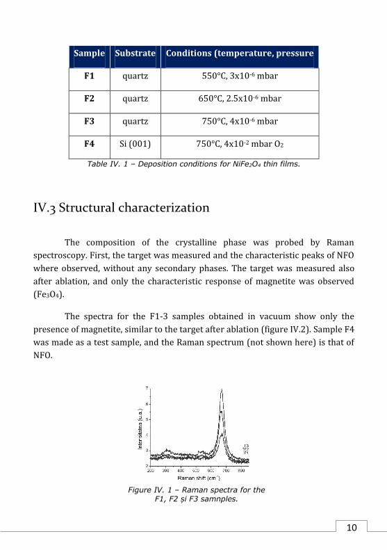
Table IV. 1 – Deposition conditions for NiFe2O4 thin films.

IV.3 Structural characterization

The composition of the crystalline phase was probed by Raman

spectroscopy. First, the target was measured and the characteristic peaks of NFO

where observed, without any secondary phases. The target was measured also

after ablation, and only the characteristic response of magnetite was observed

(Fe3O4).

The spectra for the F1-3 samples obtained in vacuum show only the

presence of magnetite, similar to the target after ablation (figure IV.2). Sample F4

was made as a test sample, and the Raman spectrum (not shown here) is that of

NFO.

Figure IV. 1 – Raman spectra for the F1, F2 și F3 samnples.

11

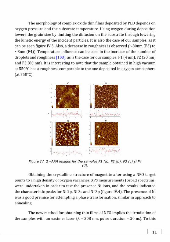
The morphology of complex oxide thin films deposited by PLD depends on

oxygen pressure and the substrate temperature. Using oxygen during deposition

lowers the grain size by limiting the diffusion on the substrate through lowering

the kinetic energy of the incident particles. It is also the case of our samples, as it

can be seen figure IV.3. Also, a decrease in roughness is observed (~80nm (F3) to

~8nm (F4)). Temperature influence can be seen in the increase of the number of

droplets and roughness [103], as is the case for our samples: F1 (4 nm), F2 (20 nm)

and F3 (80 nm). It is interesting to note that the sample obtained in high vacuum

at 550°C has a roughness comparable to the one deposited in oxygen atmosphere

(at 750°C).

Obtaining the crystalline structure of magnetite after using a NFO target

points to a high density of oxygen vacancies. XPS measurements (broad spectrum)

were undertaken in order to test the presence Ni ions, and the results indicated

the characteristic peaks for Ni 2p, Ni 3s and Ni 3p (figure IV.4). The presence of Ni

was a good premise for attempting a phase transformation, similar in approach to

annealing.

The new method for obtaining thin films of NFO implies the irradiation of

the samples with an excimer laser (λ = 308 nm, pulse duration = 20 ns). To this

Figure IV. 2 –AFM images for the samples F1 (a), F2 (b), F3 (c) și F4 (d).

12

end, we used samples obtained at 750°C (F3 type). The irradiation was done at

various frequencies (10, 25 and 50Hz), at low fluence (around 0,15 J∙cm-2) for

45000 and 90000 pulses. Table IV.2 holds the conditions for these processes.

Sample Frequency (Hz) Number of pulses (103)

F31 10 45

F32 25 45

F33 25 90

F34 50 90

Table IV. 2 – Irradiation conditions for the F3 type samples.

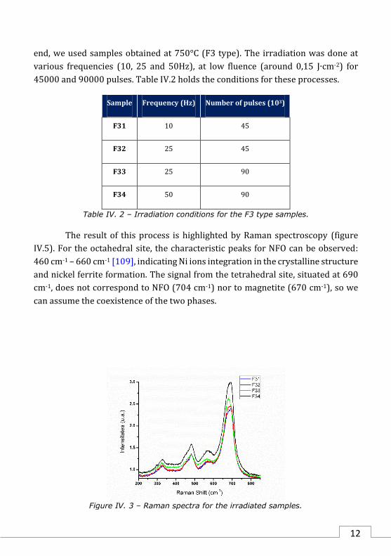
The result of this process is highlighted by Raman spectroscopy (figure

IV.5). For the octahedral site, the characteristic peaks for NFO can be observed:

460 cm-1 – 660 cm-1 [109], indicating Ni ions integration in the crystalline structure

and nickel ferrite formation. The signal from the tetrahedral site, situated at 690

cm-1, does not correspond to NFO (704 cm-1) nor to magnetite (670 cm-1), so we

can assume the coexistence of the two phases.

Figure IV. 3 – Raman spectra for the irradiated samples.

13

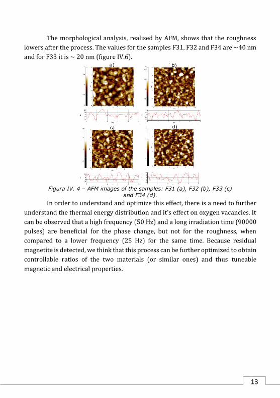
The morphological analysis, realised by AFM, shows that the roughness

lowers after the process. The values for the samples F31, F32 and F34 are ~40 nm

and for F33 it is ~ 20 nm (figure IV.6).

In order to understand and optimize this effect, there is a need to further

understand the thermal energy distribution and it’s effect on oxygen vacancies. It

can be observed that a high frequency (50 Hz) and a long irradiation time (90000

pulses) are beneficial for the phase change, but not for the roughness, when

compared to a lower frequency (25 Hz) for the same time. Because residual

magnetite is detected, we think that this process can be further optimized to obtain

controllable ratios of the two materials (or similar ones) and thus tuneable

magnetic and electrical properties.

Figura IV. 4 – AFM images of the samples: F31 (a), F32 (b), F33 (c) and F34 (d).

Chapter V. Nanostructured multiferroic system

BiFeO3 – CoFe2O4

V.1 Introduction

The present study focused on growth and characterisation and

characterization of vertical magnetoelectric heterostructures consisting of

magnetic pillars embedded in a ferroelectric matrix. We aimed at developing a

process that results in a highly ordered arrangement of the pillars. For this

purpose we chose ferrimagnetic nickel ferrite (CoFe2O4 – CFO) and ferroelectric

bismuth ferrite (BiFeO3 – BFO).

Previous studies suggested that samples obtained by self-assembly

present a certain hexagonal symmetry of the pillars in the matrix, given by

substrate mediated strain interactions [13,113,114]. Thus, initially, such a sample

was studied in order to find out the characteristic sizes of this symmetry. To this

means, we analysed the autocorrelation image of the topography, which indicates

the said symmetry, and the radially averaged autocorrelation function, from which

the mean distance to the first neighbour ensues to be 285 nm (figure V.1) [115].

V.2 Synthesis method

We used a process based on self-assembly, to which we added an initial

step of patterning the nucleation positions of the magnetic pillars, in order to

induce the desired ordering. The schematics of the process is presented in figure

V.2. The patterning was achieved using Au masks made by electron beam

lithography (EBL) on the substrates. Through these masks, CFO islands were

deposited to act as nucleation points. After the mask removal, the composite was

15

deposited from a mixed target. The mask parameters were chosen by taking into

account the analysis results of the self-assembled sample.

Before the mask transfer, SrRuO3 (SRO) was deposited on (001) oriented

SrTiO3 (STO) to act as bottom electrode. Au masks were fabricated to have to

symmetries: hexagonal and square. For both arrangements, two inter-pore

distances (pitches) have been used: 200 nm and 300 nm. The pore diameter for all

cases was kept constant at around 110 nm and the thickness at 50 nm (figure V.4).

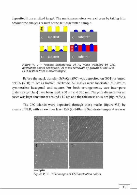
The CFO islands were deposited through these masks (figure V.5) by

means of PLD, with an excimer laser KrF (λ=248nm). Substrate temperature was

Figure V. 1 – Process schematics: a) Au mask transfer; b) CFO nucleation points deposition; c) mask removal; d) growth of the BFO-CFO system from a mixed target.

Figure V. 5 – SEM images of CFO nucleation points

16

kept constant at 600°C and oxygen pressure at 0.1 mbar. Based on deposition

parameters, the height of the islands were estimated to be maximum 10 nm. After

the deposition, the Au was chemically removed in a solution consisting 8 wt.%

iodine, 21 wt.% potassium iodide and 71 wt.% distilled water.

The last step of the process was the deposition, from a mixed target of

BFO-CFO (65%-35% molar ratio). Substrate temperature was kept at 650°C and

oxygen pressure at 0.15 mbar.

V.3 Structural characterization

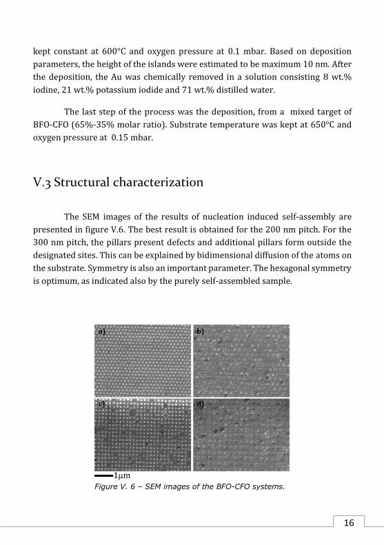
The SEM images of the results of nucleation induced self-assembly are

presented in figure V.6. The best result is obtained for the 200 nm pitch. For the

300 nm pitch, the pillars present defects and additional pillars form outside the

designated sites. This can be explained by bidimensional diffusion of the atoms on

the substrate. Symmetry is also an important parameter. The hexagonal symmetry

is optimum, as indicated also by the purely self-assembled sample.

Figure V. 6 – SEM images of the BFO-CFO systems.

17

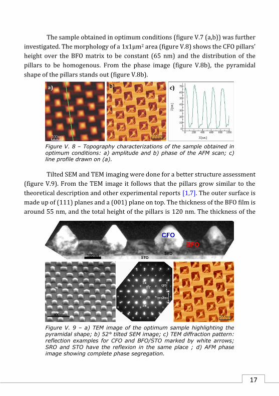
The sample obtained in optimum conditions (figure V.7 (a,b)) was further

investigated. The morphology of a 1x1µm2 area (figure V.8) shows the CFO pillars’

height over the BFO matrix to be constant (65 nm) and the distribution of the

pillars to be homogenous. From the phase image (figure V.8b), the pyramidal

shape of the pillars stands out (figure V.8b).

Tilted SEM and TEM imaging were done for a better structure assessment

(figure V.9). From the TEM image it follows that the pillars grow similar to the

theoretical description and other experimental reports [1,7]. The outer surface is

made up of (111) planes and a (001) plane on top. The thickness of the BFO film is

around 55 nm, and the total height of the pillars is 120 nm. The thickness of the

Figure V. 8 – Topography characterizations of the sample obtained in optimum conditions: a) amplitude and b) phase of the AFM scan; c) line profile drawn on (a).

Figure V. 9 – a) TEM image of the optimum sample highlighting the pyramidal shape; b) 52° tilted SEM image; c) TEM diffraction pattern: reflection examples for CFO and BFO/STO marked by white arrows; SRO and STO have the reflexion in the same place ; d) AFM phase image showing complete phase segregation.

18

bottom SRO electrode is ~20 nm. The quality of the epitaxial growth can be seen

from the diffraction pattern of the TEM, which demonstrates a cube-on-cube

epitaxy.

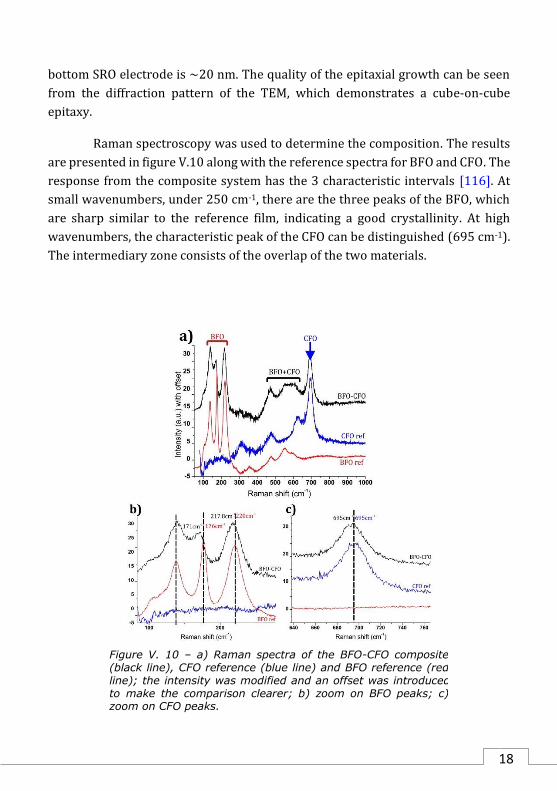
Raman spectroscopy was used to determine the composition. The results

are presented in figure V.10 along with the reference spectra for BFO and CFO. The

response from the composite system has the 3 characteristic intervals [116]. At

small wavenumbers, under 250 cm-1, there are the three peaks of the BFO, which

are sharp similar to the reference film, indicating a good crystallinity. At high

wavenumbers, the characteristic peak of the CFO can be distinguished (695 cm-1).

The intermediary zone consists of the overlap of the two materials.

Figure V. 10 – a) Raman spectra of the BFO-CFO composite (black line), CFO reference (blue line) and BFO reference (red line); the intensity was modified and an offset was introduced to make the comparison clearer; b) zoom on BFO peaks; c) zoom on CFO peaks.

19

V.4 Functional characterization

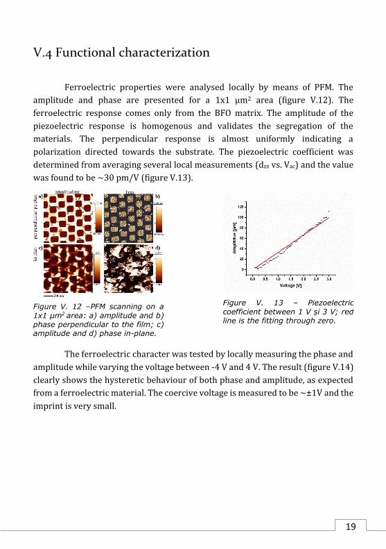
Ferroelectric properties were analysed locally by means of PFM. The

amplitude and phase are presented for a 1x1 µm2 area (figure V.12). The

ferroelectric response comes only from the BFO matrix. The amplitude of the

piezoelectric response is homogenous and validates the segregation of the

materials. The perpendicular response is almost uniformly indicating a

polarization directed towards the substrate. The piezoelectric coefficient was

determined from averaging several local measurements (dzz vs. Vac) and the value

was found to be ~30 pm/V (figure V.13).

The ferroelectric character was tested by locally measuring the phase and

amplitude while varying the voltage between -4 V and 4 V. The result (figure V.14)

clearly shows the hysteretic behaviour of both phase and amplitude, as expected

from a ferroelectric material. The coercive voltage is measured to be ~±1V and the

imprint is very small.

Figure V. 12 –PFM scanning on a 1x1 µm2

area: a) amplitude and b) phase perpendicular to the film; c) amplitude and d) phase in-plane.

Figure V. 13 – Piezoelectric coefficient between 1 V și 3 V; red line is the fitting through zero.

20

The magnetic force microscopy measurements show magnetic activity and

no preferred magnetization orientation (figure V.15). The measurements’

resolution is low, given the size of the MFM tip (radius of curvature ~70 nm), being

close to the apex of the pillars.

V.5 Magnetoelectric coupling

The magnetoelectric coupling was tested via magnetocapacitance

measurements. The parallel plate configuration was used, as shown in figure V.17.

The top electrode was manufactured out of silver paste, with a diameter of ~0.3

mm. The magnetic field was applied perpendicular to the film and it was varied in

the -80 kOe ÷ +80 kOe interval. The dc voltage applied to the sample had the

amplitude of 0.6 V. The capacitance was measured with a E4980A precision LCR

meter at four frequencies (1, 10, 100 and 1000 kHz) and four temperatures (10,

160, 200 and 260K). The assumed model was that of the parallel capacitance (C

and a loss parallel resistor). This model is valid for high impedance samples, in the

frequency interval that we used [92]. Table V.1 holds the measuring conditions.

T fVac 1kHz 10kHz 100kHz 1MHz

Figure V. 14 – Ferroelectric switching revealed through phase hysterezis curve and “butterfly-like” amplitude curve.

21

Table V. 1 – Magnetocapacitance measurements’ conditions.

For the temperature of 10K, the capacitance vs. magnetic field is presented

in figure V.18. At this temperature, one would expect the two materials to have

very low conductivity and thus very low losses, leading to precise and valid

measurements. The initial value of CP, for B=0 kOe, is in the pF range, meaning a

very high impedance. The unwanted influence of the combination of

magnetoresistance with Maxwell-Wagner effect can be ruled out by the saturation

of the magnetocapacitance and it’s little variation with frequency. At high

frequencies (1MHz), a certain change in behaviour and value can be observed. This

can be attributed to the effect of the contacts series resistance. All measurements

show an interval of quadratic dependence on the field (±25 kOe), and two linear

intervals of similar slope.

10K

𝐵 𝜖 (−80 𝑘𝑂𝑒, +80 𝑘𝑂𝑒)

|𝑉𝑎𝑐| = 0.6 𝑉

160K

200K

260K

Figura V. 17 – Magnetocapacitance measurement system.

22

The direct magnetoelectric effect implies the appearance of an electrical

polarization when a magnetic field is applied. The magnetoelectric coupling

coefficient can be related to the change in capacitance as follows:

𝛼 ∙ 𝐻 = ∆𝐶(𝐻) ∙𝑉

𝐴

Thus, the value of the coefficient can be determined from the slope of the

magnetocapacitance variation. Using the two straight zones, the value of the

coefficient was found to be ~0.6 and ~0.9 𝜇𝐶/𝑐𝑚 ∙ 𝑂𝑒, respectively (figure V.19).

To validate the results and rule out any unwanted influences, the losses

and their change in magnetic field have to be taken into account (figure V.20). At 1

kHz and 10 kHz, the losses are low and they do not vary more then 1.5%. At higher

frequencies (100kHz and 1MHz), the losses are higher and their dependency in

magnetic field is more clearly outlined as being hysteretic.

Figure V. 18 – Capacitance vs. magnetic field (absolute and relative values) at 10K.

23

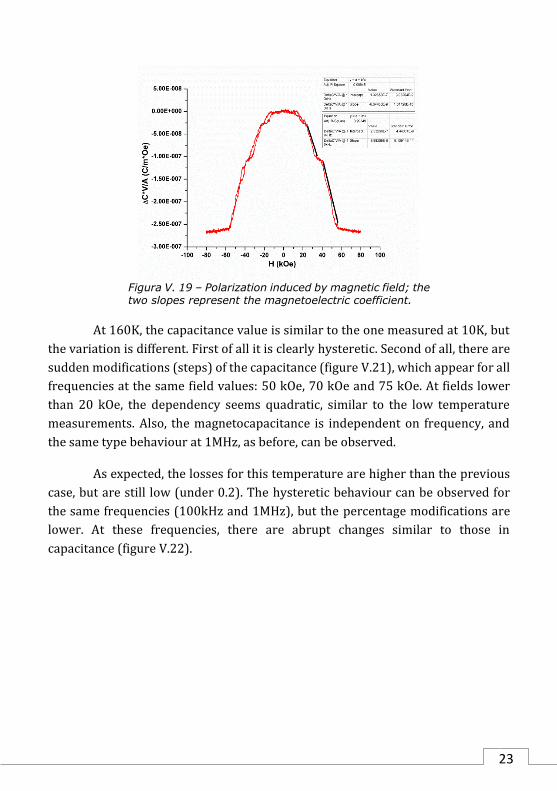
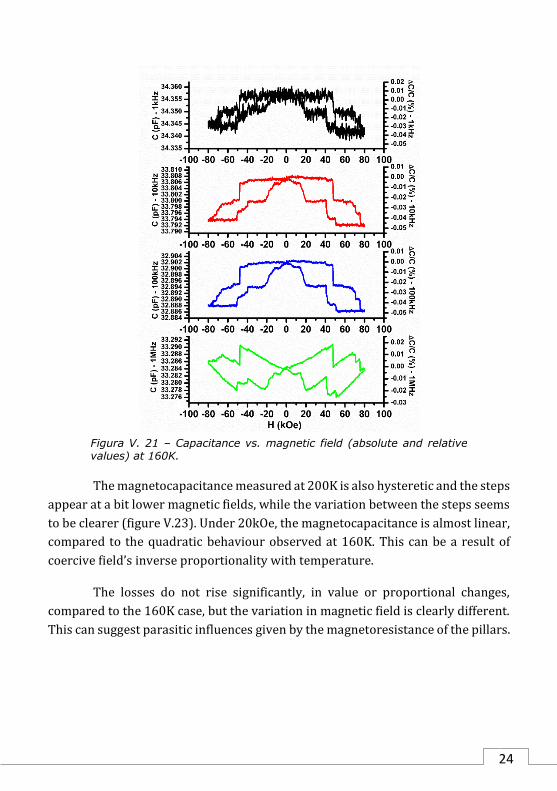
At 160K, the capacitance value is similar to the one measured at 10K, but

the variation is different. First of all it is clearly hysteretic. Second of all, there are

sudden modifications (steps) of the capacitance (figure V.21), which appear for all

frequencies at the same field values: 50 kOe, 70 kOe and 75 kOe. At fields lower

than 20 kOe, the dependency seems quadratic, similar to the low temperature

measurements. Also, the magnetocapacitance is independent on frequency, and

the same type behaviour at 1MHz, as before, can be observed.

As expected, the losses for this temperature are higher than the previous

case, but are still low (under 0.2). The hysteretic behaviour can be observed for

the same frequencies (100kHz and 1MHz), but the percentage modifications are

lower. At these frequencies, there are abrupt changes similar to those in

capacitance (figure V.22).

Figura V. 19 – Polarization induced by magnetic field; the two slopes represent the magnetoelectric coefficient.

24

The magnetocapacitance measured at 200K is also hysteretic and the steps

appear at a bit lower magnetic fields, while the variation between the steps seems

to be clearer (figure V.23). Under 20kOe, the magnetocapacitance is almost linear,

compared to the quadratic behaviour observed at 160K. This can be a result of

coercive field’s inverse proportionality with temperature.

The losses do not rise significantly, in value or proportional changes,

compared to the 160K case, but the variation in magnetic field is clearly different.

This can suggest parasitic influences given by the magnetoresistance of the pillars.

Figura V. 21 – Capacitance vs. magnetic field (absolute and relative values) at 160K.

Figura V. 23 – Capacitance vs. magnetic field (absolute and relative values) at 200K.

Conclusions

The present study led to the development of a synthesis method for highly

ordered vertical magnetoelectric heterostructures, based on PLD and self-

assembly. Using Au masks for the deposition of the pillars’ nucleation points,

several arrangements, of different symmetries and parameters, were obtained.

The subsequent deposition was done from a mixed target, similar to the self-

assembly process. The structural characterisations show the success of the

nucleation-induced self-assembly process. The optimum conditions involve a

hexagonal symmetry with a mask inter-pore distance of 150 nm.

The functional investigations reveal ferroelectric properties of the BFO

matrix to be similar to thin films, with low coercive voltage, small imprint and high

piezoelectric coefficient. Local magnetic measurements show magnetic activity,

but the low resolution doesn’t allow to clearly differentiate between the magnetic

domains in a pillar.

Magnetoelectric coupling is shown at various temperatures by means of

magnetocapacitance measurements. The validity of the results is supported by the

small value of losses and the small influence of frequency.

An additional study on nickel ferrite thin films revealed a new process for

the synthesis of nickel ferrite thin films by laser irradiation of magnetite films with

nickel inclusions. Compositional analysis shows the presence of both NFO and

magnetite in the resulting samples. The influence of several parameters on

morphology is shown.

Selective bibliography

[5] P. Curie, J. Physique, 1894, 3, 393.

[6] P. Debye, Z. Phys., 1926, 36, 300.

[7] L. D. Landau and E. M. Lifshitz, Electrodynamics of continuous media (Fizmatgiz,

Moscow, 1959).

[8] I. E. Dzyaloshinskii, Sov. Phys. – JETP, 1959, 10, 628.

[9] D. Astrov, Sov. Phys. – JETP, 1960, 11, 708.

[10] I.F. Martinez, Ferroelectricity and magnetoelectric coupling in magnetic

ferroelectrics and artificial multiferroic heterostructures, (Barcelona, 2012).

[11] N. A. Hill, The Journal of Physical Chemistry B, 2000, 104, 6694.

[12] J. Wang, J. B. Neaton, H. Zheng, V. Nagarajan, S. B. Ogale, B. Liu, D. Viehland, V.

Vaithyanathan, D. G. Schlom, U. V. Waghmare, N. A. Spaldin, K. M. Rabe, M. Wuttig, and R.

Ramesh, Science, 2003, 299, 1719.

[13] H. Zheng, J.Wang, S. E. Lofland, Z. Ma, L. Mohaddes-Ardabili, T. Zhao, L. Salamanca-

Riba, S. R. Shinde, S. B. Ogale, F. Bai, D. Viehland, Y. Jia, D. G. Schlom, M. Wuttig, A. Roytburd,

and R. Ramesh, Science, 2004, 303, 661.

[14] B.D.H. Tellegen, Philips Res. Rep., 1948, 3, 81.

[15] J. van Suchtelen, Philips Res. Rep., 1972, 27, 28.

[39] M. Fiebig, T. Lottermoser, D. Frohlich, A.V. Goltsev, and R.V. Pisarev, Nature, 2002,

419, 818.

[40] Y.-H. Chu, L.W. Martin, M.B. Holcomb, M. Gajek, S.-J. Han, Q. He, N. Balke, C.-H. Yang,

D. Lee, W. Hu, Q. Zhan, P.-L. Yang, A. Fraile-Rodríguez, A. Scholl, S. X. Wang and R. Ramesh,

Nature Materials, 2008, 7, 478.

[43] L. Mitoseriu and V. Buscaglia, Phase Transitions, 2006, 79, 1095.

[44] G. Harshe, J.P. Dougherty and R.E. Newnham, Proc. SPIE, 1973, 1919, 224.

[53] F. Zavaliche, H. Zheng, L. Mohaddes-Ardabili, S. Y. Yang, Q. Zhan, P. Shafer, E. Reilly,

R. Chopdekar, Y. Jia, P. Wright, D. G. Schlom, Y. Suzuki and R. Ramesh, Nano Letters, 2005, 5,

1793.

28

[60] V.M. Goldschmidt, Naturwissenschaften, 1926, 14, 477.

[62] G. Catalan, J. Scott, Advanced Materials, 2009, 21, 2463–2485.

[66] J. Li, J. Wang,M.Wuttig, R. Ramesh, N. Wang, B. Ruette, A. P. Pyatakov, A. K. Zvezdin,

D. Viehland, Appl. Phys. Lett., 2004, 84, 5261.

[70] F. Johann, A. Morelli, D. Biggemann, M. Arredondo, I. Vrejoiu, Physical Review B,

2011, 84, 1–10.

[78] J.F. Scott, Journal of Materials Chemistry, 2012, 22, 4567.

[79] Robert Eason, Pulsed Laser Deposition of Thin Films – Applications-led Growth of

Functional Materials (Ed. Wiley, 2007).

[86] R.N. Rodin and D. Walter, Single crystal films, (ed. Francombe, H. Maurice and H.

Sato, Pergamon Press, N.Y. 1964).

[88] Alessio Morelli, Piezoresponse Force Microscopy of Ferroelectric Thin Films

(University of Groningen, Zernike Institute OhD thesis series 2009-12, 2009).

[89] Weilie Zhou, Zhong Lin Wang, Scanning Microscopy for Nanotechnology Techniques

and Applications (Springer Science+Business Media, LLC, 2006).

[90] G. Catalan, Applied Physics Letters, 2006, 88, 102902.

[92] Agilent, Agilent Impedance Measurement Handbook (edited by I. Agilent

Technologies, Agilent Technologies, Inc., 2009).

[96] Peter Larkin, Infrared And Raman Spectroscopy Principles And Spectral

Interpretation (Elsevier Inc., 2011).

[110] H. Zheng, F. Straub, Q. Zhan, P.-L. Yang, W.-K. Hsieh, F. Zavaliche, Y.-H. Chu, U.

Dahmen, R. Ramesh, Advanced Materials, 2006, 18, 2747–2752.

[111] H. Zheng, J. Wang, L. Mohaddes-Ardabili, M. Wuttig, L. Salamanca-Riba, D.G.

Schlom, R. Ramesh, Applied Physics Letters, 2004, 85, 2035.

[112] R. Comes, H. Liu, M. Khokhlov, R. Kasica, Nano Letters, 2012.

[113] M. Dawber, I. Szafraniak, M. Alexe, J.F. Scott, Journal of Physics: Condensed Matter,

2003, 15, L667–L671.

[114] J. Slutsker, Z. Tan, A. Roytburd, I. Levin, J. Mater. Res., 2007, 22, 2087–2095.

[117] F. Johann, A. Morelli, D. Biggemann, M. Arredondo, I. Vrejoiu, Physical Review

B,2011, 84, 1–10.

Communications and publications list:

1. „Alternative route for obtaining NiFe2O4 by PLD”, Sergiu M Stratulat, Cristian Ursu,

Ovidiu Florin Călțun, 9th European Conference on Magnetic Sensors and

Actuators, 1-4 Iulie 2012, Praga, Cehia; tipul comunicării: poster;

2. „Nucleation-induced self-assembly of nanostructured BiFeO3-CoFe2O4”, Sergiu M

Stratulat, Dietrich Hesse, Marin Alexe, Deutsche Physikalische Gesellschaft, 10-

15 Martie 2013, Regensburg, Germania; tipul comunicării: prezentare orală;

3. „Nucleation-induced self-assembly of nanostructured BiFeO3-CoFe2O4”, Sergiu M

Stratulat, Dietrich Hesse, Marin Alexe, WG1 Workshop “Nanoscale phenomena”

& Core Group meeting, 18-22 Martie 2013, Belfast, U.K.; tipul comunicării:

prezentare orală;

„Alternative route for obtaining NiFe2O4 by PLD”, Sergiu M Stratulat, Cristian Ursu,

Ovidiu Florin Călțun, IEEE Transactions on Magnetics, vol. 49, no. 1, january

2013.

„Nucleation-Induced Self-Assembly of Multiferroic BiFeO3−CoFe2O4 Nanocomposites”, Sergiu

M. Stratulat, Xiaoli Lu, Alessio Morelli, Dietrich Hesse, Wilfried Erfurth, and Marin Alexe,

Nano Letters, 2013, dx.doi.org/10.1021/nl401965z.


Recommended