80

2
o Tin Whisker Mitigationo PCB Surface Finish Selectiono Solder Alloys – What to use?o Manufacturing Defects
o Head-in-pillowo Improper reflow & Rework
What are the primary Pb-Free Concerns and how
are they being addressed?

3
Risk of Tin Whiskers

4
Tin Whiskers
o Tin whiskers are hair-like single crystal metallic filaments that grow from tin films.
o Their unpredictability is the greatest concern.
o The Aerospace and Defense industries consider tin whiskers the, “greatest reliability risk associated with Pb-free electronics”.
o Manhattan project phase 2 report

55
What are the potential failure modes?o Direct Contact
o Causes an electrical short (arcing)
o Requires growth of sufficient length and in the correct orientation
o Electromagnetic (EM) Radiation
o Emits or receives EM signal and noise at higher frequencies
o Deterioration of signal for frequencies above 6 GHz independent of whisker length
o Debris
o Whisker breaks off and shorts two leads (primarily during handling)
Courtesy of P. Bush, SUNY Buffalo
Observation of tin whisker debris as
reported to NASA from Sanmina-SC
DfR Solutions
5

6
Where have tin whiskers caused failures?o Bright Tin on the case of a pacemaker crystal component
(in 1986).

7
Where have tin whiskers caused failure?o Satellites
o Whisker growth and subsequent short results in a low pressure arc in vacuum (vaporized tin creates a plasma).
o Don’t use Sn plating in satellite applications (risk may be low but the cost of failure is very high).

8
What drives tin whisker growth? Sn whiskers occur on tin primarily due
to compressive stress which can be caused by:
o Stress during plating of Sno Intermetallic formation with Cuo Mechanical or CTE mismatch stress
Cu6Sn5 requires
more volume than
independent Cu & Sn
Without Compressive stress in tin whiskers do not form

9
Eliminate the Compressive Stress in tin to Mitigate Whisker Growth.
The stresses that drive whiskering primarily derive from five sources.
o Base metal (intermetallic formation)
o Base metal (differences in coefficient of thermal expansion)
o Bulk plating properties
o Oxidation/Corrosion
o External pressure
Mitigation

10
o The formation of Cu6Sn5 creates a volume expansion at the grain boundaries.
o Cu diffusion occurs faster along the Sn grain boundaries, so this is where the most IMC forms.
o This is the most common cause of compressive stress that produces tin whiskers.
Cu Base Metal (Intermetallic Formation)

11
o Use of Ni as an underplate is a common method to prevent interdiffusion of the tin and copper and thus formation of Cu6Sn5.
o The resulting Sn3Ni4 is relatively thin and uniform due to the low dissolution rate of Ni in Sn compared to Cu.
o A slight tensile stress is created with this IMC.
Mitigation – Ni Barrier
Ni Underplate (> 1.27 micrometers)

12
o When Ni underplate is not practical (a formed leadframefor instance) then annealing is often used as a whisker mitigation.
o Heating the tin coating to 150-170 C for 30-60 min immediately after plating forces the formation of Cu3Sn intermetallic (thermodynamically stable at temperatures over 60C).
o This IMC does not induce compressive stress and provides a uniform layer that reduces the rate of additional copper diffusion into the tin.
o Similar, but not as effective, as the Ni underlayer.
Mitigation - Annealing

13
o Compressive stress can also arise when the base metal has a lower coefficient of thermal expansion (CTE) than tin plating and the component is subjected to repeated changes in temperature.
o Best mitigation is to avoid components with tin plating on alloy 42, steel, or bronze, where whiskers can grow very long.
Thermal Expansion Stress

14
o Matte tin is dull looking because it consists of large grains and an uneven surface.
o For improved aesthetics carbon brighteners are added to the plating bath; these essentially provide nucleation sites for new grains to grow.
o The result is a tin plating with small grain size and a smoother brighter surface.
Brighteners

15
o D-Sub Connectors with bright tin shells have been known to grow whiskers that can short our pins (if connector is unmated).
Bright Tin Whisker Examples
Whiskers also found to grow in screw holes.
Ref: L. Flasche & T. Munsun, Foresite, Inc. 9/09.
Ref: Emerson

161616
When Do Really Long Whiskers Occur?� Usually bright tin and/or tin plating over a substrate
material other than copper (brass or steel)
NASA (Leidecker): 25 mm over +10 years DfR (Fischer): +2 mm over 6 months
Bright tin over BeCu(?) or steel(?) Tin (matte?) over brass

17
o Just as with IMC formation, the process of tin oxidation/corrosion can also induce compressive stress.
o Oxygen diffusion will occur fastest along the grain boundaries.
o The volumetric expansion can result in large compressive stresses within the plating.
o A similar situation occurs with various corrosion products.
Oxidation/Corrosion

18
o Various tin plated components soldered to the board were exposed to different levels of contamination/corrosion.
o SAC305 assemblies cleaned – showed no whisker growth
o As-received assembles (noncleaned) – showed some small whiskers (hillocks).
o Assemblies intentionally contaminated with NaCl or Na2SO4 – showed more components with long whiskers.
Corrosion Testing
QFP44, contaminated with NaCl
Ref: P. Snugovsky et. al, “Influence of Board and Component cleanliness on Whisker Formation”, BAE & Celestica, IPC & SMTA conference, 2010.

19
o Extrinsic forces can also introduce compressive stress in the tin plating.
o One of the first studies of tin whiskers was triggered by the finding that tin plated steel ring clamps grew long whiskers that depended on the clamp pressure.
o The larger the stress the longer the whiskers must grow to relieve it.
o Common pressure points in electronics include connectors, standoffs, card guides, washers/terminals, shielding, etc.
o Of particular concern is the contact pressure on flexible circuit cables.
External Pressure

20
Contact Pressure on Flex Cables
o Flex Circuits with Connector Mating
o Pressure from contacts with the soft polymer substrate creates force over a large area of tin.
o Don’t use Sn plating in mated flex with a spacing less than 200 micrometers.
o Use gold plating under such conditions.

21
o Consider the environment of the product and the cost of failure.
o Perform BOM scrub to ensure fine pitch tin plated components have Ni under plate or heat anneal
o Ensure fine pitch flex circuits are gold plated.
o Ensure bright tin is not used (and if so, a Ni under plate is used).
o Don’t use Sn over brass or steel (Ni under plate will help)
o If going into a corrosive environment, use cleaning of flux residue.
o If a lot of thermal cycling is expected, avoid alloy 42 lead-frames.
o Use conformal coating if practical.
An Overall Mitigation Approach

22
How to Select a PCB Surface Finish for LF Products?

23
Importance of SF
o The selection of the surface finish to be used on your PCBs could be the most important material decision made for the electronic assembly.
o The surface finish influences the process yield, the amount of rework necessary, field failure rate, the ability to test, the scrap rate, and of course the cost.
o One can be lead astray by selecting the lowest cost surface finish only to find that the total cost is much higher.
o The selection of a surface finish should be done with a holistic approach that considers all important aspects of the assembly.

24
What is your SF selection approach?
o Component Procurement: Select the cheapest one and let the engineers figure out how to use it.
o PCB Engineer: Select the finish that is easiest for the suppliers to provide (their sweet spot); let the assembler figure out how to use it.
o Assembly Engineer: Select the finish that provides the largest process window for assembly and test.
o Sustaining Engineer: Select the finish that minimizes field failures.
o CEO: Select the finish that minimizes the overall cost (including reliability risk).

25
Considerations with SF Selection
o Cost sensitivity
o Volume of product (finish availability)
o SnPb or LF process
o Shock/Drop a concern?
o High yield ICT is important
o Is direct wire bonding required?
o User environment (corrosion a concern)?
o Fine pitch assembly (<0.5 mm)
o Wave solder required (PCB > 0.062”)
o Are cosmetics of the PCB a concern?

26
Market Share

27
o Immersion Ag became popular with the Pb-free transition, but has concerns with creep corrosion.
o MacDermid is proposing the use of an electroless Ni immersion silver ENIS coating (to prevent access to the Cu).
o OMGI is proposing the use of electroless Pd (directly on Copper).
o Semblant is developing an organic plasma coating.
o ENEPIG is becoming more popular (to replace ENIG)
o Better for wire bonding
o Reduce risk for black pad
o ENEPES – NiPdSilver (silver replaces the Au) - Uyemura
What is new with PCB Surface Finishes?

28
o Organic film covering the Cu that breaks down with the soldering process.
o Primary challenges are probe testing through it and oxidation of underlying Cu after repeated oven passes.
Organic Solderability Preservative
Cu
OSP

29
o Thin coating of silver directly on the Cu (10-15 u”)
o Creep corrosion is the formation of copper sulfide that causes failure by bridging conductors.
o It occurs in the presence of high levels of sulfur (gas or particulate).
Immersion Silver (ImAg)

30 30
Creep Corrosion Mechanism
o Cross-section image of soldermask defined edge. Copper is attacked to form Cu2S.

31
o Don’t use ImAg (use an alternative finish)o ImSn, LF HASL, or OSP
o If you do use ImAg, use an enclosure that limits direct airflow.
o Plug vias with soldermask.
o Use conformal coatings (but not silicone which absorbs high levels of sulfur).
o Try ENIS (electroless Ni Immersion Silver)?o A layer of Ni is under the silver to reduce the chance of
exposed Cu that leads to creep corrosion.
o New to market so inherent risk involved.
How do I avoid Creep Corrosion?

3232
Immersion Sn (ImSn)
o A single material systemo Specified by IPC-4554
o Standard thickness: 1 micron (40 microinches)
o Some companies spec up to 1.5 microns (65 microinches)
o Benefitso Excellent flatness, low cost
o Not as popular a choice with PCB fabricators. o Environmental and health concerns regarding thiourea
(a known carcinogen)
o Some concern regarding tin whiskering (minimal)
o Assembly temperatures can convert tin into intermetallic and reduce solderabilty

33
o Board is fluxed and dipped into solder and cleaned.
o SnCuNi alloys work better than SAC305
Lead-Free Hot Air Solder Level
SnCuNiGe Alloy

3434
Electroless Ni Immersion Au (ENIG)
� Solder dissolves the Au and bonds to the underlying Ni.
� SAC305 solder forms a brittle intermetallic with Ni (a problem with shock/drop).
� Black pad is a potential reliability concern.� Au bath attacks and removes Ni but
leaves behind phosphorus (Electroless Ni contains 8-12%P)
� Too much attack causes the phosphorus layer to become thick and weakens the solder joint.
.
Images of Black Pad
Phosphorus-Rich Dark Streak

3535
ENIG - Ni Interface shows weakness
This is a x-section of an as-assembled PCBA (prior to testing).

36
Electroless Ni – Electroless Pd –Immersion Au
o Addition of the electrolesspalladium layer provides two primary advantages.
1. It prevents black pad (since gold bath doesn’t come in contact with Ni).
2. It enhances the wire bondability of the finish (reduces Ni diffusion through the gold)
What is ENEPIG?
Ni
Pd
Au

37
Plasma Coated Finish - Semblant
o Coated in plasma chamber.
o Many panels coated simultaneously.
o Film is 60 nm thick (easy to probe through)
o Flux breaks through film at elevated temperature (does not break down with heat).
o Hydrophobic and acid resistant
o Prevents creep corrosion600nm

38
o Low cost and simple assembly > OSP
o Low cost and will be in an enclosure with limited airflow > ImAg.
o Low cost and will see airflow > ImSn or LF HASL
o Higher cost and more difficult assembly > ENEPIG (if drop/shock is a concern, high risk components can be underfilled)
o The newer finishes could be explored as cost reductions or reliability enhancements
Brief Decision List

39
What is new with Pb-Free Solder Alloys?

40
o SAC305 is still the default Pb-free alloy
o SAC105 is being used for solder balls on BGAs in hand held devices.
o Improved shock resistance
o Worse temperature cycling results
o SnCuNi (SN100C) is now being used for surface mount (has gained much ground with wave solder).
o SnAgBi alloys being more seriously considered now that Pb has been largely purged from commercial electronics.
o Other dopants being considered for improved shock performance.
o Sn3.5%Ag solder balls being used on NiAu surfaces.
What is new with Pb-Free Alloys?

41
SAC305 is sensitive to high stress/strain fatigue.
o Solder joint fatigue life for a 2512 Resistor
Vibration Strain = 2400µϵSnPb better than SAC
Vibration Strain = 1200µϵSAC better than SnPb
Low Cycle Fatigue High Cycle Fatigue

4242
Why the difference?
o Stiffness (SAC > SnPb)
o For a given force / load, a stiffer solder will respond with a lower displacement / strain (elastic and plastic)
o Low-cycle fatigue (plasticity driven)
o Under displacement-driven mechanical cycling, lower stiffness solder will tend to out-perform higher stiffness
o High-cycle fatigue (elasticity driven)
o Under small load-driven mechanical cycling, higher stiffness solder will tend to out-perform lower stiffness
o The SAC305 solder remains in elastic state with little/no deformation and damage.

43
What about thermal cycle impact?
o If high stress is created during thermal cycle then SnPb performs better (stiffer component or larger delta T).
Ref: E. Al-Momanl and M. Mellunas, “Lead-free Thermal Cycle Progress, Unovis, June, 2008.
Flex BGACompliant Component – SAC is better
Flip Chip (no underfill)Stiff Component – SnPb is better

444444
Thermal Cycling: SnPb-SAC Transition
I. Kim, ECTC 2007
Large delta T favors SnPb solder

45
Drop Results for various Pb-Free Solders
W. Liu, N. Lee, “NOVEL SACX SOLDERS WITH SUPERIOR DROP TEST PERFORMANCE”, SMTA Proceedings, Chicago, 2006.
Indium is focusing development efforts on these.

46
Drop Testing
o 244 I/O BGA, 0.5 mm
o Electrolytic NiAu on package substrate.
o OSP on PCB.
o JEDEC Drop Test method used.
o 250 thermal cycles precondition
Ref: W. Liu et al., “Achieving High Reliability Low Cost LF SAC Solder Joints via Mn or Ce Doping”, ECTC, 2009.

47
o Sn-1.0Ag-0.1Cu-0.02Ni-0.05In
o Sn-1.0Ag-0.7Cu-0.1Ge
o Sn-1.2Ag-0.5Cu-0.05Ni
o Sn2.5Ag-0.8Cu-0.5Sb
o Sn-0.3Ag,-0.7Cu-Bi+X (SAC0307)
o Alloys containing Bi are more prevalent as well
Other alloys with Favorable Drop Performance

48
o Stick with SAC305 until other alloys have been fully investigated and implemented.
o SnCuNi Alloy is getting more use as a surface mount alloy – so this is becoming another viable option.
o Deal with the known weaknesses through good manufacturing processes and engineering solutions
o Limit board strain
o Reinforce weak components
Overall Opinion on LF Alloy Selection

49
o DfR Solutions has developed a sophisticated modeling program that will perform an analysis of a completed circuit board assembly.
o Expected environmental conditions are input and the resulting solder joint reliability expectations are produced.
o Thermal cycle
o Vibration
o Shock
o Comparisons can be made between SnPb and SAC305 solder (or other alloys).
Modeling of SAC305 Solder Joints

50
Comparison of SnPb to SAC305 - Example
Assume:
o Eutectic SnPb
o -40C to 101C
o 1 cycle per day
Assume:
o SAC305
o -40C to 101C
o 1 cycle per day
51
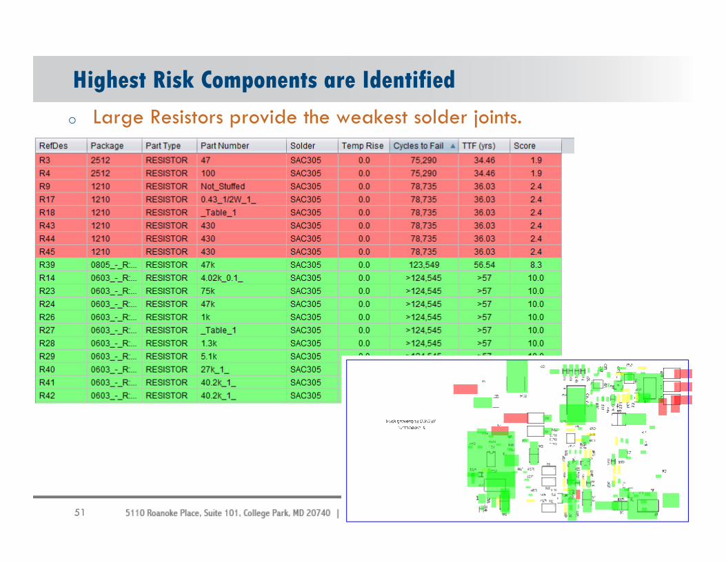
Highest Risk Components are Identified
o Large Resistors provide the weakest solder joints.

52
Harmonic Vibration Results - Example
Board level strains during vibration exposure

53
Vibration Results – Component Breakdown

54
Common Pb-Free Manufacturing Defects

55
o Cracked laminate (pad cratering)
o Head-in-pillow
o Inadequate hole fill (wave solder)
o Cu Dissolution
o Heat damaged PCB or components.
o Poor rework (insufficient thermal profile)
What are the most common manufacturing
defects with Pb-free?
56
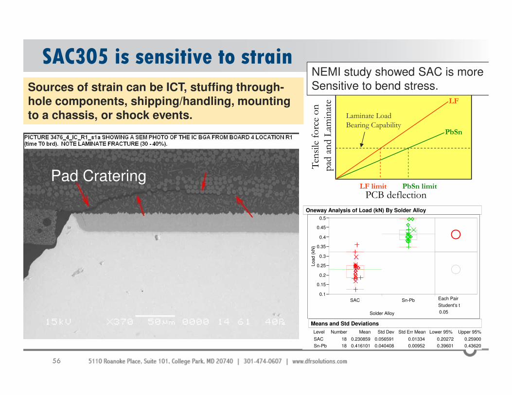
SAC305 is sensitive to strain
PCB deflection
Tensile force on
pad and Laminate
PbSn
LF
PbSn limitLF limit
Laminate Load
Bearing Capability
Load (
kN
)
0.1
0.15
0.2
0.25
0.3
0.35
0.4
0.45
0.5
SAC Sn-Pb
Solder Alloy
Each Pair
Student's t
0.05
SAC
Sn-Pb
Level
18
18
Number
0.230859
0.416101
Mean
0.056591
0.040408
Std Dev
0.01334
0.00952
Std Err Mean
0.20272
0.39601
Lower 95%
0.25900
0.43620
Upper 95%
Means and Std Deviations
Oneway Analysis of Load (kN) By Solder Alloy
NEMI study showed SAC is moreSensitive to bend stress.Sources of strain can be ICT, stuffing through-
hole components, shipping/handling, mounting
to a chassis, or shock events.
Pad Cratering

57
BGA
Too Little Too MuchCorrect
Target approximately 50% of BGA substrate height
Edge Bonding is effective at reducing pad cratering.
To be most effective, length of bead should be 4-6 solder balls in length.
Ref: M. Kochenowski et. al., Improved Shock and Bend with Corner Glue, SMTA, Chicago, 2006.

58
Corner Glue – Results
Post-Reflow Glue Failure mech
Ref: M. Kochenowski et. al., Improved Shock and Bend with Corner Glue, SMTA, Chicago, 2006.

59
o Use dummy pads in corners of BGA (solder mask defined)
o Use laminates that are more resistant to cracking
o Dicy vs. Phenolic
o Prevent board deflection in manufacturing
o Use well placed mount points that limit bending at corners of large BGAs
o If all else fails – corner staking or underfill
Pad Cratering Prevention

60
Head-in-Pillow Defectso Head-in-pillow (HnP) joints are not a new defect mode with Pb-
free, however since assembly with SAC solder began, this defect mode has become significantly more prevalent (many field failures are being reported).
o A HnP joint will pass X-ray inspection, in-circuit testing, and functional testing.
o Failures occur in the field after large volumes of products have been shipped (worst case situation).

61
X-ray can now detect HnP
o 3D X-ray with Computerized Tomography (CT) can detect HnP defects.
2D Image 3D CT Image
Nordson Dage Precision

62
Optical Inspection Scopes

63
Two Types of HnP Causes
1. Poor Wetting
o Tends to be isolated and randomly located
2. Warpage Induced
o Usually occurs at corners and edges with multiple opens.
M. Scalzo, “Addressing Issues of Head-in-pillow Defects”, IPC Midwest, Chicago, Sept., 2010.
64
What is the Root Cause mechanism?
o HnP occurs when the flux on the exterior of the paste dries out prior to reaching liquidus temperature.
o In the case of warping, the paste and ball are not in contact at liquidus and come back together upon cooling.
o Result is oxidized surfaces that prevent intermixing.
o The higher temperatures required for lead-free assembly exacerbates both causes.

65
Mechanism for HnP and Non-Wet Open (NWO)
D. Amir, et.al, “The Challenges of Non-Wet Open BGA Solder Defect”, SMTA Int’l Conference, Orlando, FL, 2012.

66
What variables impact HnP?
o Supplier Issues:
o Flux activity, slump resistance, tackiness.
o Sphere oxidation
o IC package Warpage
o PCB Warpage
o Process Issues
o Poor paste printing (insufficient volume).
o Component placement (insufficient pressure, off pad).
o Reflow
o Too much time in preheat.
o Insufficient time above liquidus (TAL).

67
What are best prevention practices?
o Intel has performed DoEs to show impact of some variables.
o Increasing TAL reduces HnP, however, us of N2
in reflow eliminates the defect altogether o Nitrogen flow should ensure the oxygen level is < than 3000
ppm.
Reference: Intel design guide Nov. 2008

68
Prevention Practices – Paste Volume
o Increasing the paste volume can also be beneficial (by increasing stencil opening or thickness).

69
Other preventative actions?
o Press component down in the solder paste.
o Dip the component balls into a tacky flux prior to placing into the paste.
o Run a linear reflow profile (no constant temp soak).
o Solder suppliers are working on paste/flux with improved capabilities.
o Process optimization is critical (not just using the first conditions that seem to work).

70
IPC-A-610D Hole Fill Requirements
These specs can be very difficult to achieve with certain Pb-free material combinations.

71
Hole Fill Challenges with SAC and SnCu
Less than50% hole fill
To achieve sufficient hole-fill suppliers often increase the preheat temp,
solder pot temp and dwell time (this can damage other components).
Must optimize surface finish and wave solder alloy for your application.

727272
Solders: Copper Dissolution with SAC
o PTH knee is the point of greatest plating reduction
o Primarily a rework/repair issue
o Celestica identified significant risk with >1X rework
o Dissolution on BGAs can also be an issue (when Ni barrier not used).
S. Zweigart, Solectron
Sn100C in wave solder has largely alleviated this issue

73
o Rework is perhaps one of the most significant challenges.
o Process window required is small
o Too cool results in poor or incomplete solder joints.
o Too hot results in damaging the component, the PCB, or neighboring components.
o The window can be consistently hit with a dialed in 9+ zone oven, but small scale rework stations are difficult.
o Rework operators tend to be less experienced and the processes less documented/controlled.
o Trial and error tends to be used.
Pb-Free Rework

74 Page 74
Pb-Free Rework Issues
CPU Socket with insufficient reflow

75
Examples of Pb-Free IssuesBGA Rework Defects

76Pa
Pb-Free Rework IssuesOverheating of CPU socket during rework. Cu pad nearly all converted to intermetallic.
Resolved by better control of rework process. In some cases suppliers purchased newer equipment for better temp uniformity.

77
LF Rework – board damage
Need to look for
more than just solder joint defects from overheating

78
Rework Damage (to PCB or surrounding components)

79
Summary
o Tin whiskers are a risk but can be significantly mitigated with awareness and precautions.
o High strain rate failure of SAC305 solder joints require careful material handling, design, and in some cases reinforcement of components.
o Select and optimize material sets (laminates, solders, surface finishes).
o Be aware of the various manufacturing defects and inspect for them.
o Head-in-pillow defects must be addressed in the material specification and assembly process.
o Rework profiles must be well documented and controlled (process window is much smaller than with SnPb)


