Blending of n‑type Semiconducting Polymer and PC61BM for anEfficient Electron-Selective Material to Boost the Performance of thePlanar Perovskite Solar CellYou-Hyun Seo,†,∥ Jun-Seok Yeo,‡,⊥,∥ NoSoung Myoung,§ Sang-Youp Yim,§ Minji Kang,‡ Dong-Yu Kim,‡
and Seok-In Na*,†
†Professional Graduate School of Flexible and Printable Electronics and Polymer Materials Fusion Research Center, ChonbukNational University, Jeonju-si, Jeollabuk-do 561-756, Republic of Korea‡School of Materials Science and Engineering and §Advanced Photonics Research Institute (APRI), Gwangju Institute of Science andTechnology, Gwangju 500-712, Republic of Korea
*S Supporting Information
ABSTRACT: The highly efficient CH3NH3PbI3 perovskite solar cell(PeSC) is simply achieved by employing a blended electron-transportlayer (ETL) consisting of PC61BM and P(NDI2OD-T2). The highmolecular weight of P(NDI2OD-T2) allows for a thinned ETL with auniform morphology that optimizes the PC61BM ETL more effectively.As a result of this enhancement, the power conversion efficiency of aPC61BM:P(NDI2OD-T2)-based PeSC is 25% greater than that of theconventional PC61BM based-PeSC; additionally, the incorporation ofP(NDI2OD-T2) into PC61BM attenuates the dependence of the PeSCon the ETL-processing conditions regarding its performance. It isrevealed that, in addition to the desirable n-type semiconductingcharacteristics of PC61BM:P(NDI2OD-T2)including a higher elec-tron-mobility and a more-effective electron selectivity of a blended ETLfor an efficient electron extractionthe superior performance of a PC61BM:P(NDI2OD-T2) device is the result of a thinned anduniformly covered ETL on the perovskite layer.
KEYWORDS: perovskite solar cells, planar structures, small molecules, polymer binders, charge extractions, interfacial layers
1. INTRODUCTION
The major attention garnered by methylammonium leadtrihalide, a class of organic−inorganic hybrid perovskites, isdue to the efficient performance and competitive priceregarding its function as a promising light-harvester in thefield of solution-processable photovoltaics.1−5 Since thisperovskite material was first introduced as a light-absorberinto the dye-sensitized solar cell (DSSC) by Miyasaka and co-workers,6 the power conversion efficiencies (PCEs) ofperovskite solar cells (PeSCs) have been rapidly improvedover the last three years and currently exceed 20%.7 Along withthe progress in the device efficiency, the device structure hasalso evolved, changing from the complicated structure of themesoscopic DSSC to simple planar geometry for a low-costfabrication.8 In the case of a planar structure, adopting theorganic solar cell (OSC) configuration is far more advantageousbecause its device structure can be simply fabricated throughsolution and low-temperature processes using a flexiblesystem.9,10 Further, a variety of well-developed printingtechniques developed for OSC fabrication can be easily appliedin manufacturing of planar PeSCs, and these facilitate thecompatibility of the planar PeSCs with roll-to-roll processing.11
To date, however, the planar PeSCs of an OSC structure still
exhibited a relatively low PCE compared with mesoscopicPeSCs of a DSSC structure. Currently employed strategies toenhance the device efficiency of planar PeSCs involve thedevelopment of perovskite materials and the optimization ofthe morphology of photoactive perovskite film in the planarsystem.12,13 In addition to the optimization of photoactivelayer, the interfacial layers that are in contact with both theperovskite film and the metal electrodes should also be centrallyconsidered and engineered for the production of efficientplanar PeSCs.14−16
Generally, the planar PeSCs comprise the followingstructure: transparent electrode of indium tin oxide (ITO)/hole-transport layer (HTL)/perovskite active layer/electron-transport layer (ETL)/Ag or Al electrode. Despite a variety ofinterfacial materials that constitute the planar PeSCs, the mostrepresentative interlayers are not greatly different from them a t e r i a l s u s e d i n O S C s , t h a t i s , p o l y -(ethylenedioxythiophene):poly(styrenesulfonate) (PE-DOT:PSS) for the HTL and [6,6]-phenyl-C61-butyric acid
Received: February 28, 2016Accepted: May 10, 2016Published: May 10, 2016
methyl ester (PC61BM) for the ETL.9,17 In particular, regardingthe ETL, the outstanding performances of fullerene derivatives(PC61BM) have been observed and discussed. Previous worksattributed the excellent compatibility between PC61BM andperovskite to its adequate energy levels for contact withmethylammonium lead trihalide,9 an ultrafast and efficientcharge-transfer through the perovskite/PC61BM interface,18
and the capability of trap passivation at the grain boundaries inperovskite crystals.17,19 For the desirable functioning of thePC61BM interlayer without any variation of the deviceperformance, it is necessary to achieve the homogeneousmorphology of the PC61BM film on the perovskite layer so thata leakage pathway and irregular contact with the metalelectrodes are both avoided.15 In this regard, various effortshave been dedicated to the improvement of the morphology ofthe PC61BM layer, whereby processing techniques such as spin-rates, processing solvents, and additional capping layers havebeen optimized;15,20,21 however, PC61BM, one of the smallmolecules, inevitably requires a sufficient film thickness (>100nm) for film continuity. The thick PC61BM film in the PeSCincreases the series resistance of devices, because thephotogenerated charges in the perovskite active layer mustvertically travel along the PC61BM layer to be collected by anelectrode. In consideration of above-mentioned advantages ofthe PC61BM interlayer, a key challenge in the furtherenhancement of the performance of PeSCs is a reduction ofthe thickness of PC61BM film without degradation in the abilityof PC61BM as ETL, caused by pinholes and morphologicaldefects in the ETLs on the perovskite layer. In organicelectronic devices, the blending of small molecular semi-conductors and polymer binders has been reported as aneffective strategy to maximize the corresponding electricalperformance of the devices based on the small molecules.22,23
The high molecular weight polymers can increase the solutionviscosity and prevent the dewetting phenomenon on thesubstrates, leading to high quality organic semiconductorfilms.22 Very recently, Yan et al. demonstrated the bettermorphology and coverage of the PC61BM layer on a perovskitefilm by using an insulating polymer (polystyrene) as apolymeric binder.24 The high molecular weight polystyreneenabled the fabrication of uniform and smooth PC61BM film,thereby preventing the formation of an undesirable leakagepath; however, the charge transport through the polystyrenelayer could be detrimentally affected by the electricallyinsulating feature of polystyrene, this could induce the precisecontrol of the processing condition, especially with respect toits concentration.Here, we demonstrated the performance of a highly efficient
PeSC based on CH3NH3PbI3, for the maximization of the ETLfunction of PC61BM, whereby a novel blend system involvingPC61BM and a semiconducting polymer were used for the ETL.For a semiconducting polymer binder, we employed theoutstanding n-type semiconductor of poly((N,N′-bis(2-octyl-dodecyl)-naphthalene-1,4,5,8-bis(dicarboximide)-2,6-diyl)-alt-5,5′-(2,2′-bithiophene)) (P(NDI2OD-T2)), which has beenfrequently used as an n-type semiconducting material in field-effect transistors due to its high electron mobility,25 and theP(NDI2OD-T2) film shows a high bulk mobility in the out-of-plane direction.26 With P(NDI2OD-T2), the PeSC based onthe blended ETL showed a relatively enhanced PCE of 10.57%compared to that of conventional device for which a purePC61BM ETL was used. Furthermore, the blended ETL-basedPeSC was not sensitive to varied PC61BM:P(NDI2OD-T2)-
processing conditions with respect to factors such as itsthickness and the concentration of P(NDI2OD-T2). Aninvestigation of the device analyses, ETL morphology, andcharge-transfer dynamics revealed the possibility that theimproved photovoltaic performance of PC61BM:P(NDI2OD-T2)-based devices originated from the thinner film-formability,the more homogeneous morphology of the blended ETLs fromthe use of a high-molecular-weight P(NDI2OD-T2), and thehigh electron mobility and the high charge selectivity of thePC61BM:P(NDI2OD-T2). This result clearly highlights thegreat potential of a combination of fullerene derivatives andsemiconducting polymers to form the ETL in perovskite solarcells for practical applications.
2. EXPERIMENTAL DETAILSDevice Fabrication and Measurement. The patterned ITOs on
the glass substrates were sequentially cleaned with deionized water,acetone, and isopropanol using ultrasonication. After they dried, thecleaned substrates were treated with UV/O3 for 30 min. The 30 nmthick PEDOT:PSS (Clevios P VP AI 4083, Heraeus) layers weredeposited by spin-coating at 5000 rpm for 40 s, followed by drying at150 °C for 10 min in air. The prepared substrates were thentransferred to an N2-filled glovebox (<1 ppm of H2O, and O2) for thefabrication of CH3NH3PbI3 perovskite layer. The mixture ofmethylammonium iodide (MAI, purchased from Dyesol) and PbI2(Sigma-Aldrich; 1:1 molar ratio) was dissolved in anhydrous N,N-dimethylformamide (DMF) solvent (40 wt %), and stirred at 60 °Cfor 12 h inside the N2-filled glovebox. For the uniform perovskite filmand the reproducible performance of the resultant devices, 5 vol % ofN-cyclohexyl-2-pyrrolidone (CHP) was added to the preparedperovskite solution. The perovskite solution was spin-coated ontothe PEDOT:PSS layer at 6000 rpm for 90 s and then annealed at 100°C for 5 min. The electron-transport materials consisting of PC61BM(Nano-C) and P(NDI2OD-T2) (N2200, Polyera) with weight ratiosof 10:0, 9:1, 8:2, 7:3, 5:5, 1:9, and 0:10 were dissolved inchlorobenzene of a 20 mg mL−1 concentration before they werecoated onto the perovskite films with spin rates of 700, 1000, 3000,5000, and 7000 rpm, each lasting 40 s. Lastly, bathocuproine (BCP, 10nm)/Ag (80 nm) were thermally evaporated as top electrodes under ahigh vacuum of 1 × 10⁻⁷ Torr, and the active area of 4.64 mm2 wasdefined by a shadow mask. All the J−V curves of the resultant PeSCswere measured using a Keithley 2400 measurement unit with a solarsimulator (Oriel Class AAA) under AM 1.5G and 100 mW cm−2
illumination. The standard silicon solar cell certified by theInternational System of Units (SI; SRC 1000 TC KG5 N, VLSIStandards, Inc.) was used to calibrate the light intensity. The quantumefficiencies were simultaneously obtained using the Oriel IQE-200 QEMeasurement System. The calculated data of JSC from externalquantum efficiency (EQE) spectra were well-consistent with themeasured values, showing errors within 6%. For the organic field-effecttransistor (OFET) fabrication based on the bottom-gate/bottom-contact configuration, the S/D contacts of Au/Ni (15 nm/3 nm) werepatterned on cleaned glass substrates (Corning, Eagle 2000). Thesemiconducting materials including PC61BM, PC61BM:P(NDI2OD-T2), and P(NDI2OD-T2) were deposited by spin-coating onto theprepared substrates under a condition that is identical to the solar cellfabrication, followed by thermal treatment (150 °C for 10 min). Then,a CYTOP solution (Asahi Glass) for the dielectric layer was spin-coated onto the semiconductor layer, and thermal baking wasperformed at 80 °C for 2 h under a N2 condition. The devicefabrication was completed with deposition of 50 nm thick Al as top-gate electrode by using thermal evaporation, and the patterns weredefined by shadow masks. The electrical characteristics of the resultantOFET were measured using a Keithley 4200-SCS in an N2-filledglovebox.
Sample Characterization. The measurement of optical absorp-tion was performed using a Jasco V570 UV−vis−NIR spectropho-tometer. The microscopic images for the respective surfaces were
ACS Applied Materials & Interfaces Research Article
investigated using scanning electron microscopy (SEM, HITACHI S-4700) and atomic force microscopy (AFM, Veeco, Dimension 3100).The time-resolved photoluminescence (TRPL) measurements wereperformed via the second harmonic generation at 400 nm of a mode-locked Ti:sapphire laser (Chameleon Ultra II, Coherent). For the PLdecay measurements, the excitation pulse frequency was decreased bypulse picker (9200 series, Coherent Inc.) to the repetition rate of 3.6MHz with pulse duration of 150 fs. The radiation of fluorescence wasfocused to the entrance slit of a 300 mm spectrograph (ActonSpectraPro 2300i, Princeton Instruments) with a spectral resolution of∼1 nm. Then, PL decay was carefully monitored using a picosecondstreak camera (C11200, Hamamatsu Photonics).
3. RESULTS AND DISCUSSION
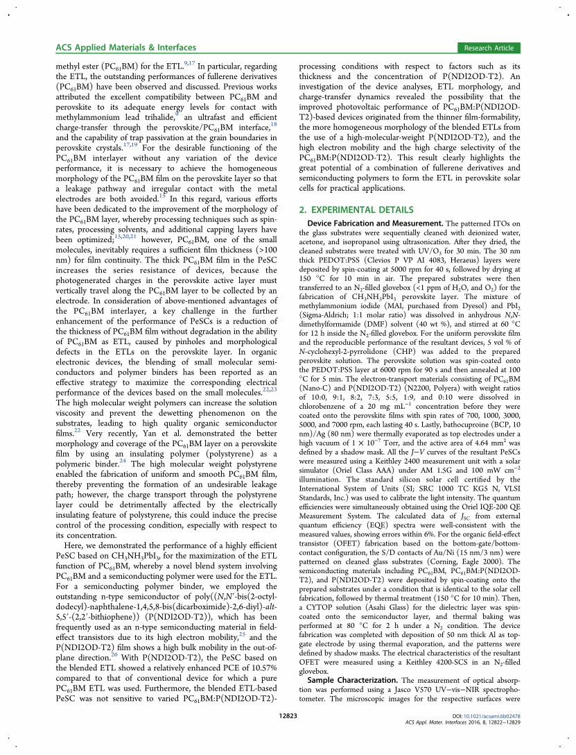
Figure 1a provides the schematic structure of the planar PeSCs,for which OSC geometry was employed, wherein the chemicalstructures of electron-transport materials including the conven-tional PC61BM and the high-molecular n-type semiconductingpolymer P(NDI2OD-T2) used in this study are shown. Afterthe formation of a PEDOT:PSS film (∼30 nm) as the HTL ona glass/ITO substrate, the compact perovskite layer (∼160 nm)
of the light harvester CH3NH3PbI3 was grown onto a preparedsubstrate by our one-step method, whereby CHP was used as asolvent additive.13 Then, for the new ETL concept, the blendedsolution of PC61BM:P(NDI2OD-T2) was simply spin-coatedon the perovskite active layer without any additional treat-ments. As shown in Figure 1b, a representative cross-sectionalimage of SEM, the respective layers in planar PeSC were clearlywell-fabricated; in particular, the thin ETL (∼40 nm) consistingof the PC61BM:P(NDI2OD-T2) blend (optimal weight ratio of9:1) covers the photoactive perovskite layer uniformly and isfree of any pinholes or morphological defects. The correspond-ing energy levels of the respective materials are depicted inFigure 1c. Considering the strong electron-withdrawing abilityof P(NDI2OD-T2) and the sufficiently low level of lowestunoccupied molecular orbital (LUMO),26 an exploration of thefeasibility of a PC61BM:P(NDI2OD-T2) blend for the ETL inplanar PeSCs is worthwhile.To investigate the potential of using PC61BM:P(NDI2OD-
T2) for the ETL in planar PeSCs, we systemically comparedthe device performances with variable weight ratios of
Figure 1. (a) Schematic device structure for the planar perovskite solar cell (PeSC) with the glass/ITO/PEDOT:PSS/CH3NH3PbI3/PC61BM:P(NDI2OD-T2)/BCP/Ag configuration and chemical structures of ETLs used in this study. (b) Cross-sectional image of resultant PeSCwith the PC61BM:P(NDI2OD-T2) ETL. (c) Corresponding energy level of each layer.
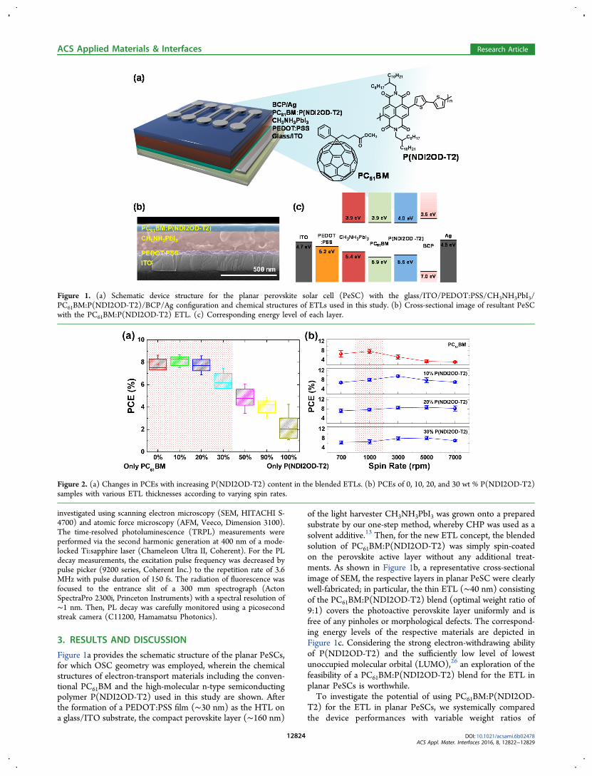
Figure 2. (a) Changes in PCEs with increasing P(NDI2OD-T2) content in the blended ETLs. (b) PCEs of 0, 10, 20, and 30 wt % P(NDI2OD-T2)samples with various ETL thicknesses according to varying spin rates.
ACS Applied Materials & Interfaces Research Article
P(NDI2OD-T2) to PC61BM and with variable ETL thicknessesby controlling spin rates. As shown in Figure 2a, the blendratios of the P(NDI2OD-T2) relative to PC61BM were firstcontrolled from 0 to 100 wt % of with a fixed ETL thickness(∼90 nm, a spin rate of 1000 rpm), because in our case the bestperformance of the pristine PC61BM ETL was achieved whenits film thickness was ∼90 nm.16 The devices employingpristine PC61BM ETLs and blended ETLs with lowconcentration of P(NDI2OD-T2) (10 and 20 wt %) exhibitedsimilar PCEs of ∼8%. Above a P(NDI2OD-T2) concentrationof 30 wt %, the device performances were gradually degraded asthe P(NDI2OD-T2) content increased, and the incorporationof 100 wt % P(NDI2OD-T2) as the ETL in planar PeSCsresulted in very poor PCE of 2.11%. Accordingly, we fixed theP(NDI2OD-T2) weight ratios of 0, 10, 20, and 30 wt %, and tofurther examine the potential of the PC61BM:P(NDI2OD-T2)ETL, we controlled its film thickness by varying the spin-coating speeds including 700 rpm (∼100 nm), 1000 rpm (∼90nm), 3000 rpm (∼40 nm), 5000 rpm (∼30 nm), and 7000 rpm(∼25 nm). As shown in Figure 2b, just beyond an optimumcondition of 1000 rpm (∼90 nm), the PeSCs with the pristinePC61BM ETL showed a rapid decrease of the PCEs with areducing ETL thickness, and the PCEs consequently droppedto the value of 3.23% under the 7000 rpm condition. This resultclearly confirms that the processing condition of pure PC61BMETL in planar PeSCs should be delicately controlled, and dueto the small molecular features of PC61BM such as a lowviscosity and dewetting from the substrates, a relatively thickfilm is required to produce high-performing devices.23 In
contrast, when the PC61BM:P(NDI2OD-T2) blends wereemployed in PeSCs as ETLs, the device performance was notsensitive to variations of the thickness conditions. All of theblended ETL-based devices exhibited PCEs of more than 6%regardless of the spin rates and P(NDI2OD-T2) content, andmore importantly, the high average PCEs of ∼8% wereachieved with the PC61BM:P(NDI2OD-T2) PeSCs, even underthe very thin condition of 7000 rpm that resulted in 25 nmthick ETLs; such results could not be obtained with the devicesusing single fullerene derivatives or an insulating polymericbinder for the morphology control of the PC61BM film.15,24
These results provide evidence that the incorporation ofP(NDI2OD-T2) into PC61BM minimizes the influence of theprocessing conditions on the device performance, which couldbe beneficial for large-area applications. More notably, higherdevice efficiencies could be achieved by modulating thethicknesses of the blended ETLs, and thereby, the PCEs ofthe optimized PeSCs using PC61BM:P(NDI2OD-T2) ETL,which were obtained in 10 wt % P(NDI2OD-T2) at 3000 rpm(∼40 nm) condition, showed a 25% increase compared withthose of the devices with the conventional PC61BM ETL.To explore the characteristics and performances of the
PC61BM:P(NDI2OD-T2) ETL in the planar PeSCs, therespectively optimized PeSCs employing pure PC61BM (∼90nm) and PC61BM:P(NDI2OD-T2) (∼40 nm) were inves-tigated, and another reference PeSC, for which a 40 nm thickpure PC61BM ETL (PC61BM_3000 rpm) with the same filmthickness as the optimized blend film was used, was alsoinvestigated for an enhanced comparative study. As shown in
Figure 3. (a) Optical absorption spectra for perovskite films with different ETLs. (b) Current−voltage characteristics and (c) external quantumefficiencies of various PeSCs. The calculated JSC from EQE spectra were 12.2, 11.1, and 14.2 mA cm−2 for PC61BM, PC61BM_3000 rpm, andPC61BM:P(NDI2OD-T2) devices, respectively. (inset) The corresponding internal quantum efficiencies. (d) Open-circuit voltage (VOC)dependence on light intensity for different PeSCs.
ACS Applied Materials & Interfaces Research Article
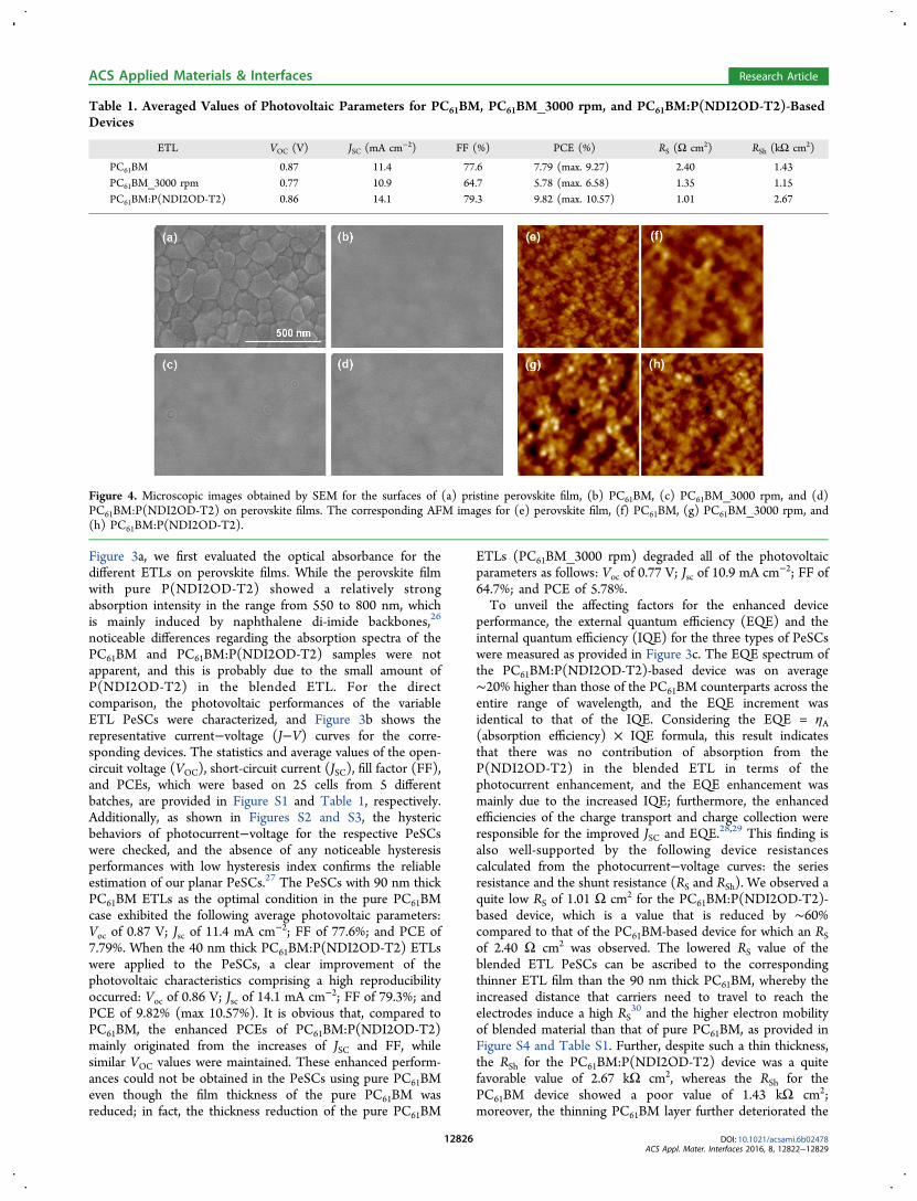
Figure 3a, we first evaluated the optical absorbance for thedifferent ETLs on perovskite films. While the perovskite filmwith pure P(NDI2OD-T2) showed a relatively strongabsorption intensity in the range from 550 to 800 nm, whichis mainly induced by naphthalene di-imide backbones,26
noticeable differences regarding the absorption spectra of thePC61BM and PC61BM:P(NDI2OD-T2) samples were notapparent, and this is probably due to the small amount ofP(NDI2OD-T2) in the blended ETL. For the directcomparison, the photovoltaic performances of the variableETL PeSCs were characterized, and Figure 3b shows therepresentative current−voltage (J−V) curves for the corre-sponding devices. The statistics and average values of the open-circuit voltage (VOC), short-circuit current (JSC), fill factor (FF),and PCEs, which were based on 25 cells from 5 differentbatches, are provided in Figure S1 and Table 1, respectively.Additionally, as shown in Figures S2 and S3, the hystericbehaviors of photocurrent−voltage for the respective PeSCswere checked, and the absence of any noticeable hysteresisperformances with low hysteresis index confirms the reliableestimation of our planar PeSCs.27 The PeSCs with 90 nm thickPC61BM ETLs as the optimal condition in the pure PC61BMcase exhibited the following average photovoltaic parameters:Voc of 0.87 V; Jsc of 11.4 mA cm−2; FF of 77.6%; and PCE of7.79%. When the 40 nm thick PC61BM:P(NDI2OD-T2) ETLswere applied to the PeSCs, a clear improvement of thephotovoltaic characteristics comprising a high reproducibilityoccurred: Voc of 0.86 V; Jsc of 14.1 mA cm−2; FF of 79.3%; andPCE of 9.82% (max 10.57%). It is obvious that, compared toPC61BM, the enhanced PCEs of PC61BM:P(NDI2OD-T2)mainly originated from the increases of JSC and FF, whilesimilar VOC values were maintained. These enhanced perform-ances could not be obtained in the PeSCs using pure PC61BMeven though the film thickness of the pure PC61BM wasreduced; in fact, the thickness reduction of the pure PC61BM
ETLs (PC61BM_3000 rpm) degraded all of the photovoltaicparameters as follows: Voc of 0.77 V; Jsc of 10.9 mA cm−2; FF of64.7%; and PCE of 5.78%.To unveil the affecting factors for the enhanced device
performance, the external quantum efficiency (EQE) and theinternal quantum efficiency (IQE) for the three types of PeSCswere measured as provided in Figure 3c. The EQE spectrum ofthe PC61BM:P(NDI2OD-T2)-based device was on average∼20% higher than those of the PC61BM counterparts across theentire range of wavelength, and the EQE increment wasidentical to that of the IQE. Considering the EQE = ηA(absorption efficiency) × IQE formula, this result indicatesthat there was no contribution of absorption from theP(NDI2OD-T2) in the blended ETL in terms of thephotocurrent enhancement, and the EQE enhancement wasmainly due to the increased IQE; furthermore, the enhancedefficiencies of the charge transport and charge collection wereresponsible for the improved JSC and EQE.28,29 This finding isalso well-supported by the following device resistancescalculated from the photocurrent−voltage curves: the seriesresistance and the shunt resistance (RS and RSh). We observed aquite low RS of 1.01 Ω cm2 for the PC61BM:P(NDI2OD-T2)-based device, which is a value that is reduced by ∼60%compared to that of the PC61BM-based device for which an RSof 2.40 Ω cm2 was observed. The lowered RS value of theblended ETL PeSCs can be ascribed to the correspondingthinner ETL film than the 90 nm thick PC61BM, whereby theincreased distance that carriers need to travel to reach theelectrodes induce a high RS
30 and the higher electron mobilityof blended material than that of pure PC61BM, as provided inFigure S4 and Table S1. Further, despite such a thin thickness,the RSh for the PC61BM:P(NDI2OD-T2) device was a quitefavorable value of 2.67 kΩ cm2, whereas the RSh for thePC61BM device showed a poor value of 1.43 kΩ cm2;moreover, the thinning PC61BM layer further deteriorated the
Table 1. Averaged Values of Photovoltaic Parameters for PC61BM, PC61BM_3000 rpm, and PC61BM:P(NDI2OD-T2)-BasedDevices
Figure 4. Microscopic images obtained by SEM for the surfaces of (a) pristine perovskite film, (b) PC61BM, (c) PC61BM_3000 rpm, and (d)PC61BM:P(NDI2OD-T2) on perovskite films. The corresponding AFM images for (e) perovskite film, (f) PC61BM, (g) PC61BM_3000 rpm, and(h) PC61BM:P(NDI2OD-T2).
ACS Applied Materials & Interfaces Research Article
shunting blocking capability of the photovoltaic device (1.15kΩ cm2 for PC61BM_3000 rpm). In addition, the degree ofrecombination regarding the PC61BM:P(NDI2OD-T2) devicewas quite weak, as confirmed by the dependence of the VOC onthe light intensity that resulted in a slope of 1.31 kT/q (Figure3d). The near-unity value of the slope (1.31 kT/q) supports thedominant bimolecular recombination with little presence oftraps in the PC61BM:P(NDI2OD-T2) device.10,31 Contrarily,the PC61BM sample showed the strong dependence of the Vocon the light intensity with a slope of 1.71 kT/q, and thisdependence was more significant in the case of thePC61BM_3000 rpm for which a slope of 2.81 kT/q wasfound. These findings indicate that the recombination ofphotogenerated charges frequently occurs through the trap sitesin the devices with PC61BM, and that a reduction of thicknessof the PC61BM ETL further activated the trap-assistedrecombination in the planar PeSCs.10 It can therefore besummarized that the blending of PC61BM with P(NDI2OD-T2) not only minimizes the resistive losses through theelectron-transport layers, but it also successfully prevents aleakage-path, and this accounts for the increased JSC and FF ofthe PC61BM:P(NDI2OD-T2) devices.To understand the relation between the morphological
characteristics of the ETLs and the corresponding PeSC-performances, and to also examine the effect of P(NDI2OD-T2) on PC61BM films, we used SEM and AFM to investigatethe morphological features of a variety of ETLs on theperovskite films. As can be seen in Figure 4a and 4e, the pristineperovskite film grown according to the CHP-additive methodshowed a uniform morphology consisting of compact grains,resulting in a moderate surface roughness of 7.090 nm. WhenPC61BM film with a sufficient thickness of 90 nm was formedon this perovskite film, the underlying perovskite layer waswell-covered by the PC61BM layer, and the film surface appearsvery smooth with a surface roughness of 1.357 nm. However,the thin film of PC61BM_3000 rpm coated on the perovskitefilm failed to uniformly cover the perovskite layer, and severalmorphological defects and the relatively rough surface of thePC61BM_3000 rpm with a surface roughness of 2.146 nm wereobserved, leading to a nonuniform contact with the metalcathode. The origin of this finding could be the inherentfeatures of the small molecular PC61BM such as a low viscosity,which limits the thickness control of the PC61BM layer, andcannot simultaneously satisfy the both the thin-thicknessformation and the uniform coverage formation for a higherdevice performance.24,32 Alternatively, in the case ofPC61BM:P(NDI2OD-T2), although the PC61BM:P(NDI2OD-T2) film is as thin as that of the PC61BM_3000 rpm, the roughsurface of the perovskite layer completely disappeared withoutany morphological defects after the coating of the PC61BM:P-(NDI2OD-T2) film, showing low surface roughness of 1.705nm. It is apparent that the blending of PC61BM with high-molecular P(NDI2OD-T2) improves the PC61BM process-ability in solution process and facilitates the formation of ahomogeneous film on the perovskite layer. This provides anintimate contact with top electrode and successfully suppressesthe leakage currents caused by direct and irregular contactsbetween the metals and the perovskite film. Taking themorphological results into account, the improved photovoltaicparameters including JSC and FF in the devices based onblended ETLs could stem from the thinner ETL thickness thanthe 90 nm thick PC61BM and the more homogeneous filmformation than that of the 40 nm thick PC61BM_3000 rpm. In
addition, as is evident in Figure S4, the higher electron mobilityand the higher charge selectivity of the PC61BM:P(NDI2OD-T2) material than those of the pure PC61BM could also supportthe better ETL performance of PC61BM:P(NDI2OD-T2)regardless of the ETL thickness.To further examine the factors for high-performing
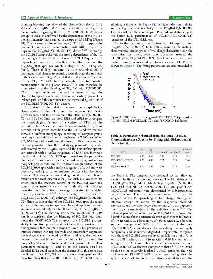
PC61BM:P(NDI2OD-T2) ETL with a focus on the materialcharacteristics, investigation of the charge dissociation and therecombination phenomena that occurred around theCH3NH3PbI3/PC61BM:P(NDI2OD-T2) interface was con-ducted using time-resolved photoluminescence (TRPL) asshown in Figure 5. The fitting parameters are also provided in
the Table 2. The samples were prepared so that they areidentical to those for working devices. The PL lifetimes forCH3NH3PbI3/PC61BM, CH3NH3PbI3/PC61BM:P(NDI2OD-T2), and CH3NH3PbI3/P(NDI2OD-T2) on glass/ITO/PEDOT:PSS substrates were determined by a biexponentialdecay function. The first decay component of τ1 can beassigned to the PL quenching of free charges through aneffective charge extraction by the respective electrodeinterlayers, and the slow decay component of τ2 can representthe charge recombination in the radiative channel.10,16 Theobtained parameters in the case of PC61BM ETL showed thedesirable values for the efficient electron quencher as follows: τ1of 1.75 ns with a 0.72 fraction, τ2 of 4.69 ns with a 0.28 fraction,and an average τ of 3.25 ns. In the case of the pureP(NDI2OD-T2), a fast decay and a slow decay that are highlycomparable and somewhat degraded, respectively, comparedwith those of PC61BM were observed, as follows: τ1 of 1.72 nswith a 0.81 fraction, τ2 of 6.36 ns with a 0.19 fraction, and anaverage τ of 3.79 ns. This inferior performance of pureP(NDI2OD-T2) as electron quencher to that of PC61BM couldbe due to the relatively localized LUMO states on the rigidbackbone of P(NDI2OD-T2), when considering that thesphere shape of fullerene derivatives can delocalize the
Figure 5. TRPL spectra of the glass/ITO/PEDOT:PSS/perovskite/PC61BM, PC61BM:P(NDI2OD-T2), and P(NDI2OD-T2) layers.
Table 2. Parameters Obtained from the Time-ResolvedPhotoluminescence Spectra by Fitting with Bi-ExponentialDecay function
LUMO state over entire surface of molecules.26,33 Interestingly,when the PC61BM:P(NDI2OD-T2) was used as the ETL, thePL lifetimes of the perovskite were further lowered with ahigher fraction of fast component than those of the purePC61BM and P(NDI2OD-T2) ETLs, as follows: τ1 of 1.59 nswith a 0.82 fraction, τ2 of 4.31 ns with a 0.18 fraction, and anaverage τ of 2.60 ns. This finding suggests that PC61BM:P-(NDI2OD-T2) guarantees the efficient extraction of thecharges generated in the perovskite layer without causing asevere recombination at the perovskite/PC61BM:P(NDI2OD-T2) interfaces, and this soundly correlates with the resultsregarding VOC dependence on the light intensity as confirmedin Figure 3d. It is therefore possible to elucidate that theimproved n-type semiconducting property of PC61BM:P-(NDI2OD-T2) facilitates a charge selectivity for electron,whereas the pristine PC61BM exhibited strong ambipolarbehavior with a low charge selectivity as confirmed by FigureS4.34 Additionally, according to previous reports, the higherelectron mobility of the electron-transport materials could bebeneficial for an efficient charge extraction due to thesuppression of the charge recombination in the solarcells.26,35 The improved charge extraction from the perovskiteto the PC61BM:P(NDI2OD-T2) ETL, as confirmed by theTRPL analyses, could therefore be highly relevant to theinherent material characteristics of PC61BM:P(NDI2OD-T2)including the higher charge selectivity and higher electronmobility. In consideration of all of these investigations, theenhanced performance of the PeSCs using PC61BM:P-(NDI2OD-T2) ETLs could originate from the followingfactors: the thinner film-formation possibility with the aid ofthe better polymer’s processing ability; a more homogeneousmorphology formation through the use of P(NDI2OD-T2)that even applies to thinner film; a more effective chargeselectivity and the higher electron mobility of the PC61BM:P-(NDI2OD-T2) material.
4. CONCLUSIONS
We successfully demonstrated the high-performing PeSCs byintroducing blended ETLs consisting of small-molecularPC61BM and polymeric P(NDI2OD-T2). The high-molecularP(NDI2OD-T2) facilitated the thinning ETL and homoge-neous coverage on the perovskite, thereby effectively reducingthe serial resistance without compromising the ETL function ofPC61BM. As a result, the PCE in the PC61BM:P(NDI2OD-T2)-based cell was considerably boosted to 10.57%, represent-ing an increase that is 25% greater than that of the conventionalPC61BM-based PeSC. Further, upon the incorporation ofP(NDI2OD-T2) into PC61BM, the variations of the PeSCperformances were not sensitive to the processing conditions ofETLs. Systematic investigations on the device analyses, ETLmorphology, and charge-transfer dynamics revealed that theenhanced performances of the PeSCs with PC61BM:P-(NDI2OD-T2) ETLs could be attributed to the thin andhomogeneous coverage of the blended ETL on perovskitelayer, as well as the electron mobility and charge selectivity ofPC61BM:P(NDI2OD-T2) for the charge-extraction process,both of which are higher than those of the pure PC61BM. Ourapproach for the incorporation of a high-molecular and highelectron-mobility polymer into a PC61BM ETL is effective andconvenient for advancing the performance and processability ofthe PeSCs in a practical terms.
■ ASSOCIATED CONTENT*S Supporting InformationThe Supporting Information is available free of charge on theACS Publications website at DOI: 10.1021/acsami.6b02478.
Statistics for photovoltaic parameters of the PeSCs,corresponding current−voltage hysteresis, and field-effectmobilities of various ETLs used in this study. (PDF)
Present Address⊥Carbon Convergence Materials Research Center, KoreaInstitute of Science and Technology (KIST), San 101,Eunha-ri, Bongdong-eup, Wanju-gun, Jeollabuk-do, 565−905Republic of Korea.
Author Contributions∥These authors contributed equally. The manuscript waswritten through contributions of all authors. All authors havegiven approval to the final version of the manuscript.
NotesThe authors declare no competing financial interest.
■ ACKNOWLEDGMENTSThis work was supported by the National Research Foundationof Korea (NRF) grant funded by the Korea government(MSIP; No. 2012M2A2A6013183).
■ REFERENCES(1) Kim, H. S.; Lee, C. R.; Im, J. H.; Lee, K. B.; Moehl, T.;Marchioro, A.; Moon, S. J.; Humphry-Baker, R.; Yum, J. H.; Moser, J.E.; Gratzel, M.; Park, N. G. Lead Iodide Perovskite Sensitized All-Solid-State Submicron Thin Film Mesoscopic Solar Cell withEfficiency Exceeding 9%. Sci. Rep. 2012, 2, 591.(2) Jeon, N. J.; Noh, J. H.; Kim, Y. C.; Yang, W. S.; Ryu, S.; Seok, S. I.Solvent Engineering for High-Performance Inorganic-Organic HybridPerovskite Solar Cells. Nat. Mater. 2014, 13, 897−903.(3) Lee, M. M.; Teuscher, J.; Miyasaka, T.; Murakami, T. N.; Snaith,H. J. Efficient Hybrid Solar Cells Based on Meso-SuperstructuredOrganometal Halide Perovskites. Science 2012, 338, 643−647.(4) Huang, J.; Shao, Y.; Dong, Q. Organometal Trihalide PerovskiteSingle Crystals: A Next Wave of Materials for 25% EfficiencyPhotovoltaics and Applications Beyond? J. Phys. Chem. Lett. 2015, 6,3218−3227.(5) Jung, H. S.; Park, N. G. Perovskite Solar Cells: from Materials toDevices. Small 2015, 11, 10−25.(6) Kojima, A.; Teshima, K.; Shirai, Y.; Miyasaka, T. OrganometalHalide Perovskites as Visible-Light Sensitizers for Photovoltaic Cells. J.Am. Chem. Soc. 2009, 131, 6050−6051.(7) Yang, W. S.; Noh, J. H.; Jeon, N. J.; Kim, Y. C.; Ryu, S.; Seo, J.;Seok, S. I. High-Performance Photovoltaic Perovskite LayersFabricated through Intramolecular Exchange. Science 2015, 348,1234−1237.(8) Snaith, H. J. Perovskites: The Emergence of a New Era for Low-Cost, High-Efficiency Solar Cells. J. Phys. Chem. Lett. 2013, 4, 3623−3630.(9) Jeng, J. Y.; Chiang, Y. F.; Lee, M. H.; Peng, S. R.; Guo, T. F.;Chen, P.; Wen, T. C. CH3NH3PbI3 Perovskite/Fullerene Planar-Heterojunction Hybrid Solar Cells. Adv. Mater. 2013, 25, 3727−3732.(10) You, J.; Hong, Z.; Yang, Y. M.; Chen, Q.; Cai, M.; Song, T. B.;Chen, C. C.; Lu, S.; Liu, Y.; Zhou, H.; Yang, Y. Low-TemperatureSolution-Processed Perovskite Solar Cells with High Efficiency andFlexibility. ACS Nano 2014, 8, 1674−1680.
ACS Applied Materials & Interfaces Research Article
(11) Vak, D.; Hwang, K.; Faulks, A.; Jung, Y.-S.; Clark, N.; Kim, D.-Y.; Wilson, G. J.; Watkins, S. E. 3D Printer Based Slot-Die Coater as aLab-to-Fab Translation Tool for Solution-Processed Solar Cells. Adv.Energy Mater. 2015, 5, 1401539.(12) Xiao, Z.; Dong, Q.; Bi, C.; Shao, Y.; Yuan, Y.; Huang, J. SolventAnnealing of Perovskite-Induced Crystal Growth for Photovoltaic-Device Efficiency Enhancement. Adv. Mater. 2014, 26, 6503−6509.(13) Jeon, Y. J.; Lee, S.; Kang, R.; Kim, J. E.; Yeo, J. S.; Lee, S. H.;Kim, S. S.; Yun, J. M.; Kim, D. Y. Planar Heterojunction PerovskiteSolar Cells with Superior Reproducibility. Sci. Rep. 2014, 4, 6953.(14) Luo, S.; Daoud, W. A. Recent Progress in Organic−InorganicHalide Perovskite Solar Cells: Mechanisms and Material Design. J.Mater. Chem. A 2015, 3, 8992−9010.(15) Seo, J.; Park, S.; Chan Kim, Y.; Jeon, N. J.; Noh, J. H.; Yoon, S.C.; Seok, S. I. Benefits of Very Thin PCBM and LiF Layers forSolution-Processed p−i−n Perovskite Solar Cells. Energy Environ. Sci.2014, 7, 2642−2646.(16) Yeo, J.-S.; Kang, R.; Lee, S.; Jeon, Y.-J.; Myoung, N.; Lee, C.-L.;Kim, D.-Y.; Yun, J.-M.; Seo, Y.-H.; Kim, S.-S.; Na, S.-I. Highly Efficientand Stable Planar Perovskite Solar Cells with Reduced GrapheneOxide Nanosheets as Electrode Interlayer. Nano Energy 2015, 12, 96−104.(17) Shao, Y.; Xiao, Z.; Bi, C.; Yuan, Y.; Huang, J. Origin andElimination of Photocurrent Hysteresis by Fullerene Passivation inCH3NH3PbI3 Planar Heterojunction Solar Cells. Nat. Commun. 2014,5, 5784.(18) Stranks, S. D.; Eperon, G. E.; Grancini, G.; Menelaou, C.;Alcocer, M. J.; Leijtens, T.; Herz, L. M.; Petrozza, A.; Snaith, H. J.Electron-Hole Diffusion Lengths Exceeding 1 Micrometer in anOrganometal Trihalide Perovskite Absorber. Science 2013, 342, 341−344.(19) Xu, J.; Buin, A.; Ip, A. H.; Li, W.; Voznyy, O.; Comin, R.; Yuan,M.; Jeon, S.; Ning, Z.; McDowell, J. J.; Kanjanaboos, P.; Sun, J. P.; Lan,X.; Quan, L. N.; Kim, D. H.; Hill, I. G.; Maksymovych, P.; Sargent, E.H. Perovskite-Fullerene Hybrid Materials Suppress Hysteresis inPlanar Diodes. Nat. Commun. 2015, 6, 7081.(20) Wang, Q.; Shao, Y.; Dong, Q.; Xiao, Z.; Yuan, Y.; Huang, J.Large Fill-Factor Bilayer Iodine Perovskite Solar Cells Fabricated by aLow-Temperature Solution-Process. Energy Environ. Sci. 2014, 7,2359−2365.(21) Li, C.; Wang, F.; Xu, J.; Yao, J.; Zhang, B.; Zhang, C.; Xiao, M.;Dai, S.; Li, Y.; Tan, Z. Efficient Perovskite/Fullerene PlanarHeterojunction Solar Cells with Enhanced Charge Extraction andSuppressed Charge Recombination. Nanoscale 2015, 7, 9771−9778.(22) Smith, J.; Zhang, W.; Sougrat, R.; Zhao, K.; Li, R.; Cha, D.;Amassian, A.; Heeney, M.; McCulloch, I.; Anthopoulos, T. D.Solution-Processed Small Molecule-Polymer Blend Organic Thin-Film Transistors with Hole Mobility Greater than 5 cm2/Vs. Adv.Mater. 2012, 24, 2441−2446.(23) Huang, Y.; Wen, W.; Mukherjee, S.; Ade, H.; Kramer, E. J.;Bazan, G. C. High-Molecular-Weight Insulating Polymers CanImprove the Performance of Molecular Solar Cells. Adv. Mater.2014, 26, 4168−4172.(24) Bai, Y.; Yu, H.; Zhu, Z.; Jiang, K.; Zhang, T.; Zhao, N.; Yang, S.;Yan, H. High Performance Inverted Structure Perovskite Solar CellsBased on a PCBM:Polystyrene Blend Electron Transport Layer. J.Mater. Chem. A 2015, 3, 9098−9102.(25) Yan, H.; Chen, Z.; Zheng, Y.; Newman, C.; Quinn, J. R.; Dotz,F.; Kastler, M.; Facchetti, A. A High-Mobility Electron-TransportingPolymer for Printed Transistors. Nature 2009, 457, 679−686.(26) Moore, J. R.; Albert-Seifried, S.; Rao, A.; Massip, S.; Watts, B.;Morgan, D. J.; Friend, R. H.; McNeill, C. R.; Sirringhaus, H. PolymerBlend Solar Cells Based on a High-Mobility Naphthalenediimide-Based Polymer Acceptor: Device Physics, Photophysics andMorphology. Adv. Energy Mater. 2011, 1, 230−240.(27) Kim, H.-S.; Park, N.-G. Parameters Affecting I-V Hysteresis ofCH3NH3PbI3 Perovskite Solar cells: Effects of Perovskite Crystal Sizeand Mesoporous TiO2 Layer. J. Phys. Chem. Lett. 2014, 5, 2927−2934.
(28) Yeo, J.-S.; Yun, J.-M.; Kim, D.-Y.; Kim, S.-S.; Na, S.-I. SuccessiveSolvent-Treated PEDOT:PSS Electrodes for Flexible ITO-FreeOrganic Photovoltaics. Sol. Energy Mater. Sol. Cells 2013, 114, 104−109.(29) Hu, M.; Bi, C.; Yuan, Y.; Xiao, Z.; Dong, Q.; Shao, Y.; Huang, J.Distinct Exciton Dissociation Behavior of Organolead TrihalidePerovskite and Excitonic Semiconductors Studied in the Same System.Small 2015, 11, 2164−2169.(30) Servaites, J. D.; Yeganeh, S.; Marks, T. J.; Ratner, M. A.Efficiency Enhancement in Organic Photovoltaic Cells: Consequencesof Optimizing Series Resistance. Adv. Funct. Mater. 2010, 20, 97−104.(31) Yeo, J.-S.; Yun, J.-M.; Kang, M.; Khim, D.; Lee, S.-H.; Kim, S.-S.;Na, S.-I.; Kim, D.-Y. An Approach for an Advanced Anode InterfacialLayer with Electron-Blocking Ability to Achieve High-EfficiencyOrganic Photovoltaics. ACS Appl. Mater. Interfaces 2014, 6, 19613−19620.(32) Hamilton, R.; Smith, J.; Ogier, S.; Heeney, M.; Anthony, J. E.;McCulloch, I.; Veres, J.; Bradley, D. D. C.; Anthopoulos, T. D. High-Performance Polymer-Small Molecule Blend Organic Transistors. Adv.Mater. 2009, 21, 1166−1171.(33) Nielsen, C. B.; Holliday, S.; Chen, H. Y.; Cryer, S. J.;McCulloch, I. Non-Fullerene Electron Acceptors for Use in OrganicSolar Cells. Acc. Chem. Res. 2015, 48, 2803−2812.(34) Qin, P.; Fang, G.; Cheng, F.; Ke, W.; Lei, H.; Wang, H.; Zhao,X. Sulfur-Doped Molybdenum Oxide Anode Interface Layer forOrganic Solar Cell Application. ACS Appl. Mater. Interfaces 2014, 6,2963−2973.(35) Di Nuzzo, D.; Aguirre, A.; Shahid, M.; Gevaerts, V. S.; Meskers,S. C.; Janssen, R. A. Improved Film Morphology Reduces ChargeCarrier Recombination into the Triplet Excited State in a SmallBandgap Polymer-Fullerene Photovoltaic Cell. Adv. Mater. 2010, 22,4321−4324.
ACS Applied Materials & Interfaces Research Article